JP5300340B2 - Process cartridge and electrophotographic apparatus - Google Patents
Process cartridge and electrophotographic apparatus Download PDFInfo
- Publication number
- JP5300340B2 JP5300340B2 JP2008161621A JP2008161621A JP5300340B2 JP 5300340 B2 JP5300340 B2 JP 5300340B2 JP 2008161621 A JP2008161621 A JP 2008161621A JP 2008161621 A JP2008161621 A JP 2008161621A JP 5300340 B2 JP5300340 B2 JP 5300340B2
- Authority
- JP
- Japan
- Prior art keywords
- charging
- resin
- photosensitive member
- electrophotographic photosensitive
- layer
- Prior art date
- Legal status (The legal status is an assumption and is not a legal conclusion. Google has not performed a legal analysis and makes no representation as to the accuracy of the status listed.)
- Expired - Fee Related
Links
Images


Abstract
Description
本発明は、プロセスカートリッジ及び電子写真装置に関する。 The present invention relates to a process cartridge and an electrophotographic apparatus.
近年、電子写真感光体に接触配置した帯電部材(接触帯電部材)に電圧を印加し、電子写真感光体を帯電する接触帯電方式を採用した電子写真装置が広く普及している。このうち、ローラー形状の接触帯電部材を電子写真感光体の表面に接触させ、これに直流電圧に交流電圧を重畳した電圧を印加することにより電子写真感光体の帯電を行う方式がAC/DC接触帯電方式である。また、接触帯電部材に直流電圧のみの電圧を印加することにより電子写真感光体の帯電を行う方式がDC接触帯電方式である。 In recent years, electrophotographic apparatuses that employ a contact charging method in which a voltage is applied to a charging member (contact charging member) disposed in contact with the electrophotographic photosensitive member to charge the electrophotographic photosensitive member have become widespread. Among them, a method of charging the electrophotographic photosensitive member by bringing a roller-shaped contact charging member into contact with the surface of the electrophotographic photosensitive member and applying a voltage obtained by superimposing an alternating voltage on a direct current voltage to this surface is an AC / DC contact. It is a charging method. Further, the DC contact charging method is a method for charging the electrophotographic photosensitive member by applying a voltage of only DC voltage to the contact charging member.
しかしながら、上述の接触帯電方式は、帯電の不均一性、直接電圧を印加することによる感光体の放電絶縁破壊の発生等が欠点として挙げられ、帯電の不均一性は特にDC接触帯電方式において顕著なものとなる。 However, the contact charging method described above has disadvantages such as non-uniform charging and the occurrence of discharge breakdown of the photoreceptor by direct application of voltage, and the non-uniform charging is particularly noticeable in the DC contact charging method. It will be something.
この帯電の不均一性は、感光体表面の各部に均一な帯電がなされず、被帯電面の移動方向に対して直角な方向にスジ状の帯電むらを生じてしまうものであり、電子写真感光体表面と帯電部材との間の過剰な摩擦時に更に顕著になる。 This non-uniformity of charging does not cause uniform charging of each part of the surface of the photoreceptor, and causes streaky charging unevenness in a direction perpendicular to the moving direction of the surface to be charged. This becomes more noticeable when excessive friction occurs between the body surface and the charging member.
例えば、プロセスカートリッジ又は電子写真装置を梱包した状態で物流を行うと、物流時の振動衝撃により、接触帯電部材が電子写真感光体に押しつけられた状態で両者が擦れ合う。 For example, when physical distribution is performed in a state where a process cartridge or an electrophotographic apparatus is packed, the contact charging member is rubbed against the electrophotographic photosensitive member due to vibration shock during distribution.
そのために、電子写真感光体表面の帯電部材との接触部分に電荷が偏在蓄積され、画像形成時に電圧を印加しても上述の電子写真感光体表面の帯電部材との摺擦部分が所望の帯電電位にならない。 For this reason, electric charges are unevenly accumulated at the contact portion of the surface of the electrophotographic photosensitive member with the charging member. There is no potential.
その結果、該摺擦部分に対応した画像領域に黒スジ又は白スジの画像不良が発生してしまう。 As a result, a black streak or white streak image defect occurs in the image area corresponding to the rubbing portion.
より具体的には、電子写真用プロセスカートリッジ又は電子写真装置に用いる電子写真感光体にはコスト等の面から有機光導電体を用いた感光体である場合が多く、また感光体表面層を形成する一般的な材料としてポリカーボネート樹脂が多く用いられる。一方、接触帯電部材にはゴム系の弾性体、特にはウレタンゴムが多く用いられている。このような場合、電子写真感光体はウレタンゴムと擦れ合うことにより正に帯電され易い。 More specifically, the electrophotographic photoreceptor used in the electrophotographic process cartridge or the electrophotographic apparatus is often a photoreceptor using an organic photoconductor from the viewpoint of cost and the like, and a photoreceptor surface layer is formed. A polycarbonate resin is often used as a general material. On the other hand, a rubber-based elastic body, particularly urethane rubber is often used for the contact charging member. In such a case, the electrophotographic photosensitive member is easily positively charged by rubbing against urethane rubber.
また、これらの有機感光体は一般的に負電荷の搬送能力を持たないために、表面が正に帯電された時、対向電荷としての負電荷が感光体中に蓄積されやすい傾向にある。その結果、上述の振動により、電子写真感光体表面層の帯電部材との接触部に正の電荷が蓄積され、振動メモリー、摺擦メモリーとなってスジ状の画像が発生する。 In addition, since these organic photoreceptors generally do not have a negative charge transport capability, when the surface is positively charged, negative charges as counter charges tend to accumulate in the photoreceptor. As a result, due to the vibration described above, positive charges are accumulated in the contact portion of the surface layer of the electrophotographic photosensitive member with the charging member, and a streak-like image is generated as a vibration memory or a rubbing memory.
上述の問題を回避するために、帯電部材から電子写真感光体を離間させる機構をプロセスカートリッジに搭載して両者の接触をなくし、振動メモリーを回避する方法がある。 In order to avoid the above-mentioned problem, there is a method of avoiding vibration memory by mounting a mechanism for separating the electrophotographic photosensitive member from the charging member on the process cartridge to eliminate contact between the two.
その他にも、特許文献1には、上述の帯電不均一性を改善するために、帯電部材と電子写真感光体との平均摩擦帯電電位の差が100V以下である帯電装置が提案されている。 In addition, Patent Document 1 proposes a charging device in which the difference in average frictional charging potential between the charging member and the electrophotographic photosensitive member is 100 V or less in order to improve the above-described charging nonuniformity.
特許文献2には、帯電部材が電子写真感光体よりも帯電系列のプラス側にあり、印加電圧0Vでの摩擦帯電による表面電位が−30V以上である接触帯電装置が提案されている。 Patent Document 2 proposes a contact charging device in which the charging member is on the plus side of the charging series with respect to the electrophotographic photosensitive member, and the surface potential due to frictional charging at an applied voltage of 0 V is −30 V or higher.
特許文献3には、電子写真感光体の10点平均粗さと接触帯電部材の10点平均粗さとの和を0.1μm以上6.0μm以下とすることで、スジ状の帯電ムラの発生を抑制する技術が提案されている。
In
特許文献4には、接触帯電部材の静摩擦係数と動摩擦係数、静摩擦係数の動摩擦係数に対する比の値及び動摩擦係数の最大値の最小値に対する比の値をそれぞれ規定することで、スジ状の帯電ムラの発生を抑制する技術が開示されている。
しかしながら、帯電部材から電子写真感光体を離間させる機構を別途設ける方法では、当該機構を設けるためのスペースがプロセスカートリッジ内に必要であり、かつ機構が複雑化するという問題点がある。 However, in the method of separately providing a mechanism for separating the electrophotographic photosensitive member from the charging member, there is a problem that a space for providing the mechanism is required in the process cartridge and the mechanism is complicated.
また、特許文献1及び特許文献2の発明では、帯電部材と電子写真感光体とに平均摩擦帯電電位の差が存する以上、振動メモリーの抑止が不十分であるという問題点がある。 Further, the inventions of Patent Document 1 and Patent Document 2 have a problem that vibration memory is not sufficiently suppressed as long as there is a difference in average frictional charging potential between the charging member and the electrophotographic photosensitive member.
本発明の目的は、上述の離間機構が無い場合でも、接触帯電方式における振動メモリー(摺擦メモリー)の問題を解決し、物流時の振動後においても欠陥を抑制し、優れた画像が得られるプロセスカートリッジ及び電子写真装置を提供することにある。 The object of the present invention is to solve the problem of vibration memory (sliding memory) in the contact charging method even without the above-described separation mechanism, and to suppress defects even after vibration during physical distribution, thereby obtaining an excellent image. To provide a process cartridge and an electrophotographic apparatus.
本発明に従って、電子写真感光体と、前記電子写真感光体に接触配置され導電性弾性層と表面層とを有する帯電部材を有し該帯電部材に負の電圧を印加して前記電子写真感光体を負に帯電させる帯電手段と、を一体に支持し、電子写真装置本体に着脱自在であるプロセスカートリッジであって、
前記帯電部材の表面層は、ポリエステルポリオール、ポリエーテルポリオール、アクリルポリオールのいずれかを、イソシアネートで硬化させたポリウレタン樹脂で構成され、
23℃湿度50%の環境下における前記電子写真感光体の表面層の帯電系列上の位置が、ポリエチレンと等しいか、ポリエチレンより正側で、かつ、ポリフェニレンオキサイドより負側か、または、ポリフェニレンオキサイドと等しく、かつ、
23℃湿度50%の環境下で圧子最大押し込み深さ1μmの条件でのユニバーサル硬度(HU)が130≦HU≦200であり、
前記電子写真感光体の表面層が、ポリ環状オレフィン樹脂と電荷輸送材とを含む
ことを特徴とするプロセスカートリッジが提供される。
また、本発明に従って、電子写真感光体と、前記電子写真感光体に接触配置され導電性弾性層と表面層とを有する帯電部材を有し該帯電部材に負の電圧を印加して前記電子写真感光体を負に帯電させる帯電手段と、を一体に支持し、電子写真装置本体に着脱自在であるプロセスカートリッジであって、
前記帯電部材の表面層は、ポリエステルポリオール、ポリエーテルポリオール、アクリルポリオールのいずれかを、イソシアネートで硬化させたポリウレタン樹脂で構成され、
前記電子写真感光体の表面層が、
23℃湿度50%の環境下で圧子最大押し込み深さ1μmの条件でのユニバーサル硬度(HU)が130≦HU≦200である層であり、かつ、
ポリ環状オレフィン樹脂と電荷輸送材とを含む
ことを特徴とするプロセスカートリッジが提供される。
According to the present invention, an electrophotographic photosensitive member, and a charging member disposed in contact with the electrophotographic photosensitive member and having a conductive elastic layer and a surface layer, and applying a negative voltage to the charging member, the electrophotographic photosensitive member is provided. A process cartridge that integrally supports the charging means for negatively charging the electrophotographic apparatus and is detachable from the main body of the electrophotographic apparatus,
The surface layer of the charging member is made of a polyurethane resin obtained by curing any of polyester polyol, polyether polyol, and acrylic polyol with isocyanate,
The position on the charged series of the surface layer of the electrophotographic photosensitive member in an environment of 23 ° C. and 50% humidity is equal to polyethylene, positive from polyethylene, negative from polyphenylene oxide, or polyphenylene oxide. Equal and
23 ° C. Ri universal hardness (HU) is 130 ≦ HU ≦ 200 der under conditions of humidity of 50% of the indenter Maximum indentation depth 1μm in an environment,
A process cartridge is provided in which the surface layer of the electrophotographic photosensitive member includes a polycyclic olefin resin and a charge transport material .
Further, according to the present invention, the electrophotographic photosensitive member, and a charging member disposed in contact with the electrophotographic photosensitive member and having a conductive elastic layer and a surface layer, and applying a negative voltage to the charging member, the electrophotographic photosensitive member is provided. A process cartridge which integrally supports a charging means for negatively charging the photosensitive member and is detachable from the electrophotographic apparatus main body,
The surface layer of the charging member is made of a polyurethane resin obtained by curing any of polyester polyol, polyether polyol, and acrylic polyol with isocyanate,
The surface layer of the electrophotographic photoreceptor is
A layer having a universal hardness (HU) of 130 ≦ HU ≦ 200 under a condition where the indenter has a maximum indentation depth of 1 μm in an environment of 23 ° C. and 50% humidity, and
Includes polycyclic olefin resin and charge transport material
A process cartridge is provided.
また、本発明に従って、上記プロセスカートリッジを具備する電子写真装置が提供される。 According to the present invention, there is also provided an electrophotographic apparatus provided with the above process cartridge.
本発明によれば、接触帯電方式における振動メモリーの問題を解決し、物流時の振動後においても欠陥を抑制し、優れた画像が得られるプロセスカートリッジ及び電子写真装置を提供することができる。 According to the present invention, it is possible to provide a process cartridge and an electrophotographic apparatus that solve the problem of vibration memory in the contact charging method, suppress defects even after vibration during distribution, and obtain an excellent image.
図1に、本発明のプロセスカートリッジを備えた電子写真装置の概略構成の一例を示す。 FIG. 1 shows an example of a schematic configuration of an electrophotographic apparatus provided with the process cartridge of the present invention.
図1において、1はドラム状の電子写真感光体であり、軸2を中心に矢印方向に所定の周速度で回転駆動される。 In FIG. 1, reference numeral 1 denotes a drum-shaped electrophotographic photosensitive member, which is driven to rotate about a shaft 2 in a direction indicated by an arrow at a predetermined peripheral speed.
回転駆動される電子写真感光体1の周面は、帯電手段3により、負の所定電位に均一に帯電され、次いで、スリット露光やレーザービーム走査露光などの露光手段(不図示)から出力される露光光(画像露光光)4を受ける。こうして電子写真感光体1の周面に、目的の画像に対応した静電潜像が順次形成されていく。帯電手段3に印加する電圧は、直流成分に交流成分を重畳した電圧、又は直流成分のみの電圧のどちらでもよい。
The peripheral surface of the electrophotographic photosensitive member 1 that is rotationally driven is uniformly charged to a predetermined negative potential by the
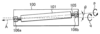
更に本発明においては、図2に示すように、電子写真感光体100の回転軸線qと、帯電手段3の一部であってローラー形状を有する帯電部材101の回転軸線pと、が所定の交差角θをもつようにして、帯電部材101を電子写真感光体100に当接されている。なお、帯電部材101の芯金105はその両端側が軸受け106a、106bによって回転自在に支持されている。その結果、帯電部材101の長手寸法を組立て誤差等の影響を最小限に抑えて設定することができるので、上記の交差角を設けていない場合に比べて、帯電部材の長手寸法を短くすることができ、かつ安定した帯電領域を保持することができる。ここで上記の交差角θは、0.1≦θ≦5°の範囲に設定される。
Further, in the present invention, as shown in FIG. 2, the rotation axis q of the electrophotographic
電子写真感光体1の周面に形成された静電潜像は、現像手段5のトナーにより現像されてトナー画像となる。次いで、電子写真感光体1の周面に形成担持されているトナー画像が、転写手段6からの転写バイアスによって順次転写されていく。転写材Pは、転写材供給手段(不図示)から電子写真感光体1と転写手段6との間(当接部)に電子写真感光体1の回転と同期して取り出されて給送される。 The electrostatic latent image formed on the peripheral surface of the electrophotographic photosensitive member 1 is developed with toner of the developing unit 5 to become a toner image. Next, the toner images formed and supported on the peripheral surface of the electrophotographic photosensitive member 1 are sequentially transferred by the transfer bias from the transfer unit 6. The transfer material P is taken out from a transfer material supply means (not shown) between the electrophotographic photoreceptor 1 and the transfer means 6 (contact portion) in synchronization with the rotation of the electrophotographic photoreceptor 1 and fed. .
トナー画像の転写を受けた転写材Pは、電子写真感光体1の周面から分離されて定着手段8へ導入されて像定着を受けることにより画像形成物(プリント、コピー)として装置外へプリントアウトされる。 The transfer material P that has received the transfer of the toner image is separated from the peripheral surface of the electrophotographic photosensitive member 1 and is introduced into the fixing means 8 to undergo image fixing, and is printed out of the apparatus as an image formed product (print, copy). Out.
トナー像転写後の電子写真感光体1の表面は、クリーニング手段7によって転写残りの現像剤(トナー)の除去を受けて清浄面化され、さらに前露光手段(不図示)からの前露光光11により除電処理された後、繰り返し画像形成に使用される。 The surface of the electrophotographic photosensitive member 1 after the transfer of the toner image is cleaned by the cleaning unit 7 after removal of the transfer residual developer (toner), and further pre-exposed light 11 from a pre-exposure unit (not shown). After being subjected to static elimination processing, the image is repeatedly used for image formation.
なお、転写手段として、例えば、ベルト状やドラム状等の中間転写体を用いた中間転写方式の転写手段を採用してもよい。 As the transfer means, for example, an intermediate transfer type transfer means using an intermediate transfer body such as a belt shape or a drum shape may be employed.
図1では、電子写真感光体1と、帯電手段3、現像手段5及びクリーニング手段7とを一体に支持してカートリッジ化して、電子写真装置本体のレール等の案内手段10を用いて電子写真装置本体に着脱自在なプロセスカートリッジ9としている。
In FIG. 1, an electrophotographic photosensitive member 1, a charging
本発明の接触式帯電部材は、電圧が印加される導電性基体である芯金、弾力性を付与する導電性弾性層、被帯電体と接触する被覆層である表面層を備える。 The contact-type charging member of the present invention includes a cored bar that is a conductive substrate to which a voltage is applied, a conductive elastic layer that imparts elasticity, and a surface layer that is a coating layer that comes into contact with a member to be charged.
本発明で使用する導電性基体である芯金は、ステンレス製の円柱である。導電性基体を構成する材料として他にも、例えば鉄、アルミニウム、チタン、銅及びニッケル等の金属やこれらの金属を含むステンレス、ジュラルミン、真鍮及び青銅等の合金が挙げられる。更にカーボンブラックや炭素繊維をプラスチックで固めた複合材料等の、剛直で導電性を示す公知の材料を使用することもできる。また、形状としては円柱形状の他に、中心部分を空洞とした円筒形状とすることも出来る。本発明では、まず上記導電性基体の外周に導電性弾性層を成形する。 The cored bar, which is a conductive substrate used in the present invention, is a stainless steel cylinder. Other examples of the material constituting the conductive substrate include metals such as iron, aluminum, titanium, copper and nickel, and alloys such as stainless steel, duralumin, brass and bronze containing these metals. Furthermore, a known material that is rigid and exhibits conductivity, such as a composite material in which carbon black or carbon fiber is solidified with plastic, can also be used. Moreover, as a shape, it can also be set as the cylindrical shape which made the center part the cavity other than a column shape. In the present invention, first, a conductive elastic layer is formed on the outer periphery of the conductive substrate.
導電性弾性層には、アルミニウム、パラジウム、鉄、銅等の金属系の粉体や繊維、ポリアセチレン、ポリピロール、ポリチオフェン等の導電性高分子粉体、カーボンブラック、酸化チタン、酸化スズ、酸化亜鉛等の金属酸化物を用いる。又は、硫化銅、硫化亜鉛等の金属化合物粉も用いることができる。又は、適当な粒子の表面を酸化スズ、酸化アンチモン、酸化インジウム、酸化モリブテン、亜鉛、アルミニウム、金、銀、銅、クロム、コバルト、鉄、鉛、白金、ロジウムを電解処理、スプレー塗工、混合振とうにより付着させた粉体でもよい。更には、アセチレンブラック、ケッチェンブラック等の導電材を分散させて導電性処理したゴムや絶縁性樹脂からなる層でもよく、又は、ゴムや絶縁性樹脂の表面を金属や他の導電性物質によってラミネート又はコートしたもの等を用いることもできる。 For conductive elastic layer, metal powder such as aluminum, palladium, iron, copper, etc., conductive polymer powder such as fiber, polyacetylene, polypyrrole, polythiophene, carbon black, titanium oxide, tin oxide, zinc oxide, etc. The metal oxide is used. Alternatively, metal compound powders such as copper sulfide and zinc sulfide can also be used. Alternatively, tin oxide, antimony oxide, indium oxide, molybdenum oxide, zinc, aluminum, gold, silver, copper, chromium, cobalt, iron, lead, platinum, rhodium are electrolyzed, spray-coated, mixed on the surface of suitable particles A powder adhered by shaking may be used. Furthermore, it may be a layer made of a conductive material such as acetylene black or ketjen black dispersed in a conductive material such as rubber or insulating resin, or the surface of the rubber or insulating resin may be made of metal or other conductive material. A laminate or a coated one can also be used.
導電性弾性層に用いられるゴムとしては、以下のものが挙げられる。例えば、EPM(エチレン・プロピレンゴム)、EPDM(エチレン・プロピレンゴム)、ノルボーネンゴム、NBR(ニトリルゴム)、クロロプレンゴム、天然ゴムである。また、イソプレンゴム、ブタジエンゴム、スチレン−ブタジエンゴム、クロロスルフォン化ポリエチレン、ヒドリンゴム、ウレタンゴム、シリコーンゴム等でもよい。絶縁性樹脂としては、ポリカーボネート、ポリエステル等が挙げられる。 Examples of the rubber used for the conductive elastic layer include the following. For example, EPM (ethylene / propylene rubber), EPDM (ethylene / propylene rubber), norbornene rubber, NBR (nitrile rubber), chloroprene rubber, and natural rubber. Further, isoprene rubber, butadiene rubber, styrene-butadiene rubber, chlorosulfonated polyethylene, hydrin rubber, urethane rubber, silicone rubber and the like may be used. Examples of the insulating resin include polycarbonate and polyester.
導電性弾性層の成形方法としては、上記の導電性弾性層の原料を混合して、例えば、押し出し成形や射出成形、圧縮成形等の公知の方法が挙げられる。また、導電性弾性層は、導電性基体の上に直接導電性弾性層を成形して作製してもよいし、チューブ形状に成形したものを導電性基体に被覆させてもよい。なお、導電性弾性層の作製後に表面を研磨して形状を整えてもよい。 Examples of the method for forming the conductive elastic layer include known methods such as extrusion molding, injection molding, and compression molding by mixing the raw materials for the conductive elastic layer. The conductive elastic layer may be produced by directly forming a conductive elastic layer on a conductive substrate, or may be formed by forming a tube shape on a conductive substrate. Note that the surface may be polished and the shape may be adjusted after the production of the conductive elastic layer.
導電性弾性層が完成した後に、その被覆層として、ポリエステルポリオール、ポリエーテルポリオール、アクリルポリオールのいずれかをイソシアネートで硬化させたポリウレタン樹脂を含有する表面層を設ける。 After the conductive elastic layer is completed, a surface layer containing a polyurethane resin obtained by curing any of polyester polyol, polyether polyol, and acrylic polyol with isocyanate is provided as the coating layer.
ポリエステルポリオールとしては、一例を挙げると、フタル酸、アジピン酸等の二塩基酸とTMP、エチレングリコール、ヘキサンジオール、ネオペンチルグリコール等のアルコール類を原料として用いたオイルフリーポリエステルポリオールが挙げられる。 Examples of polyester polyols include oil-free polyester polyols using dibasic acids such as phthalic acid and adipic acid and alcohols such as TMP, ethylene glycol, hexanediol, and neopentyl glycol as raw materials.
ポリエーテルポリオールとしては、プロピレンオキサイド、エチレンオキサイド等のアルキレンオキサイドを原料として用いたポリエーテルポリオールが挙げられる。 Examples of polyether polyols include polyether polyols using alkylene oxides such as propylene oxide and ethylene oxide as raw materials.
アクリルポリオールとしては、アクリル酸エステル、メタクリル酸エステル、ヒドロキシエチルメタクリレート(HEMA)、スチレン、アクリル酸等の共重合体であるアクリルポリオールが挙げられる。 Examples of the acrylic polyol include acrylic polyols that are copolymers of acrylic acid ester, methacrylic acid ester, hydroxyethyl methacrylate (HEMA), styrene, acrylic acid, and the like.
イソシアネート化合物としては、以下のものが挙げられる。例えば、トリレンジイソシアネート、メタキシリレンジイソシアネート、ジフェニルメタンイソシアネート、ポリメチレンポリフェニルイソシアネート等の芳香族イソシアネート化合物である。上記イソシアネートの水添加、ヘキサメチレンジイソシアネート等の脂肪族イソシアネート化合物でもよい。及びこれらのイソシアネート化合物のイソシアネート基をフェノール、ケトキシム、芳香族第2級アミン、第3級アルコール、アミド、ラクタム、複素環化合物、亜硫酸塩等でブロックしたブロックイソシアネート化合物等も挙げられる。 The following are mentioned as an isocyanate compound. For example, aromatic isocyanate compounds such as tolylene diisocyanate, metaxylylene diisocyanate, diphenylmethane isocyanate, and polymethylene polyphenyl isocyanate. Aliphatic isocyanate compounds such as water addition of the above isocyanate and hexamethylene diisocyanate may be used. And blocked isocyanate compounds in which the isocyanate groups of these isocyanate compounds are blocked with phenol, ketoxime, aromatic secondary amine, tertiary alcohol, amide, lactam, heterocyclic compound, sulfite and the like.
上記、ポリオール化合物とイソシアネート化合物は、ベンゼン、トルエン、ニトロベンゼン、ジブチルエーテル、メチルエチルケトン、ジオキサン、アセトニトリル等の溶剤で溶解できる。よって、成形の際に、下層である導電性弾性層をおかすことのない塗工法をとることが可能である。 The polyol compound and the isocyanate compound can be dissolved in a solvent such as benzene, toluene, nitrobenzene, dibutyl ether, methyl ethyl ketone, dioxane, and acetonitrile. Therefore, it is possible to adopt a coating method that does not change the lower layer of the conductive elastic layer during molding.
表面層に含有される導電材としては、酸化チタン、酸化スズ、酸化亜鉛等の金属酸化物からなる導電材、カーボンブラック、球体状炭素材料からなる導電材等があり、単独または2種類以上組み合わせて使用してもよい。 Conductive materials contained in the surface layer include conductive materials made of metal oxides such as titanium oxide, tin oxide and zinc oxide, conductive materials made of carbon black, spherical carbon materials, etc., alone or in combination of two or more. May be used.
表面層の成形方法としては、上記の表面層を構成する材料を、サンドミル、ペイントシェーカー、ダイノミル、パールミル等のビーズを利用した従来公知の分散装置を用いて公知の方法により分散させる。得られた表面層形成用の樹脂塗料を、ディッピング法やスプレーコート法により、帯電部材の表面、本発明においては導電性弾性層の上に塗工する。 As a method for forming the surface layer, the material constituting the surface layer is dispersed by a known method using a conventionally known dispersion apparatus using beads such as a sand mill, a paint shaker, a dyno mill, and a pearl mill. The obtained resin coating for forming the surface layer is applied on the surface of the charging member, in the present invention on the conductive elastic layer, by dipping or spray coating.
帯電部材の形状としてはローラー、ブラシ、ブレード、ベルト等いずれの形状をとってもよく電子写真装置の仕様、形態にあわせて選択可能である。これらの中でもローラー形状が好ましい。 The charging member may have any shape such as a roller, a brush, a blade, or a belt, and can be selected according to the specifications and form of the electrophotographic apparatus. Among these, a roller shape is preferable.
本発明における電子写真感光体は、支持体上に中間層、感光層を有する。 The electrophotographic photoreceptor in the present invention has an intermediate layer and a photosensitive layer on a support.
感光層は、本発明の構成を満足するものであれば、電荷輸送物質と電荷発生物質を同一の層に含有する単層型感光層であっても、電荷発生物質を含有する電荷発生層と電荷輸送物質を含有する電荷輸送層とに分離した積層型(機能分離型)感光層であってもよい。しかし、電子写真特性の観点からは積層型感光層が好ましい。 As long as the photosensitive layer satisfies the constitution of the present invention, even if it is a single layer type photosensitive layer containing the charge transport material and the charge generation material in the same layer, the charge generation layer containing the charge generation material and It may be a laminated (functional separation type) photosensitive layer separated into a charge transport layer containing a charge transport material. However, a laminated photosensitive layer is preferable from the viewpoint of electrophotographic characteristics.
また、積層型感光層には、支持体側から電荷発生層、電荷輸送層の順に積層した順層型感光層と、支持体側から電荷輸送層、電荷発生層の順に積層した逆層型感光層があるが、電子写真特性の観点からは順層型感光層が好ましい。 The laminated photosensitive layer has a normal layer type photosensitive layer laminated in the order of the charge generation layer and the charge transport layer from the support side, and a reverse layer type photosensitive layer laminated in the order of the charge transport layer and the charge generation layer from the support side. However, a normal photosensitive layer is preferred from the viewpoint of electrophotographic characteristics.
図3は、本発明における電子写真感光体の層構成の概略である。図3の電子写真感光体においては、支持体21上に、後述の導電層22、中間層23、電荷発生層24及び電荷輸送層25が積層されている。
FIG. 3 is an outline of the layer structure of the electrophotographic photosensitive member in the present invention. In the electrophotographic photosensitive member of FIG. 3, a
また、感光層上に、保護層を設けてもよい。その際、保護層の帯電系列上の位置は、ポリエチレンを含みポリエチレンより正側、かつポリフェニレンオキサイドを含みポリフェニレンオキサイドより負側に位置する。更に、保護層の23℃湿度50%の環境下で圧子最大押し込み深さ1μmの条件でのユニバーサル硬度(HU)が130≦HU≦200である。 Further, a protective layer may be provided on the photosensitive layer. At this time, the position of the protective layer on the charging series is located on the positive side of the polyethylene containing polyethylene and on the negative side of the polyphenylene oxide containing polyphenylene oxide. Furthermore, the universal hardness (HU) under the condition of the indenter maximum indentation depth of 1 μm in an environment of 23 ° C. and 50% humidity is 130 ≦ HU ≦ 200.
支持体としては、導電性を有していればよく(導電性支持体)、例えば、アルミニウム、アルミニウム合金、ステンレス等の金属製(合金製)の支持体を用いることができる。 As the support, it is only necessary to have conductivity (conductive support), and for example, a support made of metal (made of alloy) such as aluminum, aluminum alloy, and stainless steel can be used.
また、アルミニウム、アルミニウム合金、酸化インジウム−酸化スズ合金等を真空蒸着によって被膜形成した層を有する上記金属製支持体やプラスチック製支持体を用いることもできる。 Moreover, the said metal support body and plastic support body which have a layer in which aluminum, an aluminum alloy, an indium oxide tin oxide alloy etc. were formed into a film by vacuum deposition can also be used.
更に、カーボンブラック、酸化スズ粒子、酸化チタン粒子、銀粒子等の導電性粒子を適当な結着樹脂と共にプラスチックや紙に含浸した支持体や、導電性結着樹脂を有するプラスチック製の支持体等を用いることもできる。支持体の形状としては、円筒状、ベルト状等が挙げられるが、円筒状が好ましい。 Further, a support in which conductive particles such as carbon black, tin oxide particles, titanium oxide particles, and silver particles are impregnated into plastic or paper together with an appropriate binder resin, a plastic support having a conductive binder resin, etc. Can also be used. Examples of the shape of the support include a cylindrical shape and a belt shape, and a cylindrical shape is preferable.
また、支持体の表面は、レーザー光等の散乱による干渉縞の防止等を目的として、切削処理、粗面化処理、アルマイト処理等を施してもよい。 The surface of the support may be subjected to cutting treatment, roughening treatment, alumite treatment, etc. for the purpose of preventing interference fringes due to scattering of laser light or the like.
支持体と感光層(電荷発生層、電荷輸送層)または後述の中間層との間には、レーザー光等の散乱による干渉縞の防止や、支持体の傷の被覆を目的とした導電層を設けてもよい。 Between the support and the photosensitive layer (charge generation layer, charge transport layer) or an intermediate layer described later, there is a conductive layer for the purpose of preventing interference fringes due to scattering of laser light, etc., and covering the scratches on the support. It may be provided.
導電層は、カーボンブラック、金属粒子、金属酸化物粒子等の導電性粒子を結着樹脂に分散させて形成することができる。 The conductive layer can be formed by dispersing conductive particles such as carbon black, metal particles, and metal oxide particles in a binder resin.
導電層の膜厚は1〜40μmであることが好ましく、特に5〜35μmであることがより好ましい。 The thickness of the conductive layer is preferably 1 to 40 μm, and more preferably 5 to 35 μm.
また、支持体または導電層と感光層(電荷発生層、電荷輸送層)との間には、バリア機能や接着機能を有する中間層を設ける。中間層は、感光層の接着性改良、塗工性改良、支持体からの電荷注入性改良、感光層の電気的破壊に対する保護等のために形成される。 Further, an intermediate layer having a barrier function or an adhesion function is provided between the support or the conductive layer and the photosensitive layer (charge generation layer, charge transport layer). The intermediate layer is formed for the purpose of improving the adhesion of the photosensitive layer, improving the coating property, improving the charge injection from the support, protecting the photosensitive layer from electrical breakdown, and the like.
中間層は、アクリル樹脂、アリル樹脂、アルキッド樹脂、エチルセルロース樹脂、エチレン−アクリル酸コポリマー、エポキシ樹脂、カゼイン樹脂、シリコーン樹脂、ゼラチン樹脂、フェノール樹脂等の材料を用いて形成することができる。又は、ブチラール樹脂、ポリアクリレート樹脂、ポリアセタール樹脂、ポリアミドイミド樹脂、ポリアミド樹脂、ポリアリルエーテル樹脂、ポリイミド樹脂、ポリウレタン樹脂でもよい。更には、ポリエステル樹脂、ポリエチレン樹脂、ポリカーボネート樹脂、ポリスチレン樹脂、ポリスルホン樹脂、ポリビニルアルコール樹脂、ポリブタジエン樹脂、ポリプロピレン樹脂、ユリア樹脂等の樹脂や、酸化アルミニウム等の材料を用いてもよい。 The intermediate layer can be formed using a material such as an acrylic resin, an allyl resin, an alkyd resin, an ethylcellulose resin, an ethylene-acrylic acid copolymer, an epoxy resin, a casein resin, a silicone resin, a gelatin resin, or a phenol resin. Alternatively, a butyral resin, polyacrylate resin, polyacetal resin, polyamideimide resin, polyamide resin, polyallyl ether resin, polyimide resin, or polyurethane resin may be used. Furthermore, a resin such as a polyester resin, a polyethylene resin, a polycarbonate resin, a polystyrene resin, a polysulfone resin, a polyvinyl alcohol resin, a polybutadiene resin, a polypropylene resin, or a urea resin, or a material such as aluminum oxide may be used.
中間層の膜厚は0.05〜10μmであることが好ましく、特には0.3〜5μmであることがより好ましい。 The film thickness of the intermediate layer is preferably 0.05 to 10 μm, and more preferably 0.3 to 5 μm.
本発明の電子写真感光体に用いられる電荷発生物質としては、例えば、モノアゾ、ジスアゾ、トリスアゾ等のアゾ顔料や、金属フタロシアニン、非金属フタロシアニン等のフタロシアニン顔料や、インジゴ、チオインジゴ等のインジゴ顔料が挙げられる。又は、ペリレン酸無水物、ペリレン酸イミド等のペリレン顔料でもよい。アンスラキノン、ピレンキノン、ジベンズピレンキノン等の多環キノン顔料も用いることができる。又は、スクワリリウム色素や、ピリリウム塩及びチアピリリウム塩や、トリフェニルメタン色素でもよい。セレン、セレン−テルル、アモルファスシリコン等の無機物質、でもよい。更には、キナクリドン顔料、アズレニウム塩顔料、キノシアニン等のシアニン染料、アントアントロン顔料、ピラントロン顔料、キサンテン色素、キノンイミン色素、スチリル色素、硫化カドミウム、酸化亜鉛等も挙げられる。これら電荷発生物質は1種のみ用いてもよく、2種以上用いてもよい。 Examples of the charge generating material used in the electrophotographic photoreceptor of the present invention include azo pigments such as monoazo, disazo, and trisazo, phthalocyanine pigments such as metal phthalocyanine and nonmetal phthalocyanine, and indigo pigments such as indigo and thioindigo. It is done. Alternatively, perylene pigments such as perylene acid anhydride and perylene imide may be used. Polycyclic quinone pigments such as anthraquinone, pyrenequinone and dibenzpyrenequinone can also be used. Alternatively, squarylium dyes, pyrylium salts and thiapyrylium salts, and triphenylmethane dyes may be used. It may be an inorganic substance such as selenium, selenium-tellurium or amorphous silicon. Further examples include cyanine dyes such as quinacridone pigments, azulenium salt pigments, quinocyanine, anthanthrone pigments, pyranthrone pigments, xanthene dyes, quinoneimine dyes, styryl dyes, cadmium sulfide, and zinc oxide. These charge generation materials may be used alone or in combination of two or more.
電荷発生層に用いられる結着樹脂としては、例えば、アクリル樹脂、アリル樹脂、アルキッド樹脂、エポキシ樹脂、ジアリルフタレート樹脂、シリコーン樹脂、スチレン−ブタジエンコポリマー、フェノール樹脂が挙げられる。ブチラール樹脂、ベンザール樹脂、ポリアクリレート樹脂、ポリアセタール樹脂、ポリアミドイミド樹脂、ポリアミド樹脂、ポリアリルエーテル樹脂、ポリアリレート樹脂、ポリイミド樹脂でもよい。ポリウレタン樹脂、ポリエステル樹脂、ポリエチレン樹脂、ポリカーボネート樹脂、ポリスチレン樹脂、ポリスルホン樹脂、ポリビニルアセタール樹脂、ポリブタジエン樹脂、ポリプロピレン樹脂でもよい。又は、メタクリル樹脂、ユリア樹脂、塩化ビニル−酢酸ビニルコポリマー、酢酸ビニル樹脂、塩化ビニル樹脂等も挙げられる。特には、ブチラール樹脂等が好ましい。これらは単独、混合または共重合体として1種または2種以上用いることができる。 Examples of the binder resin used for the charge generation layer include acrylic resin, allyl resin, alkyd resin, epoxy resin, diallyl phthalate resin, silicone resin, styrene-butadiene copolymer, and phenol resin. Butyral resin, benzal resin, polyacrylate resin, polyacetal resin, polyamideimide resin, polyamide resin, polyallyl ether resin, polyarylate resin, polyimide resin may be used. Polyurethane resin, polyester resin, polyethylene resin, polycarbonate resin, polystyrene resin, polysulfone resin, polyvinyl acetal resin, polybutadiene resin, polypropylene resin may be used. Alternatively, a methacrylic resin, a urea resin, a vinyl chloride-vinyl acetate copolymer, a vinyl acetate resin, a vinyl chloride resin, and the like can be given. In particular, a butyral resin or the like is preferable. These can be used singly or in combination of two or more as a mixture or copolymer.
電荷発生層は、電荷発生物質を結着樹脂及び溶剤と共に分散して得られる電荷発生層用塗布液を塗布し、これを乾燥させることによって形成することができる。分散方法としては、ホモジナイザー、超音波分散機、ボールミル、サンドミル、ロールミル、振動ミル、アトライター、液衝突型高速分散機等を用いた方法が挙げられる。電荷発生物質と結着樹脂との割合は、1:0.3〜1:4(質量比)の範囲が好ましい。 The charge generation layer can be formed by applying a charge generation layer coating solution obtained by dispersing a charge generation material together with a binder resin and a solvent and drying the coating solution. Examples of the dispersion method include a method using a homogenizer, an ultrasonic disperser, a ball mill, a sand mill, a roll mill, a vibration mill, an attritor, a liquid collision type high-speed disperser, and the like. The ratio between the charge generating material and the binder resin is preferably in the range of 1: 0.3 to 1: 4 (mass ratio).
電荷発生層用塗布液に用いられる溶剤は、使用する結着樹脂や電荷発生物質の溶解性や分散安定性から選択されるが、有機溶剤としてはアルコール、スルホキシド、ケトン、エーテル、エステル、脂肪族ハロゲン化炭化水素、芳香族化合物等が挙げられる。 The solvent used in the coating solution for the charge generation layer is selected from the solubility and dispersion stability of the binder resin and charge generation material to be used. As the organic solvent, alcohol, sulfoxide, ketone, ether, ester, aliphatic Examples thereof include halogenated hydrocarbons and aromatic compounds.
電荷発生層の膜厚は5μm以下であることが好ましく、特には0.1〜2μmであることがより好ましい。 The thickness of the charge generation layer is preferably 5 μm or less, and more preferably 0.1 to 2 μm.
また、電荷発生層には、種々の増感剤、酸化防止剤、紫外線吸収剤、可塑剤等を必要に応じて添加することもできる。 In addition, various sensitizers, antioxidants, ultraviolet absorbers, plasticizers, and the like can be added to the charge generation layer as necessary.
電荷輸送材料は正孔輸送材料であって、これを1種のみ用いてもよく、2種以上用いてもよい。電荷輸送材料としては、トリアリールアミン系化合物、ヒドラゾン化合物、スチルベン化合物、ピラゾリン系化合物、オキサゾール系化合物、トリアリルメタン系化合物及びチアゾール系化合物等が挙げられる。 The charge transport material is a hole transport material and may be used alone or in combination of two or more. Examples of the charge transport material include triarylamine compounds, hydrazone compounds, stilbene compounds, pyrazoline compounds, oxazole compounds, triallylmethane compounds, and thiazole compounds.
電荷輸送材料は、炭素数6以上10以下のアルキル基を有するヒドラゾン化合物、炭素数6以上10以下のアルキル基を有するトリアリールアミン化合物が好ましい。
電荷輸送材料としては、下記構造式(3)で示される炭素数6以上10以下のアルキル基を有するヒドラゾン化合物、下記構造式(4)で示される炭素数6以上10以下のアルキル基を有するトリアリールアミン化合物が挙げられる。

(R 1 〜R 10 のうち少なくとも一つは炭素数6〜10のアルキル基である。炭素数6〜10のアルキル基でないものは、それぞれ同一又は異なって、水素原子、置換基を有してもよいアルキル基、又は置換基を有してもよいアルコキシ基である。また、それぞれが互いに結合して芳香環を成していてもよい。R 11 は置換基を有してもよい芳香族基であり、有してよい置換基は、メチル基、エチル基、ハロゲン基、無置換またはメチル基を有するジアルキルアミノ基(アルキル基の炭素数は2以下)、ベンジルアルキルアミノ基(アルキル基の炭素数は2以下)、ジベンジルアミノ基、アルキルアリールアミノ基(アルキル基の炭素数は2以下)、ジアリールアミノ基である。)
(上記式(4)中、R 101 〜R 128 は水素原子、置換基を有してもよいアルキル基を示す。さらに、R 101 〜R 120 の少なくとも2つは、炭素数6〜10のアルキル基である。ただし、同一ベンゼン環上には、2つ以上の炭素数6〜10のアルキル基を有さない。Xは下記群より選ばれる構造を有する。)
The charge transport material is preferably a hydrazone compound having an alkyl group having 6 to 10 carbon atoms and a triarylamine compound having an alkyl group having 6 to 10 carbon atoms.
Examples of the charge transport material include a hydrazone compound having an alkyl group having 6 to 10 carbon atoms represented by the following structural formula (3), and a tria having an alkyl group having 6 to 10 carbon atoms represented by the following structural formula (4). Examples include a reelamine compound.
(At least one of R 1 to R 10 is an alkyl group having 6 to 10 carbon atoms. Those that are not alkyl groups having 6 to 10 carbon atoms are the same or different and each has a hydrogen atom or a substituent. R 11 is an aromatic group which may have a substituent , each of which may be bonded to each other to form an aromatic ring. The substituents that may be included are methyl, ethyl, halogen, unsubstituted or dialkylamino groups having a methyl group (the alkyl group has 2 or less carbon atoms), benzylalkylamino groups (of the alkyl group And a dibenzylamino group, an alkylarylamino group (the carbon number of the alkyl group is 2 or less), and a diarylamino group.)
(Shown in the
その理由であるが、炭素数6以上10以下のアルキル基を有するため、分子同士が集まりにくい。さらに、樹脂バインダーを含有する電荷輸送層中でも、樹脂種に関係なく均一に存在することができるため、電荷輸送材料のミクロドメイン(電荷のトラップサイト)を形成しにくくなる。その結果、電子写真感光体と帯電部材との摺擦によって発生した、電子写真感光体内の電荷の蓄積が抑制され、スジ画像といった画像不良も抑制されると考えられる。 The reason is that since the alkyl group has 6 to 10 carbon atoms, molecules are unlikely to gather. Further, even in the charge transport layer containing a resin binder, it can be present uniformly regardless of the resin type, and therefore it is difficult to form micro domains (charge trap sites) of the charge transport material. As a result, it is considered that accumulation of electric charges in the electrophotographic photosensitive member caused by rubbing between the electrophotographic photosensitive member and the charging member is suppressed, and image defects such as streak images are also suppressed.
炭素数6以上10以下のアルキル基を有するヒドラゾン化合物の具体例を表1に、炭素数6以上10以下のアルキル基を有するトリアリールアミン化合物の具体例を表2に示すが、それらに限定されるものではない。 Specific examples of hydrazone compounds having an alkyl group having 6 to 10 carbon atoms are shown in Table 1, and specific examples of triarylamine compounds having an alkyl group having 6 to 10 carbon atoms are shown in Table 2, but are not limited thereto. It is not something.
なお、表1のヒドラゾン化合物は、芳香族基を有する。この芳香族基には炭素数6〜10のアルキル基、置換基を有してもよいアルキル基、又は置換基を有してもよいアルコキシ基を置換基として有してよい。また、芳香族基のうち少なくとも一つは、メチル基、エチル基、ハロゲン基、無置換またはメチル基を有するジアルキルアミノ基(アルキル基の炭素数は2以下)を置換基として有してもよい。更には、ベンジルアルキルアミノ基(アルキル基の炭素数は2以下)、ジベンジルアミノ基、アルキルアリールアミノ基(アルキル基の炭素数は2以下)、ジアリールアミノ基を置換基として有してもよい。 In addition, the hydrazone compound of Table 1 has an aromatic group. This aromatic group may have, as a substituent, an alkyl group having 6 to 10 carbon atoms, an alkyl group that may have a substituent, or an alkoxy group that may have a substituent. Further, at least one of the aromatic groups may have a methyl group, an ethyl group, a halogen group, an unsubstituted or dialkylamino group having a methyl group (the alkyl group has 2 or less carbon atoms) as a substituent. . Furthermore, it may have a benzylalkylamino group (the carbon number of the alkyl group is 2 or less), a dibenzylamino group, an alkylarylamino group (the carbon number of the alkyl group is 2 or less), or a diarylamino group as a substituent. .
表2のトリアリールアミン化合物は、置換基を有してもよいアルキル基、又は炭素数6〜10のアルキル基を置換基として有してもよい。ただし、同一ベンゼン環上には、2つ以上の炭素数6〜10のアルキル基を有さないものとする。 The triarylamine compound of Table 2 may have an alkyl group which may have a substituent or an alkyl group having 6 to 10 carbon atoms as a substituent. However, two or more alkyl groups having 6 to 10 carbon atoms are not included on the same benzene ring.
本発明の電荷輸送層に用いる結着樹脂としては、例えば、ポリエチレン樹脂やポリプロピレン樹脂等のポリオレフィン樹脂、ポリフェニレンオキサイド樹脂、ポリ環状オレフィン樹脂から構成される。 The binder resin used in the charge transport layer of the present invention is composed of, for example, a polyolefin resin such as a polyethylene resin or a polypropylene resin, a polyphenylene oxide resin, or a polycyclic olefin resin.
ポリ環状オレフィン樹脂とは、環状オレフィンを重合させて得られる重合体をいい、環状オレフィンのみを重合させて得られる重合体であっても、環状オレフィンとそれ以外のモノマーとを共重合させて得られる重合体であってもよい。また、環状オレフィンとは、1つ以上のC=C(炭素間の二重結合)を持つ環式炭化水素化合物をいう。 The polycyclic olefin resin refers to a polymer obtained by polymerizing a cyclic olefin, and even a polymer obtained by polymerizing only a cyclic olefin is obtained by copolymerizing a cyclic olefin and other monomers. It may be a polymer. Moreover, a cyclic olefin means the cyclic hydrocarbon compound which has 1 or more C = C (double bond between carbon).
また、ポリ環状オレフィン樹脂としては、例えば、エチレンとジシクロペンタジエン類との共重合体、エチレンとノルボルネン系化合物との共重合体が挙げられる。又は、シクロペンタジエン誘導体の開環重合体、シクロへキサジエン誘導体の開環重合体、シクロペンタジエン誘導体の開環共重合体、シクロへキサジエン誘導体の開環共重合体及びそれらの水素添加物等でもよい。 Examples of the polycyclic olefin resin include a copolymer of ethylene and dicyclopentadiene, and a copolymer of ethylene and a norbornene compound. Alternatively, a ring-opening polymer of a cyclopentadiene derivative, a ring-opening polymer of a cyclohexadiene derivative, a ring-opening copolymer of a cyclopentadiene derivative, a ring-opening copolymer of a cyclohexadiene derivative, and hydrogenated products thereof may be used. .
以下に、ポリ環状オレフィン樹脂が有する繰り返し構造単位の具体例を挙げる。 Below, the specific example of the repeating structural unit which polycyclic olefin resin has is given.
また、本発明で用いられるポリ環状オレフィン樹脂としては、ガラス転移温度(Tg)が100℃以上170℃以下のものが好ましい。なお、ポリ環状オレフィン樹脂が共重合体の場合、共重合比を変えることで、そのガラス転移温度(Tg)を制御することができる。 The polycyclic olefin resin used in the present invention preferably has a glass transition temperature (Tg) of 100 ° C. or higher and 170 ° C. or lower. When the polycyclic olefin resin is a copolymer, the glass transition temperature (Tg) can be controlled by changing the copolymerization ratio.
本発明において、ポリ環状オレフィン樹脂のガラス転移温度は、セイコー電子工業(株)製の熱分析装置(商品名:SSC5200H)を用いて測定した。具体的には、23℃から280℃まで5℃/minの昇温速度で測定し、得られたチャートの固体側の接線と転移温度域の急峻な位置の接線との交点をガラス転移温度とした。 In the present invention, the glass transition temperature of the polycyclic olefin resin was measured using a thermal analyzer (trade name: SSC5200H) manufactured by Seiko Denshi Kogyo Co., Ltd. Specifically, the temperature was measured from 23 ° C. to 280 ° C. at a rate of temperature increase of 5 ° C./min, and the intersection of the solid side tangent of the obtained chart and the tangent at the sharp position of the transition temperature range was defined as the glass transition temperature. did.
本発明においては、ポリ環状オレフィン樹脂の中でも、下記一般式(1)で示される繰り返し構造単位及び下記構造式(2)で示される繰り返し構造単位を有する共重合体が特に好ましい。 In the present invention, among polycyclic olefin resins, a copolymer having a repeating structural unit represented by the following general formula (1) and a repeating structural unit represented by the following structural formula (2) is particularly preferable.
ポリ環状オレフィン樹脂の市販されているものとしては、三井化学(株)製の「アペル(登録商標)」や、チコナ社製の「トパス(登録商標)」等が挙げられる。 Examples of commercially available polycyclic olefin resins include “Apel (registered trademark)” manufactured by Mitsui Chemicals, Inc., “Topas (registered trademark)” manufactured by Chicona Corporation, and the like.
電荷輸送層の膜厚は5〜40μmであることが好ましく、特には10〜35μmであることがより好ましい。 The thickness of the charge transport layer is preferably 5 to 40 μm, and more preferably 10 to 35 μm.
また、電荷輸送層には、酸化防止剤、紫外線吸収剤、可塑剤等を必要に応じて添加することもできる。また、フッ素原子含有樹脂やシリコーン含有樹脂等を含有させても良い。また前記樹脂により構成される微粒子を含有してもよい。また、金属酸化物微粒子や無機微粒子を含有してもよい。ただし、電荷輸送層を電子写真感光体の表面層として用いる場合は、その帯電列の位置に影響を及ぼさない範囲でそれらを含有させることができる。 In addition, an antioxidant, an ultraviolet absorber, a plasticizer, and the like can be added to the charge transport layer as necessary. Further, a fluorine atom-containing resin or a silicone-containing resin may be contained. Moreover, you may contain the microparticles | fine-particles comprised with the said resin. Further, metal oxide fine particles and inorganic fine particles may be contained. However, when the charge transport layer is used as the surface layer of the electrophotographic photosensitive member, it can be contained in a range that does not affect the position of the charged column.
上記各層の塗布液を塗布する際には、例えば、浸漬塗布法(浸漬コーティング法)、スプレーコーティング法、スピンナーコーティング法、ローラーコーティング法、マイヤーバーコーティング法、ブレードコーティング法等の塗布方法を用いることができる。 When applying the coating liquid for each of the above layers, for example, a coating method such as a dip coating method (dip coating method), a spray coating method, a spinner coating method, a roller coating method, a Meyer bar coating method, a blade coating method, or the like should be used. Can do.
本発明においては、帯電列の測定は以下のように行なう。まず、電子写真感光体の表面層と同じ組成、同じ厚みの膜をガラス板上に形成する。測定環境23℃50%RHのもとで、測定したい塗膜面が上になるようにガラス板を平らな場所に置き、一時的に接地して塗膜上の電荷を0にする。次に、各々20μm程度の、ポリエチレン樹脂のみで形成した膜、並びにポリフェニレンオキサイド樹脂単独で形成した膜を用意し、先のガラス板上塗膜に10回程度往復させて擦りつけ、引き離す。その後速やかに、ガラス板上の電荷を静電気測定装置により測定する。同一条件での測定回数は10回とする。 In the present invention, the charged column is measured as follows. First, a film having the same composition and the same thickness as the surface layer of the electrophotographic photosensitive member is formed on a glass plate. Under a measurement environment of 23 ° C. and 50% RH, the glass plate is placed on a flat place so that the coating surface to be measured is on top, and temporarily grounded to zero the charge on the coating film. Next, a film made of only a polyethylene resin having a thickness of about 20 μm and a film formed of a polyphenylene oxide resin alone are prepared, rubbed back and forth about 10 times on the coating film on the glass plate, and pulled apart. Immediately thereafter, the electric charge on the glass plate is measured by a static electricity measuring device. The number of measurements under the same conditions is 10 times.
以上の操作を行い、電子写真感光体表面層と、ポリエチレン、並びにポリフェニレンオキサイドとの帯電系列の関係を決定する。なお、同一組み合わせの回の測定中、5回以上極性の逆転が起こった場合は、それらの帯電系列上の位置は等しいものと判断する。 The above operation is performed to determine the relationship of the charge series of the electrophotographic photoreceptor surface layer, polyethylene, and polyphenylene oxide. In addition, when the polarity reversal occurs five times or more during the measurement of the same combination, the positions on the charging series are determined to be equal.
ユニバーサル硬度(HU)は、圧子に連続的に荷重をかけ、荷重下での押し込み深さを直読することにより連続的硬さが求められる微小硬さ測定装置フィシャースコープH100V(フィッシャーインスツルメンツ社製)を用いて測定することができる。圧子としては対面角136°のビッカース四角錐ダイヤモンド圧子を使用する。更に具体的には、圧子押し込み深さを1μmに設定し、押し込み深さが1μmに達するまで段階的に荷重をかけ、測定する。電子写真感光体のユニバーサル硬度(HU)は、定めた最終押し込み深さに圧子が到達したときの荷重の値から求めることができる。 Universal hardness (HU) is a microhardness measuring device, Fischerscope H100V (manufactured by Fischer Instruments Inc.), which requires continuous hardness by applying a continuous load to the indenter and directly reading the indentation depth under the load. Can be measured. As the indenter, a Vickers square pyramid diamond indenter having a facing angle of 136 ° is used. More specifically, the indenter indentation depth is set to 1 μm, and a load is applied stepwise until the indentation depth reaches 1 μm. The universal hardness (HU) of the electrophotographic photosensitive member can be determined from the value of the load when the indenter reaches a predetermined final indentation depth.
電子写真感光体表面層の帯電系列上の位置がポリエチレンを含みポリエチレンより正側かつポリフェニレンオキサイドを含みポリフェニレンオキサイドより負側に位置しているとする。この状態で表面層の23℃湿度50%の環境下で圧子最大押し込み深さ1μmの条件でのユニバーサル硬度(HU)が130≦HU≦200であるとき、カートリッジ振動時の振動メモリー、摺擦メモリーが抑制される理由はまだ明確ではない。だが、以下の理由であると推測される。 It is assumed that the position of the electrophotographic photosensitive member surface layer on the charging series includes polyethylene and is located on the positive side of polyethylene and polyphenylene oxide on the negative side of polyphenylene oxide. In this state, when the universal hardness (HU) is 130 ≦ HU ≦ 200 under the condition that the indenter has a maximum indentation depth of 1 μm in an environment where the surface layer has a temperature of 23 ° C. and a humidity of 50%, vibration memory and rubbing memory during cartridge vibration The reason for the suppression is not yet clear. However, it is presumed that the reason is as follows.
帯電部材表面層が、ポリエステルポリオール、ポリエーテルポリオール、アクリルポリオールのいずれかをイソシアネートで硬化させたポリウレタン樹脂で構成された帯電部材を使用した場合を考える。そして、電子写真感光体の表面層を構成する樹脂として例えばポリカーボネートを使用した場合を考える。ポリカーボネートの帯電系列位置は、帯電部材表面層の上述ウレタン樹脂の帯電系列位置の近傍には存在せず、離れたプラスの位置に存在する。 Consider a case where the charging member surface layer uses a charging member made of a polyurethane resin obtained by curing any of polyester polyol, polyether polyol, and acrylic polyol with isocyanate. Consider a case where, for example, polycarbonate is used as the resin constituting the surface layer of the electrophotographic photosensitive member. The charged series position of the polycarbonate does not exist in the vicinity of the charged series position of the urethane resin on the surface layer of the charging member, but exists at a positive position apart from the above.
また、帯電部材と電子写真感光体各表面層の帯電系列は、各々を構成する樹脂に大きく左右されることから、両者の摺擦時、電子写真感光体がプラスに帯電し、かつ電子写真感光体にプラスのメモリーが形成されやすい。負帯電型の電子写真感光体においては、感光層はマイナス電荷の搬送性をほとんど持たないため、プラスの極性のメモリーは消失しにくく、長期にわたり画像欠陥として発生するのである。 In addition, since the charging series of each surface layer of the charging member and the electrophotographic photosensitive member is greatly influenced by the resin constituting each, the electrophotographic photosensitive member is positively charged when the two are rubbed, and the electrophotographic photosensitive member is charged. A positive memory is easily formed on the body. In a negatively charged electrophotographic photosensitive member, the photosensitive layer has almost no negative charge transportability, so that the memory with a positive polarity is not easily lost, and it is generated as an image defect over a long period of time.
電子写真感光体の表面層の帯電系列上の位置が、ポリエチレンを含みポリエチレンより正側、かつポリフェニレンオキサイドを含みポリフェニレンオキサイドより負側に位置していれば、帯電系列上の位置が帯電部材の表面層と近い。又は、電子写真感光体表面層がわずかに負側に位置している。よって、物流時の振動衝撃による摩擦帯電量が小さくなる。又は、すぐさま消失する程度のマイナスに電子写真感光体が帯電するだけであるので、振動メモリーが抑制されスジ状の画像も抑制されるのである。 If the position of the surface layer of the electrophotographic photosensitive member on the charging series includes polyethylene and is located on the positive side of the polyethylene and on the negative side of the polyphenylene oxide and contains polyphenylene oxide, the position on the charging series is the surface of the charging member. Close to the layer. Alternatively, the electrophotographic photosensitive member surface layer is slightly on the negative side. Therefore, the triboelectric charge amount due to the vibration shock during distribution is reduced. Alternatively, since the electrophotographic photosensitive member is only charged to the minus of the extent that it disappears immediately, the vibration memory is suppressed and the streak-like image is also suppressed.
更に、23℃湿度50%の環境下で圧子最大押し込み深さ1μmの条件でのユニバーサル硬度(HU)が130≦HU≦200である場合、電子写真感光体を電子写真装置に搭載した場合の耐久削れ量が好適で、上述の振動メモリーもすぐ消失すると考えられる。 Further, when the universal hardness (HU) under the condition that the indenter has a maximum indentation depth of 1 μm in an environment of 23 ° C. and 50% humidity is 130 ≦ HU ≦ 200, the durability when the electrophotographic photosensitive member is mounted on the electrophotographic apparatus. It is considered that the amount of shaving is suitable, and the above-mentioned vibration memory will also disappear soon.
具体的には、HU<130である場合、これとは別に、感光体表面層としての強度が不足し、上述の振動時に感光体表面にキズがつきやすくなり、不良画像となってしまう。HU>200である場合、画像耐久削れ量が減少するものの、振動・摺擦によって一旦感光体内部に蓄積したメモリーが消失しにくく、スジ画像も長期にわたって発生してしまうと推測される。 Specifically, when HU <130, the strength of the surface layer of the photoconductor is insufficient, and the surface of the photoconductor is easily scratched during the vibration described above, resulting in a defective image. When HU> 200, although the amount of image durability wear is reduced, it is presumed that the memory once accumulated in the photoreceptor due to vibration and rubbing is not easily lost, and streak images are also generated over a long period of time.
先述のとおり、本発明においては、図2に示すように、電子写真感光体100の回転軸線qとローラー形状帯電部材101の回転軸線pとが0.1≦θ≦5°の交差角θをもっている。このように交差角を持つ場合、両者の摺擦における振動メモリーはより厳しくなるものと推測できるが、本発明においては、このような場合でも振動メモリーに伴なう画像スジを抑制することができる。
As described above, in the present invention, as shown in FIG. 2, the rotation axis q of the electrophotographic
以下、具体的な実施例を挙げて、本発明をより詳細に説明する。なお、実施例中の「部」は質量部を意味する。 Hereinafter, the present invention will be described in more detail with reference to specific examples. In the examples, “part” means part by mass.
<合成例1>
(本発明の正孔輸送材料の合成例1)
4-Hexylaniline(東京化成工業株式会社製)8.9質量部と1-Bromo-4-hexylbenzene (東京化成工業株式会社製)12.0質量部とTHF300質量部とを、窒素フローした三口フラスコ中に入れる。t-BuONa10%水溶液50質量部を滴下後、(1,1'-Bis(diphenylphosphino)ferrocene)dichloropalladium(II)(アルドリッチ社製)1質量部を加えて5時間還流した。
<Synthesis Example 1>
(Synthesis Example 1 of the hole transport material of the present invention)
In a three-necked flask in which 8.9 parts by mass of 4-Hexylaniline (manufactured by Tokyo Chemical Industry Co., Ltd.), 12.0 parts by mass of 1-Bromo-4-hexylbenzene (manufactured by Tokyo Chemical Industry Co., Ltd.) and 300 parts by mass of THF were flowed in nitrogen. Put in. After dropping 50 parts by mass of a 10% aqueous solution of t-BuONa, 1 part by mass of (1,1′-Bis (diphenylphosphino) ferrocene) dichloropalladium (II) (manufactured by Aldrich) was added and refluxed for 5 hours.
その後有機層をクロロホルムで抽出し、減圧濃縮後、シリカゲルカラムクロマトグラフィーで精製しアミン体8.0質量部を得た。 Thereafter, the organic layer was extracted with chloroform, concentrated under reduced pressure, and purified by silica gel column chromatography to obtain 8.0 parts by mass of an amine compound.
このアミン体を、酢酸300ml中10%亜硝酸ナトリウム水溶液50質量部を加え、氷冷下で3時間撹拌した。その後冷水を加え炭酸水素ナトリウムで中和後、クロロホルムで抽出し、減圧濃縮し、ニトロソ体を得た。 To this amine compound, 50 parts by mass of a 10% aqueous sodium nitrite solution in 300 ml of acetic acid was added and stirred for 3 hours under ice cooling. Then, cold water was added, neutralized with sodium bicarbonate, extracted with chloroform, and concentrated under reduced pressure to obtain a nitroso form.
このニトロソ体を粗体のまま酢酸中で亜鉛粉を反応させた。クロロホルムで抽出後減圧濃縮後、シリカゲルカラムクロマトグラフィーで精製し、ヒドラジン化合物5.4質量部を得た。 The zinc powder was reacted in acetic acid while leaving the nitroso form crude. After extraction with chloroform and concentration under reduced pressure, the residue was purified by silica gel column chromatography to obtain 5.4 parts by mass of a hydrazine compound.
得られたヒドラジン化合物をエタノール100質量部に溶解し、4-(Di-p-tolylamino)benzaldehyde(東京化成工業株式会社製)6.1質量部をエタノール50質量部に溶解した溶液を滴下し、4時間還流を行った。クロロホルムで抽出後減圧濃縮後、シリカゲルカラムクロマトグラフィーで精製し、ヒドラゾン化合物8.2質量部を得た。 The obtained hydrazine compound was dissolved in 100 parts by mass of ethanol, and a solution prepared by dissolving 6.1 parts by mass of 4- (Di-p-tolylamino) benzaldehyde (manufactured by Tokyo Chemical Industry Co., Ltd.) in 50 parts by mass of ethanol was dropped. Reflux was performed for 4 hours. After extraction with chloroform and concentration under reduced pressure, the residue was purified by silica gel column chromatography to obtain 8.2 parts by mass of a hydrazone compound.
ヒドラゾン化合物の質量分析を行い、(MALDI−TOF MS:ブルカー・ダルトニクス(株)製 ultraflex)(加速電圧:20kV、モード:Reflector、分子量標準品:フラーレンC60)で、分子量を測定した。その結果、ピークトップ値として551が得られ、表1中の化合物H1と同一である事を確認した。 Mass analysis of the hydrazone compound was performed, and the molecular weight was measured with (MALDI-TOF MS: ultraflex manufactured by Bruker Daltonics Co., Ltd.) (acceleration voltage: 20 kV, mode: Reflector, molecular weight standard product: fullerene C 60 ). As a result, 551 was obtained as the peak top value, which was confirmed to be the same as the compound H1 in Table 1.
<合成例2>
(本発明の正孔輸送材料の合成例2)
1-ヨード-4-n-ヘキシルベンゼン10.0g(34.7mmol)、2,2-ビス(4-アミノフェニル)プロパン1.78g(7.8mmol)、o-ジクロロベンゼン10ml、銅粉6.6gと炭酸カリウム7.2gを用意。これらを冷却管のついた100mlナスフラスコに入れ、8時間加熱還流した。
<Synthesis Example 2>
(Synthesis Example 2 of the hole transport material of the present invention)
1-iodo-4-n-hexylbenzene 10.0 g (34.7 mmol), 2,2-bis (4-aminophenyl) propane 1.78 g (7.8 mmol), o-
放冷後、濾過を行って、触媒を除去した。得られた濾液には、トルエン100mlと水100mlを加え、分液抽出を行い、有機層を分取した。さらに、有機層を水100mlで洗浄した後、有機層に硫酸ナトリウムを加えて、水分を除いた。次に、得られた溶液からトルエン及びo-ジクロロベンゼンを留去し、粗生成物を得た。 After allowing to cool, filtration was performed to remove the catalyst. To the obtained filtrate, 100 ml of toluene and 100 ml of water were added, liquid separation extraction was performed, and the organic layer was separated. Furthermore, after washing the organic layer with 100 ml of water, sodium sulfate was added to the organic layer to remove moisture. Next, toluene and o-dichlorobenzene were distilled off from the resulting solution to obtain a crude product.
得られた粗生成物は、シリカゲルカラムを用いて精製し、4.87g(収率72%)の例示化合物(CTM-3)の電荷輸送材料を得た。 The obtained crude product was purified using a silica gel column to obtain 4.87 g (yield 72%) of the charge transport material of the exemplary compound (CTM-3).
なお、その他化合物の合成、測定も同様な手法で行った。 In addition, the synthesis | combination and measurement of other compounds were also performed by the same method.
(実施例1)
押し出し・引き抜き工程により製造された、長さ260.5mm、直径30mmのアルミニウムシリンダー(JIS−A3003、アルミニウム合金)を支持体とした。それに、以下の材料より構成される塗料を支持体上に浸漬法で塗布し140℃、30分熱硬化して15μmの導電層を形成した。
Example 1
An aluminum cylinder (JIS-A3003, aluminum alloy) having a length of 260.5 mm and a diameter of 30 mm manufactured by an extrusion / pulling process was used as a support. In addition, a coating material composed of the following materials was applied on a support by a dipping method and thermally cured at 140 ° C. for 30 minutes to form a 15 μm conductive layer.
導電性顔料:SnO2コート処理酸化チタン 10部
バインダー樹脂:フェノール樹脂 4部
レベリング剤:シリコーンオイル 0.001部
表面粗し付与剤:シリコーン樹脂粒子 0.7部
溶剤:メタノール、メトキシプロパノール 0.2/0.8 10部
次に、N−メトキシメチル化ナイロン(商品名:トレジンEF−30T、帝国化学産業(株)製)4.5部及び共重合ナイロン樹脂(アミランCM8000、東レ(株)製)1.5部を、メタノール65部/n−ブタノール30部の混合溶媒に溶解した。得られた中間層用塗布液を導電層上に浸漬塗布し、これを10分間100℃で乾燥させることによって、膜厚が0.8μmの中間層を形成した。
Conductive pigment: SnO 2 coated
次に、CuKα特性X線回折におけるブラッグ角(2θ±0.2°)の7.5°、9.9°、16.3°、18.6°、25.1°、28.3°に強いピークを有する結晶形のヒドロキシガリウムフタロシアニン10部を用意。これとポリビニルブチラール(商品名:エスレックBX−1、積水化学工業(株)製)5部及びシクロヘキサノン250部を、直径1mmのガラスビーズを用いたサンドミル装置で1時間分散した。次に、酢酸エチル250部を分散液に加えて電荷発生層用塗布液を調製した。 Next, the Bragg angles (2θ ± 0.2 °) in CuKα characteristic X-ray diffraction are 7.5 °, 9.9 °, 16.3 °, 18.6 °, 25.1 °, and 28.3 °. Prepare 10 parts of crystalline hydroxygallium phthalocyanine with a strong peak. This and 5 parts of polyvinyl butyral (trade name: ESREC BX-1, manufactured by Sekisui Chemical Co., Ltd.) and 250 parts of cyclohexanone were dispersed for 1 hour in a sand mill using glass beads having a diameter of 1 mm. Next, 250 parts of ethyl acetate was added to the dispersion to prepare a charge generation layer coating solution.
この電荷発生層用塗布液を、中間層上に浸漬塗布し、これを10分間100℃で乾燥させることによって、膜厚が0.16μmの電荷発生層を形成した。 The charge generation layer coating solution was dip coated on the intermediate layer and dried at 100 ° C. for 10 minutes to form a charge generation layer having a thickness of 0.16 μm.
次に、下記の式(5)で示される構造を有するアミン化合物8部、 Next, 8 parts of an amine compound having a structure represented by the following formula (5),
なお、ポリ環状オレフィン(商品名:TOPAS−5013、チコナ社製、Tg:130℃)は、上記一般式(1)で示される繰り返し構造単位(R21:水素原子、R22:水素原子)及び上記構造式(2)で示される繰り返し構造単位を有する共重合体である。 The polycyclic olefin (trade name: TOPAS-5013, manufactured by Ticona, Tg: 130 ° C.) is a repeating structural unit represented by the general formula (1) (R 21 : hydrogen atom, R 22 : hydrogen atom) and It is a copolymer having a repeating structural unit represented by the above structural formula (2).
この電荷輸送層用塗布液を電荷発生層上に浸漬塗布し、これを1時間120℃で乾燥させることによって、膜厚が18μmの電荷輸送層を形成した。 The charge transport layer coating solution was dip-coated on the charge generation layer and dried at 120 ° C. for 1 hour to form a charge transport layer having a thickness of 18 μm.
このようにして電荷輸送層が表面層である電子写真感光体1を作製した。
別途、縦100mm×横50mm、厚さ5mmのガラス板上に、膜厚が18μmの電荷輸送層を同様に形成し、ガラスサンプルとした。
Thus, an electrophotographic photoreceptor 1 having a charge transport layer as a surface layer was produced.
Separately, a charge transport layer having a film thickness of 18 μm was similarly formed on a glass plate having a length of 100 mm × width of 50 mm and a thickness of 5 mm to obtain a glass sample.
そして、電子写真感光体1を用いてユニバーサル硬度を、またガラスサンプルを用いて帯電系列の関係を調べた。 Then, the universal hardness was examined using the electrophotographic photosensitive member 1, and the relationship of the charging series was examined using a glass sample.
次に、以下の手順で帯電部材を作製した。
(1)導電性弾性層の作製
シリコーンゴム100質量部、酸化亜鉛5質量部、導電性カーボンブラック7質量部及び工業用パラフィン20質量部を密閉型ミキサーを用いて充分混合、混練した。その後、オープンロールにてジクミルパーオキサイド2質量部を添加し、導電性弾性層用コンパウンドを調製した。この導電性弾性層用コンパウンドを、直径6mmのステンレス製芯金上に150℃で15分間加熱加硫させ、厚さ3mmの導電性弾性層を有するシリコーンゴムローラーを作製した。
(2)表面層の作製
アクリルポリオール(OH価50KOHmg/g)71質量部、メチルエチルケトン129質量部、導電性酸化錫50質量部を小型のビーズミルを用いて分散させた後、ヘキサメチレンジイソシアネート14.3質量部を添加。溶解し表面層形成用樹脂塗料を調製した。
Next, a charging member was produced by the following procedure.
(1) Production of conductive
(2) Preparation of surface layer After dispersing 71 parts by mass of acrylic polyol (OH value 50 KOHmg / g), 129 parts by mass of methyl ethyl ketone, and 50 parts by mass of conductive tin oxide using a small bead mill, 14.3 hexamethylene diisocyanate Add parts by weight. A resin coating for forming a surface layer was prepared by dissolution.
上記表面層形成用樹脂塗料を前記シリコーンゴムローラーの上に浸漬塗布し、150℃で1時間乾燥することにより厚さ20μmの表面層を有する帯電部材を得た。 The surface layer-forming resin coating material was dip-coated on the silicone rubber roller and dried at 150 ° C. for 1 hour to obtain a charging member having a surface layer with a thickness of 20 μm.
次に、ヒューレットパッカード製LaserJet4700のシアン色用プロセスカートリッジに、上述のように作製した電子写真感光体1及び帯電部材を組み込んだ。その際、帯電部材と電子写真感光体が、画像形成時と同様に接触するようにした。このプロセスカートリッジを梱包箱に入れ、それぞれ振動・落下試験を行った。 Next, the electrophotographic photosensitive member 1 and the charging member manufactured as described above were incorporated into a cyan color process cartridge of Laserjet 4700 manufactured by Hewlett-Packard. At that time, the charging member and the electrophotographic photosensitive member were in contact with each other as in the image formation. The process cartridge was placed in a packaging box and subjected to vibration and drop tests.
振動試験はJIS−0232に基づき、10Hz〜100Hzの周波数、スイープ時間5分間(1往復)、9.8m/s2の加速度でx、y、z方向に各1時間(12往復)の振動を与えた。落下試験は高さ1mの位置から梱包箱の6面4角(底面の角)で落下させた。 The vibration test is based on JIS-0232, with a frequency of 10 Hz to 100 Hz, a sweep time of 5 minutes (1 reciprocation), and an acceleration of 9.8 m / s 2 for 1 hour each (12 reciprocations) in the x, y, and z directions. Gave. In the drop test, the container was dropped from the position of 1 m in height on the six sides and four corners (bottom corners) of the packaging box.
次に、15℃、10%RHの環境下に振動・落下試験済みのプロセスカートリッジを投入し、約24時間後にプロセスカートリッジをヒューレットパッカード製LaserJet4700に装着して画像を出力し、不良画像の有無を確認した。 Next, a process cartridge that has been subjected to vibration and drop tests is placed in an environment of 15 ° C. and 10% RH. After about 24 hours, the process cartridge is mounted on a Hewlett Packard LaserJet 4700 and an image is output to check whether there is a defective image. confirmed.
画像の評価は、上述のプロセスカートリッジをシアンのプロセスカートリッジのステーションに装着して行った。通紙時は各色の印字率2%の文字画像をレター紙にて20秒毎に1枚出力する間欠モードでフルカラープリント操作を行い、5000枚の画像出力を行った。 The image was evaluated by mounting the process cartridge described above on a cyan process cartridge station. At the time of paper feeding, a full color printing operation was performed in an intermittent mode in which a character image with a printing rate of 2% for each color was output on a letter paper sheet every 20 seconds, and 5000 images were output.
評価開始時と5000枚終了時に、5枚(1ドット桂馬パターンのハーフトーン画像)の画像評価用のサンプルを出力し、振動・落下試験時に帯電部材と電子写真感光体の摺擦によって生じた振動・摺擦メモリー、すなわちスジ画像のランク分けを行った。 At the start of evaluation and at the end of 5000 sheets, 5 images (halftone image of 1-dot Keima pattern) are output for image evaluation, and vibration caused by rubbing between the charging member and the electrophotographic photosensitive member during the vibration / drop test・ Rubbing memory, that is, streak image ranking.
Aは画像スジが全く無く、B、Cと順次画像スジが悪化し、Eは著しい画像スジが発生している画像である。実用上、ランクCまでは問題無いレベルである。評価結果を表4に示す。 A is an image in which there is no image streak, B, C and the image streak deteriorate sequentially, and E is an image in which a significant image streak is generated. Practically, the level up to rank C is satisfactory. The evaluation results are shown in Table 4.
表4の帯電系列の試験結果において、ポリエチレンと比較してプラスということは、ポリエチレンとの摺擦試験において電子写真感光体表面層がプラスに帯電する、つまり電子写真感光体表面層の帯電系列位置がポリエチレンより+側にあることを示している。同様に、ポリフェニレンオキサイドと比較してマイナスということは、ポリフェニレンオキサイドとの摺擦試験において電子写真感光体表面層がマイナスに帯電し、電子写真感光体表面層の帯電系列位置がポリフェニレンオキサイドより−側にあることを示す。ほぼ同等とは、帯電系列関係調査の10回の測定中、5回以上極性の逆転が起こった場合で、それら両者は帯電系列上で同じ位置にいると判断したことを示している。つまり、電子写真感光体表面層の帯電系列位置が、ポリフェニレンオキサイドと同じ位置にあることを示している。 In the charging series test results in Table 4, “plus” compared to polyethylene means that the surface layer of the electrophotographic photosensitive member is positively charged in the rubbing test with polyethylene, that is, the charging series position of the surface layer of the electrophotographic photosensitive member. Is on the + side of polyethylene. Similarly, a negative value compared to polyphenylene oxide means that the surface layer of the electrophotographic photosensitive member is negatively charged in the rubbing test with polyphenylene oxide, and the charged series position of the surface layer of the electrophotographic photosensitive member is on the minus side of the polyphenylene oxide. Indicates that “Substantially equal” indicates that the polarity inversion occurred 5 times or more during 10 measurements of the charge series relationship investigation, and that both were determined to be in the same position on the charge series. That is, it shows that the charged series position of the surface layer of the electrophotographic photosensitive member is at the same position as that of polyphenylene oxide.
(実施例2)
実施例1において、式(5)又は(6)のアミン化合物の代わりに、表1の化合物H1を用いた以外は実施例1と同様にして、電子写真感光体2を作製した。評価は、実施例1と同様に行った。
(Example 2)
In Example 1, an electrophotographic photoreceptor 2 was produced in the same manner as in Example 1 except that the compound H1 in Table 1 was used instead of the amine compound of the formula (5) or (6). Evaluation was performed in the same manner as in Example 1.
(実施例3)
実施例2において、帯電部材の表面層を形成するアクリルポリオールの代わりに、ポリエステルポリオール(OH価49KOHmg/g)を用いた以外は、実施例2と同様に帯電部材を作製し、評価を行った。
(Example 3)
In Example 2, a charging member was prepared and evaluated in the same manner as in Example 2 except that polyester polyol (OH value 49 KOH mg / g) was used instead of acrylic polyol forming the surface layer of the charging member. .
(実施例4)
実施例2において、帯電部材の表面層を形成するアクリルポリオールの代わりに、ポリエーテルポリオール(OH価37KOHmg/g)を用いた以外は、実施例2と同様に帯電部材を作製し、評価を行った。
Example 4
In Example 2, a charging member was prepared and evaluated in the same manner as in Example 2 except that polyether polyol (OH value 37 KOHmg / g) was used instead of the acrylic polyol forming the surface layer of the charging member. It was.
(実施例5)
実施例1において、式(5)又は(6)のアミン化合物の代わりに、表1の化合物H3を用いた以外は実施例1と同様にして、電子写真感光体3を作製した。評価は、実施例1と同様に行った。
(Example 5)
In Example 1, an
(実施例6)
実施例1において、式(5)又は(6)のアミン化合物の代わりに、表1の化合物H18を用いた以外は実施例1と同様にして、電子写真感光体4を作製した。評価は、実施例1と同様に行った。
(Example 6)
In Example 1, an electrophotographic photosensitive member 4 was produced in the same manner as in Example 1 except that the compound H18 in Table 1 was used instead of the amine compound of the formula (5) or (6). Evaluation was performed in the same manner as in Example 1.
(実施例7)
実施例1において、式(5)又は(6)のアミン化合物の代わりに、表1の化合物H29を用いた以外は実施例1と同様にして、電子写真感光体5を作製した。評価は、実施例1と同様に行った。
(Example 7)
In Example 1, an electrophotographic photoreceptor 5 was produced in the same manner as in Example 1 except that the compound H29 in Table 1 was used instead of the amine compound of the formula (5) or (6). Evaluation was performed in the same manner as in Example 1.
(実施例8)
実施例1において、式(5)又は(6)のアミン化合物の代わりに、表2の化合物CTM−3を用いた以外は実施例1と同様にして、電子写真感光体6を作製した。評価は、実施例1と同様に行った。
(Example 8)
In Example 1, an electrophotographic photoreceptor 6 was produced in the same manner as in Example 1 except that the compound CTM-3 in Table 2 was used instead of the amine compound of the formula (5) or (6). Evaluation was performed in the same manner as in Example 1.
(実施例9)
実施例8において、帯電部材の表面層を形成するアクリルポリオールの代わりに、ポリエステルポリオール(OH価49KOHmg/g)を用いた以外は、実施例8と同様に帯電部材を作製し、評価を行った。
Example 9
In Example 8, a charging member was prepared and evaluated in the same manner as in Example 8 except that polyester polyol (OH value 49 KOH mg / g) was used instead of the acrylic polyol forming the surface layer of the charging member. .
(実施例10)
実施例8において、帯電部材の表面層を形成するアクリルポリオールの代わりに、ポリエーテルポリオール(OH価37KOHmg/g)を用いた以外は、実施例8と同様に帯電部材を作製し、評価を行った。
(Example 10)
In Example 8, a charging member was prepared and evaluated in the same manner as in Example 8 except that polyether polyol (OH value 37 KOHmg / g) was used instead of acrylic polyol forming the surface layer of the charging member. It was.
(実施例11)
実施例1において、式(5)又は(6)のアミン化合物の代わりに、表2の化合物CTM−13を用いた以外は実施例1と同様にして、電子写真感光体7を作製した。評価は、実施例1と同様に行った。
(Example 11)
In Example 1, an electrophotographic photoreceptor 7 was produced in the same manner as in Example 1 except that the compound CTM-13 in Table 2 was used instead of the amine compound of the formula (5) or (6). Evaluation was performed in the same manner as in Example 1.
(実施例12)
実施例1において、式(5)又は(6)のアミン化合物の代わりに、表2の化合物CTM−23を用いた以外は実施例1と同様にして、電子写真感光体8を作製した。評価は、実施例1と同様に行った。
(Example 12)
In Example 1, an electrophotographic photoreceptor 8 was produced in the same manner as in Example 1 except that the compound CTM-23 in Table 2 was used instead of the amine compound of the formula (5) or (6). Evaluation was performed in the same manner as in Example 1.
(実施例13)
実施例1において、式(5)又は(6)のアミン化合物の代わりに、表2の化合物CTM−30を用いた以外は実施例1と同様にして、電子写真感光体9を作製した。評価は、実施例1と同様に行った。
(Example 13)
In Example 1, an electrophotographic photoreceptor 9 was produced in the same manner as in Example 1 except that the compound CTM-30 in Table 2 was used instead of the amine compound of the formula (5) or (6). Evaluation was performed in the same manner as in Example 1.
(実施例14)
実施例1において、式(5)又は(6)のアミン化合物の代わりに、表2の化合物CTM−33を用いた以外は実施例1と同様にして、電子写真感光体10を作製した。評価は、実施例1と同様に行った。
(Example 14)
In Example 1, an
(実施例15)
実施例1において、式(5)又は(6)のアミン化合物の代わりに、表2の化合物CTM−40を用いた以外は実施例1と同様にして、電子写真感光体11を作製した。評価は、実施例1と同様に行った。
(Example 15)
In Example 1, an electrophotographic photoreceptor 11 was produced in the same manner as in Example 1 except that the compound CTM-40 in Table 2 was used instead of the amine compound of the formula (5) or (6). Evaluation was performed in the same manner as in Example 1.
(実施例16)
実施例1において、式(5)又は(6)のアミン化合物の代わりに、以下の構造式で示される化合物を用いた以外は実施例1と同様にして、電子写真感光体12を作製した。評価は、実施例1と同様に行った。
(Example 16)
In Example 1, an electrophotographic photoreceptor 12 was produced in the same manner as in Example 1 except that a compound represented by the following structural formula was used instead of the amine compound of the formula (5) or (6). Evaluation was performed in the same manner as in Example 1.
(実施例17)
実施例1において、ポリ環状オレフィンの代わりに、下記式で示される繰り返し構成単位を有するポリフェニレンオキサイド樹脂を用いた以外は実施例1と同様にして、電子写真感光体13を作製した。評価は、実施例1と同様に行った。
(Example 17)
In Example 1, an electrophotographic photoreceptor 13 was produced in the same manner as in Example 1 except that a polyphenylene oxide resin having a repeating structural unit represented by the following formula was used instead of the polycyclic olefin. Evaluation was performed in the same manner as in Example 1.
(実施例18)
実施例17において、式(5)又は(6)のアミン化合物の代わりに、表1の化合物H1を用いた以外は実施例17と同様にして、電子写真感光体14を作製した。評価は、実施例1と同様に行った。
(Example 18)
In Example 17, an electrophotographic photoreceptor 14 was produced in the same manner as in Example 17 except that the compound H1 in Table 1 was used instead of the amine compound of the formula (5) or (6). Evaluation was performed in the same manner as in Example 1.
(実施例19)
実施例17において、式(5)又は(6)のアミン化合物の代わりに、表1の化合物H3を用いた以外は実施例17と同様にして、電子写真感光体15を作製した。評価は、実施例1と同様に行った。
(Example 19)
In Example 17, an electrophotographic photoreceptor 15 was produced in the same manner as in Example 17 except that the compound H3 in Table 1 was used instead of the amine compound of the formula (5) or (6). Evaluation was performed in the same manner as in Example 1.
(実施例20)
実施例17において、式(5)又は(6)のアミン化合物の代わりに、表1の化合物H18を用いた以外は実施例17と同様にして、電子写真感光体16を作製した。評価は、実施例1と同様に行った。
(Example 20)
In Example 17, an electrophotographic photoreceptor 16 was produced in the same manner as in Example 17, except that the compound H18 of Table 1 was used instead of the amine compound of the formula (5) or (6). Evaluation was performed in the same manner as in Example 1.
(実施例21)
実施例17において、式(5)又は(6)のアミン化合物の代わりに、表1の化合物H29を用いた以外は実施例17と同様にして、電子写真感光体17を作製した。評価は、実施例1と同様に行った。
(Example 21)
In Example 17, an electrophotographic photoreceptor 17 was produced in the same manner as in Example 17 except that the compound H29 of Table 1 was used instead of the amine compound of the formula (5) or (6). Evaluation was performed in the same manner as in Example 1.
(実施例22)
実施例17において、式(5)又は(6)のアミン化合物の代わりに、表2の化合物CTM−3を用いた以外は実施例17と同様にして、電子写真感光体18を作製した。評価は、実施例1と同様に行った。
(Example 22)
In Example 17, an electrophotographic photoreceptor 18 was produced in the same manner as in Example 17, except that the compound CTM-3 in Table 2 was used instead of the amine compound of the formula (5) or (6). Evaluation was performed in the same manner as in Example 1.
(実施例23)
実施例17において、式(5)又は(6)のアミン化合物の代わりに、表2の化合物CTM−13を用いた以外は実施例17と同様にして、電子写真感光体19を作製した。評価は、実施例1と同様に行った。
(Example 23)
In Example 17, an electrophotographic photoreceptor 19 was produced in the same manner as in Example 17, except that the compound CTM-13 in Table 2 was used instead of the amine compound of the formula (5) or (6). Evaluation was performed in the same manner as in Example 1.
(実施例24)
実施例17において、式(5)又は(6)のアミン化合物の代わりに、表2の化合物CTM−23を用いた以外は実施例17と同様にして、電子写真感光体20を作製した。評価は、実施例1と同様に行った。
(Example 24)
In Example 17, an electrophotographic photoreceptor 20 was produced in the same manner as in Example 17 except that the compound CTM-23 in Table 2 was used instead of the amine compound of the formula (5) or (6). Evaluation was performed in the same manner as in Example 1.
(実施例25)
実施例17において、式(5)又は(6)のアミン化合物の代わりに、表2の化合物CTM−30を用いた以外は実施例17と同様にして、電子写真感光体21を作製した。評価は、実施例1と同様に行った。
(Example 25)
In Example 17, an
(実施例26)
実施例17において、式(5)又は(6)のアミン化合物の代わりに、表2の化合物CTM−33を用いた以外は実施例17と同様にして、電子写真感光体22を作製した。評価は、実施例1と同様に行った。
(Example 26)
In Example 17, an
(実施例27)
実施例17において、式(5)又は(6)のアミン化合物の代わりに、表2の化合物CTM−40を用いた以外は実施例17と同様にして、電子写真感光体23を作製した。評価は、実施例1と同様に行った。
(Example 27)
In Example 17, an
(実施例28)
実施例17において、式(5)又は(6)のアミン化合物の代わりに、以下の構造式で示される化合物を用いた以外は実施例17と同様にして、電子写真感光体24を作製した。評価は、実施例1と同様に行った。
(Example 28)
In Example 17, an electrophotographic
(実施例29)
実施例2において、ポリ環状オレフィンの代わりに、ポリプロピレンを用いた以外は実施例1と同様にして、電子写真感光体25を作製した。評価は、実施例1と同様に行った。
(Example 29)
In Example 2, an electrophotographic
(実施例30)
実施例29において、表1の化合物H1の代わりに、表2の化合物CTM−3を用いた以外は実施例1と同様にして、電子写真感光体26を作製した。評価は、実施例1と同様に行った。
(Example 30)
In Example 29, an electrophotographic photosensitive member 26 was produced in the same manner as in Example 1 except that the compound CTM-3 in Table 2 was used instead of the compound H1 in Table 1. Evaluation was performed in the same manner as in Example 1.
(比較例1)
実施例1において、ポリ環状オレフィンの代わりに、下記式で示される繰り返し構成単位を有するポリカーボネート樹脂を用いた以外は実施例1と同様にして、電子写真感光体27を作製した。評価は、実施例1と同様に行った。
(Comparative Example 1)
In Example 1, an electrophotographic photoreceptor 27 was produced in the same manner as in Example 1 except that a polycarbonate resin having a repeating structural unit represented by the following formula was used instead of the polycyclic olefin. Evaluation was performed in the same manner as in Example 1.
(比較例2)
実施例1において、ポリ環状オレフィンの代わりに、下記式で示される繰り返し構造単位を有するポリカーボネート樹脂10部と、ポリテトラフルオロエチレン樹脂微粒子6部を用いた以外は実施例1と同様にして、電子写真感光体28を作製した。評価は、実施例1と同様に行った。
(Comparative Example 2)
In Example 1, instead of the polycyclic olefin, the same procedure as in Example 1 was performed except that 10 parts of a polycarbonate resin having a repeating structural unit represented by the following formula and 6 parts of polytetrafluoroethylene resin fine particles were used. A photoconductor 28 was produced. Evaluation was performed in the same manner as in Example 1.
(比較例3)
実施例1において、ポリ環状オレフィンの代わりに、メラミン樹脂を用い、電荷輸送層用塗布液を塗布後1時間140℃で乾燥させた以外は実施例1と同様にして、電子写真感光体29を作製した。メラミン樹脂は、メラミンを過剰のホルムアルデヒドと共に多量のブタノール中で、アルカリ触媒の下でメチロール化及びメチレン縮合を行い、引き続き酸触媒の下で、ブチルエーテル化を行うことにより合成した。評価は、実施例1と同様に行った。
(Comparative Example 3)
In Example 1, an electrophotographic photoreceptor 29 was prepared in the same manner as in Example 1 except that a melamine resin was used instead of the polycyclic olefin and the charge transport layer coating solution was dried at 140 ° C. for 1 hour after coating. Produced. The melamine resin was synthesized by subjecting melamine to methylol in excess of formaldehyde in a large amount of butanol, methylolation and methylene condensation under an alkali catalyst, followed by butyl etherification under an acid catalyst. Evaluation was performed in the same manner as in Example 1.
(比較例4)
実施例1において、ポリ環状オレフィンの代わりに、下記式で示される繰り返し構成単位を有するポリカーボネート樹脂を用いた以外は実施例1と同様にして、電子写真感光体30を作製した。評価は、実施例1と同様に行った。
(Comparative Example 4)
In Example 1, an electrophotographic photoreceptor 30 was produced in the same manner as in Example 1 except that a polycarbonate resin having a repeating structural unit represented by the following formula was used instead of the polycyclic olefin. Evaluation was performed in the same manner as in Example 1.
1 電子写真感光体
2 軸
3 帯電手段(一次帯電手段)
4 露光光(画像露光光)
5 現像手段
6 転写手段(転写ローラー)
7 クリーニング手段(クリーニングブレード)
8 定着手段
9 プロセスカートリッジ
10 案内手段
11 前露光光
P 転写材(紙等)
100 電子写真感光体
101 帯電部材
105 帯電部材芯金
106a、106b 帯電部材軸受け
21 支持体
22 導電層
23 中間層
24 電荷発生層
25 電荷輸送層
1 Electrophotographic photosensitive member 2
4 exposure light (image exposure light)
5 Developing means 6 Transfer means (transfer roller)
7 Cleaning means (cleaning blade)
8 Fixing means 9
DESCRIPTION OF
Claims (6)
前記帯電部材の表面層は、ポリエステルポリオール、ポリエーテルポリオール、アクリルポリオールのいずれかを、イソシアネートで硬化させたポリウレタン樹脂で構成され、
23℃湿度50%の環境下における前記電子写真感光体の表面層の帯電系列上の位置が、
ポリエチレンと等しいか、
ポリエチレンより正側で、かつ、ポリフェニレンオキサイドより負側か、または、
ポリフェニレンオキサイドと等しく、かつ、
23℃湿度50%の環境下で圧子最大押し込み深さ1μmの条件でのユニバーサル硬度(HU)が130≦HU≦200であり、
前記電子写真感光体の表面層が、電荷輸送材と、結着樹脂としてポリ環状オレフィン樹脂とを含む
ことを特徴とするプロセスカートリッジ。 An electrophotographic photosensitive member, and a charging member disposed in contact with the electrophotographic photosensitive member and having a conductive elastic layer and a surface layer, and negatively charging the electrophotographic photosensitive member by applying a negative voltage to the charging member. A process cartridge that integrally supports the charging means and is detachable from the main body of the electrophotographic apparatus,
The surface layer of the charging member is made of a polyurethane resin obtained by curing any of polyester polyol, polyether polyol, and acrylic polyol with isocyanate,
The position on the charging series of the surface layer of the electrophotographic photoreceptor in an environment of 23 ° C. and 50% humidity is
Equal to polyethylene or
Positive side from polyethylene and negative side from polyphenylene oxide, or
Equal to polyphenylene oxide and
Universal hardness (HU) under the condition of a maximum indentation depth of 1 μm in an environment of 23 ° C. and 50% humidity is 130 ≦ HU ≦ 200,
A process cartridge, wherein the surface layer of the electrophotographic photosensitive member includes a charge transport material and a polycyclic olefin resin as a binder resin .
(式(1)中、R21及びR22は、それぞれ独立に、水素原子、ハロゲン原子、水酸基、置換基を有してもよいアルキル基、置換基を有してもよいアルコキシ基、又は、置換基を有してもよいカルボニル基を示す。R21及びR22は互いに結合して環を形成してもよい。)
(In Formula (1), R 21 and R 22 are each independently a hydrogen atom, a halogen atom, a hydroxyl group, an alkyl group that may have a substituent, an alkoxy group that may have a substituent, or A carbonyl group which may have a substituent, R 21 and R 22 may be bonded to each other to form a ring;
(R1〜R10のうち少なくとも一つは炭素数6〜10のアルキル基である。炭素数6〜10のアルキル基でないものは、それぞれ同一又は異なって、水素原子、置換基を有してもよいアルキル基、又は置換基を有してもよいアルコキシ基である。また、それぞれが互いに結合して芳香環を成していてもよい。R11は置換基を有してもよい芳香族基であり、有してよい置換基は、メチル基、エチル基、ハロゲン基、無置換またはメチル基を有するジアルキルアミノ基(アルキル基の炭素数は2以下)、ベンジルアルキルアミノ基(アルキル基の炭素数は2以下)、ジベンジルアミノ基、アルキルアリールアミノ基(アルキル基の炭素数は2以下)、ジアリールアミノ基である。) The process cartridge according to claim 1 or 2 , wherein the charge transport material is a hydrazone compound having an alkyl group having 6 to 10 carbon atoms represented by the following structural formula (3).
(At least one of R 1 to R 10 is an alkyl group having 6 to 10 carbon atoms. Those that are not alkyl groups having 6 to 10 carbon atoms are the same or different and each has a hydrogen atom or a substituent. R 11 is an aromatic group which may have a substituent, each of which may be bonded to each other to form an aromatic ring. The substituents that may be included are methyl, ethyl, halogen, unsubstituted or dialkylamino groups having a methyl group (the alkyl group has 2 or less carbon atoms), benzylalkylamino groups (of the alkyl group And a dibenzylamino group, an alkylarylamino group (the carbon number of the alkyl group is 2 or less), and a diarylamino group.)
(上記式(4)中、R101〜R128は水素原子、置換基を有してもよいアルキル基を示す。さらに、R101〜R120の少なくとも2つは、炭素数6〜10のアルキル基である。ただし、同一ベンゼン環上には、2つ以上の炭素数6〜10のアルキル基を有さない。Xは下記群より選ばれる構造を有する。)
(Shown in the formula (4), R 101 ~R 128 is a hydrogen atom, an alkyl group which may have a substituent. In addition, at least two R 101 to R 120 is alkyl of 6 to 10 carbon atoms (However, it does not have two or more alkyl groups having 6 to 10 carbon atoms on the same benzene ring. X has a structure selected from the following group.)
前記帯電部材の表面層は、ポリエステルポリオール、ポリエーテルポリオール、アクリルポリオールのいずれかを、イソシアネートで硬化させたポリウレタン樹脂で構成され、The surface layer of the charging member is made of a polyurethane resin obtained by curing any of polyester polyol, polyether polyol, and acrylic polyol with isocyanate,
前記電子写真感光体の表面層が、The surface layer of the electrophotographic photoreceptor is
23℃湿度50%の環境下で圧子最大押し込み深さ1μmの条件でのユニバーサル硬度(HU)が130≦HU≦200である層であり、かつ、A layer having a universal hardness (HU) of 130 ≦ HU ≦ 200 under a condition where the indenter has a maximum indentation depth of 1 μm in an environment of 23 ° C. and 50% humidity, and
電荷輸送材と、結着樹脂としてポリ環状オレフィン樹脂とを含むIncludes charge transport material and polycyclic olefin resin as binder resin
ことを特徴とするプロセスカートリッジ。A process cartridge characterized by that.
Priority Applications (1)
| Application Number | Priority Date | Filing Date | Title |
|---|---|---|---|
| JP2008161621A JP5300340B2 (en) | 2008-06-20 | 2008-06-20 | Process cartridge and electrophotographic apparatus |
Applications Claiming Priority (1)
| Application Number | Priority Date | Filing Date | Title |
|---|---|---|---|
| JP2008161621A JP5300340B2 (en) | 2008-06-20 | 2008-06-20 | Process cartridge and electrophotographic apparatus |
Publications (3)
| Publication Number | Publication Date |
|---|---|
| JP2010002695A JP2010002695A (en) | 2010-01-07 |
| JP2010002695A5 JP2010002695A5 (en) | 2011-08-04 |
| JP5300340B2 true JP5300340B2 (en) | 2013-09-25 |
Family
ID=41584471
Family Applications (1)
| Application Number | Title | Priority Date | Filing Date |
|---|---|---|---|
| JP2008161621A Expired - Fee Related JP5300340B2 (en) | 2008-06-20 | 2008-06-20 | Process cartridge and electrophotographic apparatus |
Country Status (1)
| Country | Link |
|---|---|
| JP (1) | JP5300340B2 (en) |
Families Citing this family (4)
| Publication number | Priority date | Publication date | Assignee | Title |
|---|---|---|---|---|
| JP5258411B2 (en) * | 2008-06-20 | 2013-08-07 | キヤノン株式会社 | Electrophotographic photosensitive member, process cartridge, and electrophotographic apparatus |
| JP5258410B2 (en) * | 2008-06-20 | 2013-08-07 | キヤノン株式会社 | Electrophotographic photosensitive member, process cartridge, and electrophotographic apparatus |
| JP2012013749A (en) * | 2010-06-29 | 2012-01-19 | Konica Minolta Business Technologies Inc | Organic photoreceptor, image forming device, and process cartridge |
| KR20210011942A (en) * | 2018-05-17 | 2021-02-02 | 가부시키가이샤 한도오따이 에네루기 켄큐쇼 | Organic compounds, light-emitting elements, light-emitting devices, electronic devices, lighting devices, and electronic devices |
Family Cites Families (8)
| Publication number | Priority date | Publication date | Assignee | Title |
|---|---|---|---|---|
| JPH05134430A (en) * | 1991-11-14 | 1993-05-28 | Fuji Electric Co Ltd | Organic optical device |
| JPH06214407A (en) * | 1993-01-13 | 1994-08-05 | Fuji Xerox Co Ltd | Electrophotographic sensitive body |
| JPH0784432A (en) * | 1993-06-25 | 1995-03-31 | Canon Inc | Processing unit for electrophotography |
| JP2001249469A (en) * | 2000-03-06 | 2001-09-14 | Ricoh Co Ltd | Latent image support and image forming device mounted with the same |
| JP2005266532A (en) * | 2004-03-19 | 2005-09-29 | Fuji Xerox Co Ltd | Picture forming device |
| JP2005292626A (en) * | 2004-04-02 | 2005-10-20 | Canon Inc | Process cartridge and electrophotographic device |
| JP4831726B2 (en) * | 2004-05-14 | 2011-12-07 | キヤノン株式会社 | Image forming method |
| JP2007163683A (en) * | 2005-12-12 | 2007-06-28 | Canon Inc | Image forming method |
-
2008
- 2008-06-20 JP JP2008161621A patent/JP5300340B2/en not_active Expired - Fee Related
Also Published As
| Publication number | Publication date |
|---|---|
| JP2010002695A (en) | 2010-01-07 |
Similar Documents
| Publication | Publication Date | Title |
|---|---|---|
| US9164406B2 (en) | Electrophotographic photosensitive member, process cartridge and electrophotographic apparatus | |
| US8669027B2 (en) | Electrophotographic photosensitive member, process cartridge, electrophotographic apparatus, and method of manufacturing electrophotographic photosensitive member | |
| JP5492443B2 (en) | Coating liquid for protective layer of electrophotographic photosensitive member having organic photosensitive layer and coating therefor | |
| JP4838749B2 (en) | Method for producing electrophotographic photosensitive member | |
| JP2014215477A (en) | Electrophotographic photoreceptor, process cartridge and electrophotographic device | |
| JP3897522B2 (en) | Electrophotographic photosensitive member, process cartridge having the electrophotographic photosensitive member, and electrophotographic apparatus | |
| JP5300340B2 (en) | Process cartridge and electrophotographic apparatus | |
| EP1542082B1 (en) | Electrophotographic photoreceptor, undercoat layer coating liquid therefor, method of preparing the photoreceptor, and image forming apparatus and process cartridge using the photoreceptor | |
| JP5147274B2 (en) | Novel imide compound and electrophotographic photosensitive member, process cartridge and electrophotographic apparatus using the same | |
| JP5422927B2 (en) | Charging member, charging device, process cartridge, and image forming apparatus | |
| JP2008026399A (en) | Charging member cleaning roll, charging device, process cartridge, and image forming apparatus | |
| JP2013114177A (en) | Electrophotographic photosensitive member, method of producing electrophotographic photosensitive member, process cartridge, and electrophotographic apparatus | |
| JP3571923B2 (en) | Electrophotographic photoreceptor, process cartridge and electrophotographic apparatus | |
| JP3323581B2 (en) | Electrophotographic photoreceptor and electrophotographic apparatus using the same | |
| JP2012027257A (en) | Electrophotographic photoreceptor and image forming apparatus having the same | |
| JP3562249B2 (en) | Electrophotographic photoreceptor, method of manufacturing the same, and image forming apparatus | |
| JP5409115B2 (en) | Electrophotographic photosensitive member and image forming apparatus using the same | |
| JP5352271B2 (en) | Coating solution for intermediate layer of electrophotographic photosensitive member having organic photosensitive layer and use thereof | |
| JP2011081255A (en) | Electrophotographic photoreceptor and image forming apparatus equipped with the same | |
| JP5408965B2 (en) | Coating solution for intermediate layer of electrophotographic photosensitive member having organic photosensitive layer, electrophotographic photosensitive member, and image forming apparatus | |
| JP2023164042A (en) | Electrophotographic photoreceptor, process cartridge, and electrophotographic device | |
| JP2887558B2 (en) | Electrophotographic photoreceptor | |
| JP2005292626A (en) | Process cartridge and electrophotographic device | |
| JPH07271060A (en) | Electrophotographic photoreceptor | |
| JP5842680B2 (en) | Image forming apparatus and process cartridge |
Legal Events
| Date | Code | Title | Description |
|---|---|---|---|
| RD04 | Notification of resignation of power of attorney |
Free format text: JAPANESE INTERMEDIATE CODE: A7424 Effective date: 20100201 |
|
| RD01 | Notification of change of attorney |
Free format text: JAPANESE INTERMEDIATE CODE: A7421 Effective date: 20100630 |
|
| A521 | Written amendment |
Free format text: JAPANESE INTERMEDIATE CODE: A523 Effective date: 20110616 |
|
| A621 | Written request for application examination |
Free format text: JAPANESE INTERMEDIATE CODE: A621 Effective date: 20110616 |
|
| A977 | Report on retrieval |
Free format text: JAPANESE INTERMEDIATE CODE: A971007 Effective date: 20130128 |
|
| A131 | Notification of reasons for refusal |
Free format text: JAPANESE INTERMEDIATE CODE: A131 Effective date: 20130205 |
|
| A521 | Written amendment |
Free format text: JAPANESE INTERMEDIATE CODE: A523 Effective date: 20130326 |
|
| TRDD | Decision of grant or rejection written | ||
| A01 | Written decision to grant a patent or to grant a registration (utility model) |
Free format text: JAPANESE INTERMEDIATE CODE: A01 Effective date: 20130521 |
|
| A61 | First payment of annual fees (during grant procedure) |
Free format text: JAPANESE INTERMEDIATE CODE: A61 Effective date: 20130618 |
|
| R151 | Written notification of patent or utility model registration |
Ref document number: 5300340 Country of ref document: JP Free format text: JAPANESE INTERMEDIATE CODE: R151 |
|
| LAPS | Cancellation because of no payment of annual fees |