JP5289225B2 - Flat panel display, high voltage power supply - Google Patents
Flat panel display, high voltage power supply Download PDFInfo
- Publication number
- JP5289225B2 JP5289225B2 JP2009175626A JP2009175626A JP5289225B2 JP 5289225 B2 JP5289225 B2 JP 5289225B2 JP 2009175626 A JP2009175626 A JP 2009175626A JP 2009175626 A JP2009175626 A JP 2009175626A JP 5289225 B2 JP5289225 B2 JP 5289225B2
- Authority
- JP
- Japan
- Prior art keywords
- voltage
- power supply
- voltage power
- frame
- display panel
- Prior art date
- Legal status (The legal status is an assumption and is not a legal conclusion. Google has not performed a legal analysis and makes no representation as to the accuracy of the status listed.)
- Expired - Fee Related
Links
Images


Classifications
-
- H—ELECTRICITY
- H05—ELECTRIC TECHNIQUES NOT OTHERWISE PROVIDED FOR
- H05K—PRINTED CIRCUITS; CASINGS OR CONSTRUCTIONAL DETAILS OF ELECTRIC APPARATUS; MANUFACTURE OF ASSEMBLAGES OF ELECTRICAL COMPONENTS
- H05K5/00—Casings, cabinets or drawers for electric apparatus
- H05K5/02—Details
Description
本発明は、平面型画像表示装置に関し、特に平面型画像表示装置の高圧電源の回路構成及び実装方法に関する。 The present invention relates to a flat image display device, and more particularly to a circuit configuration and a mounting method of a high-voltage power supply of the flat image display device.
平面型画像表示装置として、FED(Field Emission Display)などの電子線表示装置、プラズマ表示装置、液晶表示装置などが知られている。このような平面型画像表示装置では、表示パネルに電圧を印加するための高圧電源が用いられることがある。例えば、特許文献1には、冷陰極型電子放出素子を用いた表示パネルの背面側に、アノード電圧を供給するための高圧電源を配置する構成が開示されている。
As flat image display devices, electron beam display devices such as FED (Field Emission Display), plasma display devices, liquid crystal display devices, and the like are known. In such a flat type image display device, a high voltage power source for applying a voltage to the display panel may be used. For example,
画像表示装置の薄型化の要求に伴い、高圧電源の小型化及び薄型化も求められている。しかしながら、所望の高電圧を安定生成するための昇圧回路が必要なことから、高圧電源の小型化は容易ではない。しかも、装置全体の薄型化は、高圧電源と周囲の構造体との間のアーク放電の発生リスクを高めるという課題も招来する。なお特許文献2には、CRTの高圧電源において、フライバックトランスを内蔵するケース(外かく)と周囲の構造体との間に所定の空間距離を確保することで、アーク放電を防止する構成が開示されている。ただし、特許文献2の構造をそのまま平面型画像表示装置に適用しても、装置の薄型化の要求は満足できない。
With the demand for thinner image display devices, there is a demand for smaller and thinner high-voltage power supplies. However, since a booster circuit for stably generating a desired high voltage is required, it is not easy to reduce the size of the high-voltage power supply. In addition, the reduction in the thickness of the entire device also raises the problem of increasing the risk of arc discharge between the high-voltage power supply and the surrounding structure.
本発明は、アーク放電の発生を抑制し、且つ、平面型画像表示装置の薄型化に寄与する高圧電源を提供することを目的とする。 An object of the present invention is to provide a high-voltage power supply that suppresses the occurrence of arc discharge and contributes to a reduction in the thickness of a flat-type image display device.
本発明に係る平面型画像表示装置は、平面型の表示パネルと、前記表示パネルの背面側に取り付けられるフレームと、前記フレームの背面側を少なくとも覆うカバーと、前記表示パネルに高電圧を印加する高圧電源と、を備える平面型画像表示装置であって、前記高圧電源は、各ケースが1つ以上のトランスと整流回路を内蔵する複数のケースを備え、該複数のケースを直列接続することにより前記高電圧を得るものであり、前記複数のケースは、前記フレームと前記カバーの間に形成される空間に、前記表示パネルの表示面と平行な面内に並ぶように配置されている。 The flat image display device according to the present invention applies a high voltage to the flat display panel, a frame attached to the back side of the display panel, a cover that covers at least the back side of the frame, and the display panel. A high-voltage power supply, wherein each case includes a plurality of cases each including one or more transformers and a rectifier circuit, and the plurality of cases are connected in series. The high voltage is obtained, and the plurality of cases are arranged in a space formed between the frame and the cover so as to be arranged in a plane parallel to the display surface of the display panel.
本発明に係る高圧電源は、平面型の表示パネルと、前記表示パネルの背面側に取り付けられるフレームと、前記フレームの背面側を少なくとも覆うカバーと、を備える平面型画像表示装置において、前記表示パネルに高電圧を印加するための高圧電源であって、各ケースが1つ以上のトランスと整流回路を内蔵する複数のケースを備え、該複数のケースを直列接続することにより前記高電圧を得るものであり、前記複数のケースは、前記フレームと前記カバーの間に形成される空間に、前記表示パネルの表示面と平行な面内に並ぶように配置されている。 The high-voltage power supply according to the present invention is a flat-panel image display device comprising: a flat-panel display panel; a frame attached to the back side of the display panel; and a cover that covers at least the back side of the frame. A high-voltage power supply for applying a high voltage to each case, each case including a plurality of cases each including one or more transformers and a rectifier circuit, and obtaining the high voltage by connecting the plurality of cases in series The plurality of cases are arranged in a space formed between the frame and the cover so as to be arranged in a plane parallel to the display surface of the display panel.
本発明によれば、アーク放電の発生を抑制し、且つ、平面型画像表示装置の薄型化に寄与する高圧電源を提供することができる。 ADVANTAGE OF THE INVENTION According to this invention, generation | occurrence | production of arc discharge can be suppressed and the high voltage power supply which contributes to thickness reduction of a flat type image display apparatus can be provided.
本発明は、平面型の表示パネルと、表示パネルの背面側に取り付けられるフレームと、フレームの背面側を少なくとも覆うカバーと、表示パネルに高電圧を印加する高圧電源と、を備える平面型画像表示装置に適用される。平面型画像表示装置としては、電子線表示装置、プラズマ表示装置、液晶表示装置などが知られているが、本発明は、高圧電源を必要とするものであれば、いずれの方式の画像表示装置にも適用可能である。特に、電子線表示装置は、電子を加速するためにキロボルトオーダーのアノード電圧を用いることから、本発明が適用される好ましい形態である。電子線表示装置の表示パネルは、一般に、複数の電子放出素子がマトリクス状に配置されたリアプレートと、蛍光体が配置されたフェースプレートとを有し、フェースプレートに対しアノード電圧が供給される。電子放出素子としては、表面導電型電子放出素子、電界放出型電子放出素子、MIM型電子放出素子などがある。電界放出型としては、Spindt型、GNF(グラファイトナノファイバー)型、CNT(カーボンナノチューブ)型などがある。 The present invention relates to a flat image display comprising a flat display panel, a frame attached to the back side of the display panel, a cover that covers at least the back side of the frame, and a high-voltage power source that applies a high voltage to the display panel. Applied to the device. As a flat image display device, an electron beam display device, a plasma display device, a liquid crystal display device, and the like are known. However, the present invention is not limited to any type of image display device as long as it requires a high voltage power source. It is also applicable to. In particular, an electron beam display device uses an anode voltage of the order of kilovolts to accelerate electrons, and thus is a preferred form to which the present invention is applied. A display panel of an electron beam display device generally has a rear plate in which a plurality of electron-emitting devices are arranged in a matrix and a face plate in which a phosphor is arranged, and an anode voltage is supplied to the face plate. . Examples of the electron-emitting device include a surface conduction type electron-emitting device, a field emission type electron-emitting device, and an MIM type electron-emitting device. Field emission types include Spindt type, GNF (graphite nanofiber) type, and CNT (carbon nanotube) type.
(画像表示装置の構成)
本発明が適用される平面型画像表示装置の一例として、表面導電型電子放出素子を用いた画像表示装置について説明する。
(Configuration of image display device)
As an example of a flat image display device to which the present invention is applied, an image display device using a surface conduction electron-emitting device will be described.
図4は、画像表示装置の構成を模式的に示す図である。この画像表示装置は、概略、表示パネル100、変調ドライバ110、走査ドライバ120、高圧電源1を備える。表示パネル100は、リアプレート101とフェースプレート105を有する。リアプレート101上には、複数の表面導電型電子放出素子102、複数の変調配線103、複数の走査配線104が形成されている。各電子放出素子102は、変調配線103と走査配線104の交点近傍に形成され、変調配線103と走査配線104に電気的に接続されている。変調配線103と走査配線104は不図示の絶縁層により絶縁されている。この構造を単純マトリクス構造とよぶ。フェースプレート105上には、不図示ではあるが、ブラックマトリクス、蛍光体、メタルバック(アノード電極)が形成されている。図4では、説明の便宜のため、フェースプレート105を部分的に透過して図示している。マトリクスパネル100は気密容器となっており、リアプレート101とフェースプレート105の間は放出された電子が移動可能なように真空に保持されている。このフェースプレート105の表面が、画像が表示される表示面となる。
FIG. 4 is a diagram schematically illustrating the configuration of the image display apparatus. The image display apparatus generally includes a
高圧電源1は、フェースプレート105のメタルバックに不図示の高圧端子を経由して高電圧を供給する。高圧端子の構造については公知のもの(例えば特開2006−156092号公報参照)を利用することができる。
The high
図4において、走査配線104は画像信号の水平同期信号に対応して順次選択される。その選択期間には、所定の選択電位(選択信号)が走査ドライバ120から供給される。一方、変調配線103には、画像信号の輝度データに対応した変調信号が変調ドライバ110から供給される。これにより、選択行の電子放出素子102のそれぞれに、選択信号と変調信号の電位差である駆動電圧が印加され、電子が放出される。そして、対応する1行分の蛍光体が、輝度データに応じた輝度で発光する。これを全ての行に対して行うことにより、1画面の画像が形成される。変調ドライバ110の変調方式は、パルス幅変調、振幅変調、パルス幅変調と振幅変調を組み合わせた変調のいずれでもよい。
In FIG. 4, the
高圧電源1は、所望の輝度を得るために、電子放出素子102が放出した電子を加速するための電圧(アノード電圧)を、フェースプレート105のメタルバックに印加する。本発明者らが開発をしている画像表示装置においては、高圧電源1の電圧は12kV程度が良好であった。高圧電源1の電圧は、要求される輝度、電子放出素子が放出する電流値、表示画素数等により決まるものであり、12kV以外の電圧であってもかまわない。
The high
(高圧電源の実装)
図5を参照して、平面型画像表示装置の高圧電源の実装方法について示す。
図5は画像表示装置の高圧電源の実装形態と空間距離を示す断面図である。図5の水平方向が画像表示装置の厚み方向(表示面に垂直な方向)を示しており、図5の左側が前面側、右側が背面側である。平面型の表示パネル100の背面側には、金属等の導電性部材で形成されたフレーム200が取り付けられる。このフレーム200は、表示パネル100を支持するとともに、装置全体に剛性強度を付与するための支持部材である。フレーム200には、不図示の駆動回路や高圧電源1をはじめとする回路基板も取り付けられる。符号201は、画像表示装置のカバーである。カバー201は、表示パネル100の周囲(表示面を除いた部分)からフレーム200の背面側にかけて覆っている。このカバー201も金属等の導電性部材で形成される。フレーム200とカバー201は接地電位に保たれている。
(Mounting high-voltage power supply)
With reference to FIG. 5, a method for mounting a high-voltage power supply for a flat-panel image display device will be described.
FIG. 5 is a cross-sectional view showing the mounting form and the spatial distance of the high-voltage power supply of the image display device. The horizontal direction in FIG. 5 indicates the thickness direction of the image display device (direction perpendicular to the display surface), and the left side in FIG. 5 is the front side and the right side is the back side. A
高圧電源1は、フレーム200とカバー201の間に形成される空間に配置される。高圧電源1は、高圧部ケース2とプリント基板3から構成される。高圧部ケース2は高圧電源1の高電圧回路部分を内蔵しており、ケース(外かく)内部は絶縁性の含浸材が充填されている。プリント基板3には、高圧電源1の高電圧回路部分以外の回路が実装されている。プリント基板3は、フレーム200に対しスペーサ210を介して取り付けられる。211は、プリント基板3を固定するネジである。高圧電源1のアーク放電を抑制するため、所望の空間距離Ld、Luが形成されるよう、スペーサ210の高さ及びカバー201の形状が設計される。Ldは、高圧部ケース2とフレーム200の間の空間距離であり、Luは、高圧部ケース2とカバー201の間の空間距離である。
The high
(空間距離の検討)
次に、高圧電源に必要な所望の空間距離Ld、Luについて説明する。
(Examination of clearance)
Next, desired spatial distances Ld and Lu necessary for the high-voltage power supply will be described.
図6は空間距離を検討するための実験装置の構成を示す図である。図6において、300は直流電源、301は交流電源、302は高圧電極、303は高圧電極302を内部にもつ絶縁ケースである。絶縁ケース303の外かく内部は絶縁性の含浸材が充填されており、これにより必要な直流絶縁耐圧を実現している。304は接地電位であるテスト針である。310は高圧電極302と絶縁ケース303の外かく表面の等価静電容量、311は絶縁ケース303の外かく表面とテスト針304間の等価静電容量を示している。
FIG. 6 is a diagram showing the configuration of an experimental apparatus for examining the spatial distance. In FIG. 6, 300 is a DC power source, 301 is an AC power source, 302 is a high voltage electrode, and 303 is an insulating case having the
図6の実験装置を使用して、コロナ放電が持続的に開始する交流電源301のピークツーピーク電圧(放電開始電圧p−p)と、テスト針304と絶縁ケース303の間の距離
(ギャップ)を測定する。図7は、直流電源300の電圧(オフセット電圧)を変化させたときの実験結果のグラフを示す。図7を見てわかるように、コロナ放電が持続的に開始する電圧は直流電圧(オフセット電圧)によらず、交流電圧(放電開始電圧p−p)のみにより決まる。
Using the experimental apparatus of FIG. 6, the peak-to-peak voltage (discharge start voltage pp) of the
直流電圧によるコロナ放電は、含浸材の充填により完全に防止することができる。しかし、交流電圧に関しては、図6に示した等価静電容量310、311により電流が流れる。ここで空間距離が小さいほど、等価静電容量311が大きくなるのでインピーダンスが下がり、交流電圧によるコロナ放電が持続する可能性が高まる。
Corona discharge due to direct current voltage can be completely prevented by filling the impregnating material. However, with regard to the AC voltage, a current flows through the
コロナ放電が開始する空間距離についてまとめると、以下の通りである。
(1)直流絶縁耐圧が確保されているのなら、交流電圧によりコロナ放電が開始する空間距離が決まる(直流電圧は無関係)。
(2)絶縁体は空間(空気)より比誘電率が高いので、ケースと他の部材(フレーム200、カバー201)の間の空間に絶縁体を入れると、等価静電容量311が大きくなる。したがって、ケースと他の部材の間の距離(絶縁体の厚みと空間距離の合計)を、絶縁体が介在しない場合の空間距離よりも、長くする必要がある。
The spatial distance at which corona discharge starts can be summarized as follows.
(1) If the DC withstand voltage is secured, the spatial distance at which corona discharge starts is determined by the AC voltage (the DC voltage is irrelevant).
(2) Since the dielectric has a relative permittivity higher than that of the space (air), the
コロナ放電が持続すると絶縁ケース303等の界面が劣化し、劣化が進行した場合、アーク放電に移行する可能性があると考えられる。そのため、等価静電容量310、311を小さくしコロナ放電を防止する必要がある。ここで、等価静電容量310については、要求される直流絶縁耐圧に応じて含浸材を選択・設計すればよい。コロナ放電を抑制するには、空間の等価静電容量311を小さくする必要がある。すなわち、ケースと他の部材の間の空間距離を確保し、コロナ放電を防止する。
If the corona discharge continues, the interface of the insulating
以上説明したように、信頼性を確保するためには、コロナ放電が起きないような空間距離を確保する必要がある。実際の製品では、コロナ放電が起きない距離に設計マージンを加え、所望の空間距離Ld、Luを決定し、その空間距離Ld、Luを確保できるように高圧電源を実装する。 As described above, in order to ensure reliability, it is necessary to ensure a spatial distance that does not cause corona discharge. In an actual product, a design margin is added to the distance at which corona discharge does not occur, the desired spatial distances Ld and Lu are determined, and a high-voltage power supply is mounted so as to ensure the spatial distances Ld and Lu.
(高圧電源の空間距離)
次に高圧電源に必要な空間距離を考察する。
(Space distance of high-voltage power supply)
Next, the spatial distance required for the high-voltage power supply is considered.
図8Aは高圧電源の主要部分の回路図である。図8Bは高圧電源の回路部品の実装を示す模式図である。一次側電源入力端子11には、例えば150Vの直流電圧が印加される。12はFET等のトランジスタである。トランジスタ12は、例えば数10kHzの高周波で、一次側電源をON/OFFする。20はフライバックトランスである。フライバックトランス20は、トランジスタ12がONの時に蓄積されたエネルギーを、トランジスタ12がOFFの時に二次巻線から出力する。高圧ダイオード21は、フライバックトランス20の出力を整流する。コンデンサ22は、高圧ダイオード21で整流された出力を平滑する。低電位側端子23は、接地電位に接続されている。高電位側端子24は、昇圧された直流電圧を出力する端子である。トランス及び整流回路などの高電圧回路部分は、高圧部ケース2の外かくに覆われている。高圧部ケース2の内部は、直流電圧に対して十分な耐圧を有する含浸材が充填されている。高圧部ケース2は、接地電位に保たれている導電性のカバー201から所定の空間距離をあけて配置されている。
FIG. 8A is a circuit diagram of the main part of the high-voltage power supply. FIG. 8B is a schematic diagram showing mounting of circuit components of the high-voltage power supply. A DC voltage of 150 V, for example, is applied to the primary side
前述したように、コロナ放電は交流電圧により決定される。図8A、図8Bに図示した高圧電源においては、ノードA点の交流電圧が大きく、高圧電源の高電位側端子24に出力する直流電圧と同等のピークツーピーク電圧を有する。
As described above, the corona discharge is determined by the AC voltage. In the high-voltage power supply shown in FIGS. 8A and 8B, the AC voltage at node A is large and has a peak-to-peak voltage equivalent to the DC voltage output to the high
交流電圧が大きいノードA点における含浸材の等価静電容量310と、その近傍の空間の等価静電容量311により、コロナ放電の開始電圧が決まる。そして、コロナ放電が起きない空間距離(すなわち空間の等価静電容量311)に設計マージンを加え、所望の空間距離が決定される。図8Bでは、わかり易いように、カバー201との空間距離について示したが、フレーム200に対する空間距離も同様に決定する。
The start voltage of corona discharge is determined by the
図5に示すように、単一の高圧部ケース2からなる高圧電源1で表示パネル100に印加する高電圧を得ようとした場合、高圧部ケース2内の交流電圧が非常に大きくなる。よって、高圧部ケース2とフレーム200の間、及び、高圧部ケース2とカバー201の間に、十分な大きさの空間距離Ld、Luが必要とされ、画像表示装置の薄型化が困難である。
As shown in FIG. 5, when a high voltage to be applied to the
本発明者らは、画像表示装置の薄型化のために、空間距離も含めた高圧電源の薄型化について検討した結果、以下に示す構成が好適であることを見出した。すなわち、
・複数のトランスを用いて、目的の高電圧(表示パネルに印加する電圧)より低い電圧に各々昇圧する。トランスごとに整流を行い、各トランスから直流電圧を得る。
・複数のトランス及び整流回路を(1個の高圧部ケースでなく)複数の高圧部ケースに分けてパッケージする。
・トランスごとに整流された直流電圧を直列接続し、目的の高電圧を得る。
・複数の高圧部ケースを、表示パネルの表示面と平行な面内に並ぶように配置する。
As a result of studying thinning of a high-voltage power supply including a spatial distance in order to thin the image display device, the present inventors have found that the following configuration is suitable. That is,
-Using a plurality of transformers, each voltage is boosted to a voltage lower than the target high voltage (voltage applied to the display panel). Rectification is performed for each transformer, and a DC voltage is obtained from each transformer.
Package a plurality of transformers and rectifier circuits separately in a plurality of high-voltage unit cases (not a single high-voltage unit case).
-DC voltage rectified for each transformer is connected in series to obtain the desired high voltage.
-Arrange a plurality of high-voltage unit cases in a plane parallel to the display surface of the display panel.
以上の構成が高圧電源及び画像表示装置の薄型化に好適であった。本構成は、高圧電源とフレームやカバーとの間の空間距離を短くできるばかりでなく、複数のトランスを使用したことによりトランス1つ当たりの電力が小さくなる。その結果、トランスのコア断面積を小さくすることができ、結果として高圧部ケース自体を小さく・薄くすることができる。この点も画像表示装置の薄型化に寄与する。 The above configuration is suitable for thinning the high voltage power source and the image display device. This configuration not only shortens the spatial distance between the high-voltage power supply and the frame or cover, but also reduces the power per transformer due to the use of a plurality of transformers. As a result, the core cross-sectional area of the transformer can be reduced, and as a result, the high-voltage part case itself can be made smaller and thinner. This point also contributes to thinning of the image display device.
次に、本発明の好ましい実施の形態について詳しく説明する。ただし、以下の説明では、本発明の実施形態に特有の構成部分については詳しく述べるが、前述の構成と同じ部分(例えば画像表示装置の基本構成など)については説明を省略する。 Next, a preferred embodiment of the present invention will be described in detail. However, in the following description, components specific to the embodiment of the present invention will be described in detail, but description of the same components as the above-described configuration (for example, the basic configuration of the image display device) will be omitted.
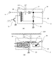
(第1の実施形態)
図1は、本発明の第1の実施形態の高圧電源の主要部分の回路図を示す。この高圧電源は、3つの高圧部ケース2a、2b、2cを備えている。3つの高圧部ケースの回路構成は基本的に同じである。
(First embodiment)
FIG. 1 shows a circuit diagram of main parts of a high-voltage power supply according to a first embodiment of the present invention. The high-voltage power supply includes three high-
高圧部ケース2a(2b、2c)は、一次側電源入力端子11a(11b、11c)を備える。一次側電源入力端子11a(11b、11c)には、例えば150Vの直流電圧が印加される。12a(12b、12c)は、プリント基板3上に実装されるFET等のトランジスタである。トランジスタ12a(12b、12c)は、例えば数10kHzの高周波で一次側電源をON/OFFするスイッチである。20a(20b、20c)はフライバックトランスである。フライバックトランス20a(20b、20c)は、トランジスタ12a(12b、12c)がONの時に蓄積されたエネルギーを、トランジスタ12a(12b、12c)がOFFの時に二次巻線から出力する。高圧ダイオード21a(21b、21c)は、フライバックトランス20a(20b、20c)の出力を整流する。コンデンサ22a(22b、22c)は、高圧ダイオード21a(21b、21c)で整流された出力を平滑する。この高圧ダイオードとコンデンサで構成される回路を整流回路とよぶ。23a(23b、23c)は二次回路の低電位側端子であり、24a(24b、24c)は二次回路の高電位側端子である。
The high-
トランス及び整流回路などの高電圧回路部分は、高圧部ケース2a(2b、2c)の外かくに覆われている。その内部は、直流電圧に対して十分な耐圧を有する絶縁性の含浸材(モールド材、封止材、充填材ともよばれる)が充填されている。含浸材としては、エポキシ樹脂等が好適である。25は高圧電源の出力端子であり、この出力端子25から表示パネル100のフェースプレートへ高電圧が供給される。
High voltage circuit parts such as a transformer and a rectifier circuit are covered outside the high
3つの高圧部ケース2a、2b、2cは直列接続される。すなわち、高圧部ケース2aの低電位側端子23aは接地電位に接続され、高電位側端子24aは高圧部ケース2bの低電位側端子23bに接続される。また、高圧部ケース2bの高電位側端子24bは高圧部ケース2cの低電位側端子23cに接続され、さらに、高圧部ケース2cの高電位側端子24cは出力端子25に接続されている。これにより、各高圧部ケースの出力電圧が合成され、目的とする高電圧を得ることができる。
Three high voltage | pressure
分圧抵抗26、27は、出力端子25の電圧を所望の割合で分圧するためのものである。分圧により得られた電位は、出力ノード28を経由して不図示の制御回路にフィードバック(負帰還)される。制御回路は、出力ノード28の電位が不図示の基準電位と等しくなるように、トランジスタ12a(12b、12c)のゲートを制御する。この構成は、トランス個々に負帰還をかける構成と比べて、トランスの一次回路と二次回路の絶縁の必要がなくなるという利点がある。また、負帰還が1系統ですむので回路構成が簡略化されるという利点も有する。なお、フィードバック制御のための制御回路は、オペアンプ等を用いて構成可能である。また、分圧抵抗26、27は、3つの高圧部ケース2a、2b、2cとは別のケースに入れ、その外かくの内部は、直流電圧に対して十分な耐圧を有する絶縁性の含浸材が充填されている構成が好適である。またこの別のケースに必要に応じてリプル電圧を減少させる目的でフィルムコンデンサ等の平滑コンデンサを並列に実装しても好適である。
The
この実施形態では、トランスを3個使用した例を示したが、トランスの数は2個であっても4個以上であっても本発明の効果は期待できる。製作コストを考慮すれば、トランスの数は10個以下が好適であった。フェースプレートに供給する電圧、電流、要求される厚みから、好適なトランスの数が決まる。本発明者らが開発している表面導電型電子放出素子を用いた画像表示装置では、高圧電源の出力電圧が12kVであり、トランスの数は3個から6個が好適であった。例えば、図1のように3個のトランスを用いる構成では、目的とする出力電圧が12kVの場合、トランス1つ当たりの出力電圧が4kVとなるように設計すればよい。 In this embodiment, an example is shown in which three transformers are used. However, the effect of the present invention can be expected even if the number of transformers is two or four or more. Considering the manufacturing cost, the number of transformers is preferably 10 or less. The number of suitable transformers is determined from the voltage, current, and required thickness supplied to the face plate. In the image display device using the surface conduction electron-emitting device developed by the present inventors, the output voltage of the high voltage power source is 12 kV, and the number of transformers is preferably 3 to 6. For example, in the configuration using three transformers as shown in FIG. 1, when the target output voltage is 12 kV, the output voltage per transformer may be designed to be 4 kV.
図1で示した構成で、交流電圧が大きいノードはノードAa点、ノードAb点、ノードAc点である。これらの点における交流電圧は、単一のトランスで昇圧する場合に比べ1/3の電圧である。すなわちコロナ放電の開始を決定する交流電圧が小さくなるため、空間距離Ld、Luを単一トランスの構成に比べ短くできる。 In the configuration shown in FIG. 1, nodes having a high AC voltage are a node Aa point, a node Ab point, and a node Ac point. The AC voltage at these points is 1/3 of the voltage boosted by a single transformer. That is, since the AC voltage that determines the start of corona discharge is reduced, the spatial distances Ld and Lu can be shortened compared to the configuration of a single transformer.
図2に本発明の第1の実施形態の高圧電源の実装形態を模式的に示す。図2の上下方向が画像表示装置の厚み方向(表示面に垂直な方向)を示しており、図2の下側が前面側、上側が背面側である。高圧電源は、フレーム200とカバー201の間に形成される空間に配置される。高圧電源は、プリント基板3と、プリント基板3に実装された3個の高圧部ケース2a、2b、2cとから構成されている。プリント基板3は、スペーサ210を介してフレーム200にネジ211で固定される。ここで、3個の高圧部ケース2a、2b、2cは、表示パネルの表示面と平行な面内に並ぶように配置されている。言い換えると、3個の高圧部ケース2a、2b、2cの厚み方向の位置が同一(若しくは実質的に同一)になるように配置される。このとき、高圧部ケース2a、2b、2cとフレーム200及びカバー201との間に所望の空間距離Ld、Luが形成されるように、スペーサ2
10の高さ及びカバー201の形状が設計されている。なお、プリント基板3において、高圧部ケース2a、2b、2cとフレーム200の間の領域には、配線などの導電部材を設けないほうがよい。なお、スペーサ210はフレーム200と別部材できている例を示したが、フレーム200の板金が部分的に折り曲げられ形成されていても良い。プリント基板3を空間距離Ld、Luが確保できる規定の位置に固定できる部材であればどのような構造であってもかまわない。
FIG. 2 schematically shows a mounting form of the high-voltage power supply according to the first embodiment of the present invention. 2 indicates the thickness direction of the image display device (direction perpendicular to the display surface). The lower side of FIG. 2 is the front side, and the upper side is the back side. The high voltage power supply is disposed in a space formed between the
The height of 10 and the shape of the
以上述べた本実施形態の構成によれば、各高圧部ケース内の交流電圧を小さくしたことで、高圧部ケースの周囲に確保すべき空間距離Ld、Luを従来よりも短くすることができる。加えて、トランスのコア断面積を小さくできるので、結果として高圧部ケース自体の小型化・薄型化も実現できる。したがって、画像表示装置の大幅な薄型化が可能となる。 According to the configuration of the present embodiment described above, the spatial distances Ld and Lu that should be secured around the high-voltage part case can be made shorter than before by reducing the AC voltage in each high-voltage part case. In addition, since the core cross-sectional area of the transformer can be reduced, as a result, the high-voltage unit case itself can be reduced in size and thickness. Therefore, the image display device can be significantly reduced in thickness.
(第2の実施形態)
図3に、本発明の第2の実施形態の高圧電源の実装形態を模式的に示す。
第2の実施形態の高圧電源の回路構成は、図1に示した第1の実施形態のものと同じである。また、図3では、第1の実施形態のものと同じ構成部分に同一の符号を付している。
(Second Embodiment)
FIG. 3 schematically shows a high voltage power supply mounting form according to the second embodiment of the present invention.
The circuit configuration of the high-voltage power supply of the second embodiment is the same as that of the first embodiment shown in FIG. Moreover, in FIG. 3, the same code | symbol is attached | subjected to the same component as the thing of 1st Embodiment.
第2の実施形態の高圧電源は、プリント基板3に複数の開口部が設けられ、各高圧部ケースが開口部内に配置されている点で、第1の実施形態と異なっている。それ以外の点では、第1の実施形態と第2の実施形態は同じである。
The high-voltage power supply of the second embodiment is different from the first embodiment in that a plurality of openings are provided in the printed
本実施形態の構成によれば、高圧部ケース2a、2b、2cとケース200の間において、比誘電率の高いプリント基板3の厚みが空間距離から除かれる。よって、第1の実施形態に比べ、さらに空間距離Ldを小さくでき、画像表示装置の一層の薄型化を図ることができる。
According to the configuration of the present embodiment, the thickness of the printed
本実施形態では、トランスを分割することにより高圧部ケースを小型化・軽量化している。これにより、図3に示すような実装形態が可能となった。すなわち、高圧部ケースが1個の場合は、必要な電力を得るため、高圧部ケースのサイズは大きく、重量は重くなる。それゆえ、強度や振動試験等の点から、プリント基板に開口部を設けるのが困難であった。これに対し、本実施形態においては、高圧部ケースが小さく且つ軽いため、プリント基板に開口部を設ける実装形態が可能となった。 In this embodiment, the high voltage | pressure part case is reduced in size and weight by dividing | segmenting a trans | transformer. Thereby, the mounting form as shown in FIG. 3 became possible. That is, when there is one high-voltage part case, the size of the high-voltage part case is large and the weight is heavy in order to obtain necessary power. Therefore, it is difficult to provide an opening in the printed circuit board from the viewpoints of strength and vibration test. On the other hand, in this embodiment, since the high-pressure part case is small and light, a mounting form in which an opening is provided in the printed circuit board is possible.
なお、プリント基板の開口部は、プリント基板の外周から切り込み部を設けた形状でも良い。すなわち、高圧部ケースとフレームの間にプリント基板が存在しない構造であれば、開口部の形状はどのようなものでもかまわない。 The opening of the printed circuit board may have a shape in which a cut portion is provided from the outer periphery of the printed circuit board. That is, as long as the printed circuit board does not exist between the high-voltage part case and the frame, the opening may have any shape.
(その他の実施形態)
上記実施形態では、フライバック型のDC/DCコンバータで昇圧を行う例を示したが、本発明はフォワード型や他の方式の回路構成にも適用可能である。整流回路として倍電圧整流回路を用いることが好ましい。高圧電源の出力電圧に対して交流電圧を小さくでき、空間距離を小さくできるからである。
(Other embodiments)
In the above embodiment, an example is shown in which boosting is performed by a flyback type DC / DC converter, but the present invention can also be applied to forward and other circuit configurations. A voltage doubler rectifier circuit is preferably used as the rectifier circuit. This is because the AC voltage can be reduced relative to the output voltage of the high-voltage power supply, and the spatial distance can be reduced.
上記実施形態では、各高圧部ケースの中に1つずつトランスを実装しているが、各高圧部ケースの中に、直列接続した2つ以上のトランスを実装することも可能である。高圧部ケースの数を少なくすれば、コストを下げる効果がある。 In the above-described embodiment, one transformer is mounted in each high-voltage unit case, but it is also possible to mount two or more transformers connected in series in each high-voltage unit case. Reducing the number of high-pressure part cases has the effect of reducing costs.
上記実施形態では、導電性材料からなるカバー201を用いたが、樹脂製のカバーを用
いることもできる。その場合、樹脂製のカバーと高圧電源の間に、導体のシールド板を設けると良い。このとき、高圧部ケースとシールド板の間の距離が所望の空間距離Luを満足するように設計する。
In the above embodiment, the
上記実施形態では、複数の高圧部ケースが1次元的に配列されているが、表示パネルの表示面と平行な面内に2次元的に配列してもよい。ここで「表示面と平行な面」とは、厳密に(数学的、幾何学的に)平行な面だけでなく、実質的に平行な面をも含む。例えば、物理的な制約や意匠的な制約から、フレーム200に凹凸があったり、フレーム200と表示面とが若干傾斜していたりすると、高圧部ケースを表示面に対して厳密に平行に配置することが難しい場合がある。しかし、複数の高圧部ケースが概ね表示面に平行に並んでいれば、本発明の目的である薄型化の要求は達成できる。したがって、「表示面と平行な面」は「表示面に沿った面」を意味するものということができる。
In the above embodiment, the plurality of high-voltage unit cases are arranged one-dimensionally, but they may be arranged two-dimensionally in a plane parallel to the display surface of the display panel. Here, the “surface parallel to the display surface” includes not only a strictly (mathematical and geometric) parallel surface but also a substantially parallel surface. For example, if the
上記実施形態では、表面導電型電子放出素子を使用した画像表示装置に本発明を適用した例を説明したが、本発明は、高電圧を必要とするあらゆる平面型画像表示装置に適用可能である。 In the above embodiment, the example in which the present invention is applied to the image display device using the surface conduction electron-emitting device has been described. However, the present invention is applicable to any flat image display device that requires a high voltage. .
また、本発明の別の効果として、同じ構成の高圧部ケースを複数使用するため、量産効果でコストを下げることが期待できる。また高圧部ケース等のメンテナンス用部品も小さなものになり管理費用も安くなる。 Further, as another effect of the present invention, since a plurality of high-pressure part cases having the same configuration are used, it can be expected to reduce the cost due to the mass production effect. In addition, maintenance parts such as a high-pressure part case are small, and the management cost is low.
1・・・高圧電源、2a,2b,2c・・・高圧部ケース、100・・・表示パネル、200・・・フレーム、201・・・カバー
DESCRIPTION OF
Claims (6)
各ケースが1つ以上のトランスと整流回路を内蔵する複数のケースを備え、該複数のケースを直列接続することにより前記高電圧を得るものであり、
前記複数のケースは、前記フレームと前記カバーの間に形成される空間に、前記表示パネルの表示面と平行な面内に並ぶように配置されている
ことを特徴とする高圧電源。 In a flat image display device comprising a flat display panel, a frame attached to the back side of the display panel, and a cover that covers at least the back side of the frame, for applying a high voltage to the display panel A high voltage power supply,
Each case includes a plurality of cases containing one or more transformers and a rectifier circuit, and the high voltage is obtained by connecting the plurality of cases in series,
The plurality of cases are arranged in a space formed between the frame and the cover so as to be arranged in a plane parallel to the display surface of the display panel.
ことを特徴とする請求項1又は2に記載の高圧電源。 A voltage dividing resistor for dividing the high voltage output from the high voltage power supply, and a control circuit for controlling the output voltage of each case by feeding back a potential obtained by the voltage division. Item 3. The high-voltage power source according to item 1 or 2 .
前記プリント基板は、開口部を有しており、
前記各ケースは、前記開口部内に配置されて、前記プリント基板に実装される
ことを特徴とする請求項1〜3のいずれかに記載の高圧電源。 Having a printed circuit board attached to the frame via a spacer;
The printed circuit board has an opening,
Each case is disposed in the opening, high-voltage power supply according to claim 1, characterized in that it is mounted on the printed circuit board.
ことを特徴とする請求項1〜4のいずれかに記載の高圧電源。 The high-voltage power supply according to any one of claims 1 to 4 , wherein the inside of the case is filled with an insulating impregnation material.
前記表示パネルの背面側に取り付けられるフレームと、 A frame attached to the back side of the display panel;
前記フレームの背面側を少なくとも覆うカバーと、 A cover covering at least the back side of the frame;
前記表示パネルに高電圧を印加する高圧電源と、を備える平面型画像表示装置であって、 A flat-type image display device comprising a high-voltage power supply for applying a high voltage to the display panel,
前記高圧電源が、請求項1〜5のいずれかに記載の高圧電源である The high-voltage power supply is the high-voltage power supply according to any one of claims 1 to 5.
ことを特徴とする平面型画像表示装置。A flat-type image display device.
Priority Applications (4)
| Application Number | Priority Date | Filing Date | Title |
|---|---|---|---|
| JP2009175626A JP5289225B2 (en) | 2009-07-28 | 2009-07-28 | Flat panel display, high voltage power supply |
| EP10168844A EP2282623A2 (en) | 2009-07-28 | 2010-07-08 | Flat display apparatus and high-voltage power supply |
| US12/835,851 US8542493B2 (en) | 2009-07-28 | 2010-07-14 | Flat display apparatus and high-voltage power supply |
| CN2010102373696A CN101986377A (en) | 2009-07-28 | 2010-07-23 | Flat display apparatus and high-voltage power supply |
Applications Claiming Priority (1)
| Application Number | Priority Date | Filing Date | Title |
|---|---|---|---|
| JP2009175626A JP5289225B2 (en) | 2009-07-28 | 2009-07-28 | Flat panel display, high voltage power supply |
Publications (3)
| Publication Number | Publication Date |
|---|---|
| JP2011028109A JP2011028109A (en) | 2011-02-10 |
| JP2011028109A5 JP2011028109A5 (en) | 2012-08-30 |
| JP5289225B2 true JP5289225B2 (en) | 2013-09-11 |
Family
ID=43066538
Family Applications (1)
| Application Number | Title | Priority Date | Filing Date |
|---|---|---|---|
| JP2009175626A Expired - Fee Related JP5289225B2 (en) | 2009-07-28 | 2009-07-28 | Flat panel display, high voltage power supply |
Country Status (4)
| Country | Link |
|---|---|
| US (1) | US8542493B2 (en) |
| EP (1) | EP2282623A2 (en) |
| JP (1) | JP5289225B2 (en) |
| CN (1) | CN101986377A (en) |
Families Citing this family (4)
| Publication number | Priority date | Publication date | Assignee | Title |
|---|---|---|---|---|
| JP2013062896A (en) * | 2011-09-12 | 2013-04-04 | Rohm Co Ltd | Power supply circuit |
| CN103326612B (en) * | 2013-06-18 | 2015-09-16 | 中国科学院电工研究所 | A kind of unipolarity microsecond pulse high voltage source |
| WO2016066187A1 (en) * | 2014-10-28 | 2016-05-06 | Abb Technology Ltd | Power converter assembly with insulating material-covered electrodes |
| CN107801342B (en) * | 2017-11-24 | 2024-01-26 | 珠海格力电器股份有限公司 | Support structure of electric appliance component, circuit component and device with electric appliance component |
Family Cites Families (20)
| Publication number | Priority date | Publication date | Assignee | Title |
|---|---|---|---|---|
| CN1060171A (en) * | 1990-09-25 | 1992-04-08 | 丁定藩 | Adopt the driver and the driving circuit of the plasma scope of low back voltage transistor |
| JPH04167409A (en) | 1990-10-30 | 1992-06-15 | Mitsubishi Electric Corp | Flyback transformer |
| JPH08130867A (en) * | 1994-10-31 | 1996-05-21 | Canon Inc | High voltage generator |
| WO2000060568A1 (en) | 1999-04-05 | 2000-10-12 | Canon Kabushiki Kaisha | Electron source and image forming device |
| WO2000060569A1 (en) | 1999-04-05 | 2000-10-12 | Canon Kabushiki Kaisha | Electron source and image forming device |
| JP2002156938A (en) | 2000-11-21 | 2002-05-31 | Canon Inc | Image display device and its driving method |
| US7079161B2 (en) | 2001-06-14 | 2006-07-18 | Canon Kabushiki Kaisha | Image display apparatus |
| KR100840235B1 (en) * | 2001-08-29 | 2008-06-20 | 삼성전자주식회사 | Liquid crystal display device |
| JP3893341B2 (en) | 2001-09-28 | 2007-03-14 | キヤノン株式会社 | Image display device and method for adjusting image display device |
| US6952193B2 (en) | 2001-12-12 | 2005-10-04 | Canon Kabushiki Kaisha | Image display apparatus and image display methods |
| US7102701B2 (en) * | 2001-12-27 | 2006-09-05 | Canon Kabushiki Kaisha | Display device |
| JP2005019685A (en) | 2003-06-26 | 2005-01-20 | Sony Corp | Transformer and high voltage generator |
| JP4252471B2 (en) * | 2004-02-09 | 2009-04-08 | 株式会社 日立ディスプレイズ | Image display device |
| JP4194567B2 (en) | 2004-02-27 | 2008-12-10 | キヤノン株式会社 | Image display device |
| JP2006156092A (en) | 2004-11-29 | 2006-06-15 | Canon Inc | Image display device using high voltage |
| JP2007187981A (en) * | 2006-01-16 | 2007-07-26 | Toshiba Matsushita Display Technology Co Ltd | Display device |
| JP2007206261A (en) * | 2006-01-31 | 2007-08-16 | Toshiba Corp | Display device |
| JP2008004323A (en) | 2006-06-21 | 2008-01-10 | Hitachi Displays Ltd | Image display device |
| JP4143658B2 (en) | 2006-07-05 | 2008-09-03 | キヤノン株式会社 | Image display device |
| CN201051193Y (en) * | 2006-10-25 | 2008-04-23 | 深圳市赛其创新科技有限公司 | Power circuit of backlight display system |
-
2009
- 2009-07-28 JP JP2009175626A patent/JP5289225B2/en not_active Expired - Fee Related
-
2010
- 2010-07-08 EP EP10168844A patent/EP2282623A2/en not_active Withdrawn
- 2010-07-14 US US12/835,851 patent/US8542493B2/en not_active Expired - Fee Related
- 2010-07-23 CN CN2010102373696A patent/CN101986377A/en active Pending
Also Published As
| Publication number | Publication date |
|---|---|
| US20110025672A1 (en) | 2011-02-03 |
| JP2011028109A (en) | 2011-02-10 |
| EP2282623A2 (en) | 2011-02-09 |
| CN101986377A (en) | 2011-03-16 |
| US8542493B2 (en) | 2013-09-24 |
Similar Documents
| Publication | Publication Date | Title |
|---|---|---|
| JP5289225B2 (en) | Flat panel display, high voltage power supply | |
| EP0404022A2 (en) | Flat configuration image display apparatus and manufacturing method thereof | |
| US7372438B2 (en) | Electroluminescent display | |
| JP5490994B2 (en) | X-ray generator | |
| TW513734B (en) | Display apparatus | |
| US7102701B2 (en) | Display device | |
| JP2007109603A (en) | Image display device | |
| US20040085307A1 (en) | Aging apparatus of field emission device and method thereof | |
| JP2008041539A (en) | Spontaneous light emitting display device | |
| US7834535B2 (en) | Flat panel type display apparatus | |
| US8513868B2 (en) | Display panel, display apparatus, television apparatus, and method of producing the display panel | |
| JP3768877B2 (en) | Display device | |
| JP2007025330A (en) | Display panel structure body and display apparatus using the same | |
| JP3768878B2 (en) | Display device | |
| US7221086B2 (en) | Display device including a shield member | |
| JP2006004807A (en) | Flat-surface display device | |
| EP1522085B1 (en) | Matrix display device | |
| JP5213631B2 (en) | Image display device | |
| JP2006172890A (en) | Image display device | |
| JP2007086642A (en) | Image display device | |
| WO2006006470A1 (en) | Image display device | |
| JP2003198987A (en) | Display | |
| JPH1173893A (en) | Field emission suppressing device | |
| JPH1092344A (en) | Cathode ray tube and cathode ray tube device | |
| JP2006093051A (en) | Image display apparatus |
Legal Events
| Date | Code | Title | Description |
|---|---|---|---|
| A521 | Written amendment |
Free format text: JAPANESE INTERMEDIATE CODE: A523 Effective date: 20120713 |
|
| A621 | Written request for application examination |
Free format text: JAPANESE INTERMEDIATE CODE: A621 Effective date: 20120713 |
|
| TRDD | Decision of grant or rejection written | ||
| A977 | Report on retrieval |
Free format text: JAPANESE INTERMEDIATE CODE: A971007 Effective date: 20130430 |
|
| A01 | Written decision to grant a patent or to grant a registration (utility model) |
Free format text: JAPANESE INTERMEDIATE CODE: A01 Effective date: 20130507 |
|
| A61 | First payment of annual fees (during grant procedure) |
Free format text: JAPANESE INTERMEDIATE CODE: A61 Effective date: 20130604 |
|
| LAPS | Cancellation because of no payment of annual fees |