JP5284415B2 - Flip-flop circuit device and processor device using the same - Google Patents
Flip-flop circuit device and processor device using the same Download PDFInfo
- Publication number
- JP5284415B2 JP5284415B2 JP2011125500A JP2011125500A JP5284415B2 JP 5284415 B2 JP5284415 B2 JP 5284415B2 JP 2011125500 A JP2011125500 A JP 2011125500A JP 2011125500 A JP2011125500 A JP 2011125500A JP 5284415 B2 JP5284415 B2 JP 5284415B2
- Authority
- JP
- Japan
- Prior art keywords
- flip
- latch circuit
- circuit
- side terminal
- output
- Prior art date
- Legal status (The legal status is an assumption and is not a legal conclusion. Google has not performed a legal analysis and makes no representation as to the accuracy of the status listed.)
- Expired - Fee Related
Links
- 238000012546 transfer Methods 0.000 claims description 14
- 238000012545 processing Methods 0.000 claims description 11
- 230000000295 complement effect Effects 0.000 claims description 8
- 230000003014 reinforcing effect Effects 0.000 claims description 2
- 230000005540 biological transmission Effects 0.000 description 50
- 238000010586 diagram Methods 0.000 description 42
- 238000000034 method Methods 0.000 description 42
- 230000008569 process Effects 0.000 description 42
- 230000008878 coupling Effects 0.000 description 36
- 238000010168 coupling process Methods 0.000 description 36
- 238000005859 coupling reaction Methods 0.000 description 36
- 238000006880 cross-coupling reaction Methods 0.000 description 12
- HCUOEKSZWPGJIM-YBRHCDHNSA-N (e,2e)-2-hydroxyimino-6-methoxy-4-methyl-5-nitrohex-3-enamide Chemical compound COCC([N+]([O-])=O)\C(C)=C\C(=N/O)\C(N)=O HCUOEKSZWPGJIM-YBRHCDHNSA-N 0.000 description 9
- MZAGXDHQGXUDDX-JSRXJHBZSA-N (e,2z)-4-ethyl-2-hydroxyimino-5-nitrohex-3-enamide Chemical compound [O-][N+](=O)C(C)C(/CC)=C/C(=N/O)/C(N)=O MZAGXDHQGXUDDX-JSRXJHBZSA-N 0.000 description 9
- 101001109689 Homo sapiens Nuclear receptor subfamily 4 group A member 3 Proteins 0.000 description 9
- 101000598778 Homo sapiens Protein OSCP1 Proteins 0.000 description 9
- 101001067395 Mus musculus Phospholipid scramblase 1 Proteins 0.000 description 9
- 102100022673 Nuclear receptor subfamily 4 group A member 3 Human genes 0.000 description 9
- 230000014759 maintenance of location Effects 0.000 description 9
- 230000004048 modification Effects 0.000 description 9
- 238000012986 modification Methods 0.000 description 9
- 230000003247 decreasing effect Effects 0.000 description 5
- 230000004044 response Effects 0.000 description 4
- 238000004088 simulation Methods 0.000 description 3
- 230000015572 biosynthetic process Effects 0.000 description 2
- 230000001934 delay Effects 0.000 description 2
- 238000000926 separation method Methods 0.000 description 2
- 230000003068 static effect Effects 0.000 description 2
- 238000003786 synthesis reaction Methods 0.000 description 2
- 230000008859 change Effects 0.000 description 1
- 230000006866 deterioration Effects 0.000 description 1
- 230000007274 generation of a signal involved in cell-cell signaling Effects 0.000 description 1
- 230000007257 malfunction Effects 0.000 description 1
- 229910044991 metal oxide Inorganic materials 0.000 description 1
- 150000004706 metal oxides Chemical class 0.000 description 1
- 230000006855 networking Effects 0.000 description 1
- 230000003071 parasitic effect Effects 0.000 description 1
- 230000002250 progressing effect Effects 0.000 description 1
- 239000004065 semiconductor Substances 0.000 description 1
Images

Description
本発明は、特に、安定に低電圧動作可能なフリップフロップ回路装置及びそれを用いたプロセッサ装置に関する。 The present invention particularly relates to a flip-flop circuit device capable of stably operating at a low voltage and a processor device using the flip-flop circuit device.
昨今、LSIで構成されたプロセッサ装置において、マルチコア化が進んでいる。しかしながら、すべてのコアを使い切ることは難しいという問題点があった。以下の明細書において、「ハイアクティブ」とは、ハイレベル信号の論理が真論理を表す(ポジティブ・トゥルー(positive-true))論理回路、信号処理回路又はプロセッサをいい、「ローアクティブ」とは、ローレベル信号の論理が真論理を表す(ネガティブ・トゥルー(negative-true))論理回路、信号処理回路又はプロセッサをいう。また、pチャンネルMOS(Metal-Oxide Semiconductor)トランジスタをpMOSトランジスタといい。nチャンネルMOSトランジスタをnMOSトランジスタという。 In recent years, multi-core processing is progressing in processor devices composed of LSIs. However, there is a problem that it is difficult to use all the cores. In the following description, “high active” means a logic circuit, signal processing circuit or processor in which the logic of a high level signal represents true logic (positive-true), and “low active” means , A logic circuit, signal processing circuit or processor in which the logic of a low level signal represents true logic (negative-true). A p-channel MOS (Metal-Oxide Semiconductor) transistor is called a pMOS transistor. The n-channel MOS transistor is called an nMOS transistor.
本発明者らは、プロセッサ装置において、使用していないコアのリソースを使用して低電圧動作できないか検討してきた。プロセッサ装置において、低電圧動作で問題になるのはフリップフロップ回路であり、その故障原因について以下のように検討した。 The present inventors have examined whether or not a low-voltage operation can be performed by using unused core resources in a processor device. In the processor device, it is the flip-flop circuit that becomes a problem in the low voltage operation, and the cause of the failure was examined as follows.
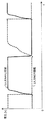
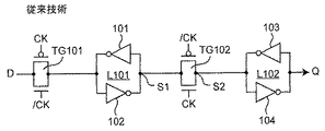
図16は、例えばプロセッサ装置で用いられる、従来技術に係る一般的なマスタスレーブ型フリップフロップ回路の構成を示す回路図である(例えば、特許文献3参照。)。図16において、入力端子と出力端子との間に、伝送ゲートTG101と、クロスカップリングされたインバータ101,102からなるラッチ回路L101と、伝送ゲートTG102と、クロスカップリングされたインバータ103,104からなるラッチ回路L102とを備えて構成される。ここで、入力信号Dを入力したときに、ラッチ回路L101からの出力信号をS1とし、伝送ゲートTG102からの出力信号をS2とし、ラッチ回路L102からの出力信号であって当該フリップフロップ回路の出力信号をQとする。
FIG. 16 is a circuit diagram showing the configuration of a general master-slave flip-flop circuit according to the prior art used in, for example, a processor device (see, for example, Patent Document 3). In FIG. 16, a transmission gate TG101, a latch circuit L101 including
図17は図16のフリップフロップ回路の低電圧動作時の問題点を示す信号波形図である。図17から明らかなように、各ラッチ回路L101,L102からの出力信号S1,Qにおいて、符号301及び302で示すように、レベル保持力(リテンション)が弱く、信号レベルが低下して誤動作する場合があるという問題点があった。
FIG. 17 is a signal waveform diagram showing problems in the low-voltage operation of the flip-flop circuit of FIG. As is apparent from FIG. 17, in the output signals S1 and Q from the latch circuits L101 and L102, as indicated by
本発明の目的は以上の問題点を解決し、従来技術に比較して低電圧で安定に動作することができるフリップフロップ回路装置とそれを用いたプロセッサ装置を提供することにある。 An object of the present invention is to solve the above problems and provide a flip-flop circuit device that can operate stably at a lower voltage than the prior art and a processor device using the flip-flop circuit device.
第1の発明に係るフリップフロップ回路装置は、
それぞれ入力側端子及び出力側端子を有する第1のラッチ回路と第2のラッチ回路とを第1のゲートを介して接続して構成された第1のフリップフロップ回路と、
それぞれ入力側端子及び出力側端子を有する第3のラッチ回路と第4のラッチ回路とを第2のゲートを介して接続して構成された第2のフリップフロップ回路と、
上記第1のラッチ回路の入力側端子と、上記第3のラッチ回路の出力側端子との間を短絡又は開放し、短絡時に同一の論理値を有する第3のゲートと、
上記第1のラッチ回路の出力側端子と、上記第3のラッチ回路の入力側端子との間を短絡又は開放し、短絡時に同一の論理値を有する第4のゲートと、
上記第2のラッチ回路の入力側端子と、上記第4のラッチ回路の出力側端子との間を短絡又は開放し、短絡時に同一の論理値を有する第5のゲートと、
上記第2のラッチ回路の出力側端子と、上記第4のラッチ回路の入力側端子との間を短絡又は開放し、短絡時に同一の論理値を有する第6のゲートとを備えたフリップフロップ回路装置であって、
所定の第1の動作電圧で動作させる第1の電圧モード時に、上記第3乃至第6のゲートを開放することにより上記第1のフリップフロップ回路と上記第2のフリップフロップ回路とを別々に動作させる一方、上記第1の動作電圧よりも低い第2の動作電圧で動作させる第2の電圧モード時に、上記第3乃至第6のゲートを短絡することにより上記第1のフリップフロップ回路と上記第2のフリップフロップ回路とを互いに反転関係のデータを保持して相補的なデータ処理を行うように協働動作させることを特徴とする。
The flip-flop circuit device according to the first invention is
A first flip-flop circuit configured by connecting a first latch circuit and an second latch circuit each having an input-side terminal and an output-side terminal via a first gate;
A second flip-flop circuit configured by connecting a third latch circuit and an fourth latch circuit each having an input side terminal and an output side terminal via a second gate;
A third gate that short-circuits or opens between the input-side terminal of the first latch circuit and the output-side terminal of the third latch circuit, and has the same logical value when short-circuited;
A fourth gate that short-circuits or opens between the output-side terminal of the first latch circuit and the input-side terminal of the third latch circuit, and has the same logical value when short-circuited;
A fifth gate that short-circuits or opens between the input-side terminal of the second latch circuit and the output-side terminal of the fourth latch circuit, and has the same logical value when short-circuited;
A flip-flop circuit comprising a sixth gate that short-circuits or opens between the output-side terminal of the second latch circuit and the input-side terminal of the fourth latch circuit and has the same logical value when short-circuited A device,
The first flip-flop circuit and the second flip-flop circuit are operated separately by opening the third to sixth gates in the first voltage mode for operating at a predetermined first operating voltage. On the other hand, the second flip-flop circuit and the first flip-flop circuit are short-circuited by short-circuiting the third to sixth gates in the second voltage mode in which the second operating voltage is lower than the first operating voltage. The two flip-flop circuits are operated in a cooperative manner so as to hold complementary data and perform complementary data processing.
上記フリップフロップ回路装置において、上記第1のフリップフロップ回路は、上記第1のラッチ回路に記憶されたデータを所定の転送期間において上記第1のゲートを介して上記第2のラッチ回路に転送して出力し、
上記第2のフリップフロップ回路は、上記第3のラッチ回路に記憶されたデータを上記転送期間において上記第2のゲートを介して上記第4のラッチ回路に転送して出力することにより、上記第1のフリップフロップ回路とは互いに反転関係のデータを保持し、
上記第3のゲートは、上記第1のラッチ回路の入力側端子と、上記第3のラッチ回路の出力側端子との間に接続されかつ上記第1のラッチ回路の入力側端子と上記第3のラッチ回路の出力側端子との間を短絡又は開放し、上記短絡時に上記第1のラッチ回路の入力側端子及び上記第3のラッチ回路の出力側端子において同一の論理値を有し、
上記第4のゲートは、上記第1のラッチ回路の出力側端子と、上記第3のラッチ回路の入力側端子との間に接続されかつ上記第1のラッチ回路の出力側端子と上記第3のラッチ回路の入力側端子との間を短絡又は開放し、上記短絡時に上記第1のラッチ回路の出力側端子及び上記第3のラッチ回路の入力側端子において同一の論理値を有し、
上記第5のゲートは、上記第2のラッチ回路の入力側端子と、上記第4のラッチ回路の出力側端子との間に接続されかつ上記第2のラッチ回路の入力側端子と上記第4のラッチ回路の出力側端子との間を短絡又は開放し、上記短絡時に上記第2のラッチ回路の入力側端子及び上記第4のラッチ回路の出力側端子において同一の論理値を有し、
上記第6のゲートは、上記第2のラッチ回路の出力側端子と、上記第4のラッチ回路の入力側端子との間に接続されかつ上記第2のラッチ回路の出力側端子と上記第4のラッチ回路の入力側端子との間を短絡又は開放し、上記短絡時に上記第2のラッチ回路の出力側端子及び上記第4のラッチ回路の入力側端子において同一の論理値を有することを特徴とする。
In the flip-flop circuit device, the first flip-flop circuit transfers the data stored in the first latch circuit to the second latch circuit through the first gate in a predetermined transfer period. Output,
The second flip-flop circuit transfers the data stored in the third latch circuit to the fourth latch circuit via the second gate and outputs the data in the transfer period, whereby the second flip-flop circuit outputs the data. 1 flip-flop circuit holds data in an inversion relationship with each other,
The third gate is connected between the input-side terminal of the first latch circuit and the output-side terminal of the third latch circuit, and the input-side terminal of the first latch circuit and the third gate Between the output side terminal of the first latch circuit and the output side terminal of the third latch circuit at the time of the short circuit,
The fourth gate is connected between the output-side terminal of the first latch circuit and the input-side terminal of the third latch circuit, and the output-side terminal of the first latch circuit and the third gate Between the input side terminals of the first latch circuit and the input side terminals of the third latch circuit at the time of the short circuit, and having the same logical value,
The fifth gate is connected between the input side terminal of the second latch circuit and the output side terminal of the fourth latch circuit, and the input side terminal of the second latch circuit and the fourth gate. Between the output side terminal of the second latch circuit and the output side terminal of the fourth latch circuit at the time of the short circuit,
The sixth gate is connected between the output side terminal of the second latch circuit and the input side terminal of the fourth latch circuit, and the output side terminal of the second latch circuit and the fourth gate. And the output side terminal of the second latch circuit and the input side terminal of the fourth latch circuit have the same logical value at the time of the short circuit. And
また、上記フリップフロップ回路装置において、上記第1のラッチ回路はクロスカップリングされた第1及び第2のインバータを含み、
上記第2のラッチ回路はクロスカップリングされた第3及び第4のインバータを含み、
上記第3のラッチ回路はクロスカップリングされた第5及び第6のインバータを含み、
上記第4のラッチ回路はクロスカップリングされた第7及び第8のインバータを含み、
上記第2の電圧モード時に、上記第6のインバータからの出力信号を上記第1のインバータからの出力信号により同一の論理値で補強して上記第1のラッチ回路の出力側端子からの出力信号の信号保持力を増大させ、上記第2のインバータからの出力信号を上記第5のインバータからの出力信号により同一の論理値で補強して上記第3のラッチ回路の出力側端子からの出力信号の信号保持力を増大させ、
上記第2の電圧モード時に、上記第8のインバータからの出力信号を上記第3のインバータからの出力信号により同一の論理値で補強して上記第2のラッチ回路の出力側端子からの出力信号の信号保持力を増大させ、上記第4のインバータからの出力信号を上記第7のインバータからの出力信号により同一の論理値で補強して上記第4のラッチ回路の出力側端子からの出力信号の信号保持力を増大させることを特徴とする。
In the flip-flop circuit device, the first latch circuit includes first and second inverters that are cross-coupled.
The second latch circuit includes third and fourth inverters that are cross-coupled,
The third latch circuit includes fifth and sixth inverters that are cross-coupled,
The fourth latch circuit includes seventh and eighth inverters that are cross-coupled,
In the second voltage mode, the output signal from the sixth inverter is reinforced with the same logical value by the output signal from the first inverter, and the output signal from the output side terminal of the first latch circuit Output signal from the output terminal of the third latch circuit by reinforcing the output signal from the second inverter with the same logic value by the output signal from the fifth inverter. Increase the signal holding power of
In the second voltage mode, the output signal from the eighth inverter is reinforced with the same logical value by the output signal from the third inverter, and the output signal from the output side terminal of the second latch circuit And the output signal from the fourth inverter is reinforced with the same logical value by the output signal from the seventh inverter, and the output signal from the output side terminal of the fourth latch circuit. It is characterized in that the signal holding power of the is increased.
さらに、上記フリップフロップ回路装置において、上記第1のインバータの出力電力を上記第6のインバータの出力電力よりも大きくなるように設定し、
上記第5のインバータの出力電力を上記第2のインバータの出力電力よりも大きくなるように設定し、
上記第3のインバータの出力電力を上記第8のインバータの出力電力よりも大きくなるように設定し、
上記第7のインバータの出力電力を上記第4のインバータの出力電力よりも大きくなるように設定したことを特徴とする。
Further, in the flip-flop circuit device, the output power of the first inverter is set to be larger than the output power of the sixth inverter,
Setting the output power of the fifth inverter to be larger than the output power of the second inverter;
The output power of the third inverter is set to be larger than the output power of the eighth inverter,
The output power of the seventh inverter is set to be larger than the output power of the fourth inverter.
またさらに、上記フリップフロップ回路装置において、上記第1のフリップフロップ回路及び上記第2のフリップフロップ回路はそれぞれ、マスタスレーブ型フリップフロップ回路であることを特徴とする。 Further, in the flip-flop circuit device, the first flip-flop circuit and the second flip-flop circuit are each a master-slave type flip-flop circuit.
またさらに、上記フリップフロップ回路装置は、上記第1のフリップフロップ回路及び上記第2のフリップフロップ回路はそれぞれ、センスアンプ型フリップフロップ回路であることを特徴とする。 Still further, the flip-flop circuit device is characterized in that each of the first flip-flop circuit and the second flip-flop circuit is a sense amplifier type flip-flop circuit.
第2の発明に係るプロセッサ装置は、上記フリップフロップ回路装置を備えたことを特徴とする。 A processor device according to a second aspect of the present invention includes the flip-flop circuit device.
従って、本発明によれば、所定の第1の動作電圧で動作させる第1の電圧モード時に、上記第3乃至第6のゲートを開放することにより上記第1のフリップフロップ回路と上記第2のフリップフロップ回路とを別々に動作させる一方、上記第1の動作電圧よりも低い第2の動作電圧で動作させる第2の電圧モード時に、上記第3乃至第6のゲートを短絡することにより上記第1のフリップフロップ回路と上記第2のフリップフロップ回路とを互いに反転関係のデータを保持して相補的なデータ処理を行うように協働動作させる。すなわち、2種類の動作モードを有し、例えば所定の標準電圧では一般的なフリップフロップ回路と同様に動作する一方、例えば低電圧モードでは、2つのフリップフロップ回路の内部ノードを接続し、フリップフロップ回路装置の容量は半分になるが低電圧で動作することができる。ここで、低電圧モードでは、分離されたフリップフロップ回路の各ラッチ回路においてデータの保持力を小さいが、内部ノードを接続することで相補的にデータの保持力を増大させて動作させることができる。 Therefore, according to the present invention, the first flip-flop circuit and the second flip-flop circuit are opened by opening the third to sixth gates in the first voltage mode for operating at a predetermined first operating voltage. While the flip-flop circuit is operated separately, the third to sixth gates are short-circuited in a second voltage mode in which the flip-flop circuit is operated at a second operating voltage lower than the first operating voltage. One flip-flop circuit and the second flip-flop circuit are cooperatively operated so as to hold complementary data and perform complementary data processing. That is, it has two types of operation modes, for example, operates in the same manner as a general flip-flop circuit at a predetermined standard voltage, while, for example, in the low-voltage mode, the internal nodes of the two flip-flop circuits are connected to each other. Although the capacity of the circuit device is halved, it can operate at a low voltage. Here, in the low voltage mode, the data holding power is small in each latch circuit of the separated flip-flop circuit, but it can be operated by complementaryly increasing the data holding power by connecting the internal nodes. .
実施形態.
以下、本発明に係る実施形態について図面を参照して説明する。なお、以下の各実施形態において、同様の構成要素については同一の符号を付している。
Embodiment.
Hereinafter, embodiments according to the present invention will be described with reference to the drawings. In addition, in each following embodiment, the same code | symbol is attached | subjected about the same component.
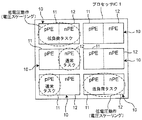
図1は本発明の一実施形態に係る、複数のコアを有するプロセッサIC1の構成を示すブロック図である。図1において、プロセッサIC1(プロセッサ装置)は複数のコア10を備えて構成され、各コア10は、ハイアクティブで動作するポジティブ・トゥルーのプロセッサエレメント(以下、pPEという。)11と、ローアクティブで動作するネガティブ・トゥルーのプロセッサエレメント(以下、nPEという。)12とを互いに隣接して配置するように備えて構成される。多くのコアアーキテクチャでは、処理を実行するために十分なプロセッサエレメント(以下、PEという。)が存在する。低負荷タスクでは、一般的に、すべてのPEを必要とされない。低いプロセッサ利用率よりは、低電力が望まれている。このような条件のもとでは、余分なハードウエアのリソースを活用して消費電力を節約することができる。ここで、2つのPEに対して積極的に最低動作電圧(Vmin)を低下させることができ、低消費電力化に有効である。
FIG. 1 is a block diagram showing a configuration of a
図1のプロセッサIC1において、通常のタスクは、pPE11又はnPE12のいずれかで定格電圧で実行される。一方、低負荷のタスクでは、上記定格電圧よりも低い電圧(電圧スケーリング)で動作可能なカップリングプロセッサ(pPE11とnPE12との1対)を構成する。本発明者らはこれを「プロセッサ・カップリング・アーキテクチャ」と呼び、高い負荷を、高い周波数(速度ブースティング)で動作するカップリングプロセッサに割り当てる。 In the processor IC1 of FIG. 1, normal tasks are performed at rated voltage on either pPE11 or nPE12. On the other hand, in a low-load task, a coupling processor (a pair of pPE11 and nPE12) that can operate at a voltage (voltage scaling) lower than the rated voltage is configured. We refer to this as a “processor coupling architecture” and assign a high load to a coupling processor operating at a high frequency (speed boosting).
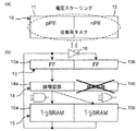
図2Aは図1のコア10においていわゆるハイアクティブのパスが選択された場合であって、電圧スケーリング(低負荷タスクの実行)時のコア10とその等価回路を示すブロック図である。図2Bは図1のコア10においていわゆるハイアクティブのパスが選択された場合であって、速度ブースティング(高負荷タスクの実行)時のコア10とその等価回路を示すブロック図である。すなわち、図2A及び図2Bは、上述のプロセッサ・カップリング・アーキテクチャにおける2つのタイプの構成(電圧スケーリング及び速度ブースティング)を示している。図2A及び図2Bにおいて、16はインバータであり、pPE及びnPEからなるコア10は、
(a)2個のフリップフロップ回路13a,13bからなるフリップフロップ回路部13と、
(b)2個の論理回路14a,14bからなる論理回路部14と、
(c)2個の1/2SRAM15a,15bからなるSRAM(Static Random Access Memory)15と
を含み等価的に構成される。ここで、pPE11は、フリップフロップ回路13aと、論理回路14aと、1/2SRAM15aとの構成に対応し、nPE12は、フリップフロップ回路13bと、論理回路14bと、1/2SRAM15bとの構成に対応する。
FIG. 2A is a block diagram showing the
(A) a flip-
(B) a
(C) An SRAM (Static Random Access Memory) 15 composed of two 1/2
図2A及び図2Bから明らかなように、論理回路14において、ハイアクティブのパス又はローアクティブのパスのいずれかがプロセスバラツキに依存して選択されるが、両方の1/2SRAM15a,15bが使用される。なぜならば、SRAM15は、低電圧動作又は高周波動作に応じて半分に分割されている。電圧スケーリングでは、カップリングされたフリップフロップ回路部13(詳細後述する)が低電圧動作を確実に実行するために提供されている。
As apparent from FIGS. 2A and 2B, in the
図3は図1及び図2のコア10において用いる7T/14TカップリングSRAMの構成を示す回路図である。すなわち、図3は、非特許文献2において開示された2つのビットセルに対して14個のトランジスタ(14T)を有するカップリングSRAMビットセルを示す。
FIG. 3 is a circuit diagram showing a configuration of a 7T / 14T coupling SRAM used in the
図3において、MOSトランジスタM00,M02にてなるインバータ21と、MOSトランジスタM01,M03にてなるインバータ22とがクロスカップリングされて第1のラッチ回路L1を構成する。ラッチ回路L1のノードN00はMOSトランジスタM04を介してビット線BLに接続され、ラッチ回路L1のノードN01はMOSトランジスタM05を介して反転ビット線/BLに接続される。ここで、MOSトランジスタM04,M05の各ゲートはワード線WL0に接続される。また、MOSトランジスタM10,M12にてなるインバータ23と、MOSトランジスタM11,M13にてなるインバータ24とがクロスカップリングされて第2のラッチ回路L2を構成する。ラッチ回路L2のノードN10はMOSトランジスタM14を介してビット線BLに接続され、ラッチ回路L2のノードN11はMOSトランジスタM15を介して反転ビット線/BLに接続される。ここで、MOSトランジスタM14,M15の各ゲートはワード線WL1に接続される。さらに、ノードN00は伝送ゲートであるMOSトランジスタM20を介してノード10に接続され、ノードN01は伝送ゲートであるMOSトランジスタM21を介してノード11に接続される。ここで、制御線信号/CTRLがローレベルとなると、MOSトランジスタM20及びM21がオンされ、2つのビットセルが同一の論理値で接続されてカップリング状態となる。
In FIG. 3, an
以上のように構成されたカップリングSRAMにおいて、2個のpMOSトランジスタM20,M21が、従来技術に係る6トランジスタ(以下、6Tという。)ビットセルの1対における内部ノードN01,N11に接続されている。7T/14T SRAMは以下の3つのモードを有する。
(1)ノーマルモード(7T):制御線信号/CTRLがハイレベルとされて付加的なMOSトランジスタM20,M21がオフされる。7Tの各ビットセルは、従来技術の6Tセルとして動作する。
(2)電圧スケーリングモード(低電圧モードともいう。)(14T):制御線信号/CTRLがローレベルとされて付加的なMOSトランジスタM20,M21がオンされる。ここで、内部ノードM20,M21はメモリセルのペアで共用されるが、ワード線WL0又はWL1のいずれかがアサートされる。そのように構成することにより、アクセストランジスタに対する駆動トランジスタのサイズ比である比βが2倍になるので、より大きな静雑音マージンを得ることができる。
(3)速度ブースティングモード(14T):付加的なMOSトランジスタM20,M21がオフされる。両方のワード線WL0,WL1は駆動され、14個のトランジスタを用いてより高速で読み出し動作を行うことができる。昨今のプロセッサ装置では、動作周波数を制限するので、メモリのアクセス時間は非常に重要である(例えば、非特許文献2参照。)。
In the coupling SRAM configured as described above, two pMOS transistors M20 and M21 are connected to internal nodes N01 and N11 in a pair of 6-transistor (hereinafter referred to as 6T) bit cells according to the prior art. . The 7T / 14T SRAM has the following three modes.
(1) Normal mode (7T): The control line signal / CTRL is set to the high level, and the additional MOS transistors M20 and M21 are turned off. Each 7T bit cell operates as a prior art 6T cell.
(2) Voltage scaling mode (also referred to as low voltage mode) (14T): The control line signal / CTRL is set to low level, and the additional MOS transistors M20 and M21 are turned on. Here, although the internal nodes M20 and M21 are shared by a pair of memory cells, either the word line WL0 or WL1 is asserted. With such a configuration, the ratio β, which is the size ratio of the drive transistor to the access transistor, is doubled, so that a larger static noise margin can be obtained.
(3) Speed boosting mode (14T): Additional MOS transistors M20 and M21 are turned off. Both word lines WL0 and WL1 are driven, and a read operation can be performed at a higher speed using 14 transistors. In recent processor devices, the operating frequency is limited, so the memory access time is very important (see, for example, Non-Patent Document 2).
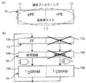
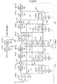
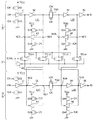
図4Aは図1及び図2のコア10において用いるマスタスレーブ型カップリングフリップフロップ回路の第1の部分の構成を示す回路図である。また、図4Bは図1及び図2のコア10において用いるマスタスレーブ型カップリングフリップフロップ回路の第2の部分の構成を示す回路図である。さらに、図4Cは図4Bの入力信号回路部36で用いる制御線信号CTRL1,CTRL2,CTRL3に基づいて制御する非制御伝送ゲート、及び各モードに対するオンオフ制御を示す表である。
FIG. 4A is a circuit diagram showing the configuration of the first part of the master-slave coupling flip-flop circuit used in the
図4A及び図4Bにおいて、マスタスレーブ型カップリングフリップフロップ回路は、
(1)クロックCLKに基づいて制御クロック信号CK,/CK(以下、CK信号、/CK信号という。)を発生するCK信号発生部30と、
(2)電圧スケーリングモードにおいて、入力信号D,/Dに基づいて、内部処理用入力信号Din,/Dinを発生する入力信号回路部36と、
(3)入力信号Dinを所定時間だけ遅延させて出力信号Qを発生して出力するフリップフロップ回路FF1と、
(4)入力信号/Dinを所定時間だけ遅延させて出力信号/Qを発生して出力するフリップフロップ回路FF2と、
(5)動作モードを示す制御線信号CTRL1,CTRL2,CTRL3に応じてフリップフロップ回路FF1,FF2を互いにカップリングさせるか否かを選択的に切り換えるゲート回路部37とを備えて構成される。ここで、後者3つの回路でFF回路部35を構成する。
4A and 4B, the master-slave coupling flip-flop circuit is
(1) a CK signal generator 30 that generates control clock signals CK and / CK (hereinafter referred to as CK signal and / CK signal) based on the clock CLK;
(2) In the voltage scaling mode, based on the input signals D and / D, the input signal circuit unit 36 that generates the internal processing input signals Din and / Din;
(3) a flip-flop circuit FF1 that delays the input signal Din by a predetermined time to generate and output the output signal Q;
(4) a flip-flop circuit FF2 that delays the input signal / Din by a predetermined time to generate and output the output signal / Q;
(5) A
図4AのCK信号発生部30は、2個のMOSトランジスタQ1,Q2からなるインバータ31と、2個のMOSトランジスタQ3,Q4からなるインバータ32とが縦続接続されて構成され、インバータ31はクロックCLKを反転して/CK信号を発生してインバータ32に出力し、インバータ32は/CK信号を反転してCK信号を発生して出力する。
The CK signal generation unit 30 in FIG. 4A is configured by cascading an
図4Bの入力信号回路部36は、
(1)CK信号及び/CK信号に応答してオン又はオフとなる伝送ゲートTG3,TG4と、
(2)動作モードを示す制御線信号/CTRL及びそれがインバータ40aにより反転された制御線信号CTRLに応答してオン又はオフとなる伝送ゲートTG5,TG6と、
(3)MOSトランジスタQ5,Q6からなるインバータ33と、
(4)MOSトランジスタQ7,Q8からなるインバータ34とを備えて構成される。
The input signal circuit unit 36 in FIG.
(1) transmission gates TG3 and TG4 that are turned on or off in response to the CK signal and the / CK signal;
(2) transmission line TG5, TG6 that is turned on or off in response to the control line signal / CTRL indicating the operation mode and the control line signal CTRL inverted by the
(3) an
(4) An
以上のように構成された入力信号回路部36の動作について、図4B及び図4Cを参照して以下説明する。各伝送ゲートTG3〜TG6については、動作モードに応じて変化する3つの制御線信号CTRL1,CTRL2,CTRL3に基づいてオンオフ制御される。 The operation of the input signal circuit unit 36 configured as described above will be described below with reference to FIGS. 4B and 4C. The transmission gates TG3 to TG6 are on / off controlled based on three control line signals CTRL1, CTRL2, and CTRL3 that change according to the operation mode.
電圧スケーリングモード(低電圧モード)の入力信号D選択モードでは、伝送ゲートTG3,TG5,TG6がオンとされ、伝送ゲートTG4がオフとされ、入力信号Dは伝送ゲートTG3を介して、入力信号Dinとして図4Aのフリップフロップ回路FF1に入力されるとともに、伝送ゲートTG3からインバータ33、及び伝送ゲートTG5を介して入力信号/Dinとしてフリップフロップ回路FF2に入力される。
In the input signal D selection mode of the voltage scaling mode (low voltage mode), the transmission gates TG3, TG5 and TG6 are turned on, the transmission gate TG4 is turned off, and the input signal D is input to the input signal Din via the transmission gate TG3. 4A is input to the flip-flop circuit FF1 from the transmission gate TG3 through the
また、電圧スケーリングモード(低電圧モード)の入力信号/D選択モードでは、伝送ゲートTG4,TG5,TG6がオンとされ、伝送ゲートTG3がオフとされ、入力信号/Dは伝送ゲートTG4を介して、入力信号/Dinとして図4Aのフリップフロップ回路FF2に入力されるとともに、伝送ゲートTG4からインバータ34、及び伝送ゲートTG6を介して入力信号Dinとしてフリップフロップ回路FF1に入力される。
In the input signal / D selection mode of the voltage scaling mode (low voltage mode), the transmission gates TG4, TG5 and TG6 are turned on, the transmission gate TG3 is turned off, and the input signal / D is transmitted via the transmission gate TG4. The input signal / Din is input to the flip-flop circuit FF2 of FIG. 4A, and is input from the transmission gate TG4 to the flip-flop circuit FF1 as the input signal Din via the
さらに、速度ブースティングモード又はFF分離モード(フリップフロップ回路FF1とFF2を分離して独立して動作させるモードをいう。)では、伝送ゲートTG3,TG4がオンとされ、伝送ゲートTG5,TG6がオフとされ、入力信号Dは伝送ゲートTG3を介して、入力信号Dinとして図4Aのフリップフロップ回路FF1に入力されるとともに、入力信号/Dは伝送ゲートTG4を介して、入力信号/Dinとして図4Aのフリップフロップ回路FF2に入力される。 Furthermore, in the speed boosting mode or the FF separation mode (a mode in which the flip-flop circuits FF1 and FF2 are separated and operated independently), the transmission gates TG3 and TG4 are turned on and the transmission gates TG5 and TG6 are turned off. The input signal D is input to the flip-flop circuit FF1 of FIG. 4A through the transmission gate TG3 as the input signal Din, and the input signal / D is input as the input signal / Din through the transmission gate TG4 as shown in FIG. 4A. To the flip-flop circuit FF2.
すなわち、2つのフリップフロップ回路FF1,FF2がカップリングしないときは(電圧スケーリングモード以外の速度ブースティングモード又はFF分離モードなどの動作モード)、伝送ゲートTG5,TG6がオフとされ、入力信号Dから内部処理用入力信号Dinまでに至るラインLN1と、入力信号/Dから内部処理用入力信号/Dinまでに至るラインLN2とが分離され、2つのフリップフロップ回路FF1,FF2が別々に動作する。一方、電圧スケーリングモードにおいて、伝送ゲートTG5,TG6がオンとされて上述のように動作する。 That is, when the two flip-flop circuits FF1 and FF2 are not coupled (operation mode such as speed boosting mode or FF separation mode other than the voltage scaling mode), the transmission gates TG5 and TG6 are turned off, and the input signal D The line LN1 extending to the internal processing input signal Din and the line LN2 extending from the input signal / D to the internal processing input signal / Din are separated, and the two flip-flop circuits FF1 and FF2 operate separately. On the other hand, in the voltage scaling mode, the transmission gates TG5 and TG6 are turned on and operate as described above.
次いで、図4Aのフリップフロップ回路FF1,FF2の構成及び動作について以下に説明する。 Next, the configuration and operation of the flip-flop circuits FF1 and FF2 in FIG. 4A will be described below.
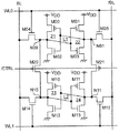
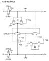
図4Aのフリップフロップ回路FF1は、
(1)MOSトランジスタQ11〜Q14からなるインバータ41と、
(2)MOSトランジスタQ15,Q16からなるインバータ42と、
(3)MOSトランジスタQ17〜Q20からなるインバータ43と、
(4)転送ゲートTG1と、
(5)MOSトランジスタQ21,Q22からなるインバータ44と、
(6)MOSトランジスタQ23〜Q26からなるインバータ45と、
(7)MOSトランジスタQ27,Q28からなるインバータ46とを備えて構成される。ここで、インバータ42とインバータ43とが互いにクロスカップリングされてラッチ回路L11を構成し、インバータ44とインバータ45とが互いにクロスカップリングされてラッチ回路L12を構成する。そして、インバータ41と、ラッチ回路L11と、伝送ゲートTG1と、ラッチ回路L12と、インバータ46とがこれらの順序で縦続接続されてフリップフロップ回路FF1を構成する。なお、インバータ41,43,45において、CK信号,/CK信号に応じて動作するMOSトランジスタQ12,Q13,Q18,Q19,Q24,Q25を挿入しているのは、インバータ41,43,45の非動作時(データ信号を保持せず、伝送するとき)において各インバータの入出力間を遮断してデータ信号の伝送を遮断して、データ信号を伝達するためである。
The flip-flop circuit FF1 in FIG.
(1) an
(2) an
(3) an
(4) transfer gate TG1,
(5) an
(6) an
(7) An
図4Aのフリップフロップ回路FF2は、
(1)MOSトランジスタQ31〜Q34からなるインバータ51と、
(2)MOSトランジスタQ35,Q36からなるインバータ52と、
(3)MOSトランジスタQ37〜Q40からなるインバータ53と、
(4)転送ゲートTG2と、
(5)MOSトランジスタQ41,Q42からなるインバータ54と、
(6)MOSトランジスタQ43〜Q46からなるインバータ55と、
(7)MOSトランジスタQ47,Q48からなるインバータ56とを備えて構成される。ここで、インバータ52とインバータ53とが互いにクロスカップリングされてラッチ回路L21を構成し、インバータ54とインバータ55とが互いにクロスカップリングされてラッチ回路L22を構成する。そして、インバータ51と、ラッチ回路L21と、伝送ゲートTG2と、ラッチ回路L22と、インバータ56とがこれらの順序で縦続接続されてフリップフロップ回路FF2を構成する。なお、インバータ51,53,55において、CK信号,/CK信号に応じて動作するMOSトランジスタQ32,Q33,Q38,Q39,Q44,Q45を挿入しているのは、インバータ51,53,55の非動作時(データ信号を保持せず、伝送するとき)において各インバータの入出力間を遮断してデータ信号の伝送を遮断して、データ信号を伝達するためである。
The flip-flop circuit FF2 in FIG.
(1) an
(2) an
(3) an
(4) transfer gate TG2,
(5) an
(6) an
(7) An
図4Aのゲート回路35は4個の伝送ゲートTG11〜TG14とインバータ40とを備えて構成され、電圧スケーリングモードのときに、制御線信号/CTRLがローレベルとなり、これらの伝送ゲートTG11〜TG14がオンとされて、内部ノードN21と内部ノードN32が接続され、内部ノードN22と内部ノードN31が接続され、内部ノードN23と内部ノードN34が接続され、内部ノードN24と内部ノードN33が接続される。これにより、2個のフリップフロップ回路FF1,FF2がカップリングして、ラッチ回路L11とL21で同一の論理値のデータを保持し、ラッチ回路L12とL22で同一の論理値のデータを保持することにより、時間経過によって信号レベルが低下することを防止して、データ信号の保持力を増大させることができる。
4A includes four transmission gates TG11 to TG14 and an
図4Aの回路では、例えば、以下のようにして、所定の占有エリアで構成した場合において、小さい出力電力のノードにおけるデータ信号を、それよりも大きな出力電力のノードにおけるデータ信号により補強することでデータ信号の保持力を増大させることができる。 In the circuit shown in FIG. 4A, for example, in the case where the circuit is configured in a predetermined occupation area as described below, the data signal at the node having the smaller output power is reinforced by the data signal at the node having the larger output power. The holding power of the data signal can be increased.
(1)インバータ42の各MOSトランジスタQ15,Q16のゲート長をインバータ53の各MOSトランジスタQ37〜Q40のゲート長よりも長くすることにより、インバータ42の出力端子から出力される出力電力を、インバータ53の出力端子から出力される出力電力よりも大きく設計して設定することができる。
(2)インバータ52の各MOSトランジスタQ35,Q36のゲート長をインバータ43の各MOSトランジスタQ17〜Q20のゲート長よりも長くすることにより、インバータ52の出力端子から出力される出力電力を、インバータ43の出力端子から出力される出力電力よりも大きく設計して設定することができる。
(3)インバータ44の各MOSトランジスタQ21,Q22のゲート長をインバータ55の各MOSトランジスタQ43〜Q46のゲート長よりも長くすることにより、インバータ44の出力端子から出力される出力電力を、インバータ55の出力端子から出力される出力電力よりも大きく設計して設定することができる。
(4)インバータ54の各MOSトランジスタQ41,Q42のゲート長をインバータ45の各MOSトランジスタQ23〜Q26のゲート長よりも長くすることにより、インバータ54の出力端子から出力される出力電力を、インバータ45の出力端子から出力される出力電力よりも大きく設計して設定することができる。
(1) By making the gate lengths of the MOS transistors Q15 and Q16 of the
(2) By making the gate lengths of the MOS transistors Q35 and Q36 of the
(3) By making the gate lengths of the MOS transistors Q21 and Q22 of the
(4) By making the gate lengths of the MOS transistors Q41 and Q42 of the
以上のように構成された図4A及び図4Bのマスタスレーブ型カップリングフリップフロップ回路において、不平衡なFSプロセスコーナー(nMOSトランジスタが高速(Fast)で制御されかつpMOSトランジスタが低速(Slow)で制御されてシミュレーションされるプロセスコーナーをいう。また、nMOSトランジスタが低速(Slow)で制御されかつpMOSトランジスタが高速(Fast)で制御されてシミュレーションされるプロセスコーナーをSFプロセスコーナーという。詳細は図5参照。)は、図4Aのラッチ回路L11,L12のデータ信号の信号保持力が臨界的であるために、所定の低電圧動作において臨界的なプロセスコーナーとなる。このことは、6T SRAMにおける最悪の信号保持力の状態と同様である。 4A and 4B configured as described above, the unbalanced FS process corner (the nMOS transistor is controlled at a high speed (Fast) and the pMOS transistor is controlled at a low speed (Slow)). A process corner that is simulated by controlling the nMOS transistor at a low speed (Slow) and a pMOS transistor at a high speed (Fast) is referred to as an SF process corner. .) Is a critical process corner in a predetermined low-voltage operation because the signal holding power of the data signals of the latch circuits L11 and L12 in FIG. 4A is critical. This is the same as the worst signal retention state in 6T SRAM.
なお、FSプロセスコーナー及びSFプロセスコーナー以外のプロセスコーナーを以下のように定義する。
(a)SSプロセスコーナー:nMOSトランジスタが低速(Slow)で制御されかつpMOSトランジスタが低速(Slow)で制御されてシミュレーションされるプロセスコーナーをいう。
(b)TTプロセスコーナー:nMOSトランジスタが典型値(Typical)で制御されかつpMOSトランジスタが典型値(Typical)で制御されてシミュレーションされるプロセスコーナーをいう。
(c)FFプロセスコーナー:nMOSトランジスタが高速(Fast)で制御されかつpMOSトランジスタが高速(Fast)で制御されてシミュレーションされるプロセスコーナーをいう。
The process corners other than the FS process corner and the SF process corner are defined as follows.
(A) SS process corner: A process corner which is simulated by controlling the nMOS transistor at a low speed (Slow) and controlling the pMOS transistor at a low speed (Slow).
(B) TT process corner: A process corner which is simulated by controlling the nMOS transistor at a typical value and controlling the pMOS transistor at a typical value.
(C) FF process corner: A process corner in which an nMOS transistor is controlled at high speed (Fast) and a pMOS transistor is controlled at high speed (Fast).
本実施形態に係るカップリングされたフリップフロップ回路において、内部ノードが上述のように4個の伝送ゲートTG11〜TG14を用いて接続され、このとき、2個のフリップフロップ回路FF1,FF2は互いに同一の論理値を有する各データ信号を補強しあう。これら伝送ゲートTG11〜TG14は、動作モードに従って変化する制御線信号/CTRLによって適応的に切り換えられ、例えば、ノーマルモードでは、伝送ゲートTG11〜TG14がともにオフとされて、上記2個のフリップフロップ回路FF1,FF2は独立して動作することができる。 In the coupled flip-flop circuit according to the present embodiment, the internal nodes are connected using the four transmission gates TG11 to TG14 as described above, and at this time, the two flip-flop circuits FF1 and FF2 are identical to each other. Reinforce each data signal having a logical value of. These transmission gates TG11 to TG14 are adaptively switched by a control line signal / CTRL that changes according to the operation mode. For example, in the normal mode, both the transmission gates TG11 to TG14 are turned off, and the two flip-flop circuits FF1 and FF2 can operate independently.
本発明者らが行った65nmプロセスによるシミュレーションでは、上記FSプロセスコーナーで製造された1個のフリップフロップ回路FF1又はFF2の最低動作電圧Vminは0.46Vであり、上記カップリングされたフリップフロップ回路では、0.27Vまで低下させることができる。これは、上記カップリングされたフリップフロップ回路はデータ保持力の特性を大幅に改善できるためである。上述した電圧スケーリングモードは、例えば、バイオメディカルセンシング、センサネットワーキング、及びウエラブルコンピューティングなどの極めて低電力のアプリケーションに対して適用することができる。 In the simulation by the 65 nm process performed by the present inventors, the minimum operating voltage Vmin of one flip-flop circuit FF1 or FF2 manufactured at the FS process corner is 0.46 V, and the coupled flip-flop circuit is Then, it can be reduced to 0.27V. This is because the coupled flip-flop circuit can greatly improve the characteristics of data retention. The voltage scaling mode described above can be applied to very low power applications such as biomedical sensing, sensor networking, and wearable computing.
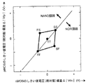
図5は図2A及び図2Bの論理回路14a,14bにおいてプロセスコーナーを変化したときのnMOSのしきい値電圧(絶対値)偏差Δ|Vtn|(V)とpMOSのしきい値電圧(絶対値)偏差Δ|Vtp|(V)との関係を示す図である。図5において、5つのプロセスコーナーを示している。通常、論理回路合成の場合のために、SSプロセスコーナー、TTプロセスコーナー及びFFプロセスコーナーについて考える。上述したように、最悪のプロセスコーナーは非常に低電源電圧で不平衡なコーナーである。図5において、1つのプロセスコーナーと好ましい論理ゲートとの関係を示している。
FIG. 5 shows the threshold voltage (absolute value) deviation Δ | Vtn | (V) of the nMOS and the threshold voltage (absolute value) of the pMOS when the process corner is changed in the
図6Aはコア10のデコーダ回路のうちNAND回路部の構成を示す回路図であり、図6Bはコア10のデコーダ回路のうちNOR回路部の構成を示す回路図である。また、図7Aは図6AのナンドゲートNAND1〜3の詳細構成を示す回路図であり、図7Bは図6BのノアゲートNOR1〜3の詳細構成を示す回路図である。さらに、図8Aは図7AのナンドゲートNAND1〜3及び図7BのノアゲートNOR1〜3をSFプロセスコーナーで試作したときの各出力信号の波形図であり、図8Bは図7AのナンドゲートNAND1〜3及び図7BのノアゲートNOR1〜3をFSプロセスコーナーで試作したときの各出力信号の波形図である。
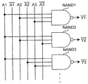
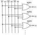
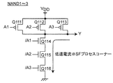
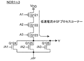
6A is a circuit diagram showing the configuration of the NAND circuit portion in the decoder circuit of the core 10, and FIG. 6B is a circuit diagram showing the configuration of the NOR circuit portion in the decoder circuit of the
図6AのNAND回路部は、3個のナンドゲートNAND1〜NAND3を備えて構成され、各ナンドゲートNAND1〜NAND3は図7Aのごとく3個のpMOSトランジスタQ111〜Q113及びnMOSトランジスタQ114〜Q116を備えて構成される。この場合においては、図7Aにおいて3入力NANDゲートがスタックされた3個のnMOSトランジスタQ114〜Q116を有するために、図8Aに示すように、SFプロセスコーナーで比較的長い立下り時間を有する。 6A includes three NAND gates NAND1 to NAND3, and each NAND gate NAND1 to NAND3 includes three pMOS transistors Q111 to Q113 and nMOS transistors Q114 to Q116 as illustrated in FIG. 7A. The In this case, since three nMOS transistors Q114 to Q116 are stacked in FIG. 7A with three input NAND gates, as shown in FIG. 8A, a relatively long fall time is provided at the SF process corner.
また、図6BのNOR回路部は、3個のノアゲートNOR1〜NOR3を備えて構成され、各ノアゲートNOR1〜NOR3は図7Bのごとく3個のpMOSトランジスタQ121〜Q123及びnMOSトランジスタQ124〜Q126を備えて構成される。この場合においては、図7Bにおいて3入力NORゲートがスタックされた3個のpMOSトランジスタQ121〜Q123を有するために、図8Bに示すように、FSプロセスコーナーで比較的長い立ち上り時間を有する。 6B includes three NOR gates NOR1 to NOR3, and each NOR gate NOR1 to NOR3 includes three pMOS transistors Q121 to Q123 and nMOS transistors Q124 to Q126 as shown in FIG. 7B. Composed. In this case, since there are three pMOS transistors Q121 to Q123 stacked in FIG. 7B with three-input NOR gates, as shown in FIG. 8B, it has a relatively long rise time at the FS process corner.
本実施形態においては、すべてのデータパスが二重になっているので、プロセスのバラツキに応じてよりよいデータパスを選択することができる(図2A、図2B参照。)。 In this embodiment, since all the data paths are duplicated, a better data path can be selected according to process variations (see FIGS. 2A and 2B).
変形例.
図9は本発明の第1の変形例に係るマスタスレーブ型カップリングフリップフロップ回路の構成を示す回路図である。なお、図4Bの入力信号回路部36は図9〜図11の回路の前段に設けられる。
Modified example.
FIG. 9 is a circuit diagram showing a configuration of a master-slave coupling flip-flop circuit according to a first modification of the present invention. Note that the input signal circuit section 36 in FIG. 4B is provided in the previous stage of the circuits in FIGS.
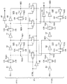
図9において、本発明の第1の変形例に係るマスタスレーブ型カップリングフリップフロップ回路は、2個のフリップフロップ回路FF11,FF12と、図4Aと同様の構成を有するゲート回路部37とを備えて構成される。フリップフロップ回路FF11は、MOSトランジスタQ12,Q13,Q18,Q19,Q24,Q25と、インバータ41〜46と、伝送ゲートTG1とを備えて構成される。ここで、クロスカップリングで接続された2個のインバータ42,43によりラッチ回路L31を構成し、クロスカップリングで接続された2個のインバータ44,45によりラッチ回路L32を構成する。また、フリップフロップ回路FF12は、MOSトランジスタQ32,Q33,Q38,Q39,Q44,Q45と、インバータ51〜56と、伝送ゲートTG2とを備えて構成される。ここで、クロスカップリングで接続された2個のインバータ52,53によりラッチ回路L41を構成し、クロスカップリングで接続された2個のインバータ54,55によりラッチ回路L42を構成する。
9, the master-slave coupling flip-flop circuit according to the first modification of the present invention includes two flip-flop circuits FF11 and FF12, and a
以上のように構成された図9のマスタスレーブ型カップリングフリップフロップ回路においても、図4Aのカップリングフリップフロップ回路と同様に、2つのフリップフロップ回路FF11,FF12が動作モードに応じてカップリングされ又はカップリングされてないで動作することができる。ここで、カップリングさせる電圧スケーリングモードのときに、制御線信号/CTRLがローレベルとなり、これらの伝送ゲートTG11〜TG14がオンとされて、内部ノードN21と内部ノードN32が接続され、内部ノードN22と内部ノードN31が接続され、内部ノードN23と内部ノードN34が接続され、内部ノードN24と内部ノードN33が接続される。これにより、2個のフリップフロップ回路FF11,FF12がカップリングして、ラッチ回路L31とL41で同一の論理値のデータを保持し、ラッチ回路L32とL42で同一の論理値のデータを保持することにより、時間経過によって信号レベルが低下することを防止して、データ信号の保持力を増大させることができる。 In the master-slave coupling flip-flop circuit of FIG. 9 configured as described above, the two flip-flop circuits FF11 and FF12 are coupled according to the operation mode, similarly to the coupling flip-flop circuit of FIG. 4A. Or it can operate without being coupled. Here, in the voltage scaling mode for coupling, the control line signal / CTRL becomes low level, the transmission gates TG11 to TG14 are turned on, the internal node N21 and the internal node N32 are connected, and the internal node N22 is connected. And the internal node N31, the internal node N23 and the internal node N34 are connected, and the internal node N24 and the internal node N33 are connected. As a result, the two flip-flop circuits FF11 and FF12 are coupled so that the latch circuits L31 and L41 hold the same logical value data, and the latch circuits L32 and L42 hold the same logical value data. Thus, it is possible to prevent the signal level from decreasing with the passage of time, and to increase the retention of the data signal.
図10は本発明の第2の変形例に係るマスタスレーブ型カップリングフリップフロップ回路の構成を示す回路図である。 FIG. 10 is a circuit diagram showing a configuration of a master-slave coupling flip-flop circuit according to a second modification of the present invention.
図10において、本発明の第2の変形例に係るマスタスレーブ型カップリングフリップフロップ回路は、2個のフリップフロップ回路FF21,FF22と、図4Aと同様の構成を有するゲート回路部37とを備えて構成される。フリップフロップ回路FF21は、インバータ41〜48(46を除く)と、伝送ゲートTG1,TG21〜TG23とを備えて構成される。ここで、クロスカップリングで接続された2個のインバータ42,43によりラッチ回路L51を構成し、クロスカップリングで接続された2個のインバータ44,45によりラッチ回路L52を構成する。また、フリップフロップ回路FF22は、インバータ51〜58(56を除く)と、伝送ゲートTG2,TG31〜TG33とを備えて構成される。ここで、クロスカップリングで接続された2個のインバータ52,53によりラッチ回路L61を構成し、クロスカップリングで接続された2個のインバータ54,55によりラッチ回路L62を構成する。
10, the master-slave coupling flip-flop circuit according to the second modification of the present invention includes two flip-flop circuits FF21 and FF22, and a
図10のマスタスレーブ型カップリングフリップフロップ回路においても、図4Aのカップリングフリップフロップ回路と同様に、2つのフリップフロップ回路FF21,FF22が動作モードに応じてカップリングされ又はカップリングされてないで動作することができる。ここで、カップリングさせる電圧スケーリングモードのときに、制御線信号/CTRLがローレベルとなり、これらの伝送ゲートTG11〜TG14がオンとされて、内部ノードN21と内部ノードN32が接続され、内部ノードN22と内部ノードN31が接続され、内部ノードN23と内部ノードN34が接続され、内部ノードN24と内部ノードN33が接続される。これにより、2個のフリップフロップ回路FF21,FF22がカップリングして、ラッチ回路L51とL61で同一の論理値のデータを保持し、ラッチ回路L52とL62で同一の論理値のデータを保持することにより、時間経過によって信号レベルが低下することを防止して、データ信号の保持力を増大させることができる。 In the master-slave type coupling flip-flop circuit of FIG. 10 as well, the two flip-flop circuits FF21 and FF22 are not coupled or not coupled depending on the operation mode, similarly to the coupling flip-flop circuit of FIG. 4A. Can work. Here, in the voltage scaling mode for coupling, the control line signal / CTRL becomes low level, the transmission gates TG11 to TG14 are turned on, the internal node N21 and the internal node N32 are connected, and the internal node N22 is connected. And the internal node N31, the internal node N23 and the internal node N34 are connected, and the internal node N24 and the internal node N33 are connected. As a result, the two flip-flop circuits FF21 and FF22 are coupled, and the latch circuits L51 and L61 hold the same logical value data, and the latch circuits L52 and L62 hold the same logical value data. Thus, it is possible to prevent the signal level from decreasing with the passage of time, and to increase the retention of the data signal.
図11は本発明の第3の変形例に係るセンスアンプ型カップリングフリップフロップ回路の構成を示す回路図である。 FIG. 11 is a circuit diagram showing a configuration of a sense amplifier type coupling flip-flop circuit according to a third modification of the present invention.
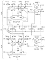
図11において、本発明の第3の変形例に係るセンスアンプ型カップリングフリップフロップ回路は、2個のフリップフロップ回路FF31,FF32と、図4Aと同様の構成を有するゲート回路部37とを備えて構成される。
11, the sense amplifier type coupling flip-flop circuit according to the third modification of the present invention includes two flip-flop circuits FF31 and FF32 and a
フリップフロップ回路FF31は、MOSトランジスタQ61〜Q70と、インバータ60と、NANDゲートNAND11,NAND12とを備えて構成される。ここで、MOSトランジスタQ61及びQ62によりCMOSインバータ61を構成し、MOSトランジスタQ63及びQ64によりCMOSインバータ62を構成し、クロスカップリングで接続された2個のCMOSインバータ61,62によりラッチ回路L71を構成し、クロスカップリングで接続された2個のNANDゲートNAND11,NAND12によりラッチ回路L72を構成する。なお、初段のラッチ回路L71の第1の内部ノードN21から出力される信号PはナンドゲートNAND12の第2の入力端子に入力され、初段のラッチ回路L71の第2の内部ノードN22から出力される信号/PはナンドゲートNAND11の第1の入力端子に入力される。
The flip-flop circuit FF31 includes MOS transistors Q61 to Q70, an
フリップフロップ回路FF32は、MOSトランジスタQ71〜Q80と、インバータ70と、NANDゲートNAND21,NAND22とを備えて構成される。ここで、MOSトランジスタQ71及びQ72によりCMOSインバータ71を構成し、MOSトランジスタQ73及びQ74によりCMOSインバータ72を構成し、クロスカップリングで接続された2個のCMOSインバータ71,72によりラッチ回路L81を構成し、クロスカップリングで接続された2個のNANDゲートNAND21,NAND22によりラッチ回路L82を構成する。なお、初段のラッチ回路L81の第1の内部ノードN31から出力される信号/PはナンドゲートNAND22の第2の入力端子に入力され、初段のラッチ回路L81の第2の内部ノードN32から出力される信号PはナンドゲートNAND21の第1の入力端子に入力される。
The flip-flop circuit FF32 includes MOS transistors Q71 to Q80, an
以上のように構成された図11のセンスアンプ型カップリングフリップフロップ回路においても、図4Aのカップリングフリップフロップ回路と同様に、2つのフリップフロップ回路FF31,FF32が動作モードに応じてカップリングされ又はカップリングされてないで動作することができる。ここで、カップリングさせる電圧スケーリングモードのときに、制御線信号/CTRLがローレベルとなり、これらの伝送ゲートTG11〜TG14がオンとされて、内部ノードN21と内部ノードN32が接続され、内部ノードN22と内部ノードN31が接続され、内部ノードN23と内部ノードN34が接続され、内部ノードN24と内部ノードN33が接続される。これにより、2個のフリップフロップ回路FF31,FF32がカップリングして、ラッチ回路L71とL81で同一の論理値のデータを保持し、ラッチ回路L72とL82で同一の論理値のデータを保持することにより、時間経過によって信号レベルが低下することを防止して、データ信号の保持力を増大させることができる。 In the sense amplifier type coupling flip-flop circuit of FIG. 11 configured as described above, the two flip-flop circuits FF31 and FF32 are coupled according to the operation mode, similarly to the coupling flip-flop circuit of FIG. 4A. Or it can operate without being coupled. Here, in the voltage scaling mode for coupling, the control line signal / CTRL becomes low level, the transmission gates TG11 to TG14 are turned on, the internal node N21 and the internal node N32 are connected, and the internal node N22 is connected. And the internal node N31, the internal node N23 and the internal node N34 are connected, and the internal node N24 and the internal node N33 are connected. Thereby, the two flip-flop circuits FF31 and FF32 are coupled, and the latch circuits L71 and L81 hold the same logical value data, and the latch circuits L72 and L82 hold the same logical value data. Thus, it is possible to prevent the signal level from decreasing with the passage of time, and to increase the retention of the data signal.
さらに、図4A、図4B、図10、図11の伝送ゲートTG1〜TG33に代わる変形例について以下に説明する。 Furthermore, a modified example of the transmission gates TG1 to TG33 shown in FIGS. 4A, 4B, 10 and 11 will be described below.
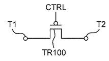
図12は図4A、図4B、図10、図11の伝送ゲートTG1〜TG33に代わる変形例である転送ゲートTR100の構成を示す回路図である。すなわち、上記伝送ゲートTG1〜TG33に代えて、端子T1,T2を有する図12の転送ゲートTR100を使用してもよい。 FIG. 12 is a circuit diagram showing a configuration of a transfer gate TR100 which is a modified example in place of the transmission gates TG1 to TG33 of FIGS. 4A, 4B, 10 and 11. That is, instead of the transmission gates TG1 to TG33, the transfer gate TR100 of FIG. 12 having terminals T1 and T2 may be used.
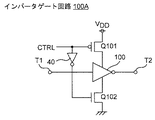
図13は図4A、図4B、図10、図11の伝送ゲートTG1〜TG33に代わる変形例であるインバータゲート回路100Aの構成を示す回路図である。上記伝送ゲートTG1〜TG33に代えて、端子T1,T2を有する図13のインバータゲート回路100Aを使用してもよい。ここで、インバータゲート回路100Aは、インバータ100と、インバータ100の電源制御用MOSトランジスタQ101,Q102と、制御線信号CTRLを反転するインバータ40とを備えて構成される。
FIG. 13 is a circuit diagram showing a configuration of an inverter gate circuit 100A which is a modified example in place of the transmission gates TG1 to TG33 of FIGS. 4A, 4B, 10 and 11. Instead of the transmission gates TG1 to TG33, the inverter gate circuit 100A of FIG. 13 having terminals T1 and T2 may be used. Here, the inverter gate circuit 100A includes an
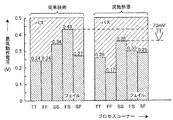
図14は従来技術に係るフリップフロップ回路及び実施形態に係るフリップフロップ回路のシミュレーション結果であって、各プロセスコーナーに対する1MHz動作時の最低動作電圧を示すグラフである。図14から明らかなように、ワーストであったFSプロセスコーナーでの最低動作電圧が0.43Vから0.30Vに改善され、SSプロセスコーナーがワーストになり0.34Vから0.36Vに悪化している。ただ、SSプロセスコーナーの場合には、2ビットのカップリングにする必要はないので、プロセスコーナーごとにカップリング/非カップリングを選択すればよい。なお、TTプロセスコーナー、SSプロセスコーナー及びSFプロセスコーナーの遅延の悪化は、追加回路の寄生容量の増加に伴う遅延の増大によるものと考えられる。 FIG. 14 is a graph showing the simulation result of the flip-flop circuit according to the prior art and the flip-flop circuit according to the embodiment, and shows the minimum operating voltage at the time of 1 MHz operation for each process corner. As is clear from FIG. 14, the worst operating voltage at the worst FS process corner was improved from 0.43 V to 0.30 V, the SS process corner was worst, and the performance decreased from 0.34 V to 0.36 V. Yes. However, in the case of the SS process corner, it is not necessary to use a 2-bit coupling, and therefore coupling / non-coupling may be selected for each process corner. Note that the deterioration of the delay at the TT process corner, the SS process corner, and the SF process corner is considered to be due to an increase in delay accompanying an increase in parasitic capacitance of the additional circuit.
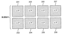
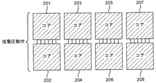
図15Aは本実施形態に係るアプリケーションであって、すべてのコア201〜208を高速動作で動作させたときのブロック図であり、図15Bは本実施形態に係るアプリケーションであって、各コア対(201,202)(203,204)(205,206)(207,208)で接続して低電圧動作させたときのブロック図である。図15A及び図15Bから明らかなように、応用するアプリケーションに応じて、演算負荷が比較的高い場合はすべてのコア201〜208を高速動作させるが、演算負荷が比較的低い場合は各コア対(201,202)(203,204)(205,206)(207,208)で接続して低電圧動作させることができる。
15A is an application according to the present embodiment, and is a block diagram when all the
以上の実施形態に係るプロセッサ装置によれば、以下の特徴を有する。
(1)内部ノードを接続することで低電圧動作する。2つのフリップフロップ回路の内部ノードを接続することで低電圧動作できるようになる。
(2)複数の動作モードを有するフリップフロップ回路を提供する。低電圧では内部ノードを接続するが,標準電圧では内部ノード接続しないことで通常の数のフリップフロップ回路を使うことができる。
The processor device according to the above embodiment has the following features.
(1) Low voltage operation is performed by connecting internal nodes. By connecting the internal nodes of the two flip-flop circuits, a low voltage operation can be performed.
(2) A flip-flop circuit having a plurality of operation modes is provided. An internal node is connected at a low voltage, but a normal number of flip-flop circuits can be used by not connecting an internal node at a standard voltage.
最後に、以下の2つの問題点について考察する。 Finally, consider the following two problems.
(問題点1)2つのフリップフロップ回路のクロックの同期は大丈夫か。フリップフロップ回路の位置が離れているとスキューが問題にならないか。別のコアにある場合はさらに問題のように思う。
(回答1)クロック配線はクロックツリー合成では問題ないが、入力信号Dと入力信号/Dについてはスキューが生じる。この入力信号Dと入力信号/Dの配線によるスキューが問題とならないような低速動作時において、カップリングされたフリップフロップ回路は有効である。ここで、高速動作時には有効でないが、そもそもカップリングされたフリップフロップ回路は不要である。どうしても、入力信号Dと入力信号/Dのスキューが問題となる場合には、2つのフリップフロップ回路を離すことができないので、セルライブラリにカップリングされたフリップフロップ回路を用意しておき、フリップフロップ回路同士の物理的な距離を無くすように設計することもできる。
(Problem 1) Is the clock synchronization of the two flip-flop circuits all right? Is the skew a problem if the flip-flop circuit is located far away? I think it's even more problematic if it is in a different core.
(Answer 1) Although there is no problem with the clock wiring in the clock tree synthesis, the input signal D and the input signal / D are skewed. The coupled flip-flop circuit is effective in a low-speed operation in which the skew due to the wiring of the input signal D and the input signal / D does not become a problem. Here, although not effective during high-speed operation, a coupled flip-flop circuit is not necessary in the first place. If the skew between the input signal D and the input signal / D is a problem, the two flip-flop circuits cannot be separated. Therefore, a flip-flop circuit coupled to the cell library is prepared, It can also be designed to eliminate the physical distance between circuits.
(問題点2)プロセスやセルライブラリ依存性は無いか。もしpMOSトランジスタ側が強いプロセスやライブラリだと別の現象になり、その場合でも有効かどうか心配である。一般性について確信が持てない。
(回答2)ラッチ回路の保持特性はnMOSトランジスタとpMOSトランジスタのしきい値の乖離が主因である。正確に双方のバランスが取れていれば原理的に超低電圧動作が可能となるが、事実上プロセスバラつきは避けられない。また移動度も大きく異なる。しきい値の不一致が生じれば、例えばpMOSトランジスタが強い状況でも指摘している保持特性の悪化が生じるので、本実施形態に係る回路は有効である。
(Problem 2) Is there dependency on the process or cell library? If the pMOS transistor side is a strong process or library, it will be a different phenomenon. I'm not sure about generality.
(Answer 2) The retention characteristic of the latch circuit is mainly due to the difference between the threshold values of the nMOS transistor and the pMOS transistor. In principle, ultra-low voltage operation is possible if both are accurately balanced, but process variations are inevitable in practice. The mobility is also greatly different. If the mismatch of the threshold value occurs, for example, the retention characteristic that has been pointed out deteriorates even when the pMOS transistor is strong. Therefore, the circuit according to this embodiment is effective.
以上説明したように、本実施形態によれば、電圧スケーリングモード及び速度ブースティングモードのためのプロセッサ装置のカップリングを提案した。ここで、7T/14TカップリングSRAMは、2個のビットセルを接続することにより、低電圧動作と高電圧動作の両方を実行することができる。カップリングされたフリップフロップ回路FF1,FF2は0.3V以下の動作電圧で動作することができ、これにより、動作電圧領域を従来技術に比較して大幅に広げることができる。また、カップリングされた論理回路は好ましいデータパスを選択することでプロセスバラツキに応じて選択的に採用可能である。 As described above, according to the present embodiment, the coupling of the processor device for the voltage scaling mode and the speed boosting mode is proposed. Here, the 7T / 14T coupling SRAM can execute both a low voltage operation and a high voltage operation by connecting two bit cells. The coupled flip-flop circuits FF1 and FF2 can operate at an operating voltage of 0.3 V or less, and thus the operating voltage range can be greatly expanded as compared with the prior art. Further, the coupled logic circuit can be selectively employed according to process variations by selecting a preferable data path.
以上詳述したように、本発明によれば、所定の第1の動作電圧で動作させる第1の電圧モード時に、上記第3乃至第6のゲートを開放することにより上記第1のフリップフロップ回路と上記第2のフリップフロップ回路とを別々に動作させる一方、上記第1の動作電圧よりも低い第2の動作電圧で動作させる第2の電圧モード時に、上記第3乃至第6のゲートを短絡することにより上記第1のフリップフロップ回路と上記第2のフリップフロップ回路とを互いに反転関係のデータを保持して相補的なデータ処理を行うように協働動作させる。すなわち、2種類の動作モードを有し、例えば所定の標準電圧では一般的なフリップフロップ回路と同様に動作する一方、例えば低電圧モードでは、2つのフリップフロップ回路の内部ノードを接続し、フリップフロップ回路装置の容量は半分になるが低電圧で動作することができる。ここで、低電圧モードでは、分離されたフリップフロップ回路の各ラッチ回路においてデータの保持力を小さいが、内部ノードを接続することで相補的にデータの保持力を増大させて動作させることができる。 As described above in detail, according to the present invention, the first flip-flop circuit is opened by opening the third to sixth gates in the first voltage mode for operating at a predetermined first operating voltage. And the second flip-flop circuit are operated separately, while the third to sixth gates are short-circuited in the second voltage mode in which the second flip-flop circuit is operated at a second operating voltage lower than the first operating voltage. Thus, the first flip-flop circuit and the second flip-flop circuit are cooperatively operated so as to hold complementary data and perform complementary data processing. That is, it has two types of operation modes, for example, operates in the same manner as a general flip-flop circuit at a predetermined standard voltage, while, for example, in the low-voltage mode, the internal nodes of the two flip-flop circuits are connected to each other. Although the capacity of the circuit device is halved, it can operate at a low voltage. Here, in the low voltage mode, the data holding power is small in each latch circuit of the separated flip-flop circuit, but it can be operated by complementaryly increasing the data holding power by connecting the internal nodes. .
1…プロセッサIC、
10…プロセッサコア(コア)、
11…ポジティブ・トゥルーのプロセッサエレメント(pPE)、
12…ネガティブ・トゥルーのプロセッサエレメント(nPE)、
13…フリップフロップ回路部、
13a,13b…フリップフロップ回路、
14…論理回路部、
14a,14b…論理回路、
15…SRAM、
15a,15b…1/2SRAM、
16…インバータ、
21〜24,31〜34,40〜48,40a,51〜58,60,61,62,70,71,72,100…インバータ、
30…CK信号発生部、
35…フリップフロップ回路部(FF回路部)、
36…入力信号回路部、
37…ゲート回路部、
100A…インバータゲート回路、
201〜208…コア、
FF1〜FF32…フリップフロップ回路、
L1〜L82…ラッチ回路、
LN1,LN2…ライン、
N21〜N34…内部ノード、
NAND1〜NAND22…ナンドゲート、
NOR1〜NOR3…ノアゲート、
Q1〜Q126…MOSトランジスタ、
T1,T2…端子、
TG1〜TG33…伝送ゲート、
TR100…転送ゲート。
1 ... Processor IC,
10: Processor core (core),
11 ... Positive True processor element (pPE),
12 ... Negative true processor element (nPE),
13 ... flip-flop circuit section,
13a, 13b ... flip-flop circuits,
14 ... logic circuit part,
14a, 14b ... logic circuits,
15 ... SRAM,
15a, 15b ... 1/2 SRAM,
16 ... an inverter,
21-24, 31-34, 40-48, 40a, 51-58, 60, 61, 62, 70, 71, 72, 100 ... inverter,
30 ... CK signal generator,
35 ... flip-flop circuit part (FF circuit part),
36: Input signal circuit section,
37. Gate circuit section,
100A ... inverter gate circuit,
201-208 ... core,
FF1 to FF32 ... flip-flop circuit,
L1 to L82 ... latch circuit,
LN1, LN2 ... line,
N21 to N34 ... internal nodes,
NAND1 to NAND22 ... NAND gate,
NOR1 to NOR3: NOR gate,
Q1-Q126 ... MOS transistors,
T1, T2 ... terminals,
TG1 to TG33 ... transmission gate,
TR100: Transfer gate.
Claims (7)
それぞれ入力側端子及び出力側端子を有する第3のラッチ回路と第4のラッチ回路とを第2のゲートを介して接続して構成された第2のフリップフロップ回路と、
上記第1のラッチ回路の入力側端子と、上記第3のラッチ回路の出力側端子との間を短絡又は開放し、短絡時に同一の論理値を有する第3のゲートと、
上記第1のラッチ回路の出力側端子と、上記第3のラッチ回路の入力側端子との間を短絡又は開放し、短絡時に同一の論理値を有する第4のゲートと、
上記第2のラッチ回路の入力側端子と、上記第4のラッチ回路の出力側端子との間を短絡又は開放し、短絡時に同一の論理値を有する第5のゲートと、
上記第2のラッチ回路の出力側端子と、上記第4のラッチ回路の入力側端子との間を短絡又は開放し、短絡時に同一の論理値を有する第6のゲートとを備えたフリップフロップ回路装置であって、
所定の第1の動作電圧で動作させる第1の電圧モード時に、上記第3乃至第6のゲートを開放することにより上記第1のフリップフロップ回路と上記第2のフリップフロップ回路とを別々に動作させる一方、上記第1の動作電圧よりも低い第2の動作電圧で動作させる第2の電圧モード時に、上記第3乃至第6のゲートを短絡することにより上記第1のフリップフロップ回路と上記第2のフリップフロップ回路とを互いに反転関係のデータを保持して相補的なデータ処理を行うように協働動作させることを特徴とするフリップフロップ回路装置。 A first flip-flop circuit configured by connecting a first latch circuit and an second latch circuit each having an input-side terminal and an output-side terminal via a first gate;
A second flip-flop circuit configured by connecting a third latch circuit and an fourth latch circuit each having an input side terminal and an output side terminal via a second gate;
A third gate that short-circuits or opens between the input-side terminal of the first latch circuit and the output-side terminal of the third latch circuit, and has the same logical value when short-circuited;
A fourth gate that short-circuits or opens between the output-side terminal of the first latch circuit and the input-side terminal of the third latch circuit, and has the same logical value when short-circuited;
A fifth gate that short-circuits or opens between the input-side terminal of the second latch circuit and the output-side terminal of the fourth latch circuit, and has the same logical value when short-circuited;
A flip-flop circuit comprising a sixth gate that short-circuits or opens between the output-side terminal of the second latch circuit and the input-side terminal of the fourth latch circuit and has the same logical value when short-circuited A device,
The first flip-flop circuit and the second flip-flop circuit are operated separately by opening the third to sixth gates in the first voltage mode for operating at a predetermined first operating voltage. On the other hand, the second flip-flop circuit and the first flip-flop circuit are short-circuited by short-circuiting the third to sixth gates in the second voltage mode in which the second operating voltage is lower than the first operating voltage. A flip-flop circuit device, wherein two flip-flop circuits are operated in a cooperative manner so as to hold complementary data and perform complementary data processing.
上記第2のフリップフロップ回路は、上記第3のラッチ回路に記憶されたデータを上記転送期間において上記第2のゲートを介して上記第4のラッチ回路に転送して出力することにより、上記第1のフリップフロップ回路とは互いに反転関係のデータを保持し、
上記第3のゲートは、上記第1のラッチ回路の入力側端子と、上記第3のラッチ回路の出力側端子との間に接続されかつ上記第1のラッチ回路の入力側端子と上記第3のラッチ回路の出力側端子との間を短絡又は開放し、上記短絡時に上記第1のラッチ回路の入力側端子及び上記第3のラッチ回路の出力側端子において同一の論理値を有し、
上記第4のゲートは、上記第1のラッチ回路の出力側端子と、上記第3のラッチ回路の入力側端子との間に接続されかつ上記第1のラッチ回路の出力側端子と上記第3のラッチ回路の入力側端子との間を短絡又は開放し、上記短絡時に上記第1のラッチ回路の出力側端子及び上記第3のラッチ回路の入力側端子において同一の論理値を有し、
上記第5のゲートは、上記第2のラッチ回路の入力側端子と、上記第4のラッチ回路の出力側端子との間に接続されかつ上記第2のラッチ回路の入力側端子と上記第4のラッチ回路の出力側端子との間を短絡又は開放し、上記短絡時に上記第2のラッチ回路の入力側端子及び上記第4のラッチ回路の出力側端子において同一の論理値を有し、
上記第6のゲートは、上記第2のラッチ回路の出力側端子と、上記第4のラッチ回路の入力側端子との間に接続されかつ上記第2のラッチ回路の出力側端子と上記第4のラッチ回路の入力側端子との間を短絡又は開放し、上記短絡時に上記第2のラッチ回路の出力側端子及び上記第4のラッチ回路の入力側端子において同一の論理値を有することを特徴とする請求項1記載のフリップフロップ回路装置。 The first flip-flop circuit transfers the data stored in the first latch circuit to the second latch circuit through the first gate and outputs the data in a predetermined transfer period,
The second flip-flop circuit transfers the data stored in the third latch circuit to the fourth latch circuit via the second gate and outputs the data in the transfer period, whereby the second flip-flop circuit outputs the data. 1 flip-flop circuit holds data in an inversion relationship with each other,
The third gate is connected between the input-side terminal of the first latch circuit and the output-side terminal of the third latch circuit, and the input-side terminal of the first latch circuit and the third gate Between the output side terminal of the first latch circuit and the output side terminal of the third latch circuit at the time of the short circuit,
The fourth gate is connected between the output-side terminal of the first latch circuit and the input-side terminal of the third latch circuit, and the output-side terminal of the first latch circuit and the third gate Between the input side terminals of the first latch circuit and the input side terminals of the third latch circuit at the time of the short circuit, and having the same logical value,
The fifth gate is connected between the input side terminal of the second latch circuit and the output side terminal of the fourth latch circuit, and the input side terminal of the second latch circuit and the fourth gate. Between the output side terminal of the second latch circuit and the output side terminal of the fourth latch circuit at the time of the short circuit,
The sixth gate is connected between the output side terminal of the second latch circuit and the input side terminal of the fourth latch circuit, and the output side terminal of the second latch circuit and the fourth gate. And the output side terminal of the second latch circuit and the input side terminal of the fourth latch circuit have the same logical value at the time of the short circuit. The flip-flop circuit device according to claim 1.
上記第2のラッチ回路はクロスカップリングされた第3及び第4のインバータを含み、
上記第3のラッチ回路はクロスカップリングされた第5及び第6のインバータを含み、
上記第4のラッチ回路はクロスカップリングされた第7及び第8のインバータを含み、
上記第2の電圧モード時に、上記第6のインバータからの出力信号を上記第1のインバータからの出力信号により同一の論理値で補強して上記第1のラッチ回路の出力側端子からの出力信号の信号保持力を増大させ、上記第2のインバータからの出力信号を上記第5のインバータからの出力信号により同一の論理値で補強して上記第3のラッチ回路の出力側端子からの出力信号の信号保持力を増大させ、
上記第2の電圧モード時に、上記第8のインバータからの出力信号を上記第3のインバータからの出力信号により同一の論理値で補強して上記第2のラッチ回路の出力側端子からの出力信号の信号保持力を増大させ、上記第4のインバータからの出力信号を上記第7のインバータからの出力信号により同一の論理値で補強して上記第4のラッチ回路の出力側端子からの出力信号の信号保持力を増大させることを特徴とする請求項2記載のフリップフロップ回路装置。 The first latch circuit includes first and second inverters that are cross-coupled;
The second latch circuit includes third and fourth inverters that are cross-coupled,
The third latch circuit includes fifth and sixth inverters that are cross-coupled,
The fourth latch circuit includes seventh and eighth inverters that are cross-coupled,
In the second voltage mode, the output signal from the sixth inverter is reinforced with the same logical value by the output signal from the first inverter, and the output signal from the output side terminal of the first latch circuit Output signal from the output terminal of the third latch circuit by reinforcing the output signal from the second inverter with the same logic value by the output signal from the fifth inverter. Increase the signal holding power of
In the second voltage mode, the output signal from the eighth inverter is reinforced with the same logical value by the output signal from the third inverter, and the output signal from the output side terminal of the second latch circuit And the output signal from the fourth inverter is reinforced with the same logical value by the output signal from the seventh inverter, and the output signal from the output side terminal of the fourth latch circuit. 3. The flip-flop circuit device according to claim 2, wherein the signal holding power of the flip-flop circuit is increased.
上記第5のインバータの出力電力を上記第2のインバータの出力電力よりも大きくなるように設定し、
上記第3のインバータの出力電力を上記第8のインバータの出力電力よりも大きくなるように設定し、
上記第7のインバータの出力電力を上記第4のインバータの出力電力よりも大きくなるように設定したことを特徴とする請求項3記載のフリップフロップ回路装置。 Setting the output power of the first inverter to be larger than the output power of the sixth inverter;
Setting the output power of the fifth inverter to be larger than the output power of the second inverter;
The output power of the third inverter is set to be larger than the output power of the eighth inverter,
4. The flip-flop circuit device according to claim 3, wherein the output power of the seventh inverter is set to be larger than the output power of the fourth inverter.
Priority Applications (1)
| Application Number | Priority Date | Filing Date | Title |
|---|---|---|---|
| JP2011125500A JP5284415B2 (en) | 2011-06-03 | 2011-06-03 | Flip-flop circuit device and processor device using the same |
Applications Claiming Priority (1)
| Application Number | Priority Date | Filing Date | Title |
|---|---|---|---|
| JP2011125500A JP5284415B2 (en) | 2011-06-03 | 2011-06-03 | Flip-flop circuit device and processor device using the same |
Publications (2)
| Publication Number | Publication Date |
|---|---|
| JP2012253612A JP2012253612A (en) | 2012-12-20 |
| JP5284415B2 true JP5284415B2 (en) | 2013-09-11 |
Family
ID=47526000
Family Applications (1)
| Application Number | Title | Priority Date | Filing Date |
|---|---|---|---|
| JP2011125500A Expired - Fee Related JP5284415B2 (en) | 2011-06-03 | 2011-06-03 | Flip-flop circuit device and processor device using the same |
Country Status (1)
| Country | Link |
|---|---|
| JP (1) | JP5284415B2 (en) |
Families Citing this family (1)
| Publication number | Priority date | Publication date | Assignee | Title |
|---|---|---|---|---|
| US11791819B2 (en) * | 2019-12-26 | 2023-10-17 | Intel Corporation | Low power flip-flop with reduced parasitic capacitance |
Family Cites Families (3)
| Publication number | Priority date | Publication date | Assignee | Title |
|---|---|---|---|---|
| JP4069963B2 (en) * | 1996-11-14 | 2008-04-02 | 富士通株式会社 | MOS transistor threshold compensation circuit and flip-flop type sense amplifier having the same |
| JP2008131320A (en) * | 2006-11-21 | 2008-06-05 | Sony Corp | Flip-flop circuit and display device |
| JP2008219491A (en) * | 2007-03-05 | 2008-09-18 | Nec Electronics Corp | Master slave type flip-flop circuit and latch circuit |
-
2011
- 2011-06-03 JP JP2011125500A patent/JP5284415B2/en not_active Expired - Fee Related
Also Published As
| Publication number | Publication date |
|---|---|
| JP2012253612A (en) | 2012-12-20 |
Similar Documents
| Publication | Publication Date | Title |
|---|---|---|
| KR100418233B1 (en) | Semiconductor storage device | |
| KR101564340B1 (en) | Low-power 5t sram with improved stability and reduced bitcell size | |
| US6232810B1 (en) | Flip-flop | |
| WO2015172412A1 (en) | Improved sram storage unit based on dice structure | |
| KR100192068B1 (en) | Semiconductor integrated circuit device | |
| US20090039936A1 (en) | Flip-flop circuit, pipeline circuit including a flip-flop circuit, and method of operating a flip-flop circuit | |
| US9384825B2 (en) | Multi-port memory circuits | |
| JPS60127598A (en) | Semiconductor integrated circuit device | |
| JP5284415B2 (en) | Flip-flop circuit device and processor device using the same | |
| CN109119112B (en) | Storage unit circuit for improving read-write stability and storage device | |
| JPH01158693A (en) | Data output buffer of static ram using high impedance | |
| JP2771375B2 (en) | Level shift circuit | |
| US8736304B2 (en) | Self-biased high speed level shifter circuit | |
| US6509772B1 (en) | Flip-flop circuit with transmission-gate sampling | |
| JP3533357B2 (en) | Semiconductor integrated circuit with logical operation function | |
| JP3513158B2 (en) | Semiconductor integrated circuit device | |
| KR100331520B1 (en) | Write multiplexer apparatus and method for multiple write port programmable memory | |
| US20040062089A1 (en) | Memory device | |
| KR20050067528A (en) | Driving circuit for on die termination in semiconductor and its method | |
| KR100348306B1 (en) | Level shifter | |
| JP4566602B2 (en) | Development method of semiconductor integrated circuit | |
| JPS6037822A (en) | Cmos logical circuit | |
| US7285986B2 (en) | High speed, low power CMOS logic gate | |
| JP3698929B2 (en) | Semiconductor memory device | |
| KR20010083242A (en) | Semiconductor integrated circuit device |
Legal Events
| Date | Code | Title | Description |
|---|---|---|---|
| A977 | Report on retrieval |
Free format text: JAPANESE INTERMEDIATE CODE: A971007 Effective date: 20130513 |
|
| A01 | Written decision to grant a patent or to grant a registration (utility model) |
Free format text: JAPANESE INTERMEDIATE CODE: A01 Effective date: 20130521 |
|
| A61 | First payment of annual fees (during grant procedure) |
Free format text: JAPANESE INTERMEDIATE CODE: A61 Effective date: 20130529 |
|
| LAPS | Cancellation because of no payment of annual fees |