JP5284401B2 - Operation switching device and program - Google Patents
Operation switching device and program Download PDFInfo
- Publication number
- JP5284401B2 JP5284401B2 JP2011065704A JP2011065704A JP5284401B2 JP 5284401 B2 JP5284401 B2 JP 5284401B2 JP 2011065704 A JP2011065704 A JP 2011065704A JP 2011065704 A JP2011065704 A JP 2011065704A JP 5284401 B2 JP5284401 B2 JP 5284401B2
- Authority
- JP
- Japan
- Prior art keywords
- interrupt
- unit
- processor
- time
- waiting time
- Prior art date
- Legal status (The legal status is an assumption and is not a legal conclusion. Google has not performed a legal analysis and makes no representation as to the accuracy of the status listed.)
- Expired - Fee Related
Links
Images


Classifications
-
- G—PHYSICS
- G06—COMPUTING OR CALCULATING; COUNTING
- G06F—ELECTRIC DIGITAL DATA PROCESSING
- G06F9/00—Arrangements for program control, e.g. control units
- G06F9/06—Arrangements for program control, e.g. control units using stored programs, i.e. using an internal store of processing equipment to receive or retain programs
- G06F9/46—Multiprogramming arrangements
- G06F9/48—Program initiating; Program switching, e.g. by interrupt
- G06F9/4806—Task transfer initiation or dispatching
- G06F9/4843—Task transfer initiation or dispatching by program, e.g. task dispatcher, supervisor, operating system
- G06F9/4881—Scheduling strategies for dispatcher, e.g. round robin, multi-level priority queues
- G06F9/4893—Scheduling strategies for dispatcher, e.g. round robin, multi-level priority queues taking into account power or heat criteria
-
- G—PHYSICS
- G06—COMPUTING OR CALCULATING; COUNTING
- G06F—ELECTRIC DIGITAL DATA PROCESSING
- G06F1/00—Details not covered by groups G06F3/00 - G06F13/00 and G06F21/00
- G06F1/26—Power supply means, e.g. regulation thereof
- G06F1/32—Means for saving power
- G06F1/3203—Power management, i.e. event-based initiation of a power-saving mode
- G06F1/3206—Monitoring of events, devices or parameters that trigger a change in power modality
- G06F1/3228—Monitoring task completion, e.g. by use of idle timers, stop commands or wait commands
-
- G—PHYSICS
- G06—COMPUTING OR CALCULATING; COUNTING
- G06F—ELECTRIC DIGITAL DATA PROCESSING
- G06F1/00—Details not covered by groups G06F3/00 - G06F13/00 and G06F21/00
- G06F1/26—Power supply means, e.g. regulation thereof
- G06F1/32—Means for saving power
- G06F1/3203—Power management, i.e. event-based initiation of a power-saving mode
- G06F1/3234—Power saving characterised by the action undertaken
- G06F1/324—Power saving characterised by the action undertaken by lowering clock frequency
-
- G—PHYSICS
- G06—COMPUTING OR CALCULATING; COUNTING
- G06F—ELECTRIC DIGITAL DATA PROCESSING
- G06F1/00—Details not covered by groups G06F3/00 - G06F13/00 and G06F21/00
- G06F1/26—Power supply means, e.g. regulation thereof
- G06F1/32—Means for saving power
- G06F1/3203—Power management, i.e. event-based initiation of a power-saving mode
- G06F1/3234—Power saving characterised by the action undertaken
- G06F1/3243—Power saving in microcontroller unit
-
- G—PHYSICS
- G06—COMPUTING OR CALCULATING; COUNTING
- G06F—ELECTRIC DIGITAL DATA PROCESSING
- G06F1/00—Details not covered by groups G06F3/00 - G06F13/00 and G06F21/00
- G06F1/26—Power supply means, e.g. regulation thereof
- G06F1/32—Means for saving power
- G06F1/3203—Power management, i.e. event-based initiation of a power-saving mode
- G06F1/3234—Power saving characterised by the action undertaken
- G06F1/3287—Power saving characterised by the action undertaken by switching off individual functional units in the computer system
-
- Y—GENERAL TAGGING OF NEW TECHNOLOGICAL DEVELOPMENTS; GENERAL TAGGING OF CROSS-SECTIONAL TECHNOLOGIES SPANNING OVER SEVERAL SECTIONS OF THE IPC; TECHNICAL SUBJECTS COVERED BY FORMER USPC CROSS-REFERENCE ART COLLECTIONS [XRACs] AND DIGESTS
- Y02—TECHNOLOGIES OR APPLICATIONS FOR MITIGATION OR ADAPTATION AGAINST CLIMATE CHANGE
- Y02D—CLIMATE CHANGE MITIGATION TECHNOLOGIES IN INFORMATION AND COMMUNICATION TECHNOLOGIES [ICT], I.E. INFORMATION AND COMMUNICATION TECHNOLOGIES AIMING AT THE REDUCTION OF THEIR OWN ENERGY USE
- Y02D10/00—Energy efficient computing, e.g. low power processors, power management or thermal management
-
- Y—GENERAL TAGGING OF NEW TECHNOLOGICAL DEVELOPMENTS; GENERAL TAGGING OF CROSS-SECTIONAL TECHNOLOGIES SPANNING OVER SEVERAL SECTIONS OF THE IPC; TECHNICAL SUBJECTS COVERED BY FORMER USPC CROSS-REFERENCE ART COLLECTIONS [XRACs] AND DIGESTS
- Y02—TECHNOLOGIES OR APPLICATIONS FOR MITIGATION OR ADAPTATION AGAINST CLIMATE CHANGE
- Y02D—CLIMATE CHANGE MITIGATION TECHNOLOGIES IN INFORMATION AND COMMUNICATION TECHNOLOGIES [ICT], I.E. INFORMATION AND COMMUNICATION TECHNOLOGIES AIMING AT THE REDUCTION OF THEIR OWN ENERGY USE
- Y02D30/00—Reducing energy consumption in communication networks
- Y02D30/50—Reducing energy consumption in communication networks in wire-line communication networks, e.g. low power modes or reduced link rate
Landscapes
- Engineering & Computer Science (AREA)
- Theoretical Computer Science (AREA)
- General Engineering & Computer Science (AREA)
- Physics & Mathematics (AREA)
- General Physics & Mathematics (AREA)
- Software Systems (AREA)
- Computer Hardware Design (AREA)
- Computing Systems (AREA)
- Power Sources (AREA)
Abstract
Description
本発明の実施形態は、動作切替装置およびプログラムに関する。 Embodiments described herein relate generally to an operation switching device and a program.
従来、1または複数の処理を実行可能な処理装置(例えばマイクロプロセッサ)の消費電力を低減する技術が知られている。例えば、電源電圧や周波数を下げて消費電力を低減するDVFS(Dynamic Voltage Frequency Scalling)と呼ばれる技術や、電力を必要としている部分にだけ電力を供給するパワーゲーティング技術などが挙げられる。 Conventionally, a technique for reducing power consumption of a processing apparatus (for example, a microprocessor) capable of executing one or a plurality of processes is known. For example, there is a technique called DVFS (Dynamic Voltage Frequency Scalling) that reduces power consumption by lowering a power supply voltage or frequency, and a power gating technique that supplies power only to a portion that requires power.
パワーゲーティング技術の例として、プロセッサ内を複数のクロックドメインに分割し、各クロックドメイン内で電力を供給するか否かを決定する技術がある。また、プロセッサ内の演算器単位で電力を供給するか否かを決定する細粒度パワーゲーティング技術がある。 As an example of the power gating technique, there is a technique for dividing a processor into a plurality of clock domains and determining whether or not to supply power in each clock domain. There is also a fine-grain power gating technique that determines whether or not to supply power in units of arithmetic units in a processor.
また、マイクロプロセッサの消費電力を低減する別の手法として、プロセッサ全体を一時的に停止させて節電状態(スリープ状態)にする技術がある。 As another technique for reducing the power consumption of the microprocessor, there is a technique for temporarily stopping the entire processor to enter a power saving state (sleep state).
しかしながら、従来の技術では、マイクロプロセッサなどの処理装置の消費電力を効率的に低減することは困難であるという問題がある。本発明が解決しようとする課題は、処理装置の消費電力を効率的に低減可能な動作切替装置およびプログラムを提供することである。 However, the conventional technology has a problem that it is difficult to efficiently reduce the power consumption of a processing device such as a microprocessor. The problem to be solved by the present invention is to provide an operation switching device and a program capable of efficiently reducing the power consumption of the processing device.
実施形態の動作切替装置は、1または複数の処理を実行可能な処理装置が前記処理を実行していないアイドル状態を検出する状態検出部と、割り込み処理の種別を示す割り込み種別と、当該割り込み種別の割り込み待ちが発生した時刻とを記憶する第4記憶部と、前記割り込み種別と、当該割り込み種別に対応する割り込み待ち時間とを記憶する第5記憶部と、前記状態検出部で前記アイドル状態が検出されたとき、前記第4記憶部に記憶された情報と、前記第5記憶部に記憶された情報に基づいて、現在時刻から、次の前記割り込み処理が開始されるまでの時間長を示す待ち時間を算出する算出部と、前記算出部で算出された前記待ち時間に応じて、前記処理装置の動作モードを決定する決定部と、を備えることを特徴とする。 The operation switching device according to the embodiment includes a state detection unit that detects an idle state in which a processing device capable of executing one or a plurality of processes is not executing the processing , an interrupt type indicating a type of interrupt processing, and the interrupt type A fourth storage unit that stores a time at which an interrupt wait occurs, a fifth storage unit that stores the interrupt type and an interrupt wait time corresponding to the interrupt type, and the idle state is detected by the state detection unit. When detected, based on the information stored in the fourth storage unit and the information stored in the fifth storage unit, the time length from the current time until the next interrupt processing is started is indicated. A calculation unit that calculates a waiting time; and a determination unit that determines an operation mode of the processing device according to the waiting time calculated by the calculation unit.
また、実施形態のプログラムは、1または複数の処理を実行可能な処理装置が前記処理を実行していないアイドル状態を検出する手順と、前記アイドル状態検出部で前記アイドル状態が検出されたとき、割り込み処理の種別を示す割り込み種別と、当該割り込み種別の割り込み待ちが発生した時刻とを記憶する第4記憶部に記憶された情報と、前記割り込み種別と、当該割り込み種別に対応する割り込み待ち時間とを記憶する第5記憶部に記憶された情報に基づいて、次の前記割り込み処理が開始されるまでの時間長を示す待ち時間を算出する手順と、前記算出部で算出された前記待ち時間に応じて、前記処理装置の動作モードを決定する手順と、をコンピュータに実行させるためのプログラムである。 Further, the program of the embodiment includes a procedure for detecting an idle state in which a processing apparatus capable of executing one or a plurality of processes is not executing the process, and when the idle state is detected by the idle state detection unit, Information stored in a fourth storage unit that stores an interrupt type indicating the type of interrupt processing, and a time when an interrupt wait of the interrupt type occurs, the interrupt type, and an interrupt wait time corresponding to the interrupt type On the basis of the information stored in the fifth storage unit for storing the waiting time indicating the time length until the next interrupt processing is started, and the waiting time calculated by the calculating unit Accordingly, a program for causing a computer to execute a procedure for determining an operation mode of the processing device.
(第1実施形態)
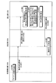
図1は、本実施形態のターゲットシステムの概略構成の一例を示すブロック図である。図1に示すように、ターゲットシステムは、プロセッサ100と、再開制御部700と、記憶領域900と、を備え、それぞれがバス950で相互に接続されている。プロセッサ100は、1または複数の処理を実行可能な処理装置である。図1に示すように、プロセッサ100は、CPU20と第3記憶部110とを有する。より具体的には、第3記憶部110は、各種のデータが記憶されるレジスタ120と、使用頻度の高いデータなどが記憶されるキャッシュメモリ140とを含む。本実施形態では、レジスタ120およびキャッシュメモリ140の各々は揮発性のメモリで構成される。
(First embodiment)
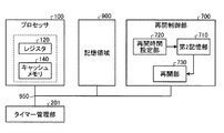
FIG. 1 is a block diagram illustrating an example of a schematic configuration of a target system according to the present embodiment. As shown in FIG. 1, the target system includes a
再開制御部700は、後述の節電状態(スリープ状態)にされたプロセッサ100の動作を再開させるための手段である。図1に示すように、再開制御部700は、第2記憶部710と、再開時間設定部720と、再開部730とを有する。第2記憶部710は、後述の待ち時間を記憶する。再開時間設定部720は、プロセッサ100から通知された待ち時間を第2記憶部710に設定する。再開部730は、第2記憶部710に記憶された待ち時間に到達したことを検出すると、プロセッサ100の動作を再開させる。これらの詳細な動作については後述する。
The
記憶領域900は、電源Offした後で再度電源ONした場合に、その内部データを復元できる。これを実現する記憶領域として、例えば不揮発性メモリと呼ばれるものがあり、MRAM(Magnetic Random Access Memory)やFeRAM(Ferroelectric Random Access Memory)で構成することができる。また、不揮発性メモリに限らず、通常のDRAM(Dynamic Random Access Memory)であっても電源ON時に内部データを復元させる機構を持つものもこれに該当する。
The
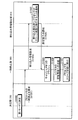
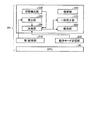
図2は、プロセッサ100に搭載されたCPU20が、基本ソフトウェアであるOS(operating system)200を実行することにより実現される機能の構成と、プロセッサ100が備えるハードウェアとを示すブロック図である。ここでは、プロセッサ100上で単一のOS200が動作し、OS200上で1または複数のプロセス(500−1〜500−n)が動作すると捉えることができる。また、図2においては、プロセッサ100が備えるハードウェアとプロセッサ100上で動作するOS200、OS200上で動作する1または複数のプロセスをプロセッサ100が含む表現としている。
FIG. 2 is a block diagram illustrating a configuration of functions realized by the
図2に示すように、プロセッサ100が備えるハードウェアには、CPU20と、第1記憶部210と、動作モード記憶部220とが含まれる。第1記憶部210は、タイマー情報を記憶する。タイマー情報には、設定時刻と、当該設定時刻に実行する処理とが含まれる。動作モード記憶部220は、後述の待ち時間と、設定すべき動作モードとの関係を記憶する。この詳細な内容については後述する。
As illustrated in FIG. 2, the hardware included in the
図2に示すように、OS200は、状態検出部230と、算出部240と、決定部250と、維持部260と、一時停止部270と、復帰部280とを有する。状態検出部230は、アイドル状態を検出可能である。アイドル状態とは、プロセッサ100が何れの処理も実行していない状態を指す。
As illustrated in FIG. 2, the OS 200 includes a
算出部240は、状態検出部230によってアイドル状態が検出されたとき、第1記憶部210に記憶されたタイマー情報を用いて、次の処理が開始されるまでの時間長を示す待ち時間を求める。より具体的には、算出部240は、第1記憶部210に記憶されたタイマー情報から、次の処理が開始される時刻を求め、その求めた時刻と現在時刻との差分の時間長を、待ち時間として求める。
When the idle state is detected by the
決定部250は、算出部240から上述の待ち時間を取得し、その取得した待ち時間に応じて、プロセッサ100の動作モードを決定する。より具体的には、決定部250は、算出部240から取得した待ち時間と、動作モード記憶部220に記憶されたデータとから、プロセッサ100の動作モードを決定する。さらに詳述すると以下のとおりである。図3は、動作モード記憶部220に記憶される情報の一例を示す図である。図3に示すように、動作モード記憶部220は、待ち時間と、設定すべき動作モードとの関係を記憶する。決定部250は、待ち時間がt1を越える場合は、プロセッサ100の動作モードを、プロセッサの動作が一時的に停止して節電状態(スリープ状態)となる第1モードに決定する。一方、待ち時間がt1以下の場合は、決定部250は、プロセッサ100がアイドル状態を維持する第2モードに決定する。
The
維持部260は、プロセッサ100の動作モードが第2モードのときに、アイドル状態を維持するためのタスク(アイドルタスクと呼ぶ)を実行する。一時停止部270は、決定部250によって、プロセッサ100の動作モードが第1モードに決定されたときに、レジスタ120およびキャッシュメモリ140に記憶されたデータを記憶領域900に退避させ、プロセッサ100の動作を一時的に停止して節電状態(スリープ状態)にする。復帰部280は、スリープ状態にされていたプロセッサ100が動作を再開するときに、記憶領域900に退避されていたデータを、レジスタ120へ復帰させる。詳細な内容については後述する。
図4は、プロセッサ100のアイドル状態が検出されてから、プロセッサ100の動作モードが決定されるまでの手順の一例を示すシーケンス図である。図4に示すように、まず状態検出部230が、プロセッサ100のアイドル状態を検出し(S400)、決定部250に対して動作モードの決定を要求する(S401)。次に、決定部250は、算出部240に対して、待ち時間の算出を要求する(S402)。
FIG. 4 is a sequence diagram illustrating an example of a procedure from when the idle state of the
次に、算出部240は、第1記憶部210に記憶されたタイマー情報を読み出す(ステップS403)。次に、算出部240は、読み出したタイマー情報から、次の処理が実行される時刻を抽出し、その抽出した時刻と現在時刻との差分の時間長を待ち時間として算出する(S404)。そして、算出部240は、その算出した待ち時間を決定部250へ通知する(S405)。
Next, the
次に、決定部250は、算出部240から取得した待ち時間と、動作モード記憶部220に記憶されたデータとから、動作モードを決定する(S406)。
Next, the
図5は、プロセッサ100の動作モードが第1モードに決定されてから、プロセッサ100がスリープ状態にされるまでの手順の一例を示すシーケンス図である。図5に示すように、決定部250は、プロセッサ100の動作モードを第1モードに決定したとき(S500)、一時停止部270に対して、プロセッサ100の動作の一時停止を要求する(S501)。本実施形態では、決定部250は、プロセッサ100の一時停止の要求と併せて、算出部240から取得した待ち時間を、一時停止部270へ通知する。
FIG. 5 is a sequence diagram illustrating an example of a procedure from when the operation mode of the
次に、一時停止部270は、決定部250から通知された待ち時間を再開時間設定部720へ通知する(S502)。次に、再開時間設定部720は、一時停止部270から通知された待ち時間を第2記憶部710に登録する(S503)。次に、再開時間設定部720は、待ち時間の登録が完了したことを一時停止部270へ通知する(S504)。
Next, the
次に、一時停止部270は、キャッシュメモリ140に格納されたデータを記憶領域900へフラッシュする(S505)。フラッシュされた(送り出された)データは記憶領域900に書き込まれる。次に、一時停止部270は、レジスタ120に格納されたデータを記憶領域900へ退避する(S506)。次に、一時停止部270は、プロセッサ100の動作を一時的に停止して節電状態(スリープ状態)に移行させる(S507)。
Next, the
図6は、再開時間に到達してプロセッサ100の動作が再開されるまでの手順の一例を示すシーケンス図である。図6に示すように、再開部730は、再開時間に到達したことを検出したときに(S600)、プロセッサ100の動作を再開させて第1モードを解除する(S601)。
FIG. 6 is a sequence diagram illustrating an example of a procedure until the operation of the
次に、復帰部280は、一時停止部270によって記憶領域900に退避されていたデータを、レジスタ120へ復帰させる(スップS602)。そして、再開時間において実行すべき処理に移行する(S603)。
Next, the
以上に説明したように、本実施形態では、タイマー情報から求められた待ち時間に応じて、プロセッサ100の動作モードを決定する。より具体的には、待ち時間が所定の時間長(t1)を超える場合は、プロセッサ100をスリープ状態にする一方、待ち時間が所定の時間長以下の場合は、アイドル状態を維持するので、プロセッサ100の消費電力を効率的に低減できる。
As described above, in this embodiment, the operation mode of the
ここで、プロセッサ100をスリープ状態に移行させて消費電力を低減する方法は、プロセッサ100の消費電力を低減できる一方で、プロセッサ100を一時的に停止させるための処理等によるオーバーヘッドが大きいうえ、当該処理(例えばレジスタの退避および復帰やキャッシュメモリのフラッシュなどの処理)やそれによる影響(キャッシュメモリのフラッシュによるメモリアクセス増加等)で発生する消費電力も無視できない。このため、プロセッサ100がアイドル状態に移行してから、次の処理が実行されるまでの時間長(待ち時間)の値によっては、プロセッサ100をスリープ状態に移行させるときに発生する消費電力の方が、プロセッサ100をスリープ状態に移行させることによって低減できる消費電力よりも大きい場合がある。
Here, the method of reducing the power consumption by shifting the
本実施形態では、上述の待ち時間が所定の時間長を超えるときのみに、プロセッサ100をスリープ状態に移行させるので、効率的に消費電力を低減できるという利点がある。なお、本実施形態では、プロセッサ100のみを、プロセッサ100の動作モードを切り替え可能な動作切替装置として捉えることができるし、プロセッサ100と再開制御部700とを動作切替装置として捉えることもできる。
In the present embodiment, since the
(第2実施形態)
本実施形態では、プロセッサ100がアイドル状態になってから、最も早い割り込み処理が開始されるまでの時間長を待ち時間として算出する点で第1実施形態と異なる。以下、具体的な内容を説明する。なお、第1実施形態と共通する部分については、同一の符号を付して適宜に説明を省略する。
(Second Embodiment)
The present embodiment is different from the first embodiment in that a time length from when the
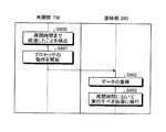
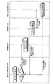
図7は、本実施形態のターゲットシステムの概略構成の一例を示すブロック図である。図7に示すように、ターゲットシステムは、プロセッサ100と、割り込み管理部800と、記憶領域900と、を備え、それぞれがバス950で相互に接続されている。割り込み管理部800は、プロセッサ100が節電状態(スリープ状態)になっている場合に、プロセッサ100の代わりに割り込みを管理する手段である。図7に示すように、割り込み管理部800は、割り込み管理設定部810と、割り込み検出部820と、再開部830とを有する。
FIG. 7 is a block diagram showing an example of a schematic configuration of the target system of the present embodiment. As shown in FIG. 7, the target system includes a
割り込み管理設定部810は、決定部250によってプロセッサ100の動作モードが第1モードに決定されたときに、割り込み検出部820に対して、プロセッサ100がスリープ状態に移行することを通知する。割り込み検出部820は、割り込み処理の発生を検出する。再開部830は、割り込み検出部820で割り込み処理の発生が検出されたときに、スリープ状態のプロセッサ100の動作を再開させる。割り込み検出部820は、割り込みを検出すると、プロセッサ100がスリープ状態のときには、再開部830に対して後述の再開要求を通知する。再開部830は、割り込み検出部820から再開要求が通知されたときに、スリープ状態のプロセッサ100の動作を再開させる。
When the
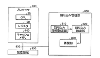
図8は、プロセッサ100に搭載されたCPU20が、OS300を実行することにより実現される機能の構成と、プロセッサ100が備えるハードウェアとを示すブロック図である。図8に示すように、プロセッサ100が備えるハードウェアには、CPU20と、第4記憶部310と、第5記憶部320と、動作モード記憶部220とが含まれる。また、図8においては、プロセッサ100が備えるハードウェアとプロセッサ100上で動作するOS300、OS300上で動作する1または複数のプロセスをプロセッサ100が含む表現としている。
FIG. 8 is a block diagram illustrating a configuration of functions realized by the
第4記憶部310は、割り込み待ち情報を記憶する。割り込み待ち情報には、割り込み処理の種別を示す割り込み種別と、当該割り込み種別の割り込み待ちが発生した時刻とが含まれる。図9は、第4記憶部310に記憶された割り込み待ち情報の一例を示す図である。図9の例では、割り込み種別は、デバイス読み出しとキーボード入力の2種類である。また、デバイス読み出しの割り込み待ちが発生した時刻はT_aであり、キーボード入力の割り込み待ちが発生した時刻はT_bである。
The
図8に示す第5記憶部320は、割り込み種別と、当該割り込み種別に対応する割り込み待ち時間とを記憶する。各割り込み種別に対応する割り込み待ち時間は、予め計算等によって求められた予測値である。図10は、第5記憶部320に記憶された情報の一例を示す図である。図10の例では、デバイス読み出しに対応する割り込み待ち時間はT3に設定される。また、キーボード入力に対応する割り込み待ち時間はT4に設定される。さらに、マウス入力に対応する割り込み待ち時間はT5に設定される。
The
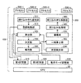
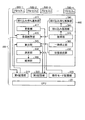
再び図8に戻って説明を続ける。図8に示すように、OS300は、割り込み待ち通知部311と、登録削除部313と、算出部325と、決定部250と、維持部260と、状態検出部230と、一時停止部365と、復帰部370と、割り込み処理部380と、割り込み待ち解除部390とを有する。割り込み待ち通知部311は、割り込み待ちが発生したときに、当該割り込み待ちとなった割り込み種別を、登録削除部313へ通知する。登録削除部313は、割り込み待ち通知部311から通知された割り込み種別と、当該割り込み種別の割り込み待ちが発生した時刻とを第4記憶部310に登録する。一方、登録削除部313は、割り込み処理が開始されるときに、割り込み待ちが解除された割り込み種別と、当該割り込み種別の割り込み待ちが発生した時刻とを第4記憶部310から削除する。詳細な内容については後述する。
Returning to FIG. 8 again, the description will be continued. As illustrated in FIG. 8, the
算出部325は、状態検出部230によってアイドル状態が検出されたとき、第4記憶部310に記憶された割り込み待ち情報と、第5記憶部320に記憶された情報とに基づいて、現在時刻から、次の割り込み処理が開始されるまでの時間長を待ち時間として算出する。詳細な内容については後述する。
When the idle state is detected by the
一時停止部365は、決定部250によって、プロセッサ100の動作モードが第1モードに決定されたときに、レジスタ120およびキャッシュメモリ140に記憶されたデータを記憶領域900に退避させ、プロセッサ100の動作を一時的に停止して節電状態(スリープ状態)にする。復帰部370は、スリープ状態にされていたプロセッサ100が動作を再開するときに、記憶領域900に退避されていたデータを、レジスタ120へ復帰させる。
When the
割り込み処理部380は、割り込み管理部800から、割り込み処理の発生を通知する割り込み通知を受信したときに、割り込み処理を開始する。また、割り込み処理部380は、割り込み管理部800からの割り込み通知を受信したときに、当該割り込み通知で特定される割り込み種別を、割り込み待ち解除部390へ通知する。割り込み待ち解除部390は、割り込み処理部380から通知された割り込み種別の割り込み待ちを解除する要求を、登録削除部313へ通知する。
When the interrupt
図11は、割り込み待ちが発生したときのプロセッサ100の動作手順の一例を示すシーケンス図である。本実施形態では、デバイスが割り込み待ちの状態になると、当該デバイスの割り込み待ちが発生したことを示す情報が、デバイスドライバ等から割り込み待ち通知部311へ通知される。図11に示すように、割り込み待ちが発生すると、割り込み待ち通知部311は、当該割り込み待ちとなった割り込み種別を登録削除部313へ通知する(ステップS1200)。登録削除部313は、割り込み待ち通知部311から通知された割り込み種別を受信したときに(S1201)、その受信した割り込み種別と、当該割り込み種別の割り込み待ちが発生した時刻とを第4記憶部310に登録する(S1202)。
FIG. 11 is a sequence diagram illustrating an example of an operation procedure of the
図12は、割り込み処理が発生したときのプロセッサ100の動作手順の一例を示すシーケンス図である。図12に示すように、割り込み処理部380は、割り込み管理部800からの割り込み通知を受信したときに(S1300)、当該割り込み通知で特定される割り込み種別を、割り込み待ち解除部390へ送信する(S1301)とともに、当該割り込み通知で特定される割り込み処理を開始する(S1304)。
FIG. 12 is a sequence diagram illustrating an example of an operation procedure of the
割り込み待ち解除部390は、割り込み処理部380から通知された割り込み種別の割り込み待ちを解除することを要求する割り込み待ち解除要求を、登録削除部313へ通知する(S1302)。登録削除部313は、割り込み待ち解除部390から割り込み待ちの解除を要求された割り込み種別と、当該割り込み種別の割り込み待ちが発生した時刻とを、第4記憶部310から削除する(S1303)。このように、第4記憶部310には、割り込み待ちが発生したときには、当該割り込み待ちとなった割り込み種別と、当該割り込み待ちが発生した時刻とが登録される一方、割り込み待ちが解除されたときには、割り込み待ちが解除される割り込み種別と、当該割り込み待ちが発生した時刻とが削除される。これにより、現在の割り込み待ちの状況を適切に管理することができる。
The interrupt
図13は、プロセッサ100のアイドル状態が検出されてから、プロセッサ100の動作モードが決定されるまでの手順の一例を示すシーケンス図である。図13に示すように、まず状態検出部230が、プロセッサ100のアイドル状態を検出し(ステップS1400)、決定部250に対して、動作モードの決定を要求する(S1401)。次に、決定部250は、算出部325に対して、次の割り込み処理が発生するまでの時間長を示す待ち時間の算出を要求する(S1402)。
FIG. 13 is a sequence diagram illustrating an example of a procedure from when the idle state of the
次に、算出部325は、第4記憶部310に記憶された割り込み待ち情報を取得する(S1403)。次に、算出部325は、現在割り込み待ちになっている割り込み種別に対応する割り込み待ち時間を第5記憶部320から取得する(S1404)。次に、算出部325は、第4記憶部310から取得した割り込み待ち情報と、第5記憶部320から取得した割り込み待ち時間とから、待ち時間を算出する(S1405)。
Next, the
ここで、算出部325による待ち時間の算出方法の具体例を説明する。例えば、現在、デバイス読み出しとキーボード入力の割り込み待ちであって、キーボード入力の割り込み待ちの発生時刻T_bの方が、デバイス読み出しの割り込み待ちの発生時刻T_aよりも先であり、かつ、キーボード入力に対応する割り込み待ち時間T4の方が、デバイス読み出しに対応する割り込み待ち時間T3よりも短い場合を想定する。この場合、キーボード入力の方がデバイス読み出しよりも先に実行されるので、次の割り込み処理は、キーボード入力となり、上述の時刻T_bから時間長T4が経過した時点で、当該キーボード入力が実行される。このようにして、次の割り込み処理であるキーボード入力が開始される時刻を特定することができるので、算出部325は、現在時刻から、キーボード入力が開始される時刻までの時間長を待ち時間として算出する。そして、算出部325は、算出した待ち時間を決定部250へ通知する(S1406)。
Here, a specific example of a calculation method of the waiting time by the
次に、決定部250は、算出部325から取得した待ち時間と、動作モード記憶部220に記憶されたデータとから、動作モードを決定する(S1407)。動作モードの決定方法は、上述の第1実施形態と同じである。
Next, the
図14は、プロセッサ100の動作モードが第1モードに決定されてから、プロセッサ100がスリープ状態にされるまでの手順の一例を示すシーケンス図である。図14に示すように、決定部250は、プロセッサ100の動作モードを第1モードに決定したとき(ステップS1500)、一時停止部365に対して、プロセッサ100の動作の一時停止を要求する(S1501)。
FIG. 14 is a sequence diagram illustrating an example of a procedure from when the operation mode of the
次に、一時停止部365は、割り込み管理設定部810に対して、割り込み管理を要求する(S1502)。割り込み管理を要求された割り込み管理設定部810は、割り込み検出部820に対して、プロセッサ100がスリープ状態に移行することを通知する(S1503)。次に、割り込み管理設定部810は、一時停止部365に対して、設定完了を通知する(S1504)。
Next, the
次に、一時停止部365は、キャッシュメモリ140に格納されたデータを記憶領域900へフラッシュする(S1505)。フラッシュされたデータは記憶領域900に書き込まれる。次に、一時停止部365は、レジスタ120に格納されたデータを記憶領域900へ退避する(ステップS1506)。次に、一時停止部365は、プロセッサ100をスリープ状態に移行させる(S1507)。
Next, the
図15は、割り込みが検出されてから、当該割り込み処理が開始されるまでの手順の一例を示すシーケンス図である。図15に示すように、割り込み検出部820は、割り込みを検出したときに(S1600)、プロセッサ100がスリープ状態であるか否かを判断する(S1601)。例えば割り込み管理設定部810からプロセッサ100がスリープ状態に移行することを通知されていた場合は、割り込み検出部820は、プロセッサ100がスリープ状態であると判断し、プロセッサ100の動作の再開を要求する再開要求を再開部830に対して通知する(S1602)。一方、割り込み検出部820は、プロセッサ100がスリープ状態でないと判断した場合は、割り込み処理部380に対して割り込み通知を送信する(S1608)。
FIG. 15 is a sequence diagram illustrating an example of a procedure from when an interrupt is detected until the interrupt process is started. As shown in FIG. 15, when detecting an interrupt (S1600), the interrupt
図15に示すように、再開部830は、割り込み検出部820から、プロセッサ100の再開要求が通知されたときに、プロセッサ100の動作を再開させて第1モードを解除する(S1603)。そして、再開部830は、割り込み検出部820に対して、プロセッサ100の動作を再開させたことを通知する(S1604)。当該通知を受けた割り込み検出部820は、割り込み処理部380に対して割り込み通知を送信する(S1608)。
As illustrated in FIG. 15, when the
プロセッサ100の動作が再開されると、復帰部370は、一時停止部365によって記憶領域900に退避されていたデータを、レジスタ120へ復帰させる(ステップS1605)。そして、復帰部370は、割り込み処理部380に対して、割り込みの実行を要求する割り込み要求を通知する(S1606)。当該割り込み要求が通知された割り込み処理部380は、割り込み検出部820から割り込み通知を受信したときに、当該割り込み通知で特定される割り込み処理を開始する(S1607)。
When the operation of the
以上に説明したように、本実施形態では、プロセッサ100がアイドル状態になってから、最も早い割り込み処理(次の割り込み処理)が開始されるまでの時間長を待ち時間として算出し、その算出した待ち時間に応じて、プロセッサ100の動作モードを決定する。この構成であっても、上述の第1実施形態と同様に、プロセッサ100の消費電力を効率的に低減できる。なお、上述の実施形態では、プロセッサ100のみを動作切替装置として捉えることができるし、プロセッサ100と割り込み管理部800とを動作切替装置として捉えることもできる。
As described above, in the present embodiment, the time length from when the
(第3実施形態)
上述の第2実施形態では、第5記憶部320に記憶された割り込み待ち時間の値は固定値であったが、第3実施形態では、第5記憶部320に記憶された割り込み待ち時間の値が可変に設定される。以下、具体的な内容を説明する。なお、第2実施形態と共通する部分については、同一の符号を付して適宜に説明を省略する。
(Third embodiment)
In the second embodiment described above, the interrupt waiting time value stored in the
図16は、プロセッサ100に搭載されたCPU20が、OS400を実行することにより実現される機能の構成と、プロセッサ100が備えるハードウェアとを示すブロック図である。図16に示すように、OS400は、割り込み待ち通知部311と、更新部417と、登録削除部415と、算出部325と、決定部250と、維持部260と、状態検出部230と、一時停止部365と、復帰部370と、割り込み処理部380と、割り込み待ち解除部390とを有する。また、図16においては、プロセッサ100が備えるハードウェアとプロセッサ100上で動作するOS400、OS400上で動作する1または複数のプロセスをプロセッサ100が含む表現としている。
FIG. 16 is a block diagram illustrating a configuration of functions realized by the
登録削除部415は、上述の第2実施形態で説明した機能に加えて、割り込み待ち解除部390から割り込み待ち解除要求が通知されたときに、割り込み待ち解除が要求された割り込み種別の割り込み待ちが発生した時刻を、第4記憶部310から読み出す。そして、登録削除部415は、その読み出した時刻と、割り込み待ち解除が要求された割り込み種別とを更新部417へ通知する。
In addition to the functions described in the second embodiment, the
更新部417は、登録削除部415から通知された時刻(登録削除部415から通知された割り込み種別で特定される割り込みの割り込み待ちが発生した時刻)と、現在時刻(割り込み処理が開始される時刻に相当)とから、割り込み待ちが継続した時間(割り込み待ち時間)を算出する。より具体的には、更新部417は、登録削除部415から通知された時刻と、現在時刻との差分の時間長を割り込み待ち時間として算出する。そして、更新部417は、算出した割り込み待ち時間を用いて第5記憶部320に記憶された割り込み待ち時間を更新する。より具体的には、更新部417は、第5記憶部320に記憶された割り込み待ち時間のうち、登録削除部415から通知された割り込み種別に対応する割り込み待ち時間の値を、算出した割り込み待ち時間の値に更新する。
The
図17は、割り込み処理部380が上述の割り込み通知を受信してから、更新部417による更新が行われるまでの手順の一例を示すシーケンス図である。図17に示すように、割り込み処理部380は、割り込み管理部800からの割り込み通知を受信したときに(S1900)、割り込み待ちが解除される割り込み種別を、割り込み待ち解除部390へ通知する(S1901)とともに、当該割り込み通知で特定される割り込み処理を開始する(S1904)。
FIG. 17 is a sequence diagram illustrating an example of a procedure from when the interrupt
割り込み待ち解除部390は、割り込み処理部380から通知された割り込み種別の割り込み待ちの解除を要求する割り込み待ち解除要求を、登録削除部415へ通知する(S1902)。次に、登録削除部415は、割り込み待ち解除部390から割り込み待ちの解除を要求された割り込み種別と、当該割り込み種別の割り込み待ちが発生した時刻とを、第4記憶部310から削除する(S1903)とともに、割り込み待ちの解除が要求された割り込み種別と、当該割り込み種別の割り込み待ちが発生した時刻とを、割り込み待ち時間の算出に用いられる割り込み待ち時間算出情報として更新部417へ通知する(S1904)。
The interrupt
更新部417は、登録削除部415から通知された割り込み待ち時間情報に基づいて、割り込み待ち時間を算出する(S1905)。割り込み待ち時間の算出方法については上述したとおりであるので、詳細な説明は省略する。次に、更新部417は、算出した割り込み待ち時間を用いて、第5記憶部320に記憶された割り込み待ち時間を更新する(S1906)。更新方法は、上述したとおりであるので、詳細な説明は省略する。
The
以上に説明したように、本実施形態では、更新部417によって最新の割り込み待ち時間が算出されるたびに、第5記憶部320に記憶された割り込み待ち時間の値が更新されるので、第5記憶部320に記憶された割り込み待ち時間の値を、現在のターゲットシステムにとって最適な値に近づけることができる。
As described above, in this embodiment, every time the latest interrupt wait time is calculated by the
(第4実施形態)
上述の第1実施形態では、動作モード記憶部220に記憶された、動作モードの移行条件を示す待ち時間の値は固定値であったが、第4実施形態では、動作モード記憶部220に記憶された待ち時間の値が可変に設定される。以下、具体的な内容を説明する。なお、第1実施形態と共通する部分については、同一の符号を付して適宜に説明を省略する。
(Fourth embodiment)
In the first embodiment described above, the waiting time value indicating the operation mode transition condition stored in the operation
図18は、プロセッサ100に搭載されたCPU20が、OS500を実行することにより実現される機能の構成と、プロセッサ100が備えるハードウェアとを示すブロック図である。図18に示すように、OS500は、変更部580と、状態検出部230と、算出部240と、決定部250と、維持部260と、一時停止部565と、復帰部570とを有する。また、図18においては、プロセッサ100が備えるハードウェアとプロセッサ100上で動作するOS500、OS500上で動作する1または複数のプロセスをプロセッサ100が含む表現としている。
FIG. 18 is a block diagram illustrating a configuration of functions realized by the
一時停止部565は、上述の第1実施形態で説明した機能に加えて、決定部250から、プロセッサ100の動作の一時停止を要求されたときに、プロセッサ100がスリープ状態に移行することを変更部580に通知する。復帰部570は、上述の第1実施形態で説明した機能に加えて、一時停止部565によって記憶領域900に退避されていたデータを、レジスタ120へ復帰させたときに、プロセッサ100の動作の再開を変更部580へ通知する。
In addition to the functions described in the first embodiment, the
変更部580は、プロセッサ100がスリープ状態になったときから動作を再開するまでの間におけるプロセッサ100の特性を示す特性情報に応じて、動作モード記憶部220に記憶された待ち時間の値を変更する。ここでは、特性情報としてプロセッサ100の消費電力が採用されている。ただし、これに限らず、特性情報の種類は任意である。例えばプロセッサ100の温度情報やキャッシュのヒット率などを特性情報として採用することもできる。要するに、特性情報は、動作モード記憶部220に記憶された待ち時間の変更に必要な情報であればよい。
The changing
図19は、プロセッサ100の一時停止が要求されてから、動作モード記憶部220に記憶された待ち時間が変更されるまでの手順の一例を示すシーケンス図である。図19に示すように、一時停止部565は、決定部250から、プロセッサ100の動作の一時停止要求を受信したときに(S2000)、プロセッサ100がスリープ状態に移行することを変更部580へ通知する(S2001)。
FIG. 19 is a sequence diagram illustrating an example of a procedure from when the suspension of the
次に、変更部580は、動作モード記憶部220に記憶された待ち時間の変更に必要な各種設定や特性情報の収集を行う(S2002)。例えば変更部580は、特定期間におけるプロセッサ100の消費電力を計測可能な計測装置をリセットし、その計測装置に対して、プロセッサ100がスリープ状態に移行した時点からの消費電力を計算させる。そして、変更部580は、一時停止部565に対して、各種設定および特性情報の収集の実行が完了したことを通知する(S2003)。一時停止部565は、変更部580からの完了通知を受けたときに、プロセッサ100の動作を一時的に停止して節電状態(スリープ状態)に移行させる(S2004)。
Next, the changing
その後、上述したように、再開時間に到達して、再開部730がプロセッサ100の動作を再開させたとき、復帰部570は、一時停止部565によって記憶領域900に退避されていたデータを、レジスタ120へ復帰させる(ステップS2010)。次に、復帰部570は、変更部580に対して、プロセッサ100の動作が再開されたことを通知する(S2011)。
Thereafter, as described above, when the restart time is reached and the
変更部580は、復帰部570から、プロセッサ100の動作の再開を通知されたときに、特性情報の収集を実行する(S2012)。例えば変更部580は、上述の計測装置から、プロセッサ100がスリープ状態に移行した時点から現在に至るまでの消費電力を取得することができる。
The changing
次に、変更部580は、これまでに収集した特性情報に基づいて、動作モード記憶部220に記憶された待ち時間を変更する(S2013)。例えば待ち時間がty(>t1)の場合に、当該tyにわたってプロセッサ100がスリープ状態に維持されたときの消費電力W2が、待ち時間t1にわたってプロセッサ100がアイドル状態に維持されていたときの消費電力W1を大きく下回った場合には、動作モードの移行条件を示す待ち時間の値をt1より小さくすることが好ましい。
Next, the changing
動作モード記憶部220に記憶された待ち時間の変更が完了すると、変更部580は、待ち時間の変更が完了したことを復帰部570へ通知する(S2014)。復帰部570は、変更部580から当該完了通知を受けたときに、再開時間において実行すべき処理に移行する(S2015)。
When the change of the waiting time stored in the operation
以上に説明したように、本実施形態では、プロセッサ100がスリープ状態になったときから動作を再開するまでの間におけるプロセッサ100の消費電力(特性情報の一例)に応じて、動作モード記憶部220に記憶された待ち時間の値が可変に設定されるので、動作モード記憶部220に記憶された待ち時間の値を、現在のターゲットシステムにとって最適な値に近づけることができる。
As described above, in the present embodiment, the operation
(第5実施形態)
上述の第2実施形態では、動作モード記憶部220に記憶された、動作モードの移行条件を示す待ち時間の値は固定値であったが、第5実施形態では、第4実施形態と同様に、動作モード記憶部220に記憶された待ち時間の値が可変に設定される。以下、具体的な内容を説明する。なお、第2実施形態および第4実施形態と共通する部分については、同一の符号を付して適宜に説明を省略する。
(Fifth embodiment)
In the second embodiment described above, the waiting time value indicating the operation mode transition condition stored in the operation
図20は、プロセッサ100に搭載されたCPU20が、OS600を実行することにより実現される機能の構成と、プロセッサ100が備えるハードウェアとを示すブロック図である。図20に示すように、OS600は、変更部680と、割り込み待ち通知部311と、登録削除部313と、算出部325と、決定部250と、維持部260と、状態検出部230と、一時停止部665と、復帰部670と、割り込み処理部380と、割り込み待ち解除部390とを有する。また、図20においては、プロセッサ100が備えるハードウェアとプロセッサ100上で動作するOS600、OS600上で動作する1または複数のプロセスをプロセッサ100が含む表現としている。
FIG. 20 is a block diagram illustrating a configuration of functions realized when the
一時停止部665は、上述の第2実施形態で説明した機能に加えて、決定部250から、プロセッサ100の動作の一時停止を要求されたときに、プロセッサ100がスリープ状態に移行することを変更部680に通知する。復帰部670は、上述の第2実施形態で説明した機能に加えて、一時停止部665によって記憶領域900に退避されていたデータを、レジスタ120へ復帰させたときに、プロセッサ100の動作の再開を変更部680へ通知する。
In addition to the functions described in the second embodiment, the
変更部680は、プロセッサ100がスリープ状態になったときから動作を再開するまでの間におけるプロセッサ100の特性を示す特性情報に応じて、動作モード記憶部220に記憶された待ち時間の値を変更する。ここでは、第4実施形態と同様、特性情報としてプロセッサ100の消費電力が採用されている。
The changing
図21は、プロセッサ100の一時停止が要求されてから、動作モード記憶部220に記憶された待ち時間が変更されるまでの手順の一例を示すシーケンス図である。図21に示すように、一時停止部665は、決定部250から、プロセッサ100の動作の一時停止要求を受信したときに(S2100)、プロセッサ100がスリープ状態に移行することを変更部680へ通知する(S2101)。
FIG. 21 is a sequence diagram illustrating an example of a procedure from when the suspension of the
次に、変更部680は、動作モード記憶部220に記憶された待ち時間の変更に必要な各種設定や特性情報の収集を行う(S2102)。この内容は上述の第4実施形態と同じである。次に、変更部580は、一時停止部665に対して、各種設定および特性情報の収集の実行が完了したことを通知する(S2103)。一時停止部665は、変更部680からの完了通知を受けたときに、プロセッサ100の動作を一時的に停止して節電状態(スリープ状態)に移行させる(S2104)。
Next, the changing
その後、上述したように、割り込み検出部820が割り込みを検出して、再開部830がプロセッサ100の動作を再開させたとき、復帰部670は、一時停止部665によって記憶領域900に退避されていたデータを、レジスタ120へ復帰させる(ステップS2110)。次に、復帰部670は、変更部680に対して、プロセッサ100の動作が再開されたことを通知する(S2111)。
After that, as described above, when the interrupt
変更部680は、復帰部670から、プロセッサ100の動作の再開を通知されたときに、特性情報の収集を実行する(S2112)。この内容は上述の第4実施形態と同じである。
The changing
次に、変更部680は、これまでに収集した特性情報に基づいて、動作モード記憶部220に記憶された待ち時間を変更する(S2113)。この内容は上述の第4実施形態と同じである。動作モード記憶部220に記憶された待ち時間の変更が完了すると、変更部680は、待ち時間の変更が完了したことを復帰部670へ通知する(S2114)。復帰部670は、変更部680から当該通知を受けたときに、割り込み処理部380に対して割り込み要求を通知する(S2115)。
Next, the changing
本実施形態においても、上述の第4実施形態と同様に、プロセッサ100がスリープ状態になったときから動作を再開するまでの間におけるプロセッサ100の消費電力に応じて、動作モード記憶部220に記憶された待ち時間の値が可変に設定されるので、動作モード記憶部220に記憶された待ち時間の値を、現在のターゲットシステムにとって最適な値に近づけることができる。
Also in the present embodiment, similarly to the above-described fourth embodiment, the operation
(変形例)
以上、本発明の実施形態を説明したが、上述の各実施形態は、例として提示したものであり、発明の範囲を限定することは意図していない。これら新規な実施形態は、その他の様々な形態で実施されることが可能であり、発明の要旨を逸脱しない範囲で、種々の省略、置き換え、変更を行うことができる。これら実施形態やその変形は、発明の範囲や要旨に含まれるとともに、特許請求の範囲に記載された発明とその均等の範囲に含まれる。例えば上述の各実施形態では、タイマー情報や割り込み予測から待ち時間を算出しているが、本発明はこれに限定されるものではない。要するに、本発明は、プロセッサ100のアイドル状態が検出されたとき、次の処理が開始されるまでの時間長を示す待ち時間を算出し、その算出した待ち時間に応じて動作モードを決定するものであればよい。
(Modification)
As mentioned above, although embodiment of this invention was described, each above-mentioned embodiment was shown as an example and is not intending limiting the range of invention. These novel embodiments can be implemented in various other forms, and various omissions, replacements, and changes can be made without departing from the scope of the invention. These embodiments and modifications thereof are included in the scope and gist of the invention, and are included in the invention described in the claims and the equivalents thereof. For example, in each of the above-described embodiments, the waiting time is calculated from the timer information and the interrupt prediction, but the present invention is not limited to this. In short, the present invention calculates a waiting time indicating the length of time until the next processing is started when an idle state of the
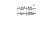
また、例えば上述の動作モード記憶部220に記憶される動作モードの移行条件は任意である。例えば図22に示すように、決定部250は、待ち時間がt2以下の場合は、プロセッサ100の動作モードを上述の第2モードに決定し、待ち時間がt2を超えてt3未満の場合は、プロセッサ100の動作モードを、DVFSによる周波数制御が行われる第3モードに決定し、待ち時間がt3以上の場合は、プロセッサ100の動作モードを上述の第1モードに決定することもできる。図22の例も、決定部250は、待ち時間が所定の時間長(ここではt2)を越える場合は、プロセッサ100の動作モードを第1モードに決定する一方、待ち時間が所定の時間長以下の場合は、プロセッサ100の動作モードを第2モードに決定するという概念に含まれる。
Further, for example, the operation mode transition condition stored in the above-described operation
また、上述の各実施形態では、プロセッサ100は、それぞれが揮発性のメモリで構成されるレジスタ120およびキャッシュメモリ140を有しているが、これに限らず、例えばプロセッサ100が、キャッシュメモリ140を有しない構成であってもよい。この構成であれば、キャッシュメモリ140に記憶されたデータのフラッシュ処理を省略できる。また、レジスタ120やキャッシュメモリ140が不揮発性のメモリで構成されてもよい。この構成であれば、レジスタ120やキャッシュメモリ140に記憶されたデータの退避処理および復帰処理を省略できる。
In each of the above-described embodiments, the
さらに、上述したOS(200,300,400,500,600)の機能の少なくとも一部が、プロセッサ100以外のハードウェアで実現される構成であってもよい。例えば図23に示すように、第1実施形態のOS200の機能が、プロセッサ100とは別のハードウェアであるタイマー管理部201で実現することもできる。
Furthermore, a configuration in which at least a part of the functions of the OS (200, 300, 400, 500, 600) described above is realized by hardware other than the
図24は、タイマー管理部201のCPU30が、プログラムを実行することにより実現される機能の構成と、タイマー管理部201が備えるハードウェアとを示すブロック図である。図24に示すように、タイマー管理部201が備えるハードウェアには、CPU30と、第1記憶部210と、動作モード記憶部220とが含まれる。また、図24に示すように、CPU30がプログラムを実行することにより実現される機能は、状態検出部230、算出部240、決定部250、維持部260、一時停止部270および復帰部280である。図23および図24の例では、タイマー管理部201を動作切替装置として捉えることができる。また、図24においては、タイマー管理部201が備えるハードウェアとタイマー管理部201上で動作するOS、OS上で動作する1または複数のプロセスをタイマー管理部201が含む表現としている。
FIG. 24 is a block diagram illustrating a configuration of functions realized by the
なお、図23および図24の例に限らず、例えばOS200の一部の機能のみがプロセッサ100とは別のハードウェアで実現され、他の機能はOS200上で実現されてもよい。他の実施形態(第2実施形態〜第5実施形態)についても同様である。
23 and 24, for example, only a part of the functions of the
100 プロセッサ
110 第3記憶部
120 レジスタ
140 キャッシュメモリ
201 タイマー管理部
210 第1記憶部
220 動作モード記憶部
230 状態検出部
240 算出部
250 決定部
260 維持部
270 一時停止部
280 復帰部
310 第4記憶部
311 割り込み待ち通知部
313 登録削除部
320 第5記憶部
325 算出部
365 一時停止部
370 復帰部
380 割り込み処理部
390 割り込み待ち解除部
415 登録削除部
417 更新部
500 バス
565 一時停止部
570 復帰部
580 変更部
665 一時停止部
670 復帰部
680 変更部
700 再開制御部
710 第2記憶部
720 再開時間設定部
730 再開部
800 割り込み管理部
810 割り込み管理設定部
820 割り込み検出部
830 再開部
900 記憶領域
100
Claims (8)
割り込み処理の種別を示す割り込み種別と、当該割り込み種別の割り込み待ちが発生した時刻とを記憶する第4記憶部と、
前記割り込み種別と、当該割り込み種別に対応する割り込み待ち時間とを記憶する第5記憶部と、
前記状態検出部で前記アイドル状態が検出されたとき、前記第4記憶部に記憶された情報と、前記第5記憶部に記憶された情報に基づいて、現在時刻から、次の前記割り込み処理が開始されるまでの時間長を示す待ち時間を算出する算出部と、
前記算出部で算出された前記待ち時間に応じて、前記処理装置の動作モードを決定する決定部と、を備える、
ことを特徴とする動作切替装置。 A state detection unit that detects an idle state in which a processing device capable of executing one or more processes is not executing the process;
A fourth storage unit that stores an interrupt type indicating a type of interrupt processing and a time when an interrupt wait of the interrupt type occurs;
A fifth storage unit for storing the interrupt type and an interrupt waiting time corresponding to the interrupt type;
When the idle state is detected by the state detection unit , the next interrupt processing is performed from the current time based on the information stored in the fourth storage unit and the information stored in the fifth storage unit. A calculation unit for calculating a waiting time indicating a length of time until the start,
A determination unit that determines an operation mode of the processing device according to the waiting time calculated by the calculation unit;
An operation switching device characterized by that.
ことを特徴とする請求項1に記載の動作切替装置。 When the waiting time calculated by the calculating unit exceeds a predetermined time length, the determining unit changes the operation mode to a first mode in which the operation of the processing device is temporarily stopped to enter a power saving state. On the other hand, when the waiting time is equal to or shorter than the predetermined time length, the operation mode is determined as a second mode in which the processing device maintains the idle state.
The operation switching device according to claim 1.
前記割り込み処理が開始されるときに、前記一時停止部により節電状態にされた前記処理装置の動作を再開させて前記第1モードを解除する再開部と、
割り込み待ちが発生したときに、当該割り込み待ちになった前記割り込み種別と、当該割り込み待ちが発生した時刻とを前記第4記憶部に登録する一方、割り込み処理が開始されるときに、割り込み待ちが解除される前記割り込み種別と、当該割り込み種別の割り込み待ちが発生した時刻とを、前記第4記憶部から削除する登録削除部と、を備える、
ことを特徴とする請求項1または2に記載の動作切替装置。 When the determination unit determines the operation mode to be the first mode, a temporary stop unit that temporarily stops the operation of the processing device and puts into a power saving state;
When the interrupt process is started, a resuming unit that resumes the operation of the processing device that has been put into a power saving state by the temporary suspension unit and releases the first mode;
When an interrupt wait occurs, the type of interrupt that waited for the interrupt and the time when the interrupt wait occurred are registered in the fourth storage unit. A registration deletion unit that deletes from the fourth storage unit the interrupt type to be released and the time at which the interrupt of the interrupt type has occurred.
The operation switching device according to claim 1 or 2 , characterized in that.
ことを特徴とする請求項1乃至3のうちの何れか1項に記載の動作切替装置。 An interrupt waiting time is determined from the time when the interrupt processing specified by the interrupt type is started and the time when the interrupt waiting for the interrupt processing occurs, and the fifth storage unit is obtained using the determined interrupt waiting time. An update unit that updates the interrupt waiting time stored in
The operation switching device according to any one of claims 1 to 3, wherein the operation switching device according to any one of claims 1 to 3 is provided.
ことを特徴とする請求項1に記載の動作切替装置。 When the determining unit determines the operation mode to be the second mode, the determining unit further includes a maintaining unit that maintains the idle state of the processing device.
The operation switching device according to claim 1 .
ことを特徴とする請求項2に記載の動作切替装置。 A changing unit that changes the predetermined time length according to characteristic information indicating characteristics of the processing device from when the operation of the processing device is temporarily stopped to enter a power saving state until the operation is resumed. Further comprising
The operation switching device according to claim 2.
ことを特徴とする請求項6に記載の動作切替装置。 The characteristic information is power consumption of the processing device.
The operation switching device according to claim 6.
前記アイドル状態検出部で前記アイドル状態が検出されたとき、割り込み処理の種別を示す割り込み種別と、当該割り込み種別の割り込み待ちが発生した時刻とを記憶する第4記憶部に記憶された情報と、前記割り込み種別と、当該割り込み種別に対応する割り込み待ち時間とを記憶する第5記憶部に記憶された情報に基づいて、次の前記割り込み処理が開始されるまでの時間長を示す待ち時間を算出する手順と、
前記算出部で算出された前記待ち時間に応じて、前記処理装置の動作モードを決定する手順と、をコンピュータに実行させるためのプログラム。 A procedure for detecting an idle state in which a processing apparatus capable of executing one or more processes is not executing the process;
When the idle state is detected by the idle state detection unit, information stored in a fourth storage unit that stores an interrupt type indicating a type of interrupt processing and a time when an interrupt of the interrupt type is generated; Based on the information stored in the fifth storage unit that stores the interrupt type and the interrupt wait time corresponding to the interrupt type, a wait time indicating the length of time until the next interrupt process is started is calculated. And the steps to
A program for causing a computer to execute a procedure for determining an operation mode of the processing device according to the waiting time calculated by the calculation unit.
Priority Applications (4)
| Application Number | Priority Date | Filing Date | Title |
|---|---|---|---|
| JP2011065704A JP5284401B2 (en) | 2011-03-24 | 2011-03-24 | Operation switching device and program |
| US13/345,824 US8868952B2 (en) | 2011-03-24 | 2012-01-09 | Controller and program product |
| TW101105893A TWI468928B (en) | 2011-03-24 | 2012-02-22 | Controller and program product therefor |
| CN201210080362.7A CN102722234B (en) | 2011-03-24 | 2012-03-23 | Controller and program product |
Applications Claiming Priority (1)
| Application Number | Priority Date | Filing Date | Title |
|---|---|---|---|
| JP2011065704A JP5284401B2 (en) | 2011-03-24 | 2011-03-24 | Operation switching device and program |
Publications (2)
| Publication Number | Publication Date |
|---|---|
| JP2012203518A JP2012203518A (en) | 2012-10-22 |
| JP5284401B2 true JP5284401B2 (en) | 2013-09-11 |
Family
ID=46878350
Family Applications (1)
| Application Number | Title | Priority Date | Filing Date |
|---|---|---|---|
| JP2011065704A Expired - Fee Related JP5284401B2 (en) | 2011-03-24 | 2011-03-24 | Operation switching device and program |
Country Status (4)
| Country | Link |
|---|---|
| US (1) | US8868952B2 (en) |
| JP (1) | JP5284401B2 (en) |
| CN (1) | CN102722234B (en) |
| TW (1) | TWI468928B (en) |
Cited By (2)
| Publication number | Priority date | Publication date | Assignee | Title |
|---|---|---|---|---|
| JP2013069110A (en) * | 2011-09-22 | 2013-04-18 | Toshiba Corp | Control device and program |
| US9326812B2 (en) | 2012-01-25 | 2016-05-03 | Covidien Lp | Portable surgical instrument |
Families Citing this family (25)
| Publication number | Priority date | Publication date | Assignee | Title |
|---|---|---|---|---|
| JP5674611B2 (en) | 2011-09-22 | 2015-02-25 | 株式会社東芝 | Control system, control method and program |
| JP5674613B2 (en) | 2011-09-22 | 2015-02-25 | 株式会社東芝 | Control system, control method and program |
| JP2013149093A (en) | 2012-01-19 | 2013-08-01 | Toshiba Corp | Control device, control method, program, and electronic apparatus |
| JP6007642B2 (en) * | 2012-01-26 | 2016-10-12 | 株式会社リコー | Information processing apparatus, power saving control method, power saving control program |
| JP6113538B2 (en) | 2012-03-23 | 2017-04-12 | 株式会社東芝 | Control device, control method, program, and semiconductor device |
| JP5677376B2 (en) | 2012-07-06 | 2015-02-25 | 株式会社東芝 | Memory control device, semiconductor device, and system board |
| JP5787852B2 (en) | 2012-09-07 | 2015-09-30 | 株式会社東芝 | Control device, information processing device, control method, and program |
| JP5696110B2 (en) | 2012-09-19 | 2015-04-08 | 株式会社東芝 | Power supply system, power supply control device, and program |
| JP5802637B2 (en) | 2012-09-21 | 2015-10-28 | 株式会社東芝 | Information processing apparatus, information processing method, and program |
| US8909836B2 (en) * | 2012-10-08 | 2014-12-09 | Andes Technology Corporation | Interrupt controller, apparatus including interrupt controller, and corresponding methods for processing interrupt request event(s) in system including processor(s) |
| JP6071647B2 (en) | 2013-02-28 | 2017-02-01 | 株式会社東芝 | Information processing apparatus, operation state control method, and program |
| JP6116941B2 (en) | 2013-02-28 | 2017-04-19 | 株式会社東芝 | Information processing device |
| JP6087662B2 (en) | 2013-02-28 | 2017-03-01 | 株式会社東芝 | Control device, control program, and information processing system |
| JP6054203B2 (en) | 2013-02-28 | 2016-12-27 | 株式会社東芝 | Information processing apparatus, device control method, and program |
| JP2015064676A (en) | 2013-09-24 | 2015-04-09 | 株式会社東芝 | Information processing apparatus, semiconductor device, information processing method, and program |
| US20160216756A1 (en) * | 2013-11-29 | 2016-07-28 | Wei Yang | Power management in computing devices |
| US9507706B2 (en) * | 2013-12-03 | 2016-11-29 | Sandisk Technologies Llc | Memory system controller including a multi-resolution internal cache |
| JP6184891B2 (en) | 2014-03-12 | 2017-08-23 | 東芝メモリ株式会社 | Information processing apparatus, semiconductor chip, information processing method, and program |
| US9354930B2 (en) * | 2014-04-11 | 2016-05-31 | Telefonaktiebolaget Lm Ericsson (Publ) | Scheduling of global voltage/frequency scaling switches among asynchronous dataflow dependent processors |
| JP2017111745A (en) * | 2015-12-18 | 2017-06-22 | ルネサスエレクトロニクス株式会社 | Semiconductor device, semiconductor system, and control method of semiconductor device |
| US11625267B2 (en) * | 2017-08-02 | 2023-04-11 | Felica Networks, Inc. | Information processing apparatus and information processing method for changing contents of a process to be performed after an interrupt is detected |
| US10747298B2 (en) * | 2017-11-29 | 2020-08-18 | Advanced Micro Devices, Inc. | Dynamic interrupt rate control in computing system |
| CN114020140B (en) * | 2020-02-12 | 2023-11-28 | 地平线(上海)人工智能技术有限公司 | Method and device for controlling hardware module, electronic equipment and storage medium |
| EP3929740A1 (en) * | 2020-06-26 | 2021-12-29 | Siemens Aktiengesellschaft | Method for orchestrating a container-based application on a terminal |
| TWI879116B (en) * | 2023-09-27 | 2025-04-01 | 群聯電子股份有限公司 | Memory control method, memory storage device and memory control circuit unit |
Family Cites Families (10)
| Publication number | Priority date | Publication date | Assignee | Title |
|---|---|---|---|---|
| JP2644348B2 (en) * | 1989-11-30 | 1997-08-25 | 株式会社東芝 | Computer system |
| JP3610930B2 (en) | 2001-07-12 | 2005-01-19 | 株式会社デンソー | Operating system, program, vehicle electronic control unit |
| JP3852703B2 (en) | 2001-08-29 | 2006-12-06 | アナログ・デバイシズ・インコーポレーテッド | Method and apparatus for timing and event processing in a wireless system |
| US7360106B2 (en) | 2004-08-05 | 2008-04-15 | Matsushita Electric Industrial Co., Ltd. | Power-saving processing unit, power-saving processing method and program record medium |
| US7383457B1 (en) * | 2005-03-23 | 2008-06-03 | Apple Inc. | Adaptive power-reduction mode |
| WO2007090431A1 (en) * | 2006-02-09 | 2007-08-16 | Freescale Semiconductor, Inc. | Electronic apparatus and method of conserving energy |
| CN101097482A (en) * | 2006-06-30 | 2008-01-02 | 佛山市顺德区顺达电脑厂有限公司 | Operation mode control system and method thereof |
| JP2008243220A (en) * | 2008-04-28 | 2008-10-09 | Renesas Technology Corp | Information processing communication device |
| JP5109935B2 (en) * | 2008-11-10 | 2012-12-26 | 富士通株式会社 | Processor system operating method and processor system |
| JP4644747B1 (en) * | 2009-11-02 | 2011-03-02 | パナソニック株式会社 | Information processing apparatus, control method, and control program |
-
2011
- 2011-03-24 JP JP2011065704A patent/JP5284401B2/en not_active Expired - Fee Related
-
2012
- 2012-01-09 US US13/345,824 patent/US8868952B2/en not_active Expired - Fee Related
- 2012-02-22 TW TW101105893A patent/TWI468928B/en not_active IP Right Cessation
- 2012-03-23 CN CN201210080362.7A patent/CN102722234B/en not_active Expired - Fee Related
Cited By (2)
| Publication number | Priority date | Publication date | Assignee | Title |
|---|---|---|---|---|
| JP2013069110A (en) * | 2011-09-22 | 2013-04-18 | Toshiba Corp | Control device and program |
| US9326812B2 (en) | 2012-01-25 | 2016-05-03 | Covidien Lp | Portable surgical instrument |
Also Published As
| Publication number | Publication date |
|---|---|
| CN102722234B (en) | 2015-01-07 |
| US20120246501A1 (en) | 2012-09-27 |
| US8868952B2 (en) | 2014-10-21 |
| JP2012203518A (en) | 2012-10-22 |
| TWI468928B (en) | 2015-01-11 |
| CN102722234A (en) | 2012-10-10 |
| TW201239610A (en) | 2012-10-01 |
Similar Documents
| Publication | Publication Date | Title |
|---|---|---|
| JP5284401B2 (en) | Operation switching device and program | |
| US10503542B2 (en) | Systems, methods and devices for work placement on processor cores | |
| JP5469940B2 (en) | Computer system, virtual machine monitor, and virtual machine monitor scheduling method | |
| US10281970B2 (en) | Control device, system, and computer program product | |
| JP5834939B2 (en) | Program, virtual machine control method, information processing apparatus, and information processing system | |
| US20110276690A1 (en) | Distributed resource contention detection | |
| US20110271126A1 (en) | Data processing system | |
| JP5347451B2 (en) | Multiprocessor system, conflict avoidance program, and conflict avoidance method | |
| JP2010271930A (en) | Multi-core processor system | |
| US20110276542A1 (en) | Management of latency and throughput in a cluster file system | |
| CN101542442A (en) | Multiprocessor control unit, its control method, and integrated circuit | |
| JP2016506576A (en) | Integrated circuit idle phase prediction. | |
| TW201205441A (en) | Multi-CPU domain mobile electronic device and operation method thereof | |
| JP2016189049A (en) | Semiconductor device and method for controlling the same | |
| JPWO2012001776A1 (en) | Multi-core system, scheduling method and scheduling program | |
| US11822408B2 (en) | Computer-readable recording medium storing program and management method | |
| US10802832B2 (en) | Information processing device and method of controlling computers | |
| JP6547363B2 (en) | Management device, control method of management device, and program | |
| CN102385529B (en) | Multi-CPU (Central Processing Unit) domain mobile electronic device and operating method thereof | |
| Prasasta et al. | Co-Design of a Power State-Aware Scheduler and an Intelligent Power Manager for Energy-Efficient HPC Systems | |
| JP5876184B2 (en) | Control device, information processing system, and program | |
| US10387190B2 (en) | System and method of executing a plurality of threads using thread switching on execution time-out using instruction re-write | |
| JP5591031B2 (en) | Multiprocessor system, control method thereof, and program | |
| JP2015038780A (en) | Controller, information processing system and program | |
| TW201106147A (en) | Power-saving computer system, graphics processing module, and the power saving method thereof |
Legal Events
| Date | Code | Title | Description |
|---|---|---|---|
| A131 | Notification of reasons for refusal |
Free format text: JAPANESE INTERMEDIATE CODE: A131 Effective date: 20121113 |
|
| A521 | Written amendment |
Free format text: JAPANESE INTERMEDIATE CODE: A523 Effective date: 20130115 |
|
| A131 | Notification of reasons for refusal |
Free format text: JAPANESE INTERMEDIATE CODE: A131 Effective date: 20130212 |
|
| TRDD | Decision of grant or rejection written | ||
| A01 | Written decision to grant a patent or to grant a registration (utility model) |
Free format text: JAPANESE INTERMEDIATE CODE: A01 Effective date: 20130507 |
|
| A61 | First payment of annual fees (during grant procedure) |
Free format text: JAPANESE INTERMEDIATE CODE: A61 Effective date: 20130529 |
|
| R151 | Written notification of patent or utility model registration |
Ref document number: 5284401 Country of ref document: JP Free format text: JAPANESE INTERMEDIATE CODE: R151 |
|
| S111 | Request for change of ownership or part of ownership |
Free format text: JAPANESE INTERMEDIATE CODE: R313111 |
|
| R350 | Written notification of registration of transfer |
Free format text: JAPANESE INTERMEDIATE CODE: R350 |
|
| LAPS | Cancellation because of no payment of annual fees |