JP5264499B2 - Apparatus and method for compensating color shift in a display - Google Patents
Apparatus and method for compensating color shift in a display Download PDFInfo
- Publication number
- JP5264499B2 JP5264499B2 JP2008545192A JP2008545192A JP5264499B2 JP 5264499 B2 JP5264499 B2 JP 5264499B2 JP 2008545192 A JP2008545192 A JP 2008545192A JP 2008545192 A JP2008545192 A JP 2008545192A JP 5264499 B2 JP5264499 B2 JP 5264499B2
- Authority
- JP
- Japan
- Prior art keywords
- sub
- pixels
- frame
- row
- pixel
- Prior art date
- Legal status (The legal status is an assumption and is not a legal conclusion. Google has not performed a legal analysis and makes no representation as to the accuracy of the status listed.)
- Expired - Fee Related
Links
Images


Classifications
-
- G—PHYSICS
- G09—EDUCATION; CRYPTOGRAPHY; DISPLAY; ADVERTISING; SEALS
- G09G—ARRANGEMENTS OR CIRCUITS FOR CONTROL OF INDICATING DEVICES USING STATIC MEANS TO PRESENT VARIABLE INFORMATION
- G09G3/00—Control arrangements or circuits, of interest only in connection with visual indicators other than cathode-ray tubes
- G09G3/20—Control arrangements or circuits, of interest only in connection with visual indicators other than cathode-ray tubes for presentation of an assembly of a number of characters, e.g. a page, by composing the assembly by combination of individual elements arranged in a matrix no fixed position being assigned to or needed to be assigned to the individual characters or partial characters
- G09G3/34—Control arrangements or circuits, of interest only in connection with visual indicators other than cathode-ray tubes for presentation of an assembly of a number of characters, e.g. a page, by composing the assembly by combination of individual elements arranged in a matrix no fixed position being assigned to or needed to be assigned to the individual characters or partial characters by control of light from an independent source
- G09G3/36—Control arrangements or circuits, of interest only in connection with visual indicators other than cathode-ray tubes for presentation of an assembly of a number of characters, e.g. a page, by composing the assembly by combination of individual elements arranged in a matrix no fixed position being assigned to or needed to be assigned to the individual characters or partial characters by control of light from an independent source using liquid crystals
- G09G3/3611—Control of matrices with row and column drivers
- G09G3/3685—Details of drivers for data electrodes
- G09G3/3688—Details of drivers for data electrodes suitable for active matrices only
-
- G—PHYSICS
- G09—EDUCATION; CRYPTOGRAPHY; DISPLAY; ADVERTISING; SEALS
- G09G—ARRANGEMENTS OR CIRCUITS FOR CONTROL OF INDICATING DEVICES USING STATIC MEANS TO PRESENT VARIABLE INFORMATION
- G09G2310/00—Command of the display device
- G09G2310/02—Addressing, scanning or driving the display screen or processing steps related thereto
- G09G2310/0264—Details of driving circuits
- G09G2310/0297—Special arrangements with multiplexing or demultiplexing of display data in the drivers for data electrodes, in a pre-processing circuitry delivering display data to said drivers or in the matrix panel, e.g. multiplexing plural data signals to one D/A converter or demultiplexing the D/A converter output to multiple columns
-
- G—PHYSICS
- G09—EDUCATION; CRYPTOGRAPHY; DISPLAY; ADVERTISING; SEALS
- G09G—ARRANGEMENTS OR CIRCUITS FOR CONTROL OF INDICATING DEVICES USING STATIC MEANS TO PRESENT VARIABLE INFORMATION
- G09G2320/00—Control of display operating conditions
- G09G2320/02—Improving the quality of display appearance
- G09G2320/0209—Crosstalk reduction, i.e. to reduce direct or indirect influences of signals directed to a certain pixel of the displayed image on other pixels of said image, inclusive of influences affecting pixels in different frames or fields or sub-images which constitute a same image, e.g. left and right images of a stereoscopic display
-
- G—PHYSICS
- G09—EDUCATION; CRYPTOGRAPHY; DISPLAY; ADVERTISING; SEALS
- G09G—ARRANGEMENTS OR CIRCUITS FOR CONTROL OF INDICATING DEVICES USING STATIC MEANS TO PRESENT VARIABLE INFORMATION
- G09G2320/00—Control of display operating conditions
- G09G2320/02—Improving the quality of display appearance
- G09G2320/0242—Compensation of deficiencies in the appearance of colours
Abstract
Description
本発明は、アクティブマトリックスディスプレイモジュールおよびアクティブマトリックスディスプレイモジュールに実装されたカラーシフト補償方法に関する。 The present invention relates to an active matrix display module and a color shift compensation method implemented in the active matrix display module.
アクティブマトリクスLCD(AMLCD)用の駆動回路は、2個の部分、すなわちソースドライバおよびゲートドライバに分けることができる。ゲートドライバは、特定の行の全てのピクセルを選択するまたは非選択にするためにオンガラストランジスタのゲートを制御する。各ピクセルは、3個のサブピクセル(赤、緑、青)から成り、各サブピクセルは、固有の蓄積キャパシタを有する。ソースドライバは、電流によって選択した行のすべてのサブピクセルに、各色に必要な強度に対応する電圧レベルを供給する。最終的な色は、人間の目における3原色(赤、緑、青)の組み合わせを1個の色に混ぜ合わせる能力に基づいて得られる。 The drive circuit for an active matrix LCD (AMLCD) can be divided into two parts: a source driver and a gate driver. The gate driver controls the gate of the on-glass transistor to select or deselect all pixels in a particular row. Each pixel consists of three subpixels (red, green, blue), each subpixel having its own storage capacitor. The source driver supplies a voltage level corresponding to the intensity required for each color to all subpixels in the row selected by the current. The final color is obtained based on the ability to mix the combination of the three primary colors (red, green, blue) in the human eye into a single color.
ゲートドライバによって先に選択した行が非選択にされるとき、この行の全てのサブピクセルは隔離され、各サブピクセルの電圧レベルは、蓄積キャパシタおよびピクセルキャパシタによって維持される。すべてのディスプレイ行が正確に1回選択される期間を、一般的に‘フレーム’と呼ばれる。 When the previously selected row is deselected by the gate driver, all subpixels in this row are isolated and the voltage level of each subpixel is maintained by the storage capacitor and the pixel capacitor. The period during which all display rows are selected exactly once is commonly referred to as a 'frame'.
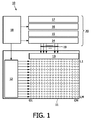
図1は、アクティブマトリックスLTPS(低温ポリシリコン)ディスプレイモジュール10の例の略図である。このLTPSディスプレイモジュール10においては、ゲートドライバ回路12をディスプレイガラス11に直接取り付ける。このことはゲートドライバ12が一般的にディスプレイガラス11に簡単に実装することのできる回路のみから構成されているため、可能となる。理論的には、ゲートドライバは、別個のチップによって取り付けることもできる。ソースドライバは、オンガラスまたは別個のチップに統合することができる。図1には、デマルチプレクサ13をディスプレイガラス11に統合した実施形態を示す。マルチプレクサ14、ソース出力ドライバ15、ラッチ16、バッファ17および制御回路18を個別のソースドライバチップ20内に実現する。ディスプレイパネルは、この場合、N列およびM行を有する。多重化率が1:3の場合、ディスプレイパネル11を有するソースドライバチップ20に接続するのに、N/3のソースドライバライン19のみ必要となる。LTPS技術によってディスプレイガラスにデマルチプレクサを統合することが可能となり、必要となるソースドライバライン19の数を劇的に減らすことができる。LTPSは例としてのみ示している。後述する本発明はLTPSに限定されるものではない。
FIG. 1 is a schematic diagram of an example of an active matrix LTPS (low temperature polysilicon)
ソースドライバ回路をチップ上に統合する場合、該オンガラスデマルチプレクシング(逆多重化)方法により、特定サイズのディスプレイを駆動するのに必要なソース出力パッドの量が減る。もしくは、換言すると、単一のチップにより駆動することのできるディスプレイサイズを増大させることができる。マルチプレクシングの場合、例えば多重化率1:3の場合は1つの多重化グループ当たり3つのサブピクセル、もしくは多重化率1:6の場合は1つの多重化グループ当たり6つのサブピクセルといったようにソースラインをグループ化する。ある行が選択された場合、その行にあるサブピクセルは全く同時には充電されないが、1つのグループのソースラインは順次に充電される。例えば多重化率1:3の場合、第1の全ての赤サブピクセルが選択され、次に全ての緑サブピクセルが選択され、最後に全ての青サブピクセルが選択される。この後、この行は非選択にされ、次の行が選択され再び赤サブピクセルが充電されるといったようになる。この場合を図2に示した。この図では2個の行RN+1およびRN、および3個の列n−1、n、n+1を示す。各ピクセルは、上述のように3個のサブピクセルを有している。図2において、列n−1のサブピクセルは、(赤)Rn−1、(緑)Gn−1、(青)Bn−1として示す。ソースドライバライン19はSn−1,Sn,Sn+1として示す。デマルチプレクサ13のスイッチには参照符号21を、デマルチプレクサ選択ラインには参照符号22を付けて示す。Cpは2個の隣接するソースライン間にある寄生コンデンサであり、Cpixはピクセルコンデンサである。さらに、各サブピクセルは、各行および列の交点にサブピクセル選択トランジスタを有する。このようなサブピクセル選択トランジスタに参照符号23を付けて示す。
When source driver circuitry is integrated on a chip, the on-glass demultiplexing method reduces the amount of source output pads required to drive a particular size display. Or, in other words, the display size that can be driven by a single chip can be increased. In the case of multiplexing, for example, if the multiplexing rate is 1: 3, 3 subpixels per multiplexing group, or if the multiplexing rate is 1: 6, the source is 6 subpixels per multiplexing group. Group lines together. If a row is selected, the subpixels in that row are not charged at the same time, but one group of source lines is charged sequentially. For example, for a multiplexing ratio of 1: 3, all first red subpixels are selected, then all green subpixels are selected, and finally all blue subpixels are selected. After this, this row is deselected, the next row is selected, and the red subpixel is charged again. This case is shown in FIG. The figure shows two rows R N + 1 and R N and three columns n−1, n, n + 1. Each pixel has three subpixels as described above. In FIG. 2, the sub-pixels in column n−1 are shown as (red) R n−1 , (green) G n−1 , (blue) B n−1 . The
デマルチプレクシング方法の問題点は、いわゆるカラーシフトである。行を選択した場合、この行用の全てのオンガラスサブピクセル選択トランジスタに通電する。図3に示すように、あるサブピクセルを充電することは、2個のライン(主に隣接するライン)間の寄生コンデンサCpを経て、隣接するピクセル(前に充電してあるピクセル)に影響する。デマルチプレクサ選択信号を、デマルチプレクサ選択ライン22のすぐ左側に示す。図3においてカラーシフトは、εBおよびεGとして示す。従って、ある行における前回直前に充電したサブピクセルのみが、その行を非選択にしたとき、正しい電圧レベルを有する(図3の場合においては青サブピクセル)。
A problem of the demultiplexing method is so-called color shift. When a row is selected, all on-glass subpixel select transistors for this row are energized. As shown in FIG. 3, it is to charge a certain sub-pixel, influence the two lines through the parasitic capacitor C p between (mainly the adjacent lines to), (are charged before the pixel) neighboring pixels To do. A demultiplexer select signal is shown immediately to the left of the demultiplexer
カラーシフト効果を補償するための先端技術は、フレームからフレームへとピクセルオーダ選択を回転させることである。この方法によれば、最後に充電した特定の行のピクセル(正しい色となるピクセル)が、各異なるフレームに存在する。最後に選択したサブピクセルの色は正しくなり、各サブピクセルにおけるエラーは、多重化率1:3の場合3つのフレーム間で部分的に平均化される(多重化率1:6の場合は6つのフレーム)。フレーム周波数および多重化係数によって、エラーを平均化するのに必要となるフレーム量は長くなりすぎることがあり、ディスプレイにおいてフリッカーとして受け取られることがある。特に高い多重化率にいては、フリッカーを避けるために高いフレーム周波数を適用しなければならない。 An advanced technique for compensating for color shift effects is to rotate the pixel order selection from frame to frame. According to this method, the last charged pixel in a specific row (a pixel with the correct color) is present in each different frame. The color of the last selected sub-pixel is correct and the error in each sub-pixel is partially averaged between the three frames for a multiplexing rate of 1: 3 (6 for a multiplexing rate of 1: 6). One frame). Depending on the frame frequency and multiplexing factor, the amount of frames required to average the error may be too long and may be received as flicker in the display. Especially at high multiplexing rates, a high frame frequency must be applied to avoid flicker.
この方法の欠点は、カラーシフトが緩慢に(数フレームにわたって)しか補償されないことであり、特定の逸脱が常に残ることである。 The disadvantage of this method is that the color shift is only compensated slowly (over several frames), and certain deviations always remain.
本発明の目的は、より良くかつ高速な色補償スキームを提供することである。 An object of the present invention is to provide a better and faster color compensation scheme.
この目的および他の目的は、請求項1に記載の装置、および請求項8および10に記載の方法により達成される。さらに好適な実施形態を従属項に記載する。
This and other objects are achieved by an apparatus according to
本発明によると、カラーシフトは、サブピクセル用のスマート選択オーダを用いることで補償することができる。本発明によると、補償は2個のフレーム内で行うことができる。カラーシフトは、第1フレームにおいて部分的に補償され、第2フレームにおいて完全に補償される。 According to the present invention, the color shift can be compensated by using a smart selection order for subpixels. According to the present invention, compensation can be performed in two frames. The color shift is partially compensated in the first frame and fully compensated in the second frame.
本発明によれば、ソースドライバおよびゲートドライバを有する駆動回路を備えるアクティブマトリクスモジュールを提供する。さらに、3個のサブピクセルからなるピクセルを有するディスプレイパネルを設ける。サブピクセルは、行および列に配列し、各サブピクセルは行および列の交点に配置したサブピクセル選択トランジスタを備えている。ゲートドライバは、ディスプレイパネルのある行の全てのピクセルを選択するおよび非選択にするために使用し、ソースドライバは、その時点で選択している行の全てのサブピクセルに必要な電圧レベルを供給するのに使用し、この電圧レベルは各色に必要な強度に対応する。デマルチプレクサスイッチは、ディスプレイパネルの行を逆多重化するためにディスプレイパネルに統合する。アクティブマトリクスディスプレイモジュールはさらに、カラーシフトを補償する手段を備えている。これら手段は不要なカラーシフトを補償するために、サブピクセルを選択するための選択オーダを実装している。補償は2個のフレーム間で行う。
他の有利な実施形態を以下に説明する。
According to the present invention, an active matrix module including a driving circuit having a source driver and a gate driver is provided. Further, a display panel having pixels composed of three subpixels is provided. The subpixels are arranged in rows and columns, and each subpixel includes a subpixel selection transistor disposed at the intersection of the row and column. The gate driver is used to select and deselect all pixels in a row of the display panel, and the source driver supplies the required voltage level to all subpixels in the currently selected row. This voltage level corresponds to the intensity required for each color. The demultiplexer switch integrates into the display panel to demultiplex the rows of the display panel. The active matrix display module further comprises means for compensating for the color shift. These means implement a selection order for selecting sub-pixels to compensate for unwanted color shifts. Compensation is performed between two frames.
Other advantageous embodiments are described below.
本発明によると、カラーシフトは、サブピクセルを選択する際に使用するスマート選択オーダによって補償することができる。 In accordance with the present invention, the color shift can be compensated by a smart selection order used in selecting subpixels.
第1フレームにおいて、カラーシフトを部分的に補償し、第2フレームにおいて完全に補償する。この方法によると、フリッカー(従来技術による方法においては存在した)を回避できる。 In the first frame, the color shift is partially compensated and in the second frame is fully compensated. This method avoids flicker (which existed in the prior art methods).
本明細書で提案する本発明の選択オーダは、同時に電力消費を最小化するように選択する。 The selection order of the present invention proposed herein selects to minimize power consumption at the same time.
基本概念は、以下の物理特性に基づく。
1. ある行を選択し、この行におけるサブピクセルnが充電されたと仮定する。この行における隣接サブピクセルn+1および隣接サブピクセルn−1を逆電圧極性で充電する場合(一方を正の電圧に、他方を負の電圧にする)、ピクセルnにおけるカラーシフトは減衰する(部分的に補償される)。
2. ある行を選択し、この行における互いに隣接する2個のサブピクセルを同時に選択すると仮定する。この場合、一方のサブピクセルを充電する電圧レベルは、他方のサブピクセルを充電する電圧レベルに影響を与えない。
3. サブピクセル選択オーダの選択は、あるフレームにおけるカラーシフト絶対値が次のフレームのカラーシフト絶対値と同じであり極性が逆となるように選択することができる。このようにして、カラーシフトは2個のフレーム間で平均化される。
4. ある行を選択し、この行からのサブピクセルnが既に充電されたと仮定する。ここでサブピクセルnに隣接していない次のサブピクセル(例えばサブピクセルn−2,n−3,…またはサブピクセルn+2,n+3,…)が充電している場合、サブピクセルnにおけるカラーシフトは極めて小さくなると考えられる。
The basic concept is based on the following physical properties:
1. Suppose a row is selected and subpixel n in this row is charged. When adjacent subpixel n + 1 and adjacent subpixel n-1 in this row are charged with reverse voltage polarity (one is a positive voltage and the other is a negative voltage), the color shift at pixel n is attenuated (partial). Compensated for).
2. Assume that a row is selected and two adjacent subpixels in this row are selected simultaneously. In this case, the voltage level for charging one subpixel does not affect the voltage level for charging the other subpixel.
3. The selection of the subpixel selection order can be selected so that the color shift absolute value in one frame is the same as the color shift absolute value in the next frame and the polarity is reversed. In this way, the color shift is averaged between the two frames.
4. Assume that a row is selected and that subpixel n from this row has already been charged. If the next subpixel not adjacent to subpixel n is charged (eg, subpixel n-2, n-3,... Or subpixel n + 2, n + 3,...), The color shift at subpixel n is It will be very small.
このスマートカラーシフト補償の2つの異なる実施形態を添付図面につき説明する。 Two different embodiments of this smart color shift compensation will be described with reference to the accompanying drawings.
2つの実施形態について説明する前に、線図的図面の基本的態様を説明する。 Before describing the two embodiments, the basic aspects of the diagrammatic drawings will be described.
各図には、ディスプレイパネル11の一部を示す。ディスプレイパネル11は、3個のサブピクセル(Rn、Gn、Bn)から成るピクセルを有する。サブピクセルは、行ラインと称される行方向(水平方向)に配置する。各サブピクセルは、行と列の交点に配置したサブピクセル選択トランジスタ23を有する。行におけるサブピクセル選択トランジスタ23は、全て個別の、即ち異なるデータライン(垂直/列ライン)に接続する。ゲートドライバ12を使用して、ディスプレイパネル11の行における全てのピクセルを選択するおよび非選択にする。ソースドライバ20は、ディスプレイパネル11のその時点で選択した行におけるすべてのサブピクセルに対する必要とされる電圧レベルを供給し、これら電圧レベルは、各色に必要とされる色の強度に対応する。
In each figure, a part of the
多重化ディスプレイ実装を使用する場合、対応するデマルチプレクサスイッチをディスプレイパネル11のデータラインを逆多重化するためにディスプレイパネル11に統合してもよい。図4Aにデマルチプレクサスイッチを22.1として示す。
If a multiplexed display implementation is used, a corresponding demultiplexer switch may be integrated into the
制御回路18は、デマルチプレクサロジックまたはシーケンサを有するものとし、これにより本発明に関するデマルチプレクサスイッチ21を制御するようにすることもできる。すなわち、制御回路18が正しい信号を供給し、上述の特性を満足するようにデマルチプレクサスイッチ32を切り替えるようにする。
The
本発明の第1実施形態は、1:3の多重化率で設計している。この特定の実施形態においては、上述の特性1、2および3を使用する。本発明によれば、本明細書に記載したもの以外の選択オーダを使用することも可能であることに留意されたい。
The first embodiment of the present invention is designed with a multiplexing rate of 1: 3. In this particular embodiment,
以下に、ある可能なソリューションについて説明し、この場合、ピクセルの充電を以下のステップに分割する。すなわち、
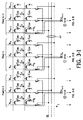
フレーム1(図4A〜4C参照):
1. 行RNをゲートドライバ12によって選択する。
2. 行RNの多重化グループの中間にある全てのサブピクセル(Gn−1、Gn、Gn+1)を充電する(図4A参照)。これは、デマルチプレクサ選択ライン22.1が短期間ロジック1となるように対応するデマルチプレクサ選択ライン22.1にそれぞれ信号パルスmuxsel<1>を供給することによって行う。ソースドライバライン19の右脇に記したように、サブピクセルGn−1は正電圧に、サブピクセルGnは負電圧に、サブピクセルGn+1は正電圧に充電することに注意されたい。
3. 隣接するサブピクセルのうち一方(図示の実施例においてはサブピクセルBn−1)は、一方の電圧極性(正と仮定する)で充電する。これは、すなわち、対応するデマルチプレクサ選択ライン22.2のそれぞれの信号パルスmuxsel<2>は短時間でロジック1となるためである。特性2の利点を利用するためには、隣接する多重化グループにおける隣接するサブピクセル(図示の実施例においてはサブピクセルRn)を同時に選択する(この方法によると2つのサブピクセル(Bn−1およびRn)は互いに影響しない)(図4B参照、VRはVBに影響されない)。
4. つぎに、中央サブピクセル(図示の実施例においてはサブピクセルGn−1)における他方の隣り合ったサブピクセル(図示の実施例においてはサブピクセルRn−1)を、逆の電圧極性(負と仮定する)に充電する。これは、すなわち、対応するデマルチプレクサ選択ライン22.0のそれぞれの信号パルスmuxsel<0>は短時間でロジック1となるためである。これは特性1の利点を利用する(このようにして、中央サブピクセル(図示の実施例においてはサブピクセルGn−1)への影響が部分的に減衰する)。ステップ2のように、2個の互いに隣接する多重化グループ間における2個の隣接するサブピクセル(BnおよびRn+1)を同時に選択する。このようにして、これら2個のサブピクセル(BnおよびRn+1)は互いに影響しない。最終的に、行RNの全てのピクセルを充電し、カラーシフトの影響を僅かに受けるサブピクセルは中央のサブピクセルのみとなる(図4C参照)。
5. 上述のステップを、ディスプレイ全体が処理されるまで、全ての行について繰り返す。
In the following, one possible solution is described, in which case the pixel charging is divided into the following steps: That is,
Frame 1 (see FIGS. 4A-4C):
1. The row R N is selected by the
2. Row R N all the subpixels in the middle of a multiplexing group (G n-1, G n , G n + 1) is charged (see FIG. 4A). This is done by supplying the respective signal pulse muxsel <1> to the corresponding demultiplexer selection line 22.1 so that the demultiplexer selection line 22.1 becomes
3. One of the adjacent sub-pixels (sub-pixel B n-1 in the illustrated embodiment) is charged with one voltage polarity (assuming positive). This is because each signal pulse muxsel <2> on the corresponding demultiplexer selection line 22.2 becomes
4). Next, the other adjacent sub-pixel (sub-pixel R n-1 in the illustrated embodiment) in the central sub-pixel (sub-pixel G n-1 in the illustrated embodiment) is set to a reverse voltage polarity (negative Charge). This is because each signal pulse muxsel <0> on the corresponding demultiplexer selection line 22.0 becomes
5. The above steps are repeated for all rows until the entire display has been processed.
この方法によってフレーム1が完了する。
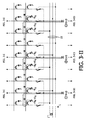
フレーム2(図5A〜5C参照):
6. カラーシフトを補償するために、この第2フレームでは中央サブピクセル(Gn)に隣接する2個のサブピクセル(RnおよびBn)の極性を反転する。中央サブピクセル(Gn)はフレーム1と同じ極性で充填する。隣接ピクセルの選択オーダは、電流消費を抑えるために、前述のフレームとは異ならせる。すなわち、サブピクセルRnを選択する前にサブピクセルBnを選択する。ソースライン19を反対の電圧極性に充電する必要はない(図5A〜5C参照)。
This method completes
Frame 2 (see FIGS. 5A-5C):
6). To compensate for color shift, reversing the polarity of the two sub-pixels in this second frame adjacent to the central sub-pixel (G n) (R n and B n). The center sub-pixel (G n ) is filled with the same polarity as
図4Cおよび5Cは、カラーシフトεBおよびεRがフレーム1およびフレーム2にわたって平均化することによって補償されることを示している(上述の特性3参照)。
7. 全てのディスプレイを対象とするまで全ての行についてステップ6を繰り返す。
4C and 5C show that the color shifts εB and εR are compensated by averaging over
7).
このようにしてフレーム2は完了し、カラーシフトは補償される。
フレーム3および4(図6A〜6Cおよび図7A〜7C参照):
8. ディスプレイパネル11の液晶の劣化を防ぐために、各サブピクセルのDC値は平均して0Vとする。各サブピクセルのDCレベルを消去するために、2個のフレーム1および2を反転した極性において繰り返さなくてはならない(図6A〜6Cおよび図7A〜7C参照)。
In this way,
8). In order to prevent deterioration of the liquid crystal of the
ステップ8(第3フレームおよび第4フレーム中に実行する)は任意であることに留意されたい。 Note that step 8 (performed during the third and fourth frames) is optional.
本発明の第2の実施形態は、1:6の多重化率(muxレート)用に設計する。この特性の実施形態においては、上述の特性1、3および4を使用する。本発明によれば、本明細書に記載したもの以外の選択オーダを使用することも可能であることに留意されたい。
The second embodiment of the present invention is designed for a 1: 6 multiplexing rate. In the embodiment of this characteristic, the above-mentioned
以下に、ある可能なソリューションについて説明する。ここではピクセルの充電を、以下のステップに分割する:
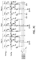
フレーム1(図8A〜8F参照)
1. ゲートドライバ12によって行RNを選択する。
2. 各逆多重化グループの3個のサブピクセルを連続で選択する(それぞれ例えばサブピクセル5,3,1との順に選択する)。図8Aにおいては、サブピクセル5を選択する。図8Bにおいてはサブピクセル3を、図8Cにおいてはサブピクセル1を選択する。選択オーダは以下のようにする、すなわちすべての第2サブピクセル(図8Aから8C参照)を選択し、他のサブピクセルを後に選択する(以下のステップ3参照)。この方法では、特性4を使用する。多重化レート1:3の時のように、2個の逆多重化グループは常に逆ピクセル極性を有する。
3. サブピクセル4,2,6を、順次に充電するが、各サブピクセル5,3,1が左右に逆極性を持ったサブピクセルを有するようにする(特性1を使用)(図8D〜8F参照)。
4. 上述のステップ1〜3を、全てのディスプレイを対象とするまで全ての行について繰り返す。
The following describes one possible solution. Here pixel charging is divided into the following steps:
Frame 1 (see FIGS. 8A to 8F)
1. The row RN is selected by the
2. Three subpixels in each demultiplexing group are selected in succession (for example, in the order of
3. The sub-pixels 4, 2, and 6 are charged sequentially, but each sub-pixel 5, 3, and 1 has sub-pixels having opposite polarities on the left and right (use characteristic 1) (see FIGS. 8D to 8F) ).
4). The
ここで第1フレームは完了する。ソーストラック間の寄生コンデンサ(Cp)を経て、図8D〜8Fに示したとおり、カラーシフト(それぞれε1〜ε5)がいくつかのサブピクセルに生じる。
フレーム2(図9A〜9F参照):
5. 次のフレームにおいて、サブピクセル5,3,1を第1フレームと同様に充電する(図9A〜9C参照)。
6. つぎに、残りのサブピクセルを前フレームとは逆極性に充電する(特性3を使用)。電流消費を最小化するために、選択オーダはそれぞれ:サブピクセル2,6,4とする(図9D〜9F参照)。これにより充電シーケンス中の極性反転の量が最小化される。ソーストラック間の寄生コンデンサ(Cp)を経て、カラーシフトε6〜ε9がいくつかのサブピクセルに生じる。しかしながら、これらシフトはピクセル充電シーケンスの終了時前に消滅し、表示画像には影響しない。いつかのサブピクセルに残ったカラーシフト(ε6〜ε5)は、フレーム1と平均化することによって消滅する(図8Fと図9Fを比較)。
7. 上述のステップ5および6を、ディスプレイ全体を処理するまで全ての行について繰り返す。
Here, the first frame is completed. Through a parasitic capacitor (C p ) between the source tracks, color shifts (ε1 to ε5, respectively) occur in several subpixels, as shown in FIGS. 8D to 8F.
Frame 2 (see FIGS. 9A-9F):
5. In the next frame, the sub-pixels 5, 3, and 1 are charged in the same manner as in the first frame (see FIGS. 9A to 9C).
6). Next, the remaining sub-pixels are charged with the opposite polarity to the previous frame (use characteristic 3). In order to minimize current consumption, the selected orders are:
7).
このようにしてフレーム2は完了し、カラーシフトは補償される。
フレーム3:
8. フレーム3において、フレーム1のDC値を、各サブピクセルにおいて0Vへと平均化する。これはフレーム1と同様のフレームを繰り返すことによって実現するが、各サブピクセルはフレーム1に対して反転した極性に充電する。
9. フレーム4において、フレーム2のDC値を、各サブピクセルにおいて0Vへと平均化する。これはフレーム2と同様のフレームを繰り返すことによって実現するが、各サブピクセルはフレーム2に対して反転した極性に充電する。
In this way,
Frame 3:
8). In
9. In
液晶の劣化を避けるために、各サブピクセルのDC値を0Vに平均化することができる。これは4個の各フレームにおいて実行する。しかし、カラーシフトは各フレームにおいて部分的に補償され、2個のフレームにわたり完全に補償される、すなわちそれぞれフレーム1からフレーム2、およびフレーム3からフレーム4において完全に補償される。
In order to avoid deterioration of the liquid crystal, the DC value of each subpixel can be averaged to 0V. This is done in each of the four frames. However, the color shift is partially compensated in each frame and fully compensated over two frames, ie completely compensated in
したがってカラーシフトのためには2個のフレームで十分である。4個のフレームを有するスキームは液晶の劣化を避けたいときにのみ必要となる。 Thus, two frames are sufficient for color shifting. A scheme with four frames is only needed when it is desired to avoid liquid crystal degradation.
サブピクセルの選択に使用する選択オーダは、一般的に制御回路18の内部に実装する。制御回路18は、上で規定した1〜4の特性における2つ以上の特性を考慮して適切な選択信号を提供する。
The selection order used for selecting the sub-pixel is generally mounted inside the
上述のように、本発明は、ソースラインを多重化したLCDドライバ内で使用することを想定している。本発明が最も適するのは、携帯電話やPDAなどにおいて使用されているような小さいディスプレイである。 As described above, the present invention is supposed to be used in an LCD driver in which source lines are multiplexed. The present invention is most suitable for small displays such as those used in mobile phones and PDAs.
図面および明細書において好適な実施形態について説明し、特定の用語を用いたが、これらは一般的な意味および説明のためのものであり、本発明を限定するものではない。これに関連して、本発明はLTPSドライバのための開発中になされたものである。しかし、本発明は、明細書および特許請求の範囲に記載したように、他のアクティブマトリクス技術(高温ポリシリコンなどの)にも適用可能である。 While the preferred embodiments have been described in the drawings and specification and specific terms have been employed, they are for purposes of general meaning and description only and are not intended to limit the invention. In this regard, the present invention was made during development for LTPS drivers. However, the present invention is applicable to other active matrix technologies (such as high temperature polysilicon) as described in the specification and claims.
Claims (11)
第1フレーム中に、
(1) ゲートドライバによって行を選択するステップと、
(2) 前記行の多重化グループの中央にある全てのサブピクセル (Gn-1, Gn,及びGn+1) に、対応するデマルチプレクサ選択ラインにそれぞれ信号パルスを与えることにより充電するステップと、
(3) 前記行の各多重化グループにおける中央のサブピクセルに隣接する2個のサブピクセルのうち一方を第1電圧極性に充電するとともに、当該多重化グループに隣接する多重化グループのサブピクセルのうち、前記一方のサブピクセルに隣接するサブピクセルを同時に選択するステップと、
(4) 前記行の各多重化グループにおける中央のサブピクセルに隣接する2個のサブピクセルのうち他方を前記第1電圧極性とは逆の電圧極性に充電するとともに、当該多重化グループに隣接する多重化グループのサブピクセルのうち、前記他方のサブピクセルに隣接するサブピクセルを同時に選択するステップと、
(5) ステップ(1)〜(4)を、ディスプレイパネル全体を処理するまで全ての行について繰り返すステップと、
を有し、
第2フレーム中に、
(6) ゲートドライバによって行を選択するステップと、
(7) 前記行の多重化グループの中央にある全てのサブピクセル (G n-1 , G n ,及びG n+1 ) に、対応するデマルチプレクサ選択ラインにそれぞれ信号パルスを与えることにより充電するステップと、
(8) 前記行の各多重化グループにおける中央のサブピクセルに隣接する2個のサブピクセルのうち他方を第1電圧極性に充電するとともに、当該多重化グループに隣接する多重化グループのサブピクセルのうち、前記他方のサブピクセルに隣接するサブピクセルを同時に選択するステップと、
(9) 前記行の各多重化グループにおける中央のサブピクセルに隣接する2個のサブピクセルのうち一方を前記第1電圧極性とは逆の電圧極性に充電するとともに、当該多重化グループに隣接する多重化グループのサブピクセルのうち、前記一方のサブピクセルに隣接するサブピクセルを同時に選択するステップと、
(10) ステップ(6)〜(9)を、ディスプレイパネル全体を処理するまで全ての行について繰り返すステップと、
を有することを特徴とする方法。 A driving circuit having a source driver and a gate driver, and a display panel having pixels comprising three sub-pixels (R n , G n , B n ) arranged in a demultiplexed column, each sub-pixel ( R n , G n , B n ) is a demultiplexer switch with sub-pixel select transistors located at the intersections of rows and columns , and further integrated into the display panel to demultiplex the columns of the display panel And a plurality of demultiplexer select lines connected to the demultiplexer switch and corresponding to performing a 1: 3 multiplexing scheme , wherein each pixel belongs to a different multiplexing group In the color shift compensation method implemented in the display module,
During the first frame,
(1) selecting a row by the gate driver;
(2) Charging all subpixels (G n−1 , G n , and G n + 1 ) in the center of the multiplexing group of the row by applying a signal pulse to the corresponding demultiplexer selection line, respectively. Steps,
(3) as well as charge the hand to the first voltage polarity of the two sub-pixels adjacent to the center of the sub-pixels in each multiplex group of the row, subpixel of the multiplex group adjacent to the multiplex group among the steps of simultaneously selecting Sabupikuse Le adjacent to the one sub-pixel,
(4) as well as charged to the opposite voltage polarity to the first voltage polarity other hand of the two sub-pixels adjacent to the center of the sub-pixels in each multiplex group of said rows, adjacent to the multiplex group among multi-duplex group of sub-pixels you, the steps of simultaneously selecting Rusa Bupikuse Le be adjacent to the other sub-pixels,
(5) Step (1) to (4), the steps are repeated for every row until the process the entire de I spray panel,
Have
During the second frame,
(6) selecting a row by the gate driver;
(7) Charge all sub-pixels (G n-1 , G n , and G n + 1 ) in the center of the multiplexing group of the row by applying signal pulses to the corresponding demultiplexer selection lines, respectively. Steps,
(8) The other of the two subpixels adjacent to the center subpixel in each multiplexing group of the row is charged to the first voltage polarity, and the subpixels of the multiplexing group adjacent to the multiplexing group are also charged. A step of simultaneously selecting subpixels adjacent to the other subpixel;
(9) One of the two subpixels adjacent to the central subpixel in each multiplexing group of the row is charged to a voltage polarity opposite to the first voltage polarity, and adjacent to the multiplexing group. Simultaneously selecting subpixels adjacent to the one subpixel among the subpixels of the multiplexed group ;
(10) Step (6) to (9), the steps are repeated for every row until the process the entire de spray panel,
A method characterized by comprising:
第1フレーム中に、
(1) ゲートドライバによって行を選択するステップと、
(2) 全ての多重化グループにおけるサブピクセルを1つおきに選択して3個のサブピクセルを順次に充電するステップと、
(3) ステップ(2)で充電したサブピクセルが、左右に反対極性を有するサブピクセルで挟まれるように、まだ選択されていない3個のサブピクセルを順次に充電するステップと、
(4) ステップ(1)〜(3)を、ディスプレイパネル全体を処理するまで全ての行について繰り返すステップと、
を有し、
第2フレーム中に、
(5) 前記第2フレームにおける全ての多重化グループのステップ(2)と同一の3個のサブピクセルをステップ(2)と同様に充電するステップと、
(6) ステップ(1)から(3)とは反対極性に残りのサブピクセルを充電するステップと、
(7) ステップ(5)および(6)を、ディスプレイパネル全体を処理するまで全ての行について繰り返すステップと、
を有する方法。 A driving circuit having a source driver and a gate driver, and a display panel having pixels composed of three sub-pixels (R n , G n , B n ) arranged in a demultiplexed row, each sub-pixel ( R n , G n , B n ) is a demultiplexer switch with sub-pixel select transistors located at the intersections of rows and columns , and further integrated into the display panel to demultiplex the columns of the display panel And a plurality of demultiplexer select lines connected to the demultiplexer switch and corresponding to perform a 1: 6 multiplexing scheme, and dividing the display panel into different multiplexing groups according to the multiplexing scheme; Each multiplexing group consists of an active matrix liquid crystal display module with two adjacent pixels. In the color shift compensation method implemented in the
During the first frame,
(1) selecting a row by the gate driver;
(2) and steps sequentially charging three sub-pixels by selecting every other subpixels in every multiplexing group,
(3) sequentially charging three unselected subpixels so that the subpixel charged in step (2) is sandwiched between subpixels having opposite polarities on the left and right;
(4) repeating steps (1) to (3) for all rows until the entire display panel is processed;
Have
During the second frame,
(5) charging the same three sub-pixels as in step (2) of all the multiplexing groups in the second frame as in step (2);
(6) charging the remaining sub-pixels with the opposite polarity to steps (1) to (3);
(7) repeating steps (5) and (6) for all rows until the entire display panel has been processed;
Having a method.
・ソースドライバおよびゲートドライバを有する駆動回路と、
・行および列に配列した3個のサブピクセル (Rn, Gn, Bn) から成るピクセルを有するディスプレイパネルであって、前記各サブピクセル (Rn, Gn, Bn) は、行および列の交点にサブピクセル選択トランジスタを有するものとした該ディスプレイパネルと、
を備え、
・前記ゲートドライバは、前記ディスプレイパネルの行におけるすべてのピクセルを選択するまたは非選択にするのに使用するものとし、
・前記ソースドライバは、前記ディスプレイパネルのそのとき選択している行のすべてのサブピクセル (Rn, Gn, Bn) に対して、各色に必要な強度に対応する所要電圧レベルを供給するのに使用するものとし、さらに、
・前記ディスプレイパネルの列を逆多重化するためにディスプレイパネルに統合したデマルチプレクサスイッチと、
・意図しないカラーシフトを補償するためにサブピクセル (Rn, Gn, Bn) を選択する選択オーダを実行し、前記補償を2個のフレーム内で実行するカラーシフト補償手段と、
を備え、
・該カラーシフト補償手段は、請求項1から請求項5のうちいずれか一項に記載のカラーシフト補償方法を実行するための手段であることを特徴とするディスプレイモジュール。 In active matrix liquid crystal display modules,
A drive circuit having a source driver and a gate driver;
A display panel having pixels consisting of three sub-pixels (R n , G n , B n ) arranged in rows and columns, wherein each sub-pixel (R n , G n , B n ) And the display panel having sub-pixel select transistors at the intersections of the columns;
With
The gate driver shall be used to select or deselect all pixels in the row of the display panel;
The source driver supplies the required voltage level corresponding to the intensity required for each color to all sub-pixels (R n , G n , B n ) of the currently selected row of the display panel And shall be used for
A demultiplexer switch integrated into the display panel to demultiplex the display panel columns;
A color shift compensation means for performing a selection order for selecting subpixels (R n , G n , B n ) in order to compensate for an unintended color shift, and performing the compensation in two frames;
With
- the color shift compensation means, a display module, which is a means for performing the color shift compensation method according to claims 1 to any one of claims 5.
Applications Claiming Priority (3)
| Application Number | Priority Date | Filing Date | Title |
|---|---|---|---|
| EP05112275.2 | 2005-12-16 | ||
| EP05112275 | 2005-12-16 | ||
| PCT/IB2006/054693 WO2007069159A2 (en) | 2005-12-16 | 2006-12-08 | Apparatus and method for color shift compensation in displays |
Publications (3)
| Publication Number | Publication Date |
|---|---|
| JP2009519492A JP2009519492A (en) | 2009-05-14 |
| JP2009519492A5 JP2009519492A5 (en) | 2013-03-14 |
| JP5264499B2 true JP5264499B2 (en) | 2013-08-14 |
Family
ID=38042576
Family Applications (1)
| Application Number | Title | Priority Date | Filing Date |
|---|---|---|---|
| JP2008545192A Expired - Fee Related JP5264499B2 (en) | 2005-12-16 | 2006-12-08 | Apparatus and method for compensating color shift in a display |
Country Status (7)
| Country | Link |
|---|---|
| US (1) | US8619016B2 (en) |
| EP (1) | EP1964100B1 (en) |
| JP (1) | JP5264499B2 (en) |
| CN (1) | CN101331535A (en) |
| AT (1) | ATE506672T1 (en) |
| DE (1) | DE602006021473D1 (en) |
| WO (1) | WO2007069159A2 (en) |
Families Citing this family (16)
| Publication number | Priority date | Publication date | Assignee | Title |
|---|---|---|---|---|
| US7839414B2 (en) | 2007-07-30 | 2010-11-23 | Motorola Mobility, Inc. | Methods and devices for display color compensation |
| KR101117736B1 (en) * | 2010-02-05 | 2012-02-27 | 삼성모바일디스플레이주식회사 | Display apparatus |
| TWI497477B (en) * | 2010-05-13 | 2015-08-21 | Novatek Microelectronics Corp | Driving module and driving method |
| CN102376281A (en) * | 2010-08-23 | 2012-03-14 | 联咏科技股份有限公司 | Driving module and driving method |
| US9230496B2 (en) * | 2011-01-24 | 2016-01-05 | Sharp Kabushiki Kaisha | Display device and method of driving the same |
| KR101829777B1 (en) * | 2011-03-09 | 2018-02-20 | 삼성디스플레이 주식회사 | Optical sensor |
| WO2012133281A1 (en) * | 2011-03-31 | 2012-10-04 | シャープ株式会社 | Display device |
| US10311773B2 (en) * | 2013-07-26 | 2019-06-04 | Darwin Hu | Circuitry for increasing perceived display resolutions from an input image |
| CN103927978A (en) * | 2013-12-31 | 2014-07-16 | 厦门天马微电子有限公司 | Active matrix/organic light emitting diode (AMOLED) display panel and organic light emitting display device |
| CN104505038B (en) * | 2014-12-24 | 2017-07-07 | 深圳市华星光电技术有限公司 | The drive circuit and liquid crystal display device of a kind of liquid crystal panel |
| CN105096867B (en) * | 2015-08-07 | 2018-04-10 | 深圳市华星光电技术有限公司 | A kind of liquid crystal display and its control method |
| KR102509164B1 (en) * | 2016-09-29 | 2023-03-13 | 엘지디스플레이 주식회사 | Display Device and Method of Sub-pixel Transition |
| CN206194295U (en) * | 2016-11-15 | 2017-05-24 | 京东方科技集团股份有限公司 | Data line demultiplexer , display substrates , display panel and display device |
| CN110168628B (en) * | 2016-12-01 | 2023-07-25 | Lrx投资公司 | Matrix screen, method of manufacturing the same, and display device including the same |
| US10726796B2 (en) * | 2018-05-30 | 2020-07-28 | Wuhan China Star Optoelectronics Technology Co., Ltd. | Backlight drive circuit, driving method thereof, and display device |
| CN110111755A (en) * | 2019-06-18 | 2019-08-09 | 厦门天马微电子有限公司 | A kind of display panel, its driving method and display device |
Family Cites Families (9)
| Publication number | Priority date | Publication date | Assignee | Title |
|---|---|---|---|---|
| JP4664466B2 (en) * | 2000-05-15 | 2011-04-06 | 東芝モバイルディスプレイ株式会社 | Display device |
| KR100367010B1 (en) * | 2000-06-08 | 2003-01-09 | 엘지.필립스 엘시디 주식회사 | Liquid Crystal Display and Method of Driving the same |
| KR100675320B1 (en) * | 2000-12-29 | 2007-01-26 | 엘지.필립스 엘시디 주식회사 | Method Of Driving Liquid Crystal Display |
| US6956553B2 (en) * | 2001-04-27 | 2005-10-18 | Sanyo Electric Co., Ltd. | Active matrix display device |
| JP2003058119A (en) * | 2001-08-09 | 2003-02-28 | Sharp Corp | Active matrix type display device, its driving method and driving control circuit being provided to the device |
| KR100982104B1 (en) * | 2002-09-23 | 2010-09-13 | 치메이 이노럭스 코포레이션 | Active matrix display devices |
| JP4583044B2 (en) * | 2003-08-14 | 2010-11-17 | 東芝モバイルディスプレイ株式会社 | Liquid crystal display |
| JP2005141169A (en) | 2003-11-10 | 2005-06-02 | Nec Yamagata Ltd | Liquid crystal display device and its driving method |
| JP4511218B2 (en) * | 2004-03-03 | 2010-07-28 | ルネサスエレクトロニクス株式会社 | Display panel driving method, driver, and display panel driving program |
-
2006
- 2006-12-08 US US12/097,638 patent/US8619016B2/en not_active Expired - Fee Related
- 2006-12-08 WO PCT/IB2006/054693 patent/WO2007069159A2/en active Application Filing
- 2006-12-08 AT AT06832166T patent/ATE506672T1/en not_active IP Right Cessation
- 2006-12-08 JP JP2008545192A patent/JP5264499B2/en not_active Expired - Fee Related
- 2006-12-08 EP EP06832166A patent/EP1964100B1/en not_active Not-in-force
- 2006-12-08 DE DE602006021473T patent/DE602006021473D1/en active Active
- 2006-12-08 CN CNA2006800471018A patent/CN101331535A/en active Pending
Also Published As
| Publication number | Publication date |
|---|---|
| CN101331535A (en) | 2008-12-24 |
| DE602006021473D1 (en) | 2011-06-01 |
| US20100013864A1 (en) | 2010-01-21 |
| ATE506672T1 (en) | 2011-05-15 |
| WO2007069159A2 (en) | 2007-06-21 |
| WO2007069159A3 (en) | 2007-09-13 |
| EP1964100A2 (en) | 2008-09-03 |
| US8619016B2 (en) | 2013-12-31 |
| EP1964100B1 (en) | 2011-04-20 |
| JP2009519492A (en) | 2009-05-14 |
Similar Documents
| Publication | Publication Date | Title |
|---|---|---|
| JP5264499B2 (en) | Apparatus and method for compensating color shift in a display | |
| KR100894643B1 (en) | Data driving apparatus and method for liquid crystal display | |
| US8681081B2 (en) | Active matrix type display device and drive control circuit used in the same | |
| KR102063346B1 (en) | Liquid crystal display | |
| US9646552B2 (en) | Display device with a source signal generating circuit | |
| US20100315402A1 (en) | Display panel driving method, gate driver, and display apparatus | |
| US20120327137A1 (en) | Display device and display driving method | |
| US20100110114A1 (en) | Liquid crystal display device and method of driving thereof | |
| US20090102777A1 (en) | Method for driving liquid crystal display panel with triple gate arrangement | |
| KR101374099B1 (en) | A liquid crystal display device and a method for driving the same | |
| CN107633827B (en) | Display panel driving method and display device | |
| JP2008139872A (en) | Liquid crystal display and method of driving the same | |
| US20080180462A1 (en) | Liquid crystal display device and method of driving liquid crystal display device | |
| JP2006267525A (en) | Driving device for display device and driving method for display device | |
| US7365726B2 (en) | Method and circuit for driving liquid crystal display | |
| KR20160017865A (en) | Display device | |
| JP5302492B2 (en) | Impulsive driving liquid crystal display device and driving method thereof | |
| WO2007069205A2 (en) | Apparatus and method for color shift compensation in displays | |
| KR100965587B1 (en) | The liquid crystal display device and the method for driving the same | |
| KR100878235B1 (en) | Liquid crystal display and driving method the same | |
| JP2007140528A (en) | Apparatus for driving liquid crystal display and liquid crystal display having the same | |
| KR20080088141A (en) | A liquid crystal display device and a method for driving the same | |
| US20040207591A1 (en) | Method and circuit for driving liquid crystal display | |
| KR20090073468A (en) | Liquid crystal display device and method for driving the same | |
| KR20070070639A (en) | Driving apparatus of display device |
Legal Events
| Date | Code | Title | Description |
|---|---|---|---|
| A131 | Notification of reasons for refusal |
Free format text: JAPANESE INTERMEDIATE CODE: A131 Effective date: 20110510 |
|
| A02 | Decision of refusal |
Free format text: JAPANESE INTERMEDIATE CODE: A02 Effective date: 20111018 |
|
| A711 | Notification of change in applicant |
Free format text: JAPANESE INTERMEDIATE CODE: A711 Effective date: 20120217 |
|
| A521 | Request for written amendment filed |
Free format text: JAPANESE INTERMEDIATE CODE: A523 Effective date: 20120220 |
|
| A711 | Notification of change in applicant |
Free format text: JAPANESE INTERMEDIATE CODE: A711 Effective date: 20120302 |
|
| A911 | Transfer to examiner for re-examination before appeal (zenchi) |
Free format text: JAPANESE INTERMEDIATE CODE: A911 Effective date: 20120323 |
|
| A131 | Notification of reasons for refusal |
Free format text: JAPANESE INTERMEDIATE CODE: A131 Effective date: 20120731 |
|
| A601 | Written request for extension of time |
Free format text: JAPANESE INTERMEDIATE CODE: A601 Effective date: 20121023 |
|
| A602 | Written permission of extension of time |
Free format text: JAPANESE INTERMEDIATE CODE: A602 Effective date: 20121030 |
|
| A524 | Written submission of copy of amendment under article 19 pct |
Free format text: JAPANESE INTERMEDIATE CODE: A524 Effective date: 20130122 |
|
| TRDD | Decision of grant or rejection written | ||
| A01 | Written decision to grant a patent or to grant a registration (utility model) |
Free format text: JAPANESE INTERMEDIATE CODE: A01 Effective date: 20130402 |
|
| A61 | First payment of annual fees (during grant procedure) |
Free format text: JAPANESE INTERMEDIATE CODE: A61 Effective date: 20130430 |
|
| R150 | Certificate of patent or registration of utility model |
Free format text: JAPANESE INTERMEDIATE CODE: R150 |
|
| S111 | Request for change of ownership or part of ownership |
Free format text: JAPANESE INTERMEDIATE CODE: R313113 |
|
| R360 | Written notification for declining of transfer of rights |
Free format text: JAPANESE INTERMEDIATE CODE: R360 |
|
| R360 | Written notification for declining of transfer of rights |
Free format text: JAPANESE INTERMEDIATE CODE: R360 |
|
| R371 | Transfer withdrawn |
Free format text: JAPANESE INTERMEDIATE CODE: R371 |
|
| S111 | Request for change of ownership or part of ownership |
Free format text: JAPANESE INTERMEDIATE CODE: R313113 |
|
| R350 | Written notification of registration of transfer |
Free format text: JAPANESE INTERMEDIATE CODE: R350 |
|
| LAPS | Cancellation because of no payment of annual fees |