JP5259671B2 - Semiconductor device - Google Patents
Semiconductor device Download PDFInfo
- Publication number
- JP5259671B2 JP5259671B2 JP2010227297A JP2010227297A JP5259671B2 JP 5259671 B2 JP5259671 B2 JP 5259671B2 JP 2010227297 A JP2010227297 A JP 2010227297A JP 2010227297 A JP2010227297 A JP 2010227297A JP 5259671 B2 JP5259671 B2 JP 5259671B2
- Authority
- JP
- Japan
- Prior art keywords
- switching element
- layer
- type
- voltage
- current
- Prior art date
- Legal status (The legal status is an assumption and is not a legal conclusion. Google has not performed a legal analysis and makes no representation as to the accuracy of the status listed.)
- Expired - Fee Related
Links
Images


Landscapes
- Semiconductor Integrated Circuits (AREA)
- Metal-Oxide And Bipolar Metal-Oxide Semiconductor Integrated Circuits (AREA)
- Dc-Dc Converters (AREA)
Description
本発明は、半導体装置に関する。 The present invention relates to a semiconductor device.
電源回路として、入力端子とインダクタとの間に接続されたハイサイドスイッチング素子と、インダクタとグランドとの間に接続されたローサイドスイッチング素子とを交互にオンオフすることで、入力電圧より低い出力電圧をLCフィルタの後段に出力するDC−DCコンバータがある(例えば特許文献1)。 As a power supply circuit, an output voltage lower than the input voltage can be obtained by alternately turning on and off a high-side switching element connected between the input terminal and the inductor and a low-side switching element connected between the inductor and the ground. There is a DC-DC converter that outputs to the subsequent stage of the LC filter (for example, Patent Document 1).
インダクタは、スイッチング素子やドライバ等が集積回路として形成された電源ICに対して外付け部品とされることが多く、その場合、ローサイドスイッチング素子のドレイン端子は電源ICの外部端子となり、ESD(Electro Static Discharge)にさらされることが起こり得、ESDのサージが外部端子に飛び込んでも破壊されないことが電源ICには要求される。 An inductor is often used as an external component for a power supply IC in which a switching element, a driver, and the like are formed as an integrated circuit. In this case, the drain terminal of the low-side switching element becomes an external terminal of the power supply IC, and ESD (Electro The power supply IC is required not to be destroyed even if an ESD surge jumps into an external terminal.
信頼性に優れた半導体装置を提供する。 A semiconductor device with excellent reliability is provided.
実施形態によれば、半導体装置は、ハイサイドスイッチング素子と、ローサイドスイッチング素子とを備えている。
ハイサイドスイッチング素子は、入力電圧ラインと誘導性負荷との間に接続される第1のスイッチング素子を有する。
ローサイドスイッチング素子は、前記誘導性負荷と基準電圧ラインとの間に並列接続される第2のスイッチング素子と第3のスイッチング素子とを有する。
前記第3のスイッチング素子のゲート電極は、前記基準電圧ラインに接続されている。
前記第2のスイッチング素子のサイズは前記第3のスイッチング素子のサイズよりも大きい。
0<(前記第3のスイッチング素子の閾値電圧)<(前記第2のスイッチング素子の内蔵ダイオードのオン電圧)である。
前記第1のスイッチング素子と前記第2のスイッチング素子との接続点の電位が、−(前記第3のスイッチング素子の閾値電圧)より大きくなると前記第3のスイッチング素子はオフし、前記接続点の電位が、−(前記第3のスイッチング素子の閾値電圧)より小さくなると前記第3のスイッチング素子はオンする。
According to the embodiment, the semiconductor device includes a high-side switching element and a low-side switching element.
The high side switching element has a first switching element connected between the input voltage line and the inductive load.
The low-side switching element includes a second switching element and a third switching element that are connected in parallel between the inductive load and a reference voltage line.
A gate electrode of the third switching element is connected to the reference voltage line.
The size of the second switching element is larger than the size of the third switching element.
0 <(threshold voltage of the third switching element) <(ON voltage of the built-in diode of the second switching element).
When the potential at the connection point between the first switching element and the second switching element becomes higher than − (threshold voltage of the third switching element), the third switching element is turned off, and the connection point When the potential is smaller than − (threshold voltage of the third switching element), the third switching element is turned on.
以下、図面を参照し、本発明の実施形態について説明する。
本発明の実施形態に係る半導体装置は、複数のスイッチング素子を有し、例えばDC−DCコンバータに用いることができる。
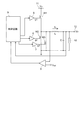
図1は、そのDC−DCコンバータの構成例を示す模式図である。
Hereinafter, embodiments of the present invention will be described with reference to the drawings.
The semiconductor device according to the embodiment of the present invention has a plurality of switching elements and can be used for, for example, a DC-DC converter.
FIG. 1 is a schematic diagram illustrating a configuration example of the DC-DC converter.
このDC−DCコンバータは、ハイサイドスイッチング素子である第1のスイッチング素子M1と、ローサイドスイッチング素子である第2のスイッチング素子M2および第3のスイッチング素子M3と、第1のスイッチング素子M1のゲートを駆動するドライバ5と、第2のスイッチング素子M2のゲートを駆動するドライバ6と、第3のスイッチング素子M3のゲートを駆動するドライバ7と、これらドライバ5〜7を制御する制御回路9と、誘導性負荷であるインダクタLと、コンデンサCと、検出回路8とを備える。
This DC-DC converter includes a first switching element M1 that is a high-side switching element, second and third switching elements M2 and M3 that are low-side switching elements, and gates of the first switching element M1. A
このDC−DCコンバータは、ハイサイドスイッチング素子とローサイドスイッチング素子とを交互にオンオフすることで、入力電圧Vinよりも低い(平均)出力電圧Voを負荷10に出力する降圧型DC−DCコンバータ(buck converter)である。
The DC-DC converter is a step-down DC-DC converter (buck) that outputs an output voltage Vo (average) lower than the input voltage Vin to the
図1に示す要素において、第1のスイッチング素子M1、第2のスイッチング素子M2、第3のスイッチング素子M3、ドライバ5〜7、制御回路9、検出回路8は、1チップ(もしくは1パッケージ)化された電源ICとして構成される。
In the elements shown in FIG. 1, the first switching element M1, the second switching element M2, the third switching element M3, the
スイッチング素子M1、M2、M3は、MOSFET(Metal-Oxide-Semiconductor Field Effect Transistor)であり、それぞれ、ドライバ5、6、7を介して制御回路9から供給されるゲート駆動信号g1、g2、g3によってオンオフされる。
The switching elements M1, M2, and M3 are MOSFETs (Metal-Oxide-Semiconductor Field Effect Transistors), which are respectively supplied by gate drive signals g1, g2, and g3 supplied from the
入力電圧Vinが与えられる入力電圧ライン11と出力端子12との間に、第1のスイッチング素子M1とインダクタLが直列に接続されている。第1のスイッチング素子M1は、例えばP型MOSFETであり、そのソース端子が基準電圧ライン11に接続され、ドレイン端子がインダクタLに接続される。
The first switching element M1 and the inductor L are connected in series between the
第1のスイッチング素子M1とインダクタLとの接続点と、基準電圧ライン(例えばグランドライン)との間に、第2のスイッチング素子M2及び第3のスイッチング素子M3が並列に接続されている。 A second switching element M2 and a third switching element M3 are connected in parallel between a connection point between the first switching element M1 and the inductor L and a reference voltage line (for example, a ground line).
第2のスイッチング素子M2及び第3のスイッチング素子M3は、例えばN型MOSFETであり、各々のドレイン端子は第1のスイッチング素子M1のドレイン端子及びインダクタLに接続され、各々のソース端子はグランドラインに接続されている。 The second switching element M2 and the third switching element M3 are, for example, N-type MOSFETs, each drain terminal is connected to the drain terminal of the first switching element M1 and the inductor L, and each source terminal is a ground line. It is connected to the.
インダクタLと出力端子12との接続点は、出力電圧を短時間に大きく変動させないための平滑コンデンサCを介して接地されている。
A connection point between the inductor L and the
また、ローサイドスイッチング素子(第2のスイッチング素子M2及び第3のスイッチング素子M3)と、インダクタLとの接続点の電位を検出する検出回路8が設けられている。具体的に、検出回路8は、ローサイドスイッチング素子とインダクタLとの接続点の電位をリファレンス電位Vrefと比較するコンパレータである。
In addition, a
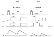
図7(a)は、図1に示すDC−DCコンバータにおける、軽負荷時でない通常動作時の前記ゲート駆動信号g1〜g3およびインダクタ電流ILの波形図である。ILは、正のときはインダクタLから負荷10に向けて流れ、負のときはインダクタLからローサイドスイッチング素子を介してグランドに流れる。
FIG. 7A is a waveform diagram of the gate drive signals g1 to g3 and the inductor current IL during normal operation that is not under light load in the DC-DC converter shown in FIG. IL flows from the inductor L toward the
第1のスイッチング素子M1のゲート端子と第2のスイッチング素子M2のゲート端子には、ほぼ反転位相のゲート駆動信号g1、g2が供給される。第3のスイッチング素子M3は、第2のスイッチング素子M2と同じタイミングでオンオフされる。あるいは、通常動作時、第3のスイッチング素子M3は常時オフであってもよい。 Gate drive signals g1 and g2 having substantially inverted phases are supplied to the gate terminal of the first switching element M1 and the gate terminal of the second switching element M2. The third switching element M3 is turned on / off at the same timing as the second switching element M2. Alternatively, the third switching element M3 may be always off during normal operation.
第1のスイッチング素子M1がオンで、第2のスイッチング素子M2及び第3のスイッチング素子M3がオフのときは、入力電圧ライン11から第1のスイッチング素子M1及びインダクタLを経由して負荷10に電流が供給される。このとき、インダクタ電流ILは増加し、インダクタLにエネルギーが蓄積される。
When the first switching element M1 is on and the second switching element M2 and the third switching element M3 are off, the
そして、第1のスイッチング素子M1がオフに、第2のスイッチング素子M2がオンになると、インダクタLは蓄積したエネルギーを放出し、グランドから第2のスイッチング素子M2及びインダクタLを経由して負荷10に電流が供給される。このとき第3のスイッチング素子M3はオフであってもよい。これは、後述するように、第3のスイッチング素子M3がMOSFETとして動作するときの電流駆動能力は第2のスイッチング素子M2に比べて十分小さいので、ほとんど第2のスイッチング素子M2の電気的特性でコンバータの特性が決定するためである。
When the first switching element M1 is turned off and the second switching element M2 is turned on, the inductor L releases the accumulated energy, and the
また、出力電圧Voは監視され、所定の目標電圧となるように、制御回路9によって第1のスイッチング素子M1及び第2のスイッチング素子M2のオンオフデューティが制御される。
The output voltage Vo is monitored, and the on / off duty of the first switching element M1 and the second switching element M2 is controlled by the
また、第1のスイッチング素子M1と第2のスイッチング素子M2とが同時にオンにされると、非常に大きな電流(貫通電流)が入力電圧ライン11からスイッチング素子M1、M2を介してグランドに流れることになる。これを避けるために、スイッチング素子M1、M2のオンオフのデューティを設定するにあたって、両スイッチング素子M1、M2が共にオフとなる期間であるデッドタイムを設定している。同じ理由から、第1のスイッチング素子M1と第3のスイッチング素子M3も同時にオンにならないようにデッドタイムが設定される。
Further, when the first switching element M1 and the second switching element M2 are simultaneously turned on, a very large current (through current) flows from the
次に、第2のスイッチング素子M2と第3のスイッチング素子M3の具体的な構造について説明する。以下の具体例では、半導体材料として例えばシリコンを用いた例を説明するが、シリコンに限らず他の半導体材料も使用可能である。また、第1導電型をP型、第2導電型をN型として説明するが、第1導電型がN型、第2導電型がP型であってもよい。 Next, specific structures of the second switching element M2 and the third switching element M3 will be described. In the following specific example, an example in which silicon is used as a semiconductor material will be described. However, not only silicon but also other semiconductor materials can be used. Although the first conductivity type is described as P type and the second conductivity type is described as N type, the first conductivity type may be N type and the second conductivity type may be P type.
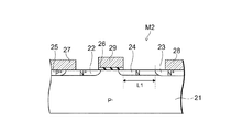
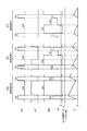
図2は、第2のスイッチング素子M2の要部断面構造を示す模式図である。 FIG. 2 is a schematic diagram illustrating a cross-sectional structure of a main part of the second switching element M2.
第2のスイッチング素子M2は、P−型層21の表層部に、P+型のコンタクト層25、N+型のソース層22、N型のドリフト層24、N+型のドレイン層23が形成され、さらにそれら表面上に第1の主電極28、第2の主電極27、ゲート電極29が設けられたLDMOS(Lateral Diffusion Metal-Oxide-Semiconductor)構造を有する。
In the second switching element M2, a P + -
ソース層22とドレイン層23とは互いに離間して設けられ、これらの間にはドリフト層24がドレイン層23に接して設けられている。ドリフト層24は、ソース層22及びドレイン層23よりも不純物濃度が低い。
The
ソース層22とドリフト層24との間のP−型層21表面上にはゲート絶縁膜26を介してゲート電極29が設けられている。ソース層22における、ゲート電極29側とは反対側の端部には、P−型層21よりも不純物濃度が高いP+型のコンタクト層25がソース層22に接して設けられている。
A
ソース層22とコンタクト層25の表面上にはソース電極として機能する第2の主電極27が設けられている。これにより、ソース層22は第2の主電極27と電気的に接続され、P−型層21はコンタクト層25を介してソース電位とされる。ドレイン層23の表面上にはドレイン電極として機能する第1の主電極28が設けられ、ドレイン層23は第1の主電極28と電気的に接続されている。
A second
ゲート電極29に所定のゲート電圧が与えられると、ゲート電極29下のP−型層21表層部にN型の反転層(チャネル)が形成され、ドレイン層23、ドリフト層24、チャネルおよびソース層22を介して、第1の主電極28と第2の主電極27との間にドレイン電流が流れる。
When a predetermined gate voltage is applied to the
DC−DCコンバータに使用されるスイッチング素子は低オン抵抗と高速性が求められる。特に高速性を実現するためには、ゲート−ドレイン間の容量を減らすことが重要である。 A switching element used in a DC-DC converter is required to have low on-resistance and high speed. In particular, to achieve high speed, it is important to reduce the gate-drain capacitance.
図2に示す構造の場合、ゲート電極29をマスクとしてドリフト層24をセルフアラインすることで、ゲート−ドレイン間容量が極力小さくなるようにされている。すなわち、ドリフト層24は、ゲート電極29形成後にイオン注入にてP−型層21表層部にN型不純物を注入することによって形成される。通常、ゲート電極形成後は、ハイサイドスイッチング素子及びローサイドスイッチング素子と共に混載されるドライバ等を構成するCMOS等に影響を与えるため、熱処理工程はほとんどない。したがって、P−型層21中へのドリフト層24の接合深さ(N型不純物拡散深さ)は浅い。
In the structure shown in FIG. 2, the gate-drain capacitance is made as small as possible by self-aligning the drift layer 24 using the
再び図1を参照すると、ローサイドスイッチング素子(第2のスイッチング素子M2、第3のスイッチング素子M3)のドレイン端子は、これらを集積回路として形成したICに対して外部部品となるインダクタLに接続するための外部端子となる。そのため、ESD(Electro Static Discharge)にさらされることが起こり得、その外部端子にサージ(瞬間的に発生する過剰電圧、電流パルスなどの電気的ストレス)が印加しても破壊されないことがICには求められる。 Referring to FIG. 1 again, the drain terminals of the low-side switching elements (second switching element M2 and third switching element M3) are connected to an inductor L which is an external component for an IC formed as an integrated circuit. For external terminals. For this reason, the IC can be exposed to ESD (Electro Static Discharge), and it is not destroyed even if a surge (electrical stress such as instantaneously generated excessive voltage or current pulse) is applied to the external terminal. Desired.
図2に示す構造において、ドレイン端子にESDサージが印加されると、ゲート−ドレイン間の電界が強くなり、大きなアバランシェ電流が流れる。前述したようにドリフト層24の接合深さは浅いため、ドリフト層24に電流が集中し、信頼性が低下する問題が懸念される。 In the structure shown in FIG. 2, when an ESD surge is applied to the drain terminal, the electric field between the gate and the drain becomes strong, and a large avalanche current flows. As described above, since the junction depth of the drift layer 24 is shallow, there is a concern that current concentrates on the drift layer 24 and reliability is lowered.
そこで、本実施形態では、ESD保護素子としての機能を有する第3のスイッチング素子M3を第2のスイッチング素子M2に対して並列に設けている。
図3は、その第3のスイッチング素子M3の要部断面構造を示す模式図である。
Therefore, in the present embodiment, the third switching element M3 having a function as an ESD protection element is provided in parallel to the second switching element M2.
FIG. 3 is a schematic diagram showing a cross-sectional structure of a main part of the third switching element M3.
第3スイッチング素子M3も、第2のスイッチング素子M2と同様、P−型層21の表層部に、P+型のコンタクト層37、N+型のソース層32、N型のドリフト層34、N+型のドレイン層33が形成され、さらにそれら表面上に第1の主電極28、第2の主電極27、ゲート電極29が設けられたLDMOS構造を有する。
The third switching device M3 is also similar to the second switching element M2, P - the surface portion of the
ソース層32とドレイン層33とは互いに離間して設けられ、これらの間にはドリフト層34がドレイン層33に接して設けられている。ドリフト層34は、ソース層32及びドレイン層33よりも不純物濃度が低い。
The
ソース層32とドリフト層34との間のP−型層21表面上にはゲート絶縁膜26を介してゲート電極29が設けられている。ソース層32における、ゲート電極29側とは反対側の端部には、P−型層21よりも不純物濃度が高いP+型のコンタクト層37がソース層32に接して設けられている。
A
さらに、第3のスイッチング素子M3において、P+型のアノード層36がドレイン層33中に設けられ、またドレイン層33及びアノード層36の下に、これらに接してN型層31が設けられている。
Further, in the third switching element M3, a P + -
ソース層32とコンタクト層37の表面上には第2の主電極27が設けられている。これにより、ソース層32は第2の主電極27と電気的に接続され、P−型層21はコンタクト層37を介してソース電位とされる。ドレイン層33及びアノード層36の表面上には第1の主電極28が設けられ、ドレイン層33及びアノード層36は第1の主電極28と電気的に接続されている。
A second
第3のスイッチング素子M3において、アノード層36とN型層31とP−型層21はPNP型のバイポーラトランジスタを構成し、コンタクト層37とP−型層21とN型層31はNPN型のバイポーラトランジスタを構成し、これらPNP型トランジスタ及びNPN型トランジスタによってサイリスタが構成される。サイリスタ動作するときは、第1の主電極28がアノード電極として機能し、第2の主電極27がカソード電極として機能する。
In the third switching element M3, the
したがって、第3のスイッチング素子M3は、MOS構造部とサイリスタ構造部とが、第1の主電極28と第2の主電極27間に並列に接続された構成を有する。
Therefore, the third switching element M3 has a configuration in which the MOS structure portion and the thyristor structure portion are connected in parallel between the first
ドレイン端子にESDサージが飛び込まず、第1の主電極28と第2の主電極27間にかかる電圧が定格電圧以内のときは、上記サイリスタは動作せず、ゲート電極29に与えられるゲート電圧に応じてMOS構造部がオンオフする。すなわち、ゲート電極29にしきい値電圧以上の電圧が印加されるとゲート電極29下のP−型層21表層部にチャネルが形成され、ドレイン層33、ドリフト層34、チャネルおよびソース層32を介して第1の主電極28と第2の主電極27間に電流が流れる(この電流経路を主電流経路とする)。ゲート電圧がしきい値電圧より低い場合には、ゲート電極29下にチャネルは形成されず、第1の主電極28と第2の主電極27間は導通せず、第3のスイッチング素子M3はオフ状態となる。
When the ESD surge does not jump into the drain terminal and the voltage applied between the first
MOS構造部における上記主電流経路に対して、サイリスタはサージ印加時にサージ電流が流れるサージ電流経路として機能する。 In contrast to the main current path in the MOS structure, the thyristor functions as a surge current path through which a surge current flows when a surge is applied.
第3のスイッチング素子M3のサイリスタはアバランシェブレークダウンをトリガーとして活性化される。そこで、前述した外部端子(ローサイドスイッチング素子のドレイン端子)にサージが飛び込んだときに、第3のスイッチング素子M3でアバランシェブレークダウンが起きるように、第3のスイッチング素子M3は、第2のスイッチング素子M2よりも耐圧が低くなるように設計されている。具体的には、第3のスイッチング素子M3におけるドリフト層34の長さL2が、第2のスイッチング素子M2におけるドリフト層24の長さL1よりも短い(L1>L2)。ここでの、ドリフト層の長さとは、ゲートとドレインとを結ぶ方向の長さを意味する。
The thyristor of the third switching element M3 is activated with avalanche breakdown as a trigger. Therefore, the third switching element M3 is configured so that the avalanche breakdown occurs in the third switching element M3 when a surge jumps into the external terminal (the drain terminal of the low-side switching element) described above. It is designed to have a breakdown voltage lower than M2. Specifically, the length L2 of the
上記外部端子に正のサージ電圧(第2の主電極27に対して第1の主電極28が高電位となるサージ電圧)が印加された場合、ゲート電極29(図示しないプルダウン抵抗を介して第2の主電極27の電位と同電位になっている)と、第1の主電極28との間に高電圧が印加され、ドリフト層は空乏化する。ここで、第3のスイッチング素子M3の方が第2のスイッチング素子M2よりも耐圧が低い(ドリフト層の長さが短い)ことから、第3のスイッチング素子M3のドレイン層33におけるゲート電極29側端部の電界強度がより高くなり、そのポイントでアバランシェブレークダウンを起こす。
When a positive surge voltage (surge voltage at which the first
このアバランシェブレークダウンにより電子と正孔が発生し、正孔はP−型層21とコンタクト層37を通って第2の主電極27に流れ、電子はドレイン層33におけるゲート電極29側の端部からアノード層36下のN型層31をまわり込んで第1の主電極28に流れる。
Electrons and holes are generated by this avalanche breakdown, the holes flow through the P − type layer 21 and the
ここで、電子がN型層31を移動するときN型層31に存在する寄生抵抗によって電圧降下が生じる。すなわち、第1の主電極28にオーミックコンタクトし第1の主電極28と同電位であるアノード層36の電位をVd、N型層31の抵抗をR、N型層31を流れる電流をIとすると、N型層31の電位はアノード層36の電位Vdより低い(Vd−RI)となる。
Here, when electrons move through the N-
したがって、アノード層36とN型層31とのPN接合に順方向のバイアスがかかり、アノード層36から正孔がP−型層21に注入される。これはNPNトランジスタのベース電流となり、これに応じて流れるNPNトランジスタのコレクタ電流がPNPトランジスタのベース電流となり、このベース電流に対応したPNPトランジスタのコレクタ電流がNPNトランジスタのベース電流となるといったサイクルが繰り返され、サイリスタが活性化される。
Therefore, a forward bias is applied to the PN junction between the
サイリスタが活性化することで、サイリスタを介した第1の主電極28と第2の主電極27間の経路が、大電流を流すことが可能な低抵抗状態になる。これにより、より小さな素子面積で、サイリスタを通じて速やかにサージ電流をグランドに放電することができる。すなわち、サージ電圧印加時、第3のスイッチング素子M3が応答性良くサイリスタ動作して速やかにサージ電流を引き込んでグランドへと流すことで、第2のスイッチング素子M2のサージによる破壊を防ぐことができる。
When the thyristor is activated, the path between the first
ESD保護機能を有する第3のスイッチング素子M3を設けず、第2のスイッチング素子M2自体をESD耐量に優れた素子構造とすることも考えられるが、通常、ESD耐量を持たせるには第1の主電極と第2の主電極間の距離が長くなり、コンバータのスイッチング素子として機能するときのオン抵抗が大きくなってしまう。 Although it is conceivable that the third switching element M3 having an ESD protection function is not provided and the second switching element M2 itself has an element structure with excellent ESD tolerance, the first resistance is usually required to have the ESD tolerance. The distance between the main electrode and the second main electrode is increased, and the on-resistance when functioning as a switching element of the converter is increased.
本実施形態では、ESD保護素子としての機能は第3のスイッチング素子M3が担い、DC−DCコンバータにおけるローサイドスイッチング素子としての役割はほとんど第2のスイッチング素子M2が担うため、第2のスイッチング素子M2は、コンバータで必要とされる特性を最優先した設計を行える。すなわち、それぞれ役割を分担した第2のスイッチング素子M2と第3のスイッチング素子M3とからローサイドスイッチング素子を構成することで、DC−DCコンバータ本来の特性は損ねずに、なおかつESDからの保護も実現できる。 In the present embodiment, the third switching element M3 plays a function as an ESD protection element, and the second switching element M2 plays almost the role as a low-side switching element in the DC-DC converter. Can be designed with the highest priority on the characteristics required by the converter. That is, by forming the low-side switching element from the second switching element M2 and the third switching element M3 that share the respective roles, the original characteristics of the DC-DC converter are not impaired, and protection from ESD is also realized. it can.
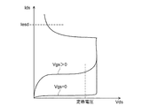
図4は、第3のスイッチング素子M3におけるドレイン−ソース間電圧(第1の主電極28−第2の主電極27間電圧)Vdsと、ドレイン電流Idsとの関係を示す特性図である。縦軸のIesdは、ESDサージ電流の最大電流値である。また、図4にはゲート電圧Vgsがゼロボルトの場合(Vgs=0)と、ゼロボルトより大きい場合(Vgs>0)とを示している。
FIG. 4 is a characteristic diagram showing a relationship between the drain-source voltage (voltage between the first
ドレイン−ソース間電圧Vdsが定格電圧以内では、第3のスイッチング素子M3はサイリスタ動作しないが、定格電圧より大きなESDの高電圧が印加されたときはサイリスタ動作する。すなわち、第3のスイッチング素子M3は、定格電圧以内ではスイッチングMOSFETとして機能し、ESD印加時はESD保護素子として機能する。 When the drain-source voltage Vds is within the rated voltage, the third switching element M3 does not operate as a thyristor, but operates when a high ESD voltage higher than the rated voltage is applied. That is, the third switching element M3 functions as a switching MOSFET within the rated voltage, and functions as an ESD protection element when ESD is applied.
次に、図5は、第3のスイッチング素子M3の他の具体例を示す模式断面図である。 Next, FIG. 5 is a schematic cross-sectional view showing another specific example of the third switching element M3.
図5に示す第3のスイッチング素子M3は次のような構造を有する。P型基板41上に、高不純物濃度のN+型埋め込み層42が設けられ、そのN+型埋め込み層42の上に、N−型層43とP−型層44が選択的に設けられている。N−型層43の上にはP−型層44に隣接してP型ベース層47が設けられている。
The third switching element M3 shown in FIG. 5 has the following structure. A high impurity concentration N + type buried
P型ベース層47の表層部に、N+型のソース層46とP+型のコンタクト層45が選択的に設けられている。ソース層46とコンタクト層45は隣接し、それら表面上に第2の主電極27が設けられている。ソース層46及びコンタクト層45は第2の主電極27と電気的に接続され、またPベース層47にはコンタクト層45を介して第2の主電極27の電位が与えられる。
An N + -
P−型層44の表層部には、N+型のドレイン層49とN型のドリフト層48が選択的に設けられている。ドリフト層48はソース層46とドレイン層49との間に位置し、ドレイン層49に隣接している。ドリフト層48はドレイン層49よりも不純物濃度が低く、例えばドリフト層48の不純物濃度は2×10¹²〜4×10¹²/cm2である。
On the surface layer portion of the P − type layer 44, an N +
ソース層46とドリフト層48との間におけるP型ベース層47及びP−型層44の表面上には、ゲート絶縁膜26を介してゲート電極29が設けられている。
A
ドレイン層49側のN+型埋め込み層42の上には素子表面に至るまでN+型層51が設けられている。ドレイン層49とN+型層51とは抵抗を介して接続され、また、ドレイン層49及びN+型層51は第1の主電極28と電気的に接続されている。
On the N + type buried
この図5に示す第3のスイッチング素子M3において、ドレイン層49、ドリフト層48、ゲート電極29、P型ベース層47及びP−型層44におけるゲート電極29下のチャネル形成領域、ソース層46はLDMOSを構成する。また、ソース層46、P型ベース層47、N−型層43、N+型埋め込み層42、N+型層51はNPN型のバイポーラトランジスタTr1を構成する。これらLDMOSとバイポーラトランジスタTr1は、第1の主電極28と第2の主電極27間に並列に接続されている。バイポーラトランジスタTr1はサージ印加時にサージ電流が流れるサージ電流経路として機能する。
In the third switching element M3 shown in FIG. 5, the
バイポーラトランジスタTr1はアバランシェブレークダウンをトリガーとして活性化される。そこで、前述した外部端子(ローサイドスイッチング素子のドレイン端子)にサージが飛び込んだときに、第3のスイッチング素子M3でアバランシェブレークダウンが起きるように、第3のスイッチング素子M3は、第2のスイッチング素子M2よりも耐圧が低くなるように設計されている。すなわち、図5に示す第3のスイッチング素子M3においても、そのドリフト層48の長さL2は、図2に示す第2のスイッチング素子M2のドリフト層24の長さL1よりも短い(L1>L2)。
The bipolar transistor Tr1 is activated with avalanche breakdown as a trigger. Therefore, the third switching element M3 is configured so that the avalanche breakdown occurs in the third switching element M3 when a surge jumps into the external terminal (the drain terminal of the low-side switching element) described above. It is designed to have a breakdown voltage lower than M2. That is, also in the third switching element M3 shown in FIG. 5, the length L2 of the
上記外部端子に正のサージ電圧が印加された場合、図示しないプルダウン抵抗を介して第2の主電極27の電位と同電位になっているゲート電極29と、第1の主電極28との間に高電圧が印加され、ドリフト層は空乏化する。ここで、第3のスイッチング素子M3の方が第2のスイッチング素子M2よりも耐圧が低い(ドリフト層の長さが短い)ことから、第3のスイッチング素子M3のドレイン層49におけるゲート電極29側端部の電界強度がより高くなり、そのポイントでアバランシェブレークダウンを起こす。
When a positive surge voltage is applied to the external terminal, between the first
このアバランシェブレークダウンにより電子と正孔が発生し、電子は第1の主電極28に流れ、正孔はP−型層44、P型ベース層47、コンタクト層45を通って第2の主電極27に流れる。
Electrons and holes are generated by this avalanche breakdown, the electrons flow to the first
ここで、正孔がP型ベース層47を移動するときP型ベース層47に存在する寄生抵抗によって電圧降下が生じる。すなわち、第2の主電極27にオーミックコンタクトし第2の主電極27と同電位であるソース層46の電位をVs、P型ベース層47の抵抗をR、P型ベース層47を流れる電流をIとすると、P型ベース層47におけるソース層46下の電位はVsより低い(Vs−RI)となる。
Here, when holes move in the P-
したがって、ソース層46とP型ベース層47とのPN接合に順方向のバイアスがかかり、ソース層46から電子がN−型層43及びN+型埋め込み層42に注入される。これにより、NPN型バイポーラトランジスタTrが活性化される。
Therefore, a forward bias is applied to the PN junction between the
バイポーラトランジスタTr1が活性化することで、そのバイポーラトランジスタTr1を通じた第1の主電極28と第2の主電極27間の経路が、大電流を流すことが可能な低抵抗状態になる。これにより、より小さな素子面積で、バイポーラトランジスタTr1を通じて速やかにサージ電流をグランドに放電することができる。すなわち、サージ電圧印加時、第3のスイッチング素子M3が応答性良くサイリスタ動作して速やかにサージ電流を引き込んでグランドへと流すことで、第2のスイッチング素子M2のサージによる破壊を防ぐことができる。
When the bipolar transistor Tr1 is activated, the path between the first
上記外部端子に負のサージ電圧(第2の主電極27に対して第1の主電極28が低電位となるサージ電圧)が印加された場合、コンタクト層45、P型ベース層47、P−型層44、N+型埋め込み層42、N+型層51、ドレイン層49から構成されるPNダイオードに順方向バイアスがかかり、そのダイオードを通じてサージ電流は速やかにグランドへと流れる。
When a negative surge voltage (surge voltage at which the first
ESDサージが飛び込まず、第1の主電極28と第2の主電極27間にかかる電圧が定格電圧以内のときは、上記バイポーラトランジスタTr1は動作せず、ゲート電極29に与えられるゲート電圧に応じてLDMOSがオンオフする。
When the ESD surge does not jump in and the voltage applied between the first
すなわち、ゲート電極29にしきい値電圧以上の電圧が印加されるとゲート電極29下のP型ベース層47及びP−型層44表層部にチャネルが形成され、ドレイン層49、ドリフト層48、チャネルおよびソース層46を介して第1の主電極28と第2の主電極27間に電流が流れる。ゲート電圧がしきい値電圧より低い場合には、ゲート電極29下にチャネルは形成されず、第1の主電極28と第2の主電極27間は導通せず、第3のスイッチング素子M3はオフ状態となる。
That is, when a voltage equal to or higher than the threshold voltage is applied to the
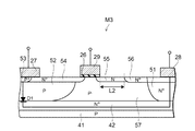
次に、図6は、第3のスイッチング素子M3のさらに他の具体例を示す模式断面図である。 Next, FIG. 6 is a schematic cross-sectional view showing still another specific example of the third switching element M3.
図6に示す第3のスイッチング素子M3は次のような構造を有する。P型基板41上に、高不純物濃度のN+型埋め込み層42が設けられ、そのN+型埋め込み層42の上に、P型層52とP−型層57とが隣接して設けられている。
The third switching element M3 shown in FIG. 6 has the following structure. A high impurity concentration N + type buried
P型層52及びP−型層57の表層部に、N+型のソース層54が選択的に設けられている。また、P型層52の表層部に、ソース層54に隣接してP+型のコンタクト層53が設けられている。
An N + -
ソース層54及びコンタクト層53の表面上に第2の主電極27が設けられ、ソース層54及びコンタクト層53は第2の主電極27と電気的に接続されている。またP型層52にはコンタクト層53を介して第2の主電極27の電位が与えられる。
A second
P−型層57の表層部には、N+型のドレイン層56とN型のドリフト層55が選択的に設けられている。ドリフト層55はソース層54とドレイン層56との間に位置し、ドレイン層56に隣接している。ドリフト層55はドレイン層56よりも不純物濃度が低く、例えばドリフト層55の不純物濃度は2×10¹²〜4×10¹²/cm2である。
On the surface layer portion of the P − type layer 57, an N +
ソース層54とドリフト層55との間におけるP−型層57の表面上には、ゲート絶縁膜26を介してゲート電極29が設けられている。
On the surface of the P − -
ドレイン層56下のN+型埋め込み層42の上には、ドレイン層56に接してN+型層51が設けられている。ドレイン層56及びN+型層51は第1の主電極28と電気的に接続されている。
On the N + type buried
この図6に示す第3のスイッチング素子M3において、ドレイン層56、ドリフト層55、ゲート電極29、P−型層57におけるゲート電極29下のチャネル形成領域、ソース層54はLDMOSを構成する。また、コンタクト層53、P型層52、N+型埋め込み層42、N+型層51はPNダイオードD1を構成する。これらLDMOSとダイオードD1は、第1の主電極28と第2の主電極27間に並列に接続されている。ダイオードD1はサージ印加時にサージ電流が流れるサージ電流経路として機能する。
In the third switching element M3 shown in FIG. 6, the
前述した外部端子(ローサイドスイッチング素子のドレイン端子)にサージが飛び込んだときに、第3のスイッチング素子M3の上記ダイオードD1でなだれ降伏が起きるように、第3のスイッチング素子M3は、第2のスイッチング素子M2よりも耐圧が低く設計されている。 The third switching element M3 is connected to the second switching element so that the avalanche breakdown occurs in the diode D1 of the third switching element M3 when a surge enters the external terminal (the drain terminal of the low-side switching element). The breakdown voltage is designed to be lower than that of the element M2.
また、第3のスイッチング素子M3において、LDMOSにおける第1の主電極28とゲート電極29間の耐圧は、ダイオードD1の耐圧よりも大きく設定されている。このような耐圧関係は、ドリフト層55の長さL2を長くする、P型層52の拡散深さを深くする、P型層52の不純物濃度を高くすることなどによってコントロール可能である。
In the third switching element M3, the breakdown voltage between the first
前述した外部端子に正のサージ電圧(ダイオードD1にとっては逆方向バイアス)が印加された場合、ダイオードD1がなだれ降伏する。このなだれ降伏する箇所はP型層52とN+型埋め込み層42との接合面であり、比較的広い面全体にわたって電界集中箇所が形成されるため電流集中が起きにくく、ダイオードD1は破壊に強い電気的特性を有する。上記なだれ降伏により、ダイオードD1を通じた第1の主電極28と第2の主電極27間の経路が、大電流を流すことが可能な低抵抗状態になり、サージ電流を速やかにグランドへと流すことができる。
When a positive surge voltage (reverse bias for the diode D1) is applied to the external terminal described above, the diode D1 avalanche breaks down. The avalanche breakdown location is the junction surface between the P-
上記外部端子に負のサージ電圧が印加された場合、ダイオードD1にとって順方向バイアスであるため、そのダイオードD1を通じてサージ電流は速やかにグランドへと流れる。 When a negative surge voltage is applied to the external terminal, since the diode D1 is forward biased, the surge current quickly flows to the ground through the diode D1.
ESDサージが飛び込まず、第1の主電極28と第2の主電極27間にかかる電圧が定格電圧以内のときは、上記ダイオードD1は動作せず、ゲート電極29に与えられるゲート電圧に応じてLDMOSがオンオフする。
When the ESD surge does not jump in and the voltage applied between the first
すなわち、ゲート電極29にしきい値電圧以上の電圧が印加されるとゲート電極29下のP−型層57表層部にチャネルが形成され、ドレイン層56、ドリフト層55、チャネルおよびソース層54を介して第1の主電極28と第2の主電極27間に電流が流れる。ゲート電圧がしきい値電圧より低い場合には、ゲート電極29下にチャネルは形成されず、第1の主電極28と第2の主電極27間は導通せず、第3のスイッチング素子M3はオフ状態となる。
That is, when a voltage equal to or higher than the threshold voltage is applied to the
次に、第2のスイッチング素子M2と第3のスイッチング素子M3の、オンオフのタイミングについて説明する。 Next, the on / off timing of the second switching element M2 and the third switching element M3 will be described.
通常動作時、図7(a)に示すように、第3のスイッチング素子M3は第2のスイッチング素子M2と同じタイミングでオンする。これらローサイドスイッチング素子がオンのとき、第2のスイッチング素子M2及び第3のスイッチング素子M3はインダクタLを介して負荷10に電流を供給する。ただし、第3のスイッチング素子M3は常時オフでもコンバータの特性には大きく影響しない。これは、後述するように第3のスイッチング素子M3の電流駆動能力は第2のスイッチング素子M2に比べて十分小さいので、ほとんど第2のスイッチング素子M2の電気的特性でコンバータの特性を決定しているためである。
During normal operation, as shown in FIG. 7A, the third switching element M3 is turned on at the same timing as the second switching element M2. When these low-side switching elements are on, the second switching element M2 and the third switching element M3 supply current to the
ハイサイドスイッチング素子(第1のスイッチング素子M1)がオンで、ローサイドスイッチング素子(第2のスイッチング素子M2及び第3のスイッチング素子M3)がオフである期間、負荷10に向かって流れる方向の(正の)インダクタ電流ILは増大していき、インダクタLにエネルギーが蓄積される。 In a period in which the high-side switching element (first switching element M1) is on and the low-side switching elements (second switching element M2 and third switching element M3) are off (positive) Inductor current IL increases and energy is stored in inductor L.
しかし、負荷10に流れる電流が小さな軽負荷時において、インダクタLに流れる電流値が小さいと、ハイサイドスイッチング素子(第1のスイッチング素子M1)のオン時にインダクタLに蓄積されるエネルギーが小さい。そのため、ローサイドスイッチング素子がオンとなっている期間中、あるタイミングでインダクタLに蓄積されたエネルギーがゼロとなる。その後、インダクタLに流れる電流は負荷10からローサイドスイッチング素子を介してグランドに流れる。この電流は負荷10に供給されるものではないため無効電流となり電力の変換効率(出力電力/入力電力×100%)を大幅に低下させる。
However, if the current value flowing through the inductor L is small when the current flowing through the
特に、携帯機器等のバッテリー駆動の機器では、軽負荷時においてもDC−DCコンバータの変換効率が優れていることが求められている。 In particular, battery-driven devices such as portable devices are required to have excellent conversion efficiency of the DC-DC converter even at light loads.
そこで、本実施形態では、第2のスイッチング素子M2については所望のコンバータ特性を得るのに必要な電流駆動能力を有するようにし、これに対して第3のスイッチング素子M3については第2のスイッチング素子M2よりも十分低い電流駆動能力となるようにしている。なお、ここでの電流駆動能力は、ESDサージ印加時ではなく、定格電圧以内でMOSFETとして動作する時の電流駆動能力である。第3のスイッチング素子M3の方が第2のスイッチング素子M2よりも電流駆動能力が低いということは、第3のスイッチング素子M3の方が第2のスイッチング素子M2よりもオン抵抗が大きい。 Therefore, in the present embodiment, the second switching element M2 has a current driving capability necessary to obtain desired converter characteristics, while the third switching element M3 has the second switching element. The current driving capability is sufficiently lower than M2. Note that the current driving capability here is not the time of ESD surge application but the current driving capability when operating as a MOSFET within the rated voltage. The fact that the third switching element M3 has a lower current drive capability than the second switching element M2 means that the third switching element M3 has a higher on-resistance than the second switching element M2.
例えば、第3のスイッチング素子M3のセル面積を第2のスイッチング素子M2のセル面積よりも小さくする、あるいは第3のスイッチング素子M3の方が第2のスイッチング素子M2よりもしきい値電圧を高く設定することなどで、第2のスイッチング素子M2に比べて第3のスイッチング素子M3の電流駆動能力を低くすることができる。 For example, the cell area of the third switching element M3 is made smaller than the cell area of the second switching element M2, or the threshold voltage of the third switching element M3 is set higher than that of the second switching element M2. By doing so, the current driving capability of the third switching element M3 can be made lower than that of the second switching element M2.
また、本実施形態のDC−DCコンバータは、図1を参照して前述したように、ローサイドスイッチング素子(第2のスイッチング素子M2及び第3のスイッチング素子M3)と、インダクタLとの接続点の電位を監視する検出回路8を有している。検出回路8は、上記接続点の電位を検出してリファレンス電位Vrefと比較する。
Further, as described above with reference to FIG. 1, the DC-DC converter of the present embodiment has a connection point between the low-side switching element (the second switching element M2 and the third switching element M3) and the inductor L. It has a
軽負荷時でない通常動作時において、ハイサイドスイッチング素子がオフで、ローサイドスイッチング素子がオンの期間、グランドからローサイドスイッチング素子を介して上記接続点に電流が流れるので上記接続点の電位は負電位となる。 During normal operation that is not under light load, when the high-side switching element is off and the low-side switching element is on, current flows from the ground to the connection point via the low-side switching element, so the potential at the connection point is a negative potential. Become.
軽負荷時において、ハイサイドスイッチング素子がオフで、ローサイドスイッチング素子がオンの期間中、インダクタに蓄積されるエネルギーがゼロになり、負荷10からインダクタL及びローサイドスイッチング素子を介してグランドに電流が流れると、上記接続点の電位は正電位となる。
During a light load, the energy stored in the inductor becomes zero during the period when the high-side switching element is off and the low-side switching element is on, and current flows from the
したがって、上記接続点の電位とリファレンス電位Vrefとの比較結果から、インダクタ電流ILの正負がわかる。そして、本実施形態では、軽負荷時のタイミングチャートを示す図7(b)に示すように、インダクタ電流ILが負となる期間中、第2のスイッチング素子M2がオフで、第3のスイッチング素子M3がオンとなる期間を設けている。 Therefore, the sign of the inductor current IL can be determined from the comparison result between the potential at the connection point and the reference potential Vref. In the present embodiment, as shown in FIG. 7B showing a timing chart at light load, the second switching element M2 is off during the period in which the inductor current IL is negative, and the third switching element. A period during which M3 is on is provided.
第3のスイッチング素子M3は前述したように電流駆動能力が低い(オン抵抗が大きい)ため、インダクタ電流ILが負となっているときに第3のスイッチング素子M3のみがオン状態になることで、インダクタLからローサイドスイッチング素子を介してグランドに流れる電流を小さく抑えることができる。すなわち、負荷10には供給されずにグランドへと流れる無効電流が減り、効率の低下を抑えることができる。
As described above, since the third switching element M3 has low current drive capability (high on-resistance), only the third switching element M3 is turned on when the inductor current IL is negative. The current flowing from the inductor L to the ground via the low-side switching element can be reduced. That is, the reactive current that flows to the ground without being supplied to the
図7(b)に示すタイミング例では、第2のスイッチング素子M2と第3のスイッチング素子M3が同時にオンする期間があるが、図8に示すように、第2のスイッチング素子M2がオンのときは第3のスイッチング素子M3がオフに、第3のスイッチング素子M3がオンのときは第2のスイッチング素子M2はオフに、というように第2のスイッチング素子M2と第3のスイッチング素子M3とが同時にオンする期間が存在しなくてもよい。これは、第3のスイッチング素子M3の電流駆動能力は第2のスイッチング素子M2に比べて十分小さいので、第2のスイッチング素子M2と第3のスイッチング素子M3とが同時にオンしていても、ほとんど第2のスイッチング素子M2の電気的特性でコンバータの特性が決まるためである。 In the timing example shown in FIG. 7B, there is a period in which the second switching element M2 and the third switching element M3 are simultaneously turned on. However, as shown in FIG. 8, when the second switching element M2 is turned on. When the third switching element M3 is off, the second switching element M2 is off when the third switching element M3 is on, and so on. There may be no period during which the signals are simultaneously turned on. This is because the current driving capability of the third switching element M3 is sufficiently smaller than that of the second switching element M2, so that even if the second switching element M2 and the third switching element M3 are turned on at the same time, This is because the converter characteristics are determined by the electrical characteristics of the second switching element M2.
図7(b)、図8に示す例では、第2のスイッチング素子M2がオフで第3のスイッチング素子M3がオンである期間の開始タイミングはインダクタ電流ILが正からゼロになる直前となっているが、ゼロになった瞬時もしくはゼロになった直後であってもよい。なお、第3のスイッチング素子M3についても第1のスイッチング素子M1と同時にオンとなる期間があると入力電圧ライン11からグランドへと貫通電流が流れてしまうため、第3のスイッチング素子M3は、第1のスイッチング素子M1がオンになるよりも前にオフさせる必要がある。
In the example shown in FIGS. 7B and 8, the start timing of the period in which the second switching element M2 is off and the third switching element M3 is on is immediately before the inductor current IL changes from positive to zero. However, it may be the moment when it becomes zero or immediately after it becomes zero. Note that if the third switching element M3 is also turned on simultaneously with the first switching element M1, a through current flows from the
なお、さらなる軽負荷時においては、ハイサイドスイッチング素子とローサイドスイッチング素子とのスイッチング周波数を小さくすることで効率を改善することができる。 Note that, when the load is further light, the efficiency can be improved by reducing the switching frequency of the high-side switching element and the low-side switching element.
次に、図9は、本発明の他の実施形態に係る半導体装置を用いたDC−DCコンバータの構成例を示す模式図である。
図10は、図9に示すDC−DCコンバータにおけるスイッチング素子M1、M2、M4の動作タイミングおよびインダクタ電流ILの波形を示す。
Next, FIG. 9 is a schematic diagram showing a configuration example of a DC-DC converter using a semiconductor device according to another embodiment of the present invention.
FIG. 10 shows the operation timing of the switching elements M1, M2, and M4 and the waveform of the inductor current IL in the DC-DC converter shown in FIG.
第1のスイッチング素子M1、第2のスイッチング素子M2および第3のスイッチング素子M4はMOSFETである。図1を参照して前述した実施形態と同様、第1のスイッチング素子M1と第2のスイッチング素子M2は、それぞれドライバ5、6を介して制御回路9から供給されるゲート駆動信号g1、g2によってオンオフされる。しかし、本実施形態では、第3のスイッチング素子M4のゲートは常にグランドに接続されている点が図1に示す実施形態と異なる。したがって、第3のスイッチング素子M4のゲート電極とソース電極とが電気的に短絡されている。
The first switching element M1, the second switching element M2, and the third switching element M4 are MOSFETs. As in the embodiment described above with reference to FIG. 1, the first switching element M1 and the second switching element M2 are driven by gate drive signals g1 and g2 supplied from the
第3のスイッチング素子M4は第2のスイッチング素子M2と共に、DC−DCコンバータにおけるローサイドスイッチング素子として機能するが、前述した実施形態における第3のスイッチング素子M3と異なり、必ずしもESD保護機能は備えていなくてもよい。 The third switching element M4 functions as a low-side switching element in the DC-DC converter together with the second switching element M2. However, unlike the third switching element M3 in the above-described embodiment, the third switching element M4 does not necessarily have an ESD protection function. May be.
また、図9には、第2のスイッチング素子M2、第3のスイッチング素子M4におけるそれぞれの内蔵ダイオード(寄生ダイオード)d1、d2を示す。内蔵ダイオードd1、d2は、第2のスイッチング素子M2、第3のスイッチング素子M4のそれぞれのドレイン−ソース間に主電流経路に対して並列に存在し、ソースからドレインに向かう方向を順方向としている。 FIG. 9 shows the internal diodes (parasitic diodes) d1 and d2 in the second switching element M2 and the third switching element M4. The built-in diodes d1 and d2 exist in parallel to the main current path between the drains and the sources of the second switching element M2 and the third switching element M4, and the direction from the source to the drain is the forward direction. .
第2のスイッチング素子M2のサイズは第3のスイッチング素子M4のサイズよりも大きい。
また、第3のスイッチング素子M4の閾値電圧は次のように設定されている。
0<(第3のスイッチング素子M4の閾値電圧)<(第2のスイッチング素子M2の内蔵ダイオードd1のオン電圧)…(1)。
The size of the second switching element M2 is larger than the size of the third switching element M4.
The threshold voltage of the third switching element M4 is set as follows.
0 <(threshold voltage of the third switching element M4) <(ON voltage of the built-in diode d1 of the second switching element M2) (1).
こうすることで、第1のスイッチング素子M1と第2のスイッチング素子M2との接続点の電位が、−(第3のスイッチング素子M4の閾値電圧)より大きくなると第3のスイッチング素子M4はオフし、上記接続点の電位が、−(第3のスイッチング素子M4の閾値電圧)より小さくなると第3のスイッチング素子M3はオンする。 As a result, when the potential at the connection point between the first switching element M1 and the second switching element M2 becomes higher than − (threshold voltage of the third switching element M4), the third switching element M4 is turned off. When the potential at the connection point becomes smaller than − (threshold voltage of the third switching element M4), the third switching element M3 is turned on.
図10(a)に示す通常動作時において、第1のスイッチング素子M1がオフの期間は、第1のスイッチング素子M1と第2のスイッチング素子M2との接続点の電位は負になる。第1のスイッチング素子M1と第2のスイッチング素子M2が両方ともオフの期間は、もし第3のスイッチング素子M4がない場合には、第1のスイッチング素子M1と第2のスイッチング素子M2との接続点の電位は、−(第2のスイッチング素子M2の内蔵ダイオードd1のオン電圧)となる。しかし、第3のスイッチング素子M4が存在することで、第3のスイッチング素子M4のゲート−ソース間電圧が上記(1)式の関係より閾値電圧以上となり、第3のスイッチング素子M4はオン状態となる。 In the normal operation shown in FIG. 10A, the potential at the connection point between the first switching element M1 and the second switching element M2 is negative during the period in which the first switching element M1 is off. During the period when both the first switching element M1 and the second switching element M2 are off, if there is no third switching element M4, the connection between the first switching element M1 and the second switching element M2 The potential at the point becomes − (on voltage of the built-in diode d1 of the second switching element M2). However, due to the presence of the third switching element M4, the gate-source voltage of the third switching element M4 becomes equal to or higher than the threshold voltage according to the relationship of the above expression (1), and the third switching element M4 is in the on state. Become.
第2のスイッチング素子M2がオン状態となると、第2のスイッチング素子M2のサイズは第3のスイッチング素子M4のサイズより大きく、かつ、印加されるゲート−ソース間電圧が第2のスイッチング素子M2の方が第3のスイッチング素子M4より大きいため、オン抵抗は第3のスイッチング素子M4の方が低くなる。したがって、第1のスイッチング素子M1と第2のスイッチング素子M2との接続点の電位はグランド電位に近づき、第3のスイッチング素子M4はオフとなる。 When the second switching element M2 is turned on, the size of the second switching element M2 is larger than the size of the third switching element M4, and the applied gate-source voltage is higher than that of the second switching element M2. Since this is larger than the third switching element M4, the on-resistance is lower in the third switching element M4. Accordingly, the potential at the connection point between the first switching element M1 and the second switching element M2 approaches the ground potential, and the third switching element M4 is turned off.
図10(b)に示す軽負荷時1において、還流時にある期間第2のスイッチング素子M2をオンし、その後第2のスイッチング素子M2をオフさせると、インダクタ電流ILが負荷10へ流れている場合、第1のスイッチング素子M1と第2のスイッチング素子M2との接続点の電位は負となり、第3のスイッチング素子M4はオン状態となる。
その後、インダクタ電流ILが負荷10からグランドへ向かって流れようとすると、第1のスイッチング素子M1と第2のスイッチング素子M2との接続点の電位は正となり、第3のスイッチング素子M4はオフ状態となる。したがって、負荷10からグランドへ流れる無効電流をなくすことができる。また、第3のスイッチング素子M4のオン、オフをする制御回路が必要ないために回路構成を簡単にすることができる。
In the case of the
Thereafter, when the inductor current IL tries to flow from the
軽負荷時1よりもさらに軽負荷になった図10(c)に示す軽負荷時2において、還流時にある期間第2のスイッチング素子M2をオンさせない。そうすることで、第1のスイッチング素子M1と第2のスイッチング素子M2との接続点の電位は負となり、第3のスイッチング素子M4はオン状態となる。その後、インダクタ電流ILが負荷10からグランドへ向かって流れようとすると、第1のスイッチング素子M1と第2のスイッチング素子M2との接続点の電位は正となり、第3のスイッチング素子M4はオフ状態となる。したがって、負荷10からグランドへ向かって流れようとする無効電流をなくすことができる。
In the
軽負荷時においても比較的電流が大きい軽負荷時1では、第3のスイッチング素子M4の導通損失が大きいため、負荷電流が大きい領域で第2のスイッチング素子M2をオン状態にし、負荷電流がより小さな軽負荷時2では、第3のスイッチング素子M4の導通損失よりも第2のスイッチング素子M2をドライブする損失が大きいため、第2のスイッチング素子M2をオン状態にせずに動作させる。こうすることで、低電流領域での変換効率を改善できる。
At
次に、図11は、本発明のさらに他の実施形態に係る半導体装置を用いたDC−DCコンバータの構成例を示す模式図である。
図12は、図11に示すDC−DCコンバータにおけるスイッチング素子M1、M2の動作タイミング、スイッチング素子M2のゲート電圧g2、ハイサイドスイッチング素子(第1のスイッチング素子M1)とローサイドスイッチング素子(第2のスイッチング素子M2)との接続点の電位Vx、インダクタ電流ILの波形を示す。
Next, FIG. 11 is a schematic diagram showing a configuration example of a DC-DC converter using a semiconductor device according to still another embodiment of the present invention.
12 shows the operation timing of the switching elements M1 and M2, the gate voltage g2 of the switching element M2, the high-side switching element (first switching element M1) and the low-side switching element (the second switching element) in the DC-DC converter shown in FIG. The waveforms of the potential Vx at the connection point with the switching element M2) and the inductor current IL are shown.
第1のスイッチング素子M1及び第2のスイッチング素子M2はMOSFETである。前述した実施形態と同様、第1のスイッチング素子M1と第2のスイッチング素子M2は、それぞれドライバ5、6を介して制御回路9から供給されるゲート駆動信号によってオンオフされる。しかし、本実施形態では、第3のスイッチング素子が存在しない点が図9に示す実施形態と異なる。
The first switching element M1 and the second switching element M2 are MOSFETs. Similar to the above-described embodiment, the first switching element M1 and the second switching element M2 are turned on and off by a gate drive signal supplied from the
また、本実施形態では、第2のスイッチング素子M2の閾値電圧は次のように設定されている。
0<(第2のスイッチング素子M2の閾値電圧)<(第2のスイッチング素子M2の内蔵ダイオードd1のオン電圧)…(2)。
In the present embodiment, the threshold voltage of the second switching element M2 is set as follows.
0 <(threshold voltage of the second switching element M2) <(ON voltage of the built-in diode d1 of the second switching element M2) (2).
こうすることで、第2のスイッチング素子M2のゲート電圧が基準電位(ローレベル“L”)の場合において、第1のスイッチング素子M1と第2のスイッチング素子M2との接続点の電位Vxが、−(第2のスイッチング素子M2の閾値電圧)より大きくなると第2のスイッチング素子M2はオフし、上記接続点の電位Vxが、−(第2のスイッチング素子M2の閾値電圧)より小さくなると第2のスイッチング素子M2はオンする。 Thus, when the gate voltage of the second switching element M2 is the reference potential (low level “L”), the potential Vx of the connection point between the first switching element M1 and the second switching element M2 is The second switching element M2 is turned off when it exceeds-(threshold voltage of the second switching element M2), and the second voltage when the potential Vx at the connection point becomes lower than-(threshold voltage of the second switching element M2). The switching element M2 is turned on.
図12(a)に示す通常動作時において、第1のスイッチング素子M1がオフの期間は、第1のスイッチング素子M1と第2のスイッチング素子M2との接続点の電位Vxは負になる。第1のスイッチング素子M1がオフで第2のスイッチング素子M2のゲート電圧g2がローレベル“L”の期間は、図10(a)と同様、第2のスイッチング素子M2はオン状態となる。しかし、このときゲートバイアスが浅いのでオン抵抗は高く、第2のスイッチング素子M2のゲート電圧g2がハイレベル“H”になることでオン抵抗を低くできる。そうすることで、第1のスイッチング素子M1と第2のスイッチング素子M2との接続点の電位Vxは、第2のスイッチング素子M2のゲート電圧g2がハイレベル“H”になることで、基準電位(0ボルト)に近づく。 In the normal operation shown in FIG. 12A, the potential Vx at the connection point between the first switching element M1 and the second switching element M2 is negative during the period in which the first switching element M1 is off. During the period in which the first switching element M1 is off and the gate voltage g2 of the second switching element M2 is at the low level “L”, the second switching element M2 is in the on state, as in FIG. However, since the gate bias is shallow at this time, the on-resistance is high, and the on-resistance can be lowered by setting the gate voltage g2 of the second switching element M2 to the high level “H”. By doing so, the potential Vx at the connection point between the first switching element M1 and the second switching element M2 becomes the reference potential because the gate voltage g2 of the second switching element M2 becomes the high level “H”. Approaches (0 volts).
本実施形態における第2のスイッチング素子M2は、図9に示す実施形態における第3のスイッチング素子M4を兼ねている。その第3のスイッチング素子M4より、本実施形態の第2のスイッチング素子M2は素子サイズが大きい。 The second switching element M2 in the present embodiment also serves as the third switching element M4 in the embodiment shown in FIG. The second switching element M2 of the present embodiment has a larger element size than the third switching element M4.
したがって、本実施形態では、第2のスイッチング素子M2を上記式(2)のように設定することで、ハイサイドスイッチング素子及びローサイドスイッチング素子の両方がオフする期間の損失を、図9に示す実施形態に比べて低減することができる。 Therefore, in this embodiment, by setting the second switching element M2 as in the above formula (2), the loss during the period in which both the high-side switching element and the low-side switching element are turned off is shown in FIG. It can reduce compared with a form.
図12(b)に示す軽負荷時1において、還流時に、ある期間、第2のスイッチング素子M2をオンし、その後第2のスイッチング素子M2のゲート電圧g2を基準電位(ローレベル“L”)にすると、インダクタ電流ILが負荷10へ流れている場合、第1のスイッチング素子M1と第2のスイッチング素子M2との接続点の電位Vxは負となり、第2のスイッチング素子M2はゲート電圧g2がローレベル“L”であるのに関係なく、オン状態となる。
In the
その後、インダクタ電流ILが負荷10からグランドへ向かって流れようとすると、第1のスイッチング素子M1と第2のスイッチング素子M2との接続点の電位Vxは正となり、第2のスイッチング素子M2はゲート電圧g2がローレベルであるためオフ状態となる。したがって、負荷10からグランドへ流れる無効電流をなくすことができる。
Thereafter, when the inductor current IL tries to flow from the
軽負荷時1よりもさらに軽負荷になった図12(c)に示す軽負荷時2において、還流時に、ある期間、第2のスイッチング素子M2のゲート電圧g2をローレベル“L”にする。そうすることで、第1のスイッチング素子M1と第2のスイッチング素子M2との接続点の電位Vxは負となり、第2のスイッチング素子M2はオン状態となる。
In the
その後、インダクタ電流ILが負荷10からグランドへ向かって流れようとすると、第1のスイッチング素子M1と第2のスイッチング素子M2との接続点の電位Vxは正となり、第2のスイッチング素子M2はオフ状態となる。したがって、負荷10からグランドへ向かって流れようとする無効電流をなくすことができる。
Thereafter, when the inductor current IL tries to flow from the
軽負荷時においても比較的電流が大きい軽負荷時1では、第2のスイッチング素子M2の導通損失が大きいため、負荷電流が大きい領域で第2のスイッチング素子M2をオン状態にし、負荷電流がより小さな軽負荷時2では、第2のスイッチング素子M2の導通損失よりも第2のスイッチング素子M2をドライブする損失が大きいため、第2のスイッチング素子M2をオン状態にせず(ゲート電圧g2を閾値電圧以上にせず)、動作させる。こうすることで、低電流領域での変換効率を改善できる。このように本実施形態によれば、図9に示す実施形態における第3のスイッチング素子M4がオンする期間の損失を回避することができ、かつ、その第3のスイッチング素子M4を用意しない分、チップ占有面積を小さくできる。
At
以上、具体例を参照しつつ本発明の実施形態について説明した。しかし、本発明は、それらに限定されるものではなく、本発明の技術的思想に基づいて種々の変形が可能である。 The embodiments of the present invention have been described above with reference to specific examples. However, the present invention is not limited to them, and various modifications can be made based on the technical idea of the present invention.
本発明は、以下の態様を含む。 The present invention includes the following aspects.
(付記1)
入力電圧ラインと誘導性負荷との間に接続される第1のスイッチング素子を有するハイサイドスイッチング素子と、
前記誘導性負荷と基準電圧ラインとの間に並列接続される第2のスイッチング素子と第3のスイッチング素子とを有するローサイドスイッチング素子と、
を備え、
前記ローサイドスイッチング素子における前記誘導性負荷に接続される端子にサージが印加されたとき、サージ電流は前記第3のスイッチング素子を介して前記基準電圧ラインへと放電されることを特徴とする半導体装置。
(付記2)
前記ローサイドスイッチング素子は、第1導電型の半導体層と、前記半導体層の表層部に設けられた第2導電型のソース層と、前記半導体層の表層部に前記ソース層に対して離間して設けられた第2導電型のドレイン層と、前記ソース層と前記ドレイン層の間で前記ドレイン層に接して設けられ前記ドレイン層よりも不純物濃度が低い第2導電型のドリフト層と、前記ドレイン層に接続された第1の主電極と、前記ソース層に接続された第2の主電極と、前記ソース層と前記ドリフト層との間の前記半導体層の表面上に絶縁膜を介して設けられたゲート電極と、を有し、
前記第2のスイッチング素子における前記ドリフト層の長さをL1、前記第3のスイッチング素子における前記ドリフト層の長さをL2とすると、L1>L2であることを特徴とする付記1記載の半導体装置。
(付記3)
前記第3のスイッチング素子は、
前記ドレイン層、前記ドリフト層、前記ゲート電極下に形成されるチャネルおよび前記ソース層を介して前記第1の主電極と前記第2の主電極との間を結ぶ主電流経路と、
前記主電流経路に対して並列に前記第1の主電極と前記第2の主電極間に設けられ、前記サージにより活性化されサージ電流が流れるサージ電流経路と、
を有することを特徴とする付記2記載の半導体装置。
(付記4)
入力電圧ラインと誘導性負荷との間に接続される第1のスイッチング素子を有するハイサイドスイッチング素子と、
前記誘導性負荷と基準電圧ラインとの間に並列接続される第2のスイッチング素子と第3のスイッチング素子とを有するローサイドスイッチング素子と、
を備え、
前記第2のスイッチング素子のサイズは前記第3のスイッチング素子のサイズよりも大きく、
0<(前記第3のスイッチング素子の閾値電圧)<(前記第2のスイッチング素子の内蔵ダイオードのオン電圧)であり、
前記第1のスイッチング素子と前記第2のスイッチング素子との接続点の電位が、−(前記第3のスイッチング素子の閾値電圧)より大きくなると前記第3のスイッチング素子はオフし、前記接続点の電位が、−(前記第3のスイッチング素子の閾値電圧)より小さくなると前記第3のスイッチング素子はオンすることを特徴とする半導体装置。
(付記5)
前記第3のスイッチング素子のゲート電極とソース電極は電気的に短絡されていることを特徴とする付記4記載の半導体装置。
(付記6)
前記ローサイドスイッチング素子における前記誘導性負荷に接続される端子にサージが印加されたとき、サージ電流は前記第3のスイッチング素子を介して前記基準電圧ラインへと放電されることを特徴とする付記4または5に記載の半導体装置。
(付記7)
入力電圧ラインと誘導性負荷との間に接続される第1のスイッチング素子と、
前記誘導性負荷と基準電圧ラインとの間に並列接続される第2のスイッチング素子と、
を備え、
0<(前記第2のスイッチング素子の閾値電圧)<(前記第2のスイッチング素子の内蔵ダイオードのオン電圧)であり、
前記第2のスイッチング素子のゲート電圧が基準電位の場合に、前記第1のスイッチング素子と前記第2のスイッチング素子との接続点の電位が、−(前記第2のスイッチング素子の閾値電圧)より大きくなると前記第2のスイッチング素子はオフし、前記接続点の電位が、−(前記第2のスイッチング素子の閾値電圧)より小さくなると前記第2のスイッチング素子はオンすることを特徴とする半導体装置。
(Appendix 1)
A high-side switching element having a first switching element connected between the input voltage line and the inductive load;
A low-side switching element having a second switching element and a third switching element connected in parallel between the inductive load and a reference voltage line;
With
When a surge is applied to a terminal connected to the inductive load in the low-side switching element, a surge current is discharged to the reference voltage line through the third switching element. .
(Appendix 2)
The low-side switching element includes a first conductivity type semiconductor layer, a second conductivity type source layer provided in a surface layer portion of the semiconductor layer, and a surface layer portion of the semiconductor layer spaced from the source layer. A drain layer of a second conductivity type provided; a drift layer of a second conductivity type provided in contact with the drain layer between the source layer and the drain layer and having a lower impurity concentration than the drain layer; and the drain A first main electrode connected to the layer; a second main electrode connected to the source layer; and an insulating film provided on the surface of the semiconductor layer between the source layer and the drift layer A gate electrode, and
2. The semiconductor device according to
(Appendix 3)
The third switching element is
A main current path connecting the first main electrode and the second main electrode via the drain layer, the drift layer, a channel formed under the gate electrode, and the source layer;
A surge current path provided between the first main electrode and the second main electrode in parallel with the main current path, and activated by the surge and through which a surge current flows;
The semiconductor device according to
(Appendix 4)
A high-side switching element having a first switching element connected between the input voltage line and the inductive load;
A low-side switching element having a second switching element and a third switching element connected in parallel between the inductive load and a reference voltage line;
With
The size of the second switching element is larger than the size of the third switching element,
0 <(threshold voltage of the third switching element) <(on-voltage of the built-in diode of the second switching element),
When the potential at the connection point between the first switching element and the second switching element becomes higher than − (threshold voltage of the third switching element), the third switching element is turned off, and the connection point The semiconductor device, wherein the third switching element is turned on when a potential becomes smaller than − (threshold voltage of the third switching element).
(Appendix 5)
The semiconductor device according to appendix 4, wherein the gate electrode and the source electrode of the third switching element are electrically short-circuited.
(Appendix 6)
Supplementary note 4 wherein when a surge is applied to a terminal connected to the inductive load in the low-side switching element, the surge current is discharged to the reference voltage line through the third switching element. Or the semiconductor device according to 5;
(Appendix 7)
A first switching element connected between the input voltage line and the inductive load;
A second switching element connected in parallel between the inductive load and a reference voltage line;
With
0 <(threshold voltage of the second switching element) <(ON voltage of the built-in diode of the second switching element),
When the gate voltage of the second switching element is a reference potential, the potential at the connection point between the first switching element and the second switching element is − (threshold voltage of the second switching element). The second switching element is turned off when it becomes larger, and the second switching element is turned on when the potential at the connection point becomes smaller than − (threshold voltage of the second switching element). .
8…検出回路、11…入力電圧ライン、22,32,46,54…ソース層、23,33,49,56…ドレイン層、24,34,48,55…ドリフト層、27…第2の主電極、28…第1の主電極、29…ゲート電極、M1…第1のスイッチング素子、M2…第2のスイッチング素子、M3,M4…第3のスイッチング素子
8: detection circuit, 11: input voltage line, 22, 32, 46, 54 ... source layer, 23, 33, 49, 56 ... drain layer, 24, 34, 48, 55 ... drift layer, 27 ... second
Claims (3)
前記誘導性負荷と基準電圧ラインとの間に並列接続される第2のスイッチング素子と第3のスイッチング素子とを有するローサイドスイッチング素子と、
を備え、
前記第3のスイッチング素子のゲート電極は、前記基準電圧ラインに接続され、
前記第2のスイッチング素子のサイズは前記第3のスイッチング素子のサイズよりも大きく、
0<(前記第3のスイッチング素子の閾値電圧)<(前記第2のスイッチング素子の内蔵ダイオードのオン電圧)であり、
前記第1のスイッチング素子と前記第2のスイッチング素子との接続点の電位が、−(前記第3のスイッチング素子の閾値電圧)より大きくなると前記第3のスイッチング素子はオフし、前記接続点の電位が、−(前記第3のスイッチング素子の閾値電圧)より小さくなると前記第3のスイッチング素子はオンすることを特徴とする半導体装置。 A high-side switching element having a first switching element connected between the input voltage line and the inductive load;
A low-side switching element having a second switching element and a third switching element connected in parallel between the inductive load and a reference voltage line;
With
A gate electrode of the third switching element is connected to the reference voltage line;
The size of the second switching element is larger than the size of the third switching element,
0 <(threshold voltage of the third switching element) <(on-voltage of the built-in diode of the second switching element),
When the potential at the connection point between the first switching element and the second switching element becomes higher than − (threshold voltage of the third switching element), the third switching element is turned off, and the connection point The semiconductor device, wherein the third switching element is turned on when a potential becomes smaller than − (threshold voltage of the third switching element).
Priority Applications (1)
| Application Number | Priority Date | Filing Date | Title |
|---|---|---|---|
| JP2010227297A JP5259671B2 (en) | 2010-10-07 | 2010-10-07 | Semiconductor device |
Applications Claiming Priority (1)
| Application Number | Priority Date | Filing Date | Title |
|---|---|---|---|
| JP2010227297A JP5259671B2 (en) | 2010-10-07 | 2010-10-07 | Semiconductor device |
Related Parent Applications (1)
| Application Number | Title | Priority Date | Filing Date |
|---|---|---|---|
| JP2008184723A Division JP4762274B2 (en) | 2008-07-16 | 2008-07-16 | Semiconductor device |
Related Child Applications (1)
| Application Number | Title | Priority Date | Filing Date |
|---|---|---|---|
| JP2013008265A Division JP5537683B2 (en) | 2013-01-21 | 2013-01-21 | Semiconductor device |
Publications (2)
| Publication Number | Publication Date |
|---|---|
| JP2011040777A JP2011040777A (en) | 2011-02-24 |
| JP5259671B2 true JP5259671B2 (en) | 2013-08-07 |
Family
ID=43768149
Family Applications (1)
| Application Number | Title | Priority Date | Filing Date |
|---|---|---|---|
| JP2010227297A Expired - Fee Related JP5259671B2 (en) | 2010-10-07 | 2010-10-07 | Semiconductor device |
Country Status (1)
| Country | Link |
|---|---|
| JP (1) | JP5259671B2 (en) |
Families Citing this family (4)
| Publication number | Priority date | Publication date | Assignee | Title |
|---|---|---|---|---|
| JP5121976B2 (en) * | 2011-05-27 | 2013-01-16 | 株式会社東芝 | Semiconductor device |
| JP5537683B2 (en) * | 2013-01-21 | 2014-07-02 | 株式会社東芝 | Semiconductor device |
| JP2014241699A (en) * | 2013-06-12 | 2014-12-25 | 株式会社リコー | Switching regulator, power supply circuit device, semiconductor device and electronic apparatus |
| CN108336085B (en) * | 2018-03-21 | 2023-12-19 | 湖南静芯微电子技术有限公司 | A gate-embedded island type silicon controlled thyristor electrostatic protection device |
Family Cites Families (5)
| Publication number | Priority date | Publication date | Assignee | Title |
|---|---|---|---|---|
| JPH02106960A (en) * | 1988-10-17 | 1990-04-19 | Mitsubishi Electric Corp | Lcd driver circuit built-in semiconductor device |
| JPH03225952A (en) * | 1990-01-31 | 1991-10-04 | Sanyo Electric Co Ltd | Semiconductor integrated circuit |
| JPH03278570A (en) * | 1990-03-28 | 1991-12-10 | Nec Corp | Semiconductor device and manufacture thereof |
| JP2006333595A (en) * | 2005-05-25 | 2006-12-07 | Fuji Electric Device Technology Co Ltd | Terminal protection circuit |
| JP4739059B2 (en) * | 2006-02-23 | 2011-08-03 | ルネサスエレクトロニクス株式会社 | Semiconductor device for DC / DC converter |
-
2010
- 2010-10-07 JP JP2010227297A patent/JP5259671B2/en not_active Expired - Fee Related
Also Published As
| Publication number | Publication date |
|---|---|
| JP2011040777A (en) | 2011-02-24 |
Similar Documents
| Publication | Publication Date | Title |
|---|---|---|
| JP4762274B2 (en) | Semiconductor device | |
| US9595602B2 (en) | Switching device for power conversion and power conversion device | |
| JP5882407B2 (en) | Electronic circuit having reverse conducting IGBT and gate driver circuit | |
| US9166028B2 (en) | Circuit configured to adjust the activation state of transistors based on load conditions | |
| CN101266974B (en) | A semiconductor device that supplies a charging current to an element to be charged | |
| US11522453B2 (en) | Dead-time conduction loss reduction for buck power converters | |
| JP4995873B2 (en) | Semiconductor device and power supply circuit | |
| CN105702668B (en) | Synchronous switching converter and integrated semiconductor switching device for synchronous switching converter | |
| JP2007288774A (en) | Power MOS circuit that achieves both low switching loss and low noise | |
| CN111668216A (en) | Method for operating a superjunction transistor device | |
| JP5259671B2 (en) | Semiconductor device | |
| CN110635687B (en) | Buck converter circuit and buck conversion method | |
| US20120139005A1 (en) | Semiconductor device | |
| TWI638460B (en) | Metal oxide semiconductor field effect transistor and power conversion circuit | |
| TWI647840B (en) | Metal oxide semiconductor field effect transistor and power conversion circuit | |
| JP5636235B2 (en) | DCDC converter | |
| US7863707B2 (en) | DC-DC converter | |
| JP5121976B2 (en) | Semiconductor device | |
| JP5537683B2 (en) | Semiconductor device | |
| JP2007115871A (en) | High voltage semiconductor switching element and switching power supply device using the same | |
| JP2011198993A (en) | Semiconductor device and dc-dc converter | |
| US20110109295A1 (en) | Semiconductor device and dc-dc converter | |
| JPH06311744A (en) | Power supply apparatus |
Legal Events
| Date | Code | Title | Description |
|---|---|---|---|
| A131 | Notification of reasons for refusal |
Free format text: JAPANESE INTERMEDIATE CODE: A131 Effective date: 20121121 |
|
| A521 | Written amendment |
Free format text: JAPANESE INTERMEDIATE CODE: A523 Effective date: 20130121 |
|
| TRDD | Decision of grant or rejection written | ||
| A01 | Written decision to grant a patent or to grant a registration (utility model) |
Free format text: JAPANESE INTERMEDIATE CODE: A01 Effective date: 20130403 |
|
| A61 | First payment of annual fees (during grant procedure) |
Free format text: JAPANESE INTERMEDIATE CODE: A61 Effective date: 20130424 |
|
| FPAY | Renewal fee payment (event date is renewal date of database) |
Free format text: PAYMENT UNTIL: 20160502 Year of fee payment: 3 |
|
| LAPS | Cancellation because of no payment of annual fees |