JP5259139B2 - Composition for organic electroluminescent device, organic electroluminescent device, and method for producing organic electroluminescent device - Google Patents
Composition for organic electroluminescent device, organic electroluminescent device, and method for producing organic electroluminescent device Download PDFInfo
- Publication number
- JP5259139B2 JP5259139B2 JP2007225170A JP2007225170A JP5259139B2 JP 5259139 B2 JP5259139 B2 JP 5259139B2 JP 2007225170 A JP2007225170 A JP 2007225170A JP 2007225170 A JP2007225170 A JP 2007225170A JP 5259139 B2 JP5259139 B2 JP 5259139B2
- Authority
- JP
- Japan
- Prior art keywords
- group
- ring
- organic electroluminescent
- composition
- organic
- Prior art date
- Legal status (The legal status is an assumption and is not a legal conclusion. Google has not performed a legal analysis and makes no representation as to the accuracy of the status listed.)
- Active
Links
- 239000000203 mixture Substances 0.000 title claims description 68
- 238000004519 manufacturing process Methods 0.000 title claims description 18
- 238000000034 method Methods 0.000 claims description 85
- 238000002347 injection Methods 0.000 claims description 84
- 239000007924 injection Substances 0.000 claims description 84
- 239000000463 material Substances 0.000 claims description 80
- 239000000758 substrate Substances 0.000 claims description 55
- 238000000576 coating method Methods 0.000 claims description 53
- 239000011248 coating agent Substances 0.000 claims description 49
- 239000012044 organic layer Substances 0.000 claims description 33
- 229920000642 polymer Polymers 0.000 claims description 30
- 239000011521 glass Substances 0.000 claims description 27
- 239000003960 organic solvent Substances 0.000 claims description 24
- USIUVYZYUHIAEV-UHFFFAOYSA-N diphenyl ether Chemical compound C=1C=CC=CC=1OC1=CC=CC=C1 USIUVYZYUHIAEV-UHFFFAOYSA-N 0.000 claims description 22
- MTZQAGJQAFMTAQ-UHFFFAOYSA-N ethyl benzoate Chemical compound CCOC(=O)C1=CC=CC=C1 MTZQAGJQAFMTAQ-UHFFFAOYSA-N 0.000 claims description 22
- 230000005525 hole transport Effects 0.000 claims description 20
- 238000005401 electroluminescence Methods 0.000 claims description 9
- 239000010410 layer Substances 0.000 description 211
- 150000001875 compounds Chemical class 0.000 description 100
- 239000010408 film Substances 0.000 description 65
- 125000001424 substituent group Chemical group 0.000 description 63
- -1 aliphatic ethers Chemical class 0.000 description 62
- 239000002904 solvent Substances 0.000 description 52
- 229910052751 metal Inorganic materials 0.000 description 36
- 239000002184 metal Substances 0.000 description 36
- 230000015572 biosynthetic process Effects 0.000 description 32
- 125000006615 aromatic heterocyclic group Chemical group 0.000 description 28
- 230000000694 effects Effects 0.000 description 26
- 239000007787 solid Substances 0.000 description 26
- 230000001771 impaired effect Effects 0.000 description 25
- 230000032258 transport Effects 0.000 description 25
- 125000002029 aromatic hydrocarbon group Chemical group 0.000 description 23
- 229910052799 carbon Inorganic materials 0.000 description 23
- 238000009835 boiling Methods 0.000 description 21
- 230000000903 blocking effect Effects 0.000 description 20
- OKTJSMMVPCPJKN-UHFFFAOYSA-N Carbon Chemical compound [C] OKTJSMMVPCPJKN-UHFFFAOYSA-N 0.000 description 17
- 230000000737 periodic effect Effects 0.000 description 15
- 125000000217 alkyl group Chemical group 0.000 description 14
- 238000001035 drying Methods 0.000 description 13
- 125000003342 alkenyl group Chemical group 0.000 description 12
- BASFCYQUMIYNBI-UHFFFAOYSA-N platinum Chemical compound [Pt] BASFCYQUMIYNBI-UHFFFAOYSA-N 0.000 description 12
- 239000008199 coating composition Substances 0.000 description 11
- 125000001153 fluoro group Chemical group F* 0.000 description 11
- 150000002500 ions Chemical class 0.000 description 11
- 125000001997 phenyl group Chemical group [H]C1=C([H])C([H])=C(*)C([H])=C1[H] 0.000 description 11
- KDLHZDBZIXYQEI-UHFFFAOYSA-N Palladium Chemical compound [Pd] KDLHZDBZIXYQEI-UHFFFAOYSA-N 0.000 description 10
- 125000004432 carbon atom Chemical group C* 0.000 description 10
- 239000007850 fluorescent dye Substances 0.000 description 10
- 125000001624 naphthyl group Chemical group 0.000 description 10
- 125000003545 alkoxy group Chemical group 0.000 description 9
- 125000003785 benzimidazolyl group Chemical group N1=C(NC2=C1C=CC=C2)* 0.000 description 9
- 125000004093 cyano group Chemical group *C#N 0.000 description 9
- 125000005843 halogen group Chemical group 0.000 description 9
- 239000003446 ligand Substances 0.000 description 9
- 239000011344 liquid material Substances 0.000 description 9
- 125000000304 alkynyl group Chemical group 0.000 description 8
- XAGFODPZIPBFFR-UHFFFAOYSA-N aluminium Chemical compound [Al] XAGFODPZIPBFFR-UHFFFAOYSA-N 0.000 description 8
- 125000003118 aryl group Chemical group 0.000 description 8
- 125000000609 carbazolyl group Chemical group C1(=CC=CC=2C3=CC=CC=C3NC12)* 0.000 description 8
- 229910052731 fluorine Inorganic materials 0.000 description 8
- 238000005259 measurement Methods 0.000 description 8
- 125000002950 monocyclic group Chemical group 0.000 description 8
- 125000000962 organic group Chemical group 0.000 description 8
- JUJWROOIHBZHMG-UHFFFAOYSA-N Pyridine Chemical group C1=CC=NC=C1 JUJWROOIHBZHMG-UHFFFAOYSA-N 0.000 description 7
- BQCADISMDOOEFD-UHFFFAOYSA-N Silver Chemical compound [Ag] BQCADISMDOOEFD-UHFFFAOYSA-N 0.000 description 7
- 125000002252 acyl group Chemical group 0.000 description 7
- 125000004453 alkoxycarbonyl group Chemical group 0.000 description 7
- 229910052782 aluminium Inorganic materials 0.000 description 7
- 150000001450 anions Chemical class 0.000 description 7
- 125000004104 aryloxy group Chemical group 0.000 description 7
- 125000001188 haloalkyl group Chemical group 0.000 description 7
- 150000008040 ionic compounds Chemical class 0.000 description 7
- YNPNZTXNASCQKK-UHFFFAOYSA-N phenanthrene Chemical group C1=CC=C2C3=CC=CC=C3C=CC2=C1 YNPNZTXNASCQKK-UHFFFAOYSA-N 0.000 description 7
- 229910052709 silver Inorganic materials 0.000 description 7
- 239000004332 silver Substances 0.000 description 7
- 150000001721 carbon Chemical group 0.000 description 6
- 229910052801 chlorine Inorganic materials 0.000 description 6
- 125000001309 chloro group Chemical group Cl* 0.000 description 6
- 125000001495 ethyl group Chemical group [H]C([H])([H])C([H])([H])* 0.000 description 6
- 230000000670 limiting effect Effects 0.000 description 6
- 150000002739 metals Chemical class 0.000 description 6
- 125000002524 organometallic group Chemical group 0.000 description 6
- 229910052697 platinum Inorganic materials 0.000 description 6
- 125000000714 pyrimidinyl group Chemical group 0.000 description 6
- 125000001567 quinoxalinyl group Chemical group N1=C(C=NC2=CC=CC=C12)* 0.000 description 6
- 239000000126 substance Substances 0.000 description 6
- JYEUMXHLPRZUAT-UHFFFAOYSA-N 1,2,3-triazine Chemical group C1=CN=NN=C1 JYEUMXHLPRZUAT-UHFFFAOYSA-N 0.000 description 5
- YTPLMLYBLZKORZ-UHFFFAOYSA-N Thiophene Chemical group C=1C=CSC=1 YTPLMLYBLZKORZ-UHFFFAOYSA-N 0.000 description 5
- 150000004945 aromatic hydrocarbons Chemical group 0.000 description 5
- 125000004986 diarylamino group Chemical group 0.000 description 5
- 238000011156 evaluation Methods 0.000 description 5
- PCHJSUWPFVWCPO-UHFFFAOYSA-N gold Chemical compound [Au] PCHJSUWPFVWCPO-UHFFFAOYSA-N 0.000 description 5
- 229910052737 gold Inorganic materials 0.000 description 5
- 239000010931 gold Substances 0.000 description 5
- 125000002183 isoquinolinyl group Chemical group C1(=NC=CC2=CC=CC=C12)* 0.000 description 5
- 125000002496 methyl group Chemical group [H]C([H])([H])* 0.000 description 5
- 229910052757 nitrogen Chemical group 0.000 description 5
- QJGQUHMNIGDVPM-UHFFFAOYSA-N nitrogen group Chemical group [N] QJGQUHMNIGDVPM-UHFFFAOYSA-N 0.000 description 5
- 229910052763 palladium Inorganic materials 0.000 description 5
- 238000000746 purification Methods 0.000 description 5
- 125000003373 pyrazinyl group Chemical group 0.000 description 5
- PBMFSQRYOILNGV-UHFFFAOYSA-N pyridazine Chemical group C1=CC=NN=C1 PBMFSQRYOILNGV-UHFFFAOYSA-N 0.000 description 5
- 239000011347 resin Substances 0.000 description 5
- 229920005989 resin Polymers 0.000 description 5
- CSNIZNHTOVFARY-UHFFFAOYSA-N 1,2-benzothiazole Chemical group C1=CC=C2C=NSC2=C1 CSNIZNHTOVFARY-UHFFFAOYSA-N 0.000 description 4
- KTZQTRPPVKQPFO-UHFFFAOYSA-N 1,2-benzoxazole Chemical group C1=CC=C2C=NOC2=C1 KTZQTRPPVKQPFO-UHFFFAOYSA-N 0.000 description 4
- AVRPFRMDMNDIDH-UHFFFAOYSA-N 1h-quinazolin-2-one Chemical group C1=CC=CC2=NC(O)=NC=C21 AVRPFRMDMNDIDH-UHFFFAOYSA-N 0.000 description 4
- WHFKYDMBUMLWDA-UHFFFAOYSA-N 2-phenoxyethyl acetate Chemical compound CC(=O)OCCOC1=CC=CC=C1 WHFKYDMBUMLWDA-UHFFFAOYSA-N 0.000 description 4
- KWOLFJPFCHCOCG-UHFFFAOYSA-N Acetophenone Chemical compound CC(=O)C1=CC=CC=C1 KWOLFJPFCHCOCG-UHFFFAOYSA-N 0.000 description 4
- WKBOTKDWSSQWDR-UHFFFAOYSA-N Bromine atom Chemical compound [Br] WKBOTKDWSSQWDR-UHFFFAOYSA-N 0.000 description 4
- PXHVJJICTQNCMI-UHFFFAOYSA-N Nickel Chemical compound [Ni] PXHVJJICTQNCMI-UHFFFAOYSA-N 0.000 description 4
- CBENFWSGALASAD-UHFFFAOYSA-N Ozone Chemical compound [O-][O+]=O CBENFWSGALASAD-UHFFFAOYSA-N 0.000 description 4
- 125000002777 acetyl group Chemical group [H]C([H])([H])C(*)=O 0.000 description 4
- 125000005577 anthracene group Chemical group 0.000 description 4
- 230000004888 barrier function Effects 0.000 description 4
- 229920001940 conductive polymer Polymers 0.000 description 4
- 239000000470 constituent Substances 0.000 description 4
- 230000007547 defect Effects 0.000 description 4
- CZZYITDELCSZES-UHFFFAOYSA-N diphenylmethane Chemical compound C=1C=CC=CC=1CC1=CC=CC=C1 CZZYITDELCSZES-UHFFFAOYSA-N 0.000 description 4
- 125000001301 ethoxy group Chemical group [H]C([H])([H])C([H])([H])O* 0.000 description 4
- 239000007789 gas Substances 0.000 description 4
- 238000010438 heat treatment Methods 0.000 description 4
- 238000004770 highest occupied molecular orbital Methods 0.000 description 4
- 125000002883 imidazolyl group Chemical group 0.000 description 4
- 125000001041 indolyl group Chemical group 0.000 description 4
- 238000010030 laminating Methods 0.000 description 4
- 125000001160 methoxycarbonyl group Chemical group [H]C([H])([H])OC(*)=O 0.000 description 4
- 125000004433 nitrogen atom Chemical group N* 0.000 description 4
- 230000003287 optical effect Effects 0.000 description 4
- WCPAKWJPBJAGKN-UHFFFAOYSA-N oxadiazole Chemical group C1=CON=N1 WCPAKWJPBJAGKN-UHFFFAOYSA-N 0.000 description 4
- 230000036961 partial effect Effects 0.000 description 4
- 125000005327 perimidinyl group Chemical group N1C(=NC2=CC=CC3=CC=CC1=C23)* 0.000 description 4
- 125000002080 perylenyl group Chemical group C1(=CC=C2C=CC=C3C4=CC=CC5=CC=CC(C1=C23)=C45)* 0.000 description 4
- RDOWQLZANAYVLL-UHFFFAOYSA-N phenanthridine Chemical group C1=CC=C2C3=CC=CC=C3C=NC2=C1 RDOWQLZANAYVLL-UHFFFAOYSA-N 0.000 description 4
- 125000003226 pyrazolyl group Chemical group 0.000 description 4
- MHOZZUICEDXVGD-UHFFFAOYSA-N pyrrolo[2,3-d]imidazole Chemical group C1=NC2=CC=NC2=N1 MHOZZUICEDXVGD-UHFFFAOYSA-N 0.000 description 4
- RQGPLDBZHMVWCH-UHFFFAOYSA-N pyrrolo[3,2-b]pyrrole Chemical group C1=NC2=CC=NC2=C1 RQGPLDBZHMVWCH-UHFFFAOYSA-N 0.000 description 4
- GZTPJDLYPMPRDF-UHFFFAOYSA-N pyrrolo[3,2-c]pyrazole Chemical group N1=NC2=CC=NC2=C1 GZTPJDLYPMPRDF-UHFFFAOYSA-N 0.000 description 4
- 125000000168 pyrrolyl group Chemical group 0.000 description 4
- 125000002943 quinolinyl group Chemical group N1=C(C=CC2=CC=CC=C12)* 0.000 description 4
- 150000003839 salts Chemical group 0.000 description 4
- 239000000243 solution Substances 0.000 description 4
- 238000004528 spin coating Methods 0.000 description 4
- 238000003786 synthesis reaction Methods 0.000 description 4
- 229920003002 synthetic resin Polymers 0.000 description 4
- 239000000057 synthetic resin Substances 0.000 description 4
- ONCNIMLKGZSAJT-UHFFFAOYSA-N thieno[3,2-b]furan Chemical group S1C=CC2=C1C=CO2 ONCNIMLKGZSAJT-UHFFFAOYSA-N 0.000 description 4
- 125000002023 trifluoromethyl group Chemical group FC(F)(F)* 0.000 description 4
- ODHXBMXNKOYIBV-UHFFFAOYSA-N triphenylamine Chemical compound C1=CC=CC=C1N(C=1C=CC=CC=1)C1=CC=CC=C1 ODHXBMXNKOYIBV-UHFFFAOYSA-N 0.000 description 4
- 125000000391 vinyl group Chemical group [H]C([*])=C([H])[H] 0.000 description 4
- IANQTJSKSUMEQM-UHFFFAOYSA-N 1-benzofuran Chemical group C1=CC=C2OC=CC2=C1 IANQTJSKSUMEQM-UHFFFAOYSA-N 0.000 description 3
- STTGYIUESPWXOW-UHFFFAOYSA-N 2,9-dimethyl-4,7-diphenyl-1,10-phenanthroline Chemical compound C=12C=CC3=C(C=4C=CC=CC=4)C=C(C)N=C3C2=NC(C)=CC=1C1=CC=CC=C1 STTGYIUESPWXOW-UHFFFAOYSA-N 0.000 description 3
- DHDHJYNTEFLIHY-UHFFFAOYSA-N 4,7-diphenyl-1,10-phenanthroline Chemical compound C1=CC=CC=C1C1=CC=NC2=C1C=CC1=C(C=3C=CC=CC=3)C=CN=C21 DHDHJYNTEFLIHY-UHFFFAOYSA-N 0.000 description 3
- ZCYVEMRRCGMTRW-UHFFFAOYSA-N 7553-56-2 Chemical compound [I] ZCYVEMRRCGMTRW-UHFFFAOYSA-N 0.000 description 3
- XEKOWRVHYACXOJ-UHFFFAOYSA-N Ethyl acetate Chemical compound CCOC(C)=O XEKOWRVHYACXOJ-UHFFFAOYSA-N 0.000 description 3
- YLQBMQCUIZJEEH-UHFFFAOYSA-N Furan Chemical group C=1C=COC=1 YLQBMQCUIZJEEH-UHFFFAOYSA-N 0.000 description 3
- 241000282320 Panthera leo Species 0.000 description 3
- KJTLSVCANCCWHF-UHFFFAOYSA-N Ruthenium Chemical compound [Ru] KJTLSVCANCCWHF-UHFFFAOYSA-N 0.000 description 3
- YXFVVABEGXRONW-UHFFFAOYSA-N Toluene Chemical compound CC1=CC=CC=C1 YXFVVABEGXRONW-UHFFFAOYSA-N 0.000 description 3
- 125000004062 acenaphthenyl group Chemical group C1(CC2=CC=CC3=CC=CC1=C23)* 0.000 description 3
- 125000003828 azulenyl group Chemical group 0.000 description 3
- TXVHTIQJNYSSKO-UHFFFAOYSA-N benzo[e]pyrene Chemical group C1=CC=C2C3=CC=CC=C3C3=CC=CC4=CC=C1C2=C34 TXVHTIQJNYSSKO-UHFFFAOYSA-N 0.000 description 3
- WPYMKLBDIGXBTP-UHFFFAOYSA-N benzoic acid Chemical compound OC(=O)C1=CC=CC=C1 WPYMKLBDIGXBTP-UHFFFAOYSA-N 0.000 description 3
- IOJUPLGTWVMSFF-UHFFFAOYSA-N benzothiazole Chemical group C1=CC=C2SC=NC2=C1 IOJUPLGTWVMSFF-UHFFFAOYSA-N 0.000 description 3
- 125000005578 chrysene group Chemical group 0.000 description 3
- 238000004140 cleaning Methods 0.000 description 3
- 239000012459 cleaning agent Substances 0.000 description 3
- 230000000052 comparative effect Effects 0.000 description 3
- 125000004663 dialkyl amino group Chemical group 0.000 description 3
- 125000001664 diethylamino group Chemical group [H]C([H])([H])C([H])([H])N(*)C([H])([H])C([H])([H])[H] 0.000 description 3
- 125000002147 dimethylamino group Chemical group [H]C([H])([H])N(*)C([H])([H])[H] 0.000 description 3
- 125000003754 ethoxycarbonyl group Chemical group C(=O)(OCC)* 0.000 description 3
- 125000003983 fluorenyl group Chemical group C1(=CC=CC=2C3=CC=CC=C3CC12)* 0.000 description 3
- ZTYYDUBWJTUMHW-UHFFFAOYSA-N furo[3,2-b]furan Chemical group O1C=CC2=C1C=CO2 ZTYYDUBWJTUMHW-UHFFFAOYSA-N 0.000 description 3
- 125000004435 hydrogen atom Chemical group [H]* 0.000 description 3
- 229910052740 iodine Inorganic materials 0.000 description 3
- 229910052741 iridium Inorganic materials 0.000 description 3
- GKOZUEZYRPOHIO-UHFFFAOYSA-N iridium atom Chemical compound [Ir] GKOZUEZYRPOHIO-UHFFFAOYSA-N 0.000 description 3
- 125000005647 linker group Chemical group 0.000 description 3
- 239000007788 liquid Substances 0.000 description 3
- QSHDDOUJBYECFT-UHFFFAOYSA-N mercury Chemical compound [Hg] QSHDDOUJBYECFT-UHFFFAOYSA-N 0.000 description 3
- 229910052753 mercury Inorganic materials 0.000 description 3
- 125000000956 methoxy group Chemical group [H]C([H])([H])O* 0.000 description 3
- 229910052762 osmium Inorganic materials 0.000 description 3
- SYQBFIAQOQZEGI-UHFFFAOYSA-N osmium atom Chemical compound [Os] SYQBFIAQOQZEGI-UHFFFAOYSA-N 0.000 description 3
- 125000000951 phenoxy group Chemical group [H]C1=C([H])C([H])=C(O*)C([H])=C1[H] 0.000 description 3
- 125000004437 phosphorous atom Chemical group 0.000 description 3
- 230000000704 physical effect Effects 0.000 description 3
- 239000002861 polymer material Substances 0.000 description 3
- 230000008569 process Effects 0.000 description 3
- 125000005581 pyrene group Chemical group 0.000 description 3
- 125000004076 pyridyl group Chemical group 0.000 description 3
- 125000002294 quinazolinyl group Chemical group N1=C(N=CC2=CC=CC=C12)* 0.000 description 3
- 230000002829 reductive effect Effects 0.000 description 3
- 229910052702 rhenium Inorganic materials 0.000 description 3
- WUAPFZMCVAUBPE-UHFFFAOYSA-N rhenium atom Chemical compound [Re] WUAPFZMCVAUBPE-UHFFFAOYSA-N 0.000 description 3
- 229910052703 rhodium Inorganic materials 0.000 description 3
- 239000010948 rhodium Substances 0.000 description 3
- MHOVAHRLVXNVSD-UHFFFAOYSA-N rhodium atom Chemical compound [Rh] MHOVAHRLVXNVSD-UHFFFAOYSA-N 0.000 description 3
- 229910052707 ruthenium Inorganic materials 0.000 description 3
- VYPSYNLAJGMNEJ-UHFFFAOYSA-N silicon dioxide Inorganic materials O=[Si]=O VYPSYNLAJGMNEJ-UHFFFAOYSA-N 0.000 description 3
- 125000003808 silyl group Chemical group [H][Si]([H])([H])[*] 0.000 description 3
- 238000001228 spectrum Methods 0.000 description 3
- 125000005579 tetracene group Chemical group 0.000 description 3
- VJYJJHQEVLEOFL-UHFFFAOYSA-N thieno[3,2-b]thiophene Chemical group S1C=CC2=C1C=CS2 VJYJJHQEVLEOFL-UHFFFAOYSA-N 0.000 description 3
- 239000010409 thin film Substances 0.000 description 3
- 125000005580 triphenylene group Chemical group 0.000 description 3
- 238000001771 vacuum deposition Methods 0.000 description 3
- 238000007740 vapor deposition Methods 0.000 description 3
- DPZNOMCNRMUKPS-UHFFFAOYSA-N 1,3-Dimethoxybenzene Chemical compound COC1=CC=CC(OC)=C1 DPZNOMCNRMUKPS-UHFFFAOYSA-N 0.000 description 2
- ZMLPKJYZRQZLDA-UHFFFAOYSA-N 1-(2-phenylethenyl)-4-[4-(2-phenylethenyl)phenyl]benzene Chemical group C=1C=CC=CC=1C=CC(C=C1)=CC=C1C(C=C1)=CC=C1C=CC1=CC=CC=C1 ZMLPKJYZRQZLDA-UHFFFAOYSA-N 0.000 description 2
- CHLICZRVGGXEOD-UHFFFAOYSA-N 1-Methoxy-4-methylbenzene Chemical compound COC1=CC=C(C)C=C1 CHLICZRVGGXEOD-UHFFFAOYSA-N 0.000 description 2
- FCEHBMOGCRZNNI-UHFFFAOYSA-N 1-benzothiophene Chemical group C1=CC=C2SC=CC2=C1 FCEHBMOGCRZNNI-UHFFFAOYSA-N 0.000 description 2
- QPUYECUOLPXSFR-UHFFFAOYSA-N 1-methylnaphthalene Chemical compound C1=CC=C2C(C)=CC=CC2=C1 QPUYECUOLPXSFR-UHFFFAOYSA-N 0.000 description 2
- IXQGCWUGDFDQMF-UHFFFAOYSA-N 2-Ethylphenol Chemical compound CCC1=CC=CC=C1O IXQGCWUGDFDQMF-UHFFFAOYSA-N 0.000 description 2
- HMNKTRSOROOSPP-UHFFFAOYSA-N 3-Ethylphenol Chemical compound CCC1=CC=CC(O)=C1 HMNKTRSOROOSPP-UHFFFAOYSA-N 0.000 description 2
- QENGPZGAWFQWCZ-UHFFFAOYSA-N 3-Methylthiophene Chemical compound CC=1C=CSC=1 QENGPZGAWFQWCZ-UHFFFAOYSA-N 0.000 description 2
- 239000005725 8-Hydroxyquinoline Substances 0.000 description 2
- QTBSBXVTEAMEQO-UHFFFAOYSA-M Acetate Chemical compound CC([O-])=O QTBSBXVTEAMEQO-UHFFFAOYSA-M 0.000 description 2
- XKRFYHLGVUSROY-UHFFFAOYSA-N Argon Chemical compound [Ar] XKRFYHLGVUSROY-UHFFFAOYSA-N 0.000 description 2
- ZOXJGFHDIHLPTG-UHFFFAOYSA-N Boron Chemical group [B] ZOXJGFHDIHLPTG-UHFFFAOYSA-N 0.000 description 2
- OYPRJOBELJOOCE-UHFFFAOYSA-N Calcium Chemical compound [Ca] OYPRJOBELJOOCE-UHFFFAOYSA-N 0.000 description 2
- XTHFKEDIFFGKHM-UHFFFAOYSA-N Dimethoxyethane Chemical compound COCCOC XTHFKEDIFFGKHM-UHFFFAOYSA-N 0.000 description 2
- DGAQECJNVWCQMB-PUAWFVPOSA-M Ilexoside XXIX Chemical compound C[C@@H]1CC[C@@]2(CC[C@@]3(C(=CC[C@H]4[C@]3(CC[C@@H]5[C@@]4(CC[C@@H](C5(C)C)OS(=O)(=O)[O-])C)C)[C@@H]2[C@]1(C)O)C)C(=O)O[C@H]6[C@@H]([C@H]([C@@H]([C@H](O6)CO)O)O)O.[Na+] DGAQECJNVWCQMB-PUAWFVPOSA-M 0.000 description 2
- SMWDFEZZVXVKRB-UHFFFAOYSA-N Quinoline Chemical compound N1=CC=CC2=CC=CC=C21 SMWDFEZZVXVKRB-UHFFFAOYSA-N 0.000 description 2
- BUGBHKTXTAQXES-UHFFFAOYSA-N Selenium Chemical compound [Se] BUGBHKTXTAQXES-UHFFFAOYSA-N 0.000 description 2
- PPBRXRYQALVLMV-UHFFFAOYSA-N Styrene Chemical compound C=CC1=CC=CC=C1 PPBRXRYQALVLMV-UHFFFAOYSA-N 0.000 description 2
- NINIDFKCEFEMDL-UHFFFAOYSA-N Sulfur Chemical compound [S] NINIDFKCEFEMDL-UHFFFAOYSA-N 0.000 description 2
- 239000004809 Teflon Substances 0.000 description 2
- 229920006362 Teflon® Polymers 0.000 description 2
- ATJFFYVFTNAWJD-UHFFFAOYSA-N Tin Chemical compound [Sn] ATJFFYVFTNAWJD-UHFFFAOYSA-N 0.000 description 2
- 239000007983 Tris buffer Substances 0.000 description 2
- 235000010724 Wisteria floribunda Nutrition 0.000 description 2
- HCHKCACWOHOZIP-UHFFFAOYSA-N Zinc Chemical compound [Zn] HCHKCACWOHOZIP-UHFFFAOYSA-N 0.000 description 2
- 125000001931 aliphatic group Chemical group 0.000 description 2
- 229910052783 alkali metal Inorganic materials 0.000 description 2
- 150000001340 alkali metals Chemical class 0.000 description 2
- 125000003282 alkyl amino group Chemical group 0.000 description 2
- 125000004390 alkyl sulfonyl group Chemical group 0.000 description 2
- 125000004414 alkyl thio group Chemical group 0.000 description 2
- 229910045601 alloy Inorganic materials 0.000 description 2
- 239000000956 alloy Substances 0.000 description 2
- AZDRQVAHHNSJOQ-UHFFFAOYSA-N alumane Chemical class [AlH3] AZDRQVAHHNSJOQ-UHFFFAOYSA-N 0.000 description 2
- 125000003277 amino group Chemical group 0.000 description 2
- RDOXTESZEPMUJZ-UHFFFAOYSA-N anisole Chemical compound COC1=CC=CC=C1 RDOXTESZEPMUJZ-UHFFFAOYSA-N 0.000 description 2
- MWPLVEDNUUSJAV-UHFFFAOYSA-N anthracene Chemical compound C1=CC=CC2=CC3=CC=CC=C3C=C21 MWPLVEDNUUSJAV-UHFFFAOYSA-N 0.000 description 2
- 229910052787 antimony Inorganic materials 0.000 description 2
- WATWJIUSRGPENY-UHFFFAOYSA-N antimony atom Chemical compound [Sb] WATWJIUSRGPENY-UHFFFAOYSA-N 0.000 description 2
- 150000008365 aromatic ketones Chemical class 0.000 description 2
- 229910052785 arsenic Inorganic materials 0.000 description 2
- RQNWIZPPADIBDY-UHFFFAOYSA-N arsenic atom Chemical compound [As] RQNWIZPPADIBDY-UHFFFAOYSA-N 0.000 description 2
- 125000001691 aryl alkyl amino group Chemical group 0.000 description 2
- 125000005161 aryl oxy carbonyl group Chemical group 0.000 description 2
- 125000004391 aryl sulfonyl group Chemical group 0.000 description 2
- 125000005110 aryl thio group Chemical group 0.000 description 2
- 125000004429 atom Chemical group 0.000 description 2
- 230000008901 benefit Effects 0.000 description 2
- 125000003236 benzoyl group Chemical group [H]C1=C([H])C([H])=C(C([H])=C1[H])C(*)=O 0.000 description 2
- 125000000051 benzyloxy group Chemical group [H]C1=C([H])C([H])=C(C([H])=C1[H])C([H])([H])O* 0.000 description 2
- 239000011230 binding agent Substances 0.000 description 2
- 229910052796 boron Inorganic materials 0.000 description 2
- DKPFZGUDAPQIHT-UHFFFAOYSA-N butyl acetate Chemical compound CCCCOC(C)=O DKPFZGUDAPQIHT-UHFFFAOYSA-N 0.000 description 2
- XSIFPSYPOVKYCO-UHFFFAOYSA-N butyl benzoate Chemical compound CCCCOC(=O)C1=CC=CC=C1 XSIFPSYPOVKYCO-UHFFFAOYSA-N 0.000 description 2
- 229910052792 caesium Inorganic materials 0.000 description 2
- TVFDJXOCXUVLDH-UHFFFAOYSA-N caesium atom Chemical compound [Cs] TVFDJXOCXUVLDH-UHFFFAOYSA-N 0.000 description 2
- FJDQFPXHSGXQBY-UHFFFAOYSA-L caesium carbonate Chemical compound [Cs+].[Cs+].[O-]C([O-])=O FJDQFPXHSGXQBY-UHFFFAOYSA-L 0.000 description 2
- 239000011575 calcium Substances 0.000 description 2
- 229910052791 calcium Inorganic materials 0.000 description 2
- 239000006229 carbon black Substances 0.000 description 2
- GBRBMTNGQBKBQE-UHFFFAOYSA-L copper;diiodide Chemical compound I[Cu]I GBRBMTNGQBKBQE-UHFFFAOYSA-L 0.000 description 2
- 125000006165 cyclic alkyl group Chemical group 0.000 description 2
- MHDVGSVTJDSBDK-UHFFFAOYSA-N dibenzyl ether Chemical compound C=1C=CC=CC=1COCC1=CC=CC=C1 MHDVGSVTJDSBDK-UHFFFAOYSA-N 0.000 description 2
- FLKPEMZONWLCSK-UHFFFAOYSA-N diethyl phthalate Chemical compound CCOC(=O)C1=CC=CC=C1C(=O)OCC FLKPEMZONWLCSK-UHFFFAOYSA-N 0.000 description 2
- 238000003618 dip coating Methods 0.000 description 2
- 238000007599 discharging Methods 0.000 description 2
- GNTDGMZSJNCJKK-UHFFFAOYSA-N divanadium pentaoxide Chemical compound O=[V](=O)O[V](=O)=O GNTDGMZSJNCJKK-UHFFFAOYSA-N 0.000 description 2
- 230000005684 electric field Effects 0.000 description 2
- 125000006575 electron-withdrawing group Chemical group 0.000 description 2
- LZCLXQDLBQLTDK-UHFFFAOYSA-N ethyl 2-hydroxypropanoate Chemical compound CCOC(=O)C(C)O LZCLXQDLBQLTDK-UHFFFAOYSA-N 0.000 description 2
- 125000002534 ethynyl group Chemical group [H]C#C* 0.000 description 2
- 239000010419 fine particle Substances 0.000 description 2
- HVQAJTFOCKOKIN-UHFFFAOYSA-N flavonol Chemical compound O1C2=CC=CC=C2C(=O)C(O)=C1C1=CC=CC=C1 HVQAJTFOCKOKIN-UHFFFAOYSA-N 0.000 description 2
- 125000003914 fluoranthenyl group Chemical group C1(=CC=C2C=CC=C3C4=CC=CC=C4C1=C23)* 0.000 description 2
- IFYYFLINQYPWGJ-UHFFFAOYSA-N gamma-decalactone Chemical compound CCCCCCC1CCC(=O)O1 IFYYFLINQYPWGJ-UHFFFAOYSA-N 0.000 description 2
- 125000002887 hydroxy group Chemical group [H]O* 0.000 description 2
- 229910052738 indium Inorganic materials 0.000 description 2
- APFVFJFRJDLVQX-UHFFFAOYSA-N indium atom Chemical compound [In] APFVFJFRJDLVQX-UHFFFAOYSA-N 0.000 description 2
- 150000002484 inorganic compounds Chemical class 0.000 description 2
- 229910010272 inorganic material Inorganic materials 0.000 description 2
- 125000005956 isoquinolyl group Chemical group 0.000 description 2
- 239000004973 liquid crystal related substance Substances 0.000 description 2
- 238000004768 lowest unoccupied molecular orbital Methods 0.000 description 2
- 238000004020 luminiscence type Methods 0.000 description 2
- RLSSMJSEOOYNOY-UHFFFAOYSA-N m-cresol Chemical compound CC1=CC=CC(O)=C1 RLSSMJSEOOYNOY-UHFFFAOYSA-N 0.000 description 2
- 230000000873 masking effect Effects 0.000 description 2
- 229910044991 metal oxide Inorganic materials 0.000 description 2
- 150000004706 metal oxides Chemical class 0.000 description 2
- QPJVMBTYPHYUOC-UHFFFAOYSA-N methyl benzoate Chemical compound COC(=O)C1=CC=CC=C1 QPJVMBTYPHYUOC-UHFFFAOYSA-N 0.000 description 2
- UQDUPQYQJKYHQI-UHFFFAOYSA-N methyl laurate Chemical compound CCCCCCCCCCCC(=O)OC UQDUPQYQJKYHQI-UHFFFAOYSA-N 0.000 description 2
- 239000012046 mixed solvent Substances 0.000 description 2
- 229910052759 nickel Inorganic materials 0.000 description 2
- 125000000449 nitro group Chemical group [O-][N+](*)=O 0.000 description 2
- 150000002894 organic compounds Chemical class 0.000 description 2
- 230000001590 oxidative effect Effects 0.000 description 2
- 229960003540 oxyquinoline Drugs 0.000 description 2
- ZRSNZINYAWTAHE-UHFFFAOYSA-N p-methoxybenzaldehyde Chemical compound COC1=CC=C(C=O)C=C1 ZRSNZINYAWTAHE-UHFFFAOYSA-N 0.000 description 2
- 150000002989 phenols Chemical class 0.000 description 2
- 229910052698 phosphorus Inorganic materials 0.000 description 2
- 229920002492 poly(sulfone) Polymers 0.000 description 2
- 238000007639 printing Methods 0.000 description 2
- BBEAQIROQSPTKN-UHFFFAOYSA-N pyrene Chemical compound C1=CC=C2C=CC3=CC=CC4=CC=C1C2=C43 BBEAQIROQSPTKN-UHFFFAOYSA-N 0.000 description 2
- MCJGNVYPOGVAJF-UHFFFAOYSA-N quinolin-8-ol Chemical compound C1=CN=C2C(O)=CC=CC2=C1 MCJGNVYPOGVAJF-UHFFFAOYSA-N 0.000 description 2
- 125000005493 quinolyl group Chemical group 0.000 description 2
- 238000005215 recombination Methods 0.000 description 2
- 230000006798 recombination Effects 0.000 description 2
- 239000005871 repellent Substances 0.000 description 2
- 229910052711 selenium Inorganic materials 0.000 description 2
- 125000004469 siloxy group Chemical group [SiH3]O* 0.000 description 2
- 229910052708 sodium Inorganic materials 0.000 description 2
- 239000011734 sodium Substances 0.000 description 2
- 238000005507 spraying Methods 0.000 description 2
- 238000003756 stirring Methods 0.000 description 2
- 229910052717 sulfur Inorganic materials 0.000 description 2
- 239000011593 sulfur Substances 0.000 description 2
- ZUHZGEOKBKGPSW-UHFFFAOYSA-N tetraglyme Chemical compound COCCOCCOCCOCCOC ZUHZGEOKBKGPSW-UHFFFAOYSA-N 0.000 description 2
- 125000001544 thienyl group Chemical group 0.000 description 2
- 125000005031 thiocyano group Chemical group S(C#N)* 0.000 description 2
- 229910052718 tin Inorganic materials 0.000 description 2
- 125000002088 tosyl group Chemical group [H]C1=C([H])C(=C([H])C([H])=C1C([H])([H])[H])S(*)(=O)=O 0.000 description 2
- 238000002834 transmittance Methods 0.000 description 2
- URAYPUMNDPQOKB-UHFFFAOYSA-N triacetin Chemical compound CC(=O)OCC(OC(C)=O)COC(C)=O URAYPUMNDPQOKB-UHFFFAOYSA-N 0.000 description 2
- 238000011077 uniformity evaluation Methods 0.000 description 2
- ABDKAPXRBAPSQN-UHFFFAOYSA-N veratrole Chemical compound COC1=CC=CC=C1OC ABDKAPXRBAPSQN-UHFFFAOYSA-N 0.000 description 2
- XLYOFNOQVPJJNP-UHFFFAOYSA-N water Substances O XLYOFNOQVPJJNP-UHFFFAOYSA-N 0.000 description 2
- 229910052725 zinc Inorganic materials 0.000 description 2
- 239000011701 zinc Substances 0.000 description 2
- LWNGJAHMBMVCJR-UHFFFAOYSA-N (2,3,4,5,6-pentafluorophenoxy)boronic acid Chemical compound OB(O)OC1=C(F)C(F)=C(F)C(F)=C1F LWNGJAHMBMVCJR-UHFFFAOYSA-N 0.000 description 1
- ZRQUIRABLIQJRI-UHFFFAOYSA-N 1,2,3,4,5-pentafluoro-6-methoxybenzene Chemical compound COC1=C(F)C(F)=C(F)C(F)=C1F ZRQUIRABLIQJRI-UHFFFAOYSA-N 0.000 description 1
- LZDKZFUFMNSQCJ-UHFFFAOYSA-N 1,2-diethoxyethane Chemical compound CCOCCOCC LZDKZFUFMNSQCJ-UHFFFAOYSA-N 0.000 description 1
- PZWLRLIAVLSBQU-UHFFFAOYSA-N 1,2-dioctyl-9h-fluorene Chemical compound C1=CC=C2C3=CC=C(CCCCCCCC)C(CCCCCCCC)=C3CC2=C1 PZWLRLIAVLSBQU-UHFFFAOYSA-N 0.000 description 1
- VUMCUSHVMYIRMB-UHFFFAOYSA-N 1,3,5-tri(propan-2-yl)benzene Chemical compound CC(C)C1=CC(C(C)C)=CC(C(C)C)=C1 VUMCUSHVMYIRMB-UHFFFAOYSA-N 0.000 description 1
- BCMCBBGGLRIHSE-UHFFFAOYSA-N 1,3-benzoxazole Chemical compound C1=CC=C2OC=NC2=C1 BCMCBBGGLRIHSE-UHFFFAOYSA-N 0.000 description 1
- 125000000355 1,3-benzoxazolyl group Chemical group O1C(=NC2=C1C=CC=C2)* 0.000 description 1
- NKEWBOPVULFSFJ-UHFFFAOYSA-N 1,3-dihydroperimidin-2-one Chemical class C1=CC(NC(O)=N2)=C3C2=CC=CC3=C1 NKEWBOPVULFSFJ-UHFFFAOYSA-N 0.000 description 1
- IJAAWBHHXIWAHM-UHFFFAOYSA-N 1,4-bis(2-phenylethenyl)benzene Chemical compound C=1C=CC=CC=1C=CC(C=C1)=CC=C1C=CC1=CC=CC=C1 IJAAWBHHXIWAHM-UHFFFAOYSA-N 0.000 description 1
- OSIGJGFTADMDOB-UHFFFAOYSA-N 1-Methoxy-3-methylbenzene Chemical compound COC1=CC=CC(C)=C1 OSIGJGFTADMDOB-UHFFFAOYSA-N 0.000 description 1
- KZVBBTZJMSWGTK-UHFFFAOYSA-N 1-[2-(2-butoxyethoxy)ethoxy]butane Chemical compound CCCCOCCOCCOCCCC KZVBBTZJMSWGTK-UHFFFAOYSA-N 0.000 description 1
- 125000004973 1-butenyl group Chemical group C(=CCC)* 0.000 description 1
- BLMBNEVGYRXFNA-UHFFFAOYSA-N 1-methoxy-2,3-dimethylbenzene Chemical compound COC1=CC=CC(C)=C1C BLMBNEVGYRXFNA-UHFFFAOYSA-N 0.000 description 1
- TUXDRFWDZPJPPD-UHFFFAOYSA-N 1-methoxy-2-(trifluoromethoxy)benzene Chemical compound COC1=CC=CC=C1OC(F)(F)F TUXDRFWDZPJPPD-UHFFFAOYSA-N 0.000 description 1
- XHONYVFDZSPELQ-UHFFFAOYSA-N 1-methoxy-3-(trifluoromethyl)benzene Chemical compound COC1=CC=CC(C(F)(F)F)=C1 XHONYVFDZSPELQ-UHFFFAOYSA-N 0.000 description 1
- ARXJGSRGQADJSQ-UHFFFAOYSA-N 1-methoxypropan-2-ol Chemical compound COCC(C)O ARXJGSRGQADJSQ-UHFFFAOYSA-N 0.000 description 1
- QQLIGMASAVJVON-UHFFFAOYSA-N 1-naphthalen-1-ylethanone Chemical compound C1=CC=C2C(C(=O)C)=CC=CC2=C1 QQLIGMASAVJVON-UHFFFAOYSA-N 0.000 description 1
- ZVFJWYZMQAEBMO-UHFFFAOYSA-N 1h-benzo[h]quinolin-10-one Chemical compound C1=CNC2=C3C(=O)C=CC=C3C=CC2=C1 ZVFJWYZMQAEBMO-UHFFFAOYSA-N 0.000 description 1
- UJCFZCTTZWHRNL-UHFFFAOYSA-N 2,4-Dimethylanisole Chemical compound COC1=CC=C(C)C=C1C UJCFZCTTZWHRNL-UHFFFAOYSA-N 0.000 description 1
- KUFFULVDNCHOFZ-UHFFFAOYSA-N 2,4-xylenol Chemical compound CC1=CC=C(O)C(C)=C1 KUFFULVDNCHOFZ-UHFFFAOYSA-N 0.000 description 1
- MUNFOTHAFHGRIM-UHFFFAOYSA-N 2,5-dinaphthalen-1-yl-1,3,4-oxadiazole Chemical compound C1=CC=C2C(C3=NN=C(O3)C=3C4=CC=CC=C4C=CC=3)=CC=CC2=C1 MUNFOTHAFHGRIM-UHFFFAOYSA-N 0.000 description 1
- YLYPIBBGWLKELC-RMKNXTFCSA-N 2-[2-[(e)-2-[4-(dimethylamino)phenyl]ethenyl]-6-methylpyran-4-ylidene]propanedinitrile Chemical class C1=CC(N(C)C)=CC=C1\C=C\C1=CC(=C(C#N)C#N)C=C(C)O1 YLYPIBBGWLKELC-RMKNXTFCSA-N 0.000 description 1
- NSMJMUQZRGZMQC-UHFFFAOYSA-N 2-naphthalen-1-yl-1H-imidazo[4,5-f][1,10]phenanthroline Chemical compound C12=CC=CN=C2C2=NC=CC=C2C2=C1NC(C=1C3=CC=CC=C3C=CC=1)=N2 NSMJMUQZRGZMQC-UHFFFAOYSA-N 0.000 description 1
- 125000003903 2-propenyl group Chemical group [H]C([*])([H])C([H])=C([H])[H] 0.000 description 1
- 125000001494 2-propynyl group Chemical group [H]C#CC([H])([H])* 0.000 description 1
- GOLORTLGFDVFDW-UHFFFAOYSA-N 3-(1h-benzimidazol-2-yl)-7-(diethylamino)chromen-2-one Chemical compound C1=CC=C2NC(C3=CC4=CC=C(C=C4OC3=O)N(CC)CC)=NC2=C1 GOLORTLGFDVFDW-UHFFFAOYSA-N 0.000 description 1
- ZVFQEOPUXVPSLB-UHFFFAOYSA-N 3-(4-tert-butylphenyl)-4-phenyl-5-(4-phenylphenyl)-1,2,4-triazole Chemical compound C1=CC(C(C)(C)C)=CC=C1C(N1C=2C=CC=CC=2)=NN=C1C1=CC=C(C=2C=CC=CC=2)C=C1 ZVFQEOPUXVPSLB-UHFFFAOYSA-N 0.000 description 1
- KLSLBUSXWBJMEC-UHFFFAOYSA-N 4-Propylphenol Chemical compound CCCC1=CC=C(O)C=C1 KLSLBUSXWBJMEC-UHFFFAOYSA-N 0.000 description 1
- MNVMYTVDDOXZLS-UHFFFAOYSA-N 4-methoxyguaiacol Natural products COC1=CC=C(O)C(OC)=C1 MNVMYTVDDOXZLS-UHFFFAOYSA-N 0.000 description 1
- IYBLVRRCNVHZQJ-UHFFFAOYSA-N 5-Hydroxyflavone Chemical compound C=1C(=O)C=2C(O)=CC=CC=2OC=1C1=CC=CC=C1 IYBLVRRCNVHZQJ-UHFFFAOYSA-N 0.000 description 1
- NIXOWILDQLNWCW-UHFFFAOYSA-M Acrylate Chemical compound [O-]C(=O)C=C NIXOWILDQLNWCW-UHFFFAOYSA-M 0.000 description 1
- 239000004925 Acrylic resin Substances 0.000 description 1
- 229920000178 Acrylic resin Polymers 0.000 description 1
- 229910001316 Ag alloy Inorganic materials 0.000 description 1
- 229910001148 Al-Li alloy Inorganic materials 0.000 description 1
- 239000005711 Benzoic acid Substances 0.000 description 1
- BTBUEUYNUDRHOZ-UHFFFAOYSA-N Borate Chemical compound [O-]B([O-])[O-] BTBUEUYNUDRHOZ-UHFFFAOYSA-N 0.000 description 1
- CPELXLSAUQHCOX-UHFFFAOYSA-M Bromide Chemical compound [Br-] CPELXLSAUQHCOX-UHFFFAOYSA-M 0.000 description 1
- MRABAEUHTLLEML-UHFFFAOYSA-N Butyl lactate Chemical compound CCCCOC(=O)C(C)O MRABAEUHTLLEML-UHFFFAOYSA-N 0.000 description 1
- 0 C*(/C(/C(*)=C1*=*)=I(/*)\C2=C(*)C(*)=C3I(C*)=C(C(*)=C4*=C)*5=C4I(C)(*)=C4*6*5C[C@]23)=C1/I(/*)=C6/C(*)=C4[N+]([O-])=O Chemical compound C*(/C(/C(*)=C1*=*)=I(/*)\C2=C(*)C(*)=C3I(C*)=C(C(*)=C4*=C)*5=C4I(C)(*)=C4*6*5C[C@]23)=C1/I(/*)=C6/C(*)=C4[N+]([O-])=O 0.000 description 1
- XMWRBQBLMFGWIX-UHFFFAOYSA-N C60 fullerene Chemical class C12=C3C(C4=C56)=C7C8=C5C5=C9C%10=C6C6=C4C1=C1C4=C6C6=C%10C%10=C9C9=C%11C5=C8C5=C8C7=C3C3=C7C2=C1C1=C2C4=C6C4=C%10C6=C9C9=C%11C5=C5C8=C3C3=C7C1=C1C2=C4C6=C2C9=C5C3=C12 XMWRBQBLMFGWIX-UHFFFAOYSA-N 0.000 description 1
- XTEGARKTQYYJKE-UHFFFAOYSA-M Chlorate Chemical compound [O-]Cl(=O)=O XTEGARKTQYYJKE-UHFFFAOYSA-M 0.000 description 1
- VEXZGXHMUGYJMC-UHFFFAOYSA-M Chloride anion Chemical compound [Cl-] VEXZGXHMUGYJMC-UHFFFAOYSA-M 0.000 description 1
- ZAMOUSCENKQFHK-UHFFFAOYSA-N Chlorine atom Chemical compound [Cl] ZAMOUSCENKQFHK-UHFFFAOYSA-N 0.000 description 1
- VYZAMTAEIAYCRO-UHFFFAOYSA-N Chromium Chemical compound [Cr] VYZAMTAEIAYCRO-UHFFFAOYSA-N 0.000 description 1
- 241000284156 Clerodendrum quadriloculare Species 0.000 description 1
- RYGMFSIKBFXOCR-UHFFFAOYSA-N Copper Chemical compound [Cu] RYGMFSIKBFXOCR-UHFFFAOYSA-N 0.000 description 1
- XFXPMWWXUTWYJX-UHFFFAOYSA-N Cyanide Chemical compound N#[C-] XFXPMWWXUTWYJX-UHFFFAOYSA-N 0.000 description 1
- 239000004129 EU approved improving agent Substances 0.000 description 1
- 229910001111 Fine metal Inorganic materials 0.000 description 1
- KRHYYFGTRYWZRS-UHFFFAOYSA-M Fluoride anion Chemical compound [F-] KRHYYFGTRYWZRS-UHFFFAOYSA-M 0.000 description 1
- GYHNNYVSQQEPJS-UHFFFAOYSA-N Gallium Chemical group [Ga] GYHNNYVSQQEPJS-UHFFFAOYSA-N 0.000 description 1
- 102000004878 Gelsolin Human genes 0.000 description 1
- 108090001064 Gelsolin Proteins 0.000 description 1
- 108010043121 Green Fluorescent Proteins Proteins 0.000 description 1
- UFHFLCQGNIYNRP-UHFFFAOYSA-N Hydrogen Chemical compound [H][H] UFHFLCQGNIYNRP-UHFFFAOYSA-N 0.000 description 1
- 229910000846 In alloy Inorganic materials 0.000 description 1
- 244000017020 Ipomoea batatas Species 0.000 description 1
- 235000002678 Ipomoea batatas Nutrition 0.000 description 1
- FEXQDZTYJVXMOS-UHFFFAOYSA-N Isopropyl benzoate Chemical compound CC(C)OC(=O)C1=CC=CC=C1 FEXQDZTYJVXMOS-UHFFFAOYSA-N 0.000 description 1
- WHXSMMKQMYFTQS-UHFFFAOYSA-N Lithium Chemical compound [Li] WHXSMMKQMYFTQS-UHFFFAOYSA-N 0.000 description 1
- FYYHWMGAXLPEAU-UHFFFAOYSA-N Magnesium Chemical compound [Mg] FYYHWMGAXLPEAU-UHFFFAOYSA-N 0.000 description 1
- NHNBFGGVMKEFGY-UHFFFAOYSA-N Nitrate Chemical compound [O-][N+]([O-])=O NHNBFGGVMKEFGY-UHFFFAOYSA-N 0.000 description 1
- IOVCWXUNBOPUCH-UHFFFAOYSA-M Nitrite anion Chemical compound [O-]N=O IOVCWXUNBOPUCH-UHFFFAOYSA-M 0.000 description 1
- 239000004695 Polyether sulfone Substances 0.000 description 1
- 239000004697 Polyetherimide Substances 0.000 description 1
- 239000004793 Polystyrene Substances 0.000 description 1
- ZLMJMSJWJFRBEC-UHFFFAOYSA-N Potassium Chemical compound [K] ZLMJMSJWJFRBEC-UHFFFAOYSA-N 0.000 description 1
- ISZWRZGKEWQACU-UHFFFAOYSA-N Primuletin Natural products OC1=CC=CC(C=2OC3=CC=CC=C3C(=O)C=2)=C1 ISZWRZGKEWQACU-UHFFFAOYSA-N 0.000 description 1
- NRCMAYZCPIVABH-UHFFFAOYSA-N Quinacridone Chemical class N1C2=CC=CC=C2C(=O)C2=C1C=C1C(=O)C3=CC=CC=C3NC1=C2 NRCMAYZCPIVABH-UHFFFAOYSA-N 0.000 description 1
- CDBYLPFSWZWCQE-UHFFFAOYSA-L Sodium Carbonate Chemical compound [Na+].[Na+].[O-]C([O-])=O CDBYLPFSWZWCQE-UHFFFAOYSA-L 0.000 description 1
- QAOWNCQODCNURD-UHFFFAOYSA-L Sulfate Chemical compound [O-]S([O-])(=O)=O QAOWNCQODCNURD-UHFFFAOYSA-L 0.000 description 1
- LSNNMFCWUKXFEE-UHFFFAOYSA-N Sulfurous acid Chemical compound OS(O)=O LSNNMFCWUKXFEE-UHFFFAOYSA-N 0.000 description 1
- 239000005083 Zinc sulfide Substances 0.000 description 1
- JFBZPFYRPYOZCQ-UHFFFAOYSA-N [Li].[Al] Chemical compound [Li].[Al] JFBZPFYRPYOZCQ-UHFFFAOYSA-N 0.000 description 1
- JHYLKGDXMUDNEO-UHFFFAOYSA-N [Mg].[In] Chemical compound [Mg].[In] JHYLKGDXMUDNEO-UHFFFAOYSA-N 0.000 description 1
- IPBVNPXQWQGGJP-UHFFFAOYSA-N acetic acid phenyl ester Natural products CC(=O)OC1=CC=CC=C1 IPBVNPXQWQGGJP-UHFFFAOYSA-N 0.000 description 1
- 125000004442 acylamino group Chemical group 0.000 description 1
- 229910052784 alkaline earth metal Inorganic materials 0.000 description 1
- 150000001342 alkaline earth metals Chemical class 0.000 description 1
- 125000005196 alkyl carbonyloxy group Chemical group 0.000 description 1
- 125000004397 aminosulfonyl group Chemical group NS(=O)(=O)* 0.000 description 1
- ROOXNKNUYICQNP-UHFFFAOYSA-N ammonium persulfate Chemical compound [NH4+].[NH4+].[O-]S(=O)(=O)OOS([O-])(=O)=O ROOXNKNUYICQNP-UHFFFAOYSA-N 0.000 description 1
- 239000012935 ammoniumperoxodisulfate Substances 0.000 description 1
- 229910021417 amorphous silicon Inorganic materials 0.000 description 1
- 125000005428 anthryl group Chemical group [H]C1=C([H])C([H])=C2C([H])=C3C(*)=C([H])C([H])=C([H])C3=C([H])C2=C1[H] 0.000 description 1
- 229940054058 antipsychotic thioxanthene derivative Drugs 0.000 description 1
- 229910052786 argon Inorganic materials 0.000 description 1
- 125000003710 aryl alkyl group Chemical group 0.000 description 1
- 125000001769 aryl amino group Chemical group 0.000 description 1
- 150000008378 aryl ethers Chemical class 0.000 description 1
- 239000012298 atmosphere Substances 0.000 description 1
- QVGXLLKOCUKJST-UHFFFAOYSA-N atomic oxygen Chemical compound [O] QVGXLLKOCUKJST-UHFFFAOYSA-N 0.000 description 1
- 238000007611 bar coating method Methods 0.000 description 1
- 229910052788 barium Inorganic materials 0.000 description 1
- DSAJWYNOEDNPEQ-UHFFFAOYSA-N barium atom Chemical compound [Ba] DSAJWYNOEDNPEQ-UHFFFAOYSA-N 0.000 description 1
- 238000005452 bending Methods 0.000 description 1
- WZJYKHNJTSNBHV-UHFFFAOYSA-N benzo[h]quinoline Chemical group C1=CN=C2C3=CC=CC=C3C=CC2=C1 WZJYKHNJTSNBHV-UHFFFAOYSA-N 0.000 description 1
- 125000004618 benzofuryl group Chemical group O1C(=CC2=C1C=CC=C2)* 0.000 description 1
- 235000010233 benzoic acid Nutrition 0.000 description 1
- 150000001558 benzoic acid derivatives Chemical class 0.000 description 1
- UDEWPOVQBGFNGE-UHFFFAOYSA-N benzoic acid n-propyl ester Natural products CCCOC(=O)C1=CC=CC=C1 UDEWPOVQBGFNGE-UHFFFAOYSA-N 0.000 description 1
- 150000001562 benzopyrans Chemical class 0.000 description 1
- 125000004196 benzothienyl group Chemical group S1C(=CC2=C1C=CC=C2)* 0.000 description 1
- 239000004305 biphenyl Substances 0.000 description 1
- 125000006267 biphenyl group Chemical group 0.000 description 1
- 125000002529 biphenylenyl group Chemical group C1(=CC=CC=2C3=CC=CC=C3C12)* 0.000 description 1
- 229920000402 bisphenol A polycarbonate polymer Polymers 0.000 description 1
- UORVGPXVDQYIDP-BJUDXGSMSA-N borane Chemical compound [10BH3] UORVGPXVDQYIDP-BJUDXGSMSA-N 0.000 description 1
- 229910000085 borane Inorganic materials 0.000 description 1
- 229940063013 borate ion Drugs 0.000 description 1
- 239000005388 borosilicate glass Substances 0.000 description 1
- 229940006460 bromide ion Drugs 0.000 description 1
- GDTBXPJZTBHREO-UHFFFAOYSA-N bromine Substances BrBr GDTBXPJZTBHREO-UHFFFAOYSA-N 0.000 description 1
- 229910052794 bromium Inorganic materials 0.000 description 1
- 239000000872 buffer Substances 0.000 description 1
- XZCJVWCMJYNSQO-UHFFFAOYSA-N butyl pbd Chemical compound C1=CC(C(C)(C)C)=CC=C1C1=NN=C(C=2C=CC(=CC=2)C=2C=CC=CC=2)O1 XZCJVWCMJYNSQO-UHFFFAOYSA-N 0.000 description 1
- 229910000024 caesium carbonate Inorganic materials 0.000 description 1
- 125000002915 carbonyl group Chemical group [*:2]C([*:1])=O 0.000 description 1
- 125000003178 carboxy group Chemical group [H]OC(*)=O 0.000 description 1
- 230000008859 change Effects 0.000 description 1
- 239000003795 chemical substances by application Substances 0.000 description 1
- 229940005989 chlorate ion Drugs 0.000 description 1
- 239000000460 chlorine Substances 0.000 description 1
- QBWCMBCROVPCKQ-UHFFFAOYSA-M chlorite Chemical compound [O-]Cl=O QBWCMBCROVPCKQ-UHFFFAOYSA-M 0.000 description 1
- 229940005993 chlorite ion Drugs 0.000 description 1
- 229910052804 chromium Inorganic materials 0.000 description 1
- 239000011651 chromium Substances 0.000 description 1
- 238000004891 communication Methods 0.000 description 1
- 239000004020 conductor Substances 0.000 description 1
- 238000012790 confirmation Methods 0.000 description 1
- 150000004696 coordination complex Chemical class 0.000 description 1
- 229920001577 copolymer Polymers 0.000 description 1
- 229910052802 copper Inorganic materials 0.000 description 1
- 239000010949 copper Substances 0.000 description 1
- 150000004775 coumarins Chemical class 0.000 description 1
- 239000005331 crown glasses (windows) Substances 0.000 description 1
- 125000000113 cyclohexyl group Chemical group [H]C1([H])C([H])([H])C([H])([H])C([H])(*)C([H])([H])C1([H])[H] 0.000 description 1
- HHNHBFLGXIUXCM-GFCCVEGCSA-N cyclohexylbenzene Chemical compound [CH]1CCCC[C@@H]1C1=CC=CC=C1 HHNHBFLGXIUXCM-GFCCVEGCSA-N 0.000 description 1
- 230000003247 decreasing effect Effects 0.000 description 1
- 238000013461 design Methods 0.000 description 1
- 238000007607 die coating method Methods 0.000 description 1
- XUCJHNOBJLKZNU-UHFFFAOYSA-M dilithium;hydroxide Chemical compound [Li+].[Li+].[OH-] XUCJHNOBJLKZNU-UHFFFAOYSA-M 0.000 description 1
- 239000006185 dispersion Substances 0.000 description 1
- 238000004090 dissolution Methods 0.000 description 1
- 239000003822 epoxy resin Substances 0.000 description 1
- RTZKZFJDLAIYFH-UHFFFAOYSA-N ether Substances CCOCC RTZKZFJDLAIYFH-UHFFFAOYSA-N 0.000 description 1
- 229940116333 ethyl lactate Drugs 0.000 description 1
- 230000002349 favourable effect Effects 0.000 description 1
- 239000007888 film coating Substances 0.000 description 1
- 238000009501 film coating Methods 0.000 description 1
- GVEPBJHOBDJJJI-UHFFFAOYSA-N fluoranthrene Natural products C1=CC(C2=CC=CC=C22)=C3C2=CC=CC3=C1 GVEPBJHOBDJJJI-UHFFFAOYSA-N 0.000 description 1
- 239000011888 foil Substances 0.000 description 1
- 125000002485 formyl group Chemical group [H]C(*)=O 0.000 description 1
- 125000002541 furyl group Chemical group 0.000 description 1
- 229910052733 gallium Inorganic materials 0.000 description 1
- 239000001087 glyceryl triacetate Substances 0.000 description 1
- 235000013773 glyceryl triacetate Nutrition 0.000 description 1
- 238000007646 gravure printing Methods 0.000 description 1
- 238000009499 grossing Methods 0.000 description 1
- LNEPOXFFQSENCJ-UHFFFAOYSA-N haloperidol Chemical compound C1CC(O)(C=2C=CC(Cl)=CC=2)CCN1CCCC(=O)C1=CC=C(F)C=C1 LNEPOXFFQSENCJ-UHFFFAOYSA-N 0.000 description 1
- 150000002430 hydrocarbons Chemical group 0.000 description 1
- 239000001257 hydrogen Substances 0.000 description 1
- 229910052739 hydrogen Inorganic materials 0.000 description 1
- RWSOTUBLDIXVET-UHFFFAOYSA-M hydrosulfide Chemical compound [SH-] RWSOTUBLDIXVET-UHFFFAOYSA-M 0.000 description 1
- XLYOFNOQVPJJNP-UHFFFAOYSA-M hydroxide Chemical compound [OH-] XLYOFNOQVPJJNP-UHFFFAOYSA-M 0.000 description 1
- GQZXNSPRSGFJLY-UHFFFAOYSA-N hydroxyphosphanone Chemical compound OP=O GQZXNSPRSGFJLY-UHFFFAOYSA-N 0.000 description 1
- WQYVRQLZKVEZGA-UHFFFAOYSA-N hypochlorite Chemical compound Cl[O-] WQYVRQLZKVEZGA-UHFFFAOYSA-N 0.000 description 1
- 229940005631 hypophosphite ion Drugs 0.000 description 1
- 230000006872 improvement Effects 0.000 description 1
- 239000012535 impurity Substances 0.000 description 1
- XMBWDFGMSWQBCA-UHFFFAOYSA-M iodide Chemical compound [I-] XMBWDFGMSWQBCA-UHFFFAOYSA-M 0.000 description 1
- 229940006461 iodide ion Drugs 0.000 description 1
- PNDPGZBMCMUPRI-UHFFFAOYSA-N iodine Chemical compound II PNDPGZBMCMUPRI-UHFFFAOYSA-N 0.000 description 1
- 239000011630 iodine Substances 0.000 description 1
- 230000001678 irradiating effect Effects 0.000 description 1
- 125000000959 isobutyl group Chemical group [H]C([H])([H])C([H])(C([H])([H])[H])C([H])([H])* 0.000 description 1
- 239000012948 isocyanate Substances 0.000 description 1
- 125000001972 isopentyl group Chemical group [H]C([H])([H])C([H])(C([H])([H])[H])C([H])([H])C([H])([H])* 0.000 description 1
- 125000001449 isopropyl group Chemical group [H]C([H])([H])C([H])(*)C([H])([H])[H] 0.000 description 1
- 229910052744 lithium Inorganic materials 0.000 description 1
- 239000001989 lithium alloy Substances 0.000 description 1
- PQXKHYXIUOZZFA-UHFFFAOYSA-M lithium fluoride Chemical compound [Li+].[F-] PQXKHYXIUOZZFA-UHFFFAOYSA-M 0.000 description 1
- 239000011777 magnesium Substances 0.000 description 1
- 229910052749 magnesium Inorganic materials 0.000 description 1
- ORUIBWPALBXDOA-UHFFFAOYSA-L magnesium fluoride Chemical compound [F-].[F-].[Mg+2] ORUIBWPALBXDOA-UHFFFAOYSA-L 0.000 description 1
- SJCKRGFTWFGHGZ-UHFFFAOYSA-N magnesium silver Chemical compound [Mg].[Ag] SJCKRGFTWFGHGZ-UHFFFAOYSA-N 0.000 description 1
- 239000011159 matrix material Substances 0.000 description 1
- 229910001507 metal halide Inorganic materials 0.000 description 1
- 150000005309 metal halides Chemical class 0.000 description 1
- 239000002923 metal particle Substances 0.000 description 1
- UZKWTJUDCOPSNM-UHFFFAOYSA-N methoxybenzene Substances CCCCOC=C UZKWTJUDCOPSNM-UHFFFAOYSA-N 0.000 description 1
- 229940095102 methyl benzoate Drugs 0.000 description 1
- OLXYLDUSSBULGU-UHFFFAOYSA-N methyl pyridine-4-carboxylate Chemical compound COC(=O)C1=CC=NC=C1 OLXYLDUSSBULGU-UHFFFAOYSA-N 0.000 description 1
- 125000004170 methylsulfonyl group Chemical group [H]C([H])([H])S(*)(=O)=O 0.000 description 1
- 230000005012 migration Effects 0.000 description 1
- 238000013508 migration Methods 0.000 description 1
- 238000002156 mixing Methods 0.000 description 1
- DCZNSJVFOQPSRV-UHFFFAOYSA-N n,n-diphenyl-4-[4-(n-phenylanilino)phenyl]aniline Chemical compound C1=CC=CC=C1N(C=1C=CC(=CC=1)C=1C=CC(=CC=1)N(C=1C=CC=CC=1)C=1C=CC=CC=1)C1=CC=CC=C1 DCZNSJVFOQPSRV-UHFFFAOYSA-N 0.000 description 1
- 125000004108 n-butyl group Chemical group [H]C([H])([H])C([H])([H])C([H])([H])C([H])([H])* 0.000 description 1
- 229940017144 n-butyl lactate Drugs 0.000 description 1
- 125000004123 n-propyl group Chemical group [H]C([H])([H])C([H])([H])C([H])([H])* 0.000 description 1
- 125000004957 naphthylene group Chemical group 0.000 description 1
- 125000005029 naphthylthio group Chemical group C1(=CC=CC2=CC=CC=C12)S* 0.000 description 1
- CMWTZPSULFXXJA-VIFPVBQESA-N naproxen Chemical group C1=C([C@H](C)C(O)=O)C=CC2=CC(OC)=CC=C21 CMWTZPSULFXXJA-VIFPVBQESA-N 0.000 description 1
- 229940005654 nitrite ion Drugs 0.000 description 1
- 239000012788 optical film Substances 0.000 description 1
- 150000004866 oxadiazoles Chemical class 0.000 description 1
- 230000003647 oxidation Effects 0.000 description 1
- 238000007254 oxidation reaction Methods 0.000 description 1
- 229910052760 oxygen Inorganic materials 0.000 description 1
- 239000001301 oxygen Substances 0.000 description 1
- NFHFRUOZVGFOOS-UHFFFAOYSA-N palladium;triphenylphosphane Chemical compound [Pd].C1=CC=CC=C1P(C=1C=CC=CC=1)C1=CC=CC=C1.C1=CC=CC=C1P(C=1C=CC=CC=1)C1=CC=CC=C1.C1=CC=CC=C1P(C=1C=CC=CC=1)C1=CC=CC=C1.C1=CC=CC=C1P(C=1C=CC=CC=1)C1=CC=CC=C1 NFHFRUOZVGFOOS-UHFFFAOYSA-N 0.000 description 1
- 238000000059 patterning Methods 0.000 description 1
- 125000006340 pentafluoro ethyl group Chemical group FC(F)(F)C(F)(F)* 0.000 description 1
- YZERDTREOUSUHF-UHFFFAOYSA-N pentafluorobenzoic acid Chemical compound OC(=O)C1=C(F)C(F)=C(F)C(F)=C1F YZERDTREOUSUHF-UHFFFAOYSA-N 0.000 description 1
- 125000000538 pentafluorophenyl group Chemical group FC1=C(F)C(F)=C(*)C(F)=C1F 0.000 description 1
- QKNZNUNCDJZTCH-UHFFFAOYSA-N pentyl benzoate Chemical compound CCCCCOC(=O)C1=CC=CC=C1 QKNZNUNCDJZTCH-UHFFFAOYSA-N 0.000 description 1
- LLYCMZGLHLKPPU-UHFFFAOYSA-M perbromate Chemical compound [O-]Br(=O)(=O)=O LLYCMZGLHLKPPU-UHFFFAOYSA-M 0.000 description 1
- VLTRZXGMWDSKGL-UHFFFAOYSA-M perchlorate Chemical compound [O-]Cl(=O)(=O)=O VLTRZXGMWDSKGL-UHFFFAOYSA-M 0.000 description 1
- KHIWWQKSHDUIBK-UHFFFAOYSA-M periodate Chemical compound [O-]I(=O)(=O)=O KHIWWQKSHDUIBK-UHFFFAOYSA-M 0.000 description 1
- 230000002093 peripheral effect Effects 0.000 description 1
- CSHWQDPOILHKBI-UHFFFAOYSA-N peryrene Natural products C1=CC(C2=CC=CC=3C2=C2C=CC=3)=C3C2=CC=CC3=C1 CSHWQDPOILHKBI-UHFFFAOYSA-N 0.000 description 1
- 150000005041 phenanthrolines Chemical class 0.000 description 1
- DLRJIFUOBPOJNS-UHFFFAOYSA-N phenetole Chemical compound CCOC1=CC=CC=C1 DLRJIFUOBPOJNS-UHFFFAOYSA-N 0.000 description 1
- 125000006678 phenoxycarbonyl group Chemical group 0.000 description 1
- DYUMLJSJISTVPV-UHFFFAOYSA-N phenyl propanoate Chemical compound CCC(=O)OC1=CC=CC=C1 DYUMLJSJISTVPV-UHFFFAOYSA-N 0.000 description 1
- 229940049953 phenylacetate Drugs 0.000 description 1
- WLJVXDMOQOGPHL-UHFFFAOYSA-N phenylacetic acid Chemical compound OC(=O)CC1=CC=CC=C1 WLJVXDMOQOGPHL-UHFFFAOYSA-N 0.000 description 1
- 125000000843 phenylene group Chemical group C1(=C(C=CC=C1)*)* 0.000 description 1
- NBIIXXVUZAFLBC-UHFFFAOYSA-K phosphate Chemical compound [O-]P([O-])([O-])=O NBIIXXVUZAFLBC-UHFFFAOYSA-K 0.000 description 1
- 229940085991 phosphate ion Drugs 0.000 description 1
- AQSJGOWTSHOLKH-UHFFFAOYSA-N phosphite(3-) Chemical compound [O-]P([O-])[O-] AQSJGOWTSHOLKH-UHFFFAOYSA-N 0.000 description 1
- IEQIEDJGQAUEQZ-UHFFFAOYSA-N phthalocyanine Chemical class N1C(N=C2C3=CC=CC=C3C(N=C3C4=CC=CC=C4C(=N4)N3)=N2)=C(C=CC=C2)C2=C1N=C1C2=CC=CC=C2C4=N1 IEQIEDJGQAUEQZ-UHFFFAOYSA-N 0.000 description 1
- 239000002985 plastic film Substances 0.000 description 1
- 229920006255 plastic film Polymers 0.000 description 1
- 229920003227 poly(N-vinyl carbazole) Polymers 0.000 description 1
- 229920003229 poly(methyl methacrylate) Polymers 0.000 description 1
- 229920003050 poly-cycloolefin Polymers 0.000 description 1
- 229920000767 polyaniline Polymers 0.000 description 1
- 229920000412 polyarylene Polymers 0.000 description 1
- 239000004417 polycarbonate Substances 0.000 description 1
- 229920000515 polycarbonate Polymers 0.000 description 1
- 229920005668 polycarbonate resin Polymers 0.000 description 1
- 239000004431 polycarbonate resin Substances 0.000 description 1
- 229910021420 polycrystalline silicon Inorganic materials 0.000 description 1
- 229920000647 polyepoxide Polymers 0.000 description 1
- 229920000728 polyester Polymers 0.000 description 1
- 229920001225 polyester resin Polymers 0.000 description 1
- 239000004645 polyester resin Substances 0.000 description 1
- 229920006393 polyether sulfone Polymers 0.000 description 1
- 229920001601 polyetherimide Polymers 0.000 description 1
- 229920000139 polyethylene terephthalate Polymers 0.000 description 1
- 239000005020 polyethylene terephthalate Substances 0.000 description 1
- 238000006116 polymerization reaction Methods 0.000 description 1
- 229920000193 polymethacrylate Polymers 0.000 description 1
- 239000004926 polymethyl methacrylate Substances 0.000 description 1
- 229920005672 polyolefin resin Polymers 0.000 description 1
- 229920000128 polypyrrole Polymers 0.000 description 1
- 229920005591 polysilicon Polymers 0.000 description 1
- 229920002223 polystyrene Polymers 0.000 description 1
- 150000004033 porphyrin derivatives Chemical class 0.000 description 1
- 229910052700 potassium Inorganic materials 0.000 description 1
- 239000011591 potassium Substances 0.000 description 1
- 239000000843 powder Substances 0.000 description 1
- 238000001556 precipitation Methods 0.000 description 1
- 238000002360 preparation method Methods 0.000 description 1
- 230000002265 prevention Effects 0.000 description 1
- 125000005412 pyrazyl group Chemical group 0.000 description 1
- 125000005554 pyridyloxy group Chemical group 0.000 description 1
- 125000005030 pyridylthio group Chemical group N1=C(C=CC=C1)S* 0.000 description 1
- 239000010453 quartz Substances 0.000 description 1
- 230000002940 repellent Effects 0.000 description 1
- 230000003252 repetitive effect Effects 0.000 description 1
- 230000002441 reversible effect Effects 0.000 description 1
- PYWVYCXTNDRMGF-UHFFFAOYSA-N rhodamine B Chemical class [Cl-].C=12C=CC(=[N+](CC)CC)C=C2OC2=CC(N(CC)CC)=CC=C2C=1C1=CC=CC=C1C(O)=O PYWVYCXTNDRMGF-UHFFFAOYSA-N 0.000 description 1
- 229910052701 rubidium Inorganic materials 0.000 description 1
- IGLNJRXAVVLDKE-UHFFFAOYSA-N rubidium atom Chemical compound [Rb] IGLNJRXAVVLDKE-UHFFFAOYSA-N 0.000 description 1
- YYMBJDOZVAITBP-UHFFFAOYSA-N rubrene Chemical compound C1=CC=CC=C1C(C1=C(C=2C=CC=CC=2)C2=CC=CC=C2C(C=2C=CC=CC=2)=C11)=C(C=CC=C2)C2=C1C1=CC=CC=C1 YYMBJDOZVAITBP-UHFFFAOYSA-N 0.000 description 1
- 229910052594 sapphire Inorganic materials 0.000 description 1
- 239000010980 sapphire Substances 0.000 description 1
- 229920006395 saturated elastomer Polymers 0.000 description 1
- 238000007650 screen-printing Methods 0.000 description 1
- 239000011669 selenium Substances 0.000 description 1
- 239000004065 semiconductor Substances 0.000 description 1
- HBMJWWWQQXIZIP-UHFFFAOYSA-N silicon carbide Chemical compound [Si+]#[C-] HBMJWWWQQXIZIP-UHFFFAOYSA-N 0.000 description 1
- 229910052814 silicon oxide Inorganic materials 0.000 description 1
- 150000003967 siloles Chemical class 0.000 description 1
- 239000002356 single layer Substances 0.000 description 1
- 238000007764 slot die coating Methods 0.000 description 1
- 150000003384 small molecules Chemical class 0.000 description 1
- 150000003413 spiro compounds Chemical class 0.000 description 1
- 230000007480 spreading Effects 0.000 description 1
- 238000003892 spreading Methods 0.000 description 1
- 238000004544 sputter deposition Methods 0.000 description 1
- 125000005504 styryl group Chemical group 0.000 description 1
- 238000000859 sublimation Methods 0.000 description 1
- 230000008022 sublimation Effects 0.000 description 1
- 125000000472 sulfonyl group Chemical group *S(*)(=O)=O 0.000 description 1
- 238000004381 surface treatment Methods 0.000 description 1
- 229940042055 systemic antimycotics triazole derivative Drugs 0.000 description 1
- 229910052714 tellurium Inorganic materials 0.000 description 1
- PORWMNRCUJJQNO-UHFFFAOYSA-N tellurium atom Chemical compound [Te] PORWMNRCUJJQNO-UHFFFAOYSA-N 0.000 description 1
- 125000000999 tert-butyl group Chemical group [H]C([H])([H])C(*)(C([H])([H])[H])C([H])([H])[H] 0.000 description 1
- 150000003512 tertiary amines Chemical class 0.000 description 1
- NLDYACGHTUPAQU-UHFFFAOYSA-N tetracyanoethylene Chemical group N#CC(C#N)=C(C#N)C#N NLDYACGHTUPAQU-UHFFFAOYSA-N 0.000 description 1
- 125000003396 thiol group Chemical group [H]S* 0.000 description 1
- 150000005075 thioxanthenes Chemical class 0.000 description 1
- 230000001988 toxicity Effects 0.000 description 1
- 231100000419 toxicity Toxicity 0.000 description 1
- 229960002622 triacetin Drugs 0.000 description 1
- 150000003852 triazoles Chemical group 0.000 description 1
- UORVGPXVDQYIDP-UHFFFAOYSA-N trihydridoboron Substances B UORVGPXVDQYIDP-UHFFFAOYSA-N 0.000 description 1
- 229920002554 vinyl polymer Polymers 0.000 description 1
- 238000005406 washing Methods 0.000 description 1
- 229910052984 zinc sulfide Inorganic materials 0.000 description 1
- DRDVZXDWVBGGMH-UHFFFAOYSA-N zinc;sulfide Chemical compound [S-2].[Zn+2] DRDVZXDWVBGGMH-UHFFFAOYSA-N 0.000 description 1
Images
Landscapes
- Electroluminescent Light Sources (AREA)
- Polyethers (AREA)
Description
本発明は、有機電界発光素子の有機層を形成するための組成物に関するものである。 The present invention relates to a composition for forming an organic layer of an organic electroluminescent device.
有機電界発光素子は、通常、基板上に陽極、陰極および該陽極と該陰極の間に配置された発光層や電荷輸送層などの有機層を有するものである。この有機層の形成方法としては、真空蒸着法や湿式成膜法が使用される。
近年、湿式成膜法、特にインクジェット法による有機電界発光素子の製造方法が、製造コストを低減する観点から注目されている。その中でも、特に正孔注入層や正孔輸送層に関しては、発光層の形成を真空蒸着法とする場合においても、その下地層として好適な性能を有するため、湿式成膜法による形成が望ましいとされている。
The organic electroluminescence device usually has an anode, a cathode, and an organic layer such as a light emitting layer and a charge transport layer disposed between the anode and the cathode on a substrate. As a method for forming the organic layer, a vacuum deposition method or a wet film formation method is used.
2. Description of the Related Art In recent years, a wet film forming method, particularly an organic electroluminescent element manufacturing method using an inkjet method has attracted attention from the viewpoint of reducing manufacturing cost. Among them, particularly with respect to the hole injection layer and the hole transport layer, even when the formation of the light emitting layer is performed by a vacuum deposition method, the formation by the wet film formation method is desirable because it has suitable performance as the underlayer. Has been.
ここで発光層については、RGB各色毎のバンク構造によって仕切られた画素の中に、材料の液滴をインクジェットで位置決めして打ち込む方法が一般的に考えられている。しかし、正孔注入層や正孔輸送層等のRGB共通の有機層に関しては、上記のような塗りわけは不要で、いわゆるベタ塗布で構わないため、湿式成膜法により生産性がより向上することが期待される。一般的には一枚のガラス基板上に複数の有機電界発光素子パネルを設けるため、ブロックパターンでの塗布をすることになる。 Here, with respect to the light emitting layer, a method is generally considered in which droplets of a material are positioned and ejected into pixels partitioned by a bank structure for each RGB color. However, with respect to organic layers common to RGB such as a hole injection layer and a hole transport layer, the above-described coating is not necessary, and so-called solid coating may be used, so that the productivity is improved by the wet film forming method. It is expected. In general, since a plurality of organic electroluminescent element panels are provided on a single glass substrate, coating is performed in a block pattern.
これらインクジェット法による製造においては、吐出の安定性が重要であり、インクに高沸溶媒成分を比較的多く添加することにより、ノズルの乾燥を防止することが一般的に知られている。ところが、そのようなインクによって実際にベタ塗布をする場合、深刻な塗布欠陥を生じることが判明している。この問題に対する改善策として、ブロックパターンの外側を囲うバンク構造を設けたり、基板の表面性を部分的に変化させたり、インクそのものに塗布性改善材を添加することも考えられるが、それらは生産コストを増大させたり、素子性能を低下させるため好ましくなかった。 In the production by these ink jet methods, ejection stability is important, and it is generally known to prevent nozzle drying by adding a relatively high amount of a high boiling solvent component to the ink. However, it has been found that when solid coating is actually performed with such ink, a serious coating defect occurs. As measures to solve this problem, a bank structure surrounding the outside of the block pattern may be provided, the surface property of the substrate may be partially changed, or an applicability improving material may be added to the ink itself. This is not preferable because it increases the cost and reduces the device performance.
有機電界発光素子の共通有機層のベタ塗布に関しては、極めて文献情報が乏しいが、例えば特許文献1ではスリットコート、ロールコート、その他フレキソ等の印刷によって液体材料を平面的に塗布する技術が述べられている。しかしながらインクジェット法に関しては液滴の着弾精度による膜厚不均一が生じ易いという懸念が示されているのみであり、その解決方法についてはなんら示唆されていない。
Regarding the solid coating of the common organic layer of the organic electroluminescent device, there is very little literature information, but for example,
また、非特許文献1では液晶ディスプレイの配向膜をインクジェット法にて塗布製膜する技術が示されており、吐出安定性の向上については、塗布液材料の物性とヘッド駆動方法の合わせ込みが効果的であり、塗布膜均一性の向上については、基板の表面処理と乾燥プロセスの最適化によって達成されたことが記述されている。しかしながら塗布液材料の設計指針、特にその溶媒組成についてなんら具体的な手法は示されておらず、また本文献での知見が、溶質溶媒共に全く異なる有機電界発光素子の有機層塗布にも適用できるという確証は全くなかった。
本発明は、有機電界発光素子の有機層を形成するための組成物において、インクジェットでの吐出安定性を有し、該有機層をベタ塗布で形成しても深刻な塗布欠陥を生じることがない組成物および歩留まりの高い製造方法を提供することを課題とする。 The present invention is a composition for forming an organic layer of an organic electroluminescent element, has ejection stability by inkjet, and does not cause serious coating defects even when the organic layer is formed by solid coating. It is an object of the present invention to provide a composition and a manufacturing method with high yield.
本発明者らが、インクジェットでの吐出安定性とベタ膜塗布適性の両立に関して鋭意検討したところ、以下の組成物が上記課題を解決できることがわかり本発明に到達した。
すなわち、本発明は、2種類以上の有機溶媒を含有する、有機電界発光素子の有機層を形成するための組成物であって、該有機溶媒のうちの少なくとも2種は、その沸点が互いに20℃以上の差を有する有機溶媒であり、ガラス基材への接触角が5度以上10度以下であることを特徴とする有機電界発光素子用組成物、該組成物により形成された有機層を有する有機電界発光素子、及びインクジェット法で有機層を形成する有機電界発光素子の製造方法において、該組成物をベタ塗布して有機層を形成することを特徴とする、有機電界発光素子の製造方法に存する。
When the present inventors diligently studied about the compatibility of the ejection stability in inkjet and the solid film coating suitability, it was found that the following compositions could solve the above problems, and the present invention was reached.
That is, this invention is a composition for forming the organic layer of an organic electroluminescent element containing two or more types of organic solvents, Comprising: At least 2 types of these organic solvents have a boiling point of 20 each other. An organic solvent having a difference of not less than ° C. and having a contact angle to the glass substrate of 5 degrees or more and 10 degrees or less, an organic electroluminescent element composition, and an organic layer formed from the composition A method for producing an organic electroluminescent device, comprising: forming an organic layer by solid-coating the composition in a method for producing an organic electroluminescent device having an organic layer formed by an inkjet method Exist.
本発明によれば、インクジェットでの吐出安定性が良好で、有機電界発光素子の有機層をベタ塗布で形成しても深刻な塗布欠陥を生じることがない組成物を提供することができる。また、歩留まりの高い有機電界発光素子の製造方法を提供することができる。 ADVANTAGE OF THE INVENTION According to this invention, the composition which does not produce a serious coating defect even if the discharge stability in an inkjet is favorable and forms the organic layer of an organic electroluminescent element by solid coating can be provided. In addition, a method for manufacturing an organic electroluminescent element with a high yield can be provided.
以下に記載する構成要件の説明は、本発明の実施態様の一例(代表例)であり、これらの内容に特定はされない。
1.有機電界発光素子用組成物
本発明は、2種類以上の有機溶媒を含有する、有機電界発光素子の有機層を形成するための組成物であって、該有機溶媒のうちの少なくとも2種は、その沸点が互いに20℃以上の差を有する有機溶媒であり、ガラス基材への接触角が5度以上10度以下であることを特徴とする有機電界発光素子用組成物に関する。
The description of the constituent requirements described below is an example (representative example) of the embodiment of the present invention, and the contents are not specified.
1. TECHNICAL FIELD The present invention is a composition for forming an organic layer of an organic electroluminescent element, comprising two or more organic solvents, wherein at least two of the organic solvents are: The organic electroluminescent element composition is characterized in that the boiling points are organic solvents having a difference of 20 ° C. or more, and the contact angle to the glass substrate is 5 degrees or more and 10 degrees or less.
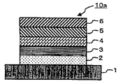
尚、有機電界発光素子の有機層とは、下記詳述するが、陽極と陰極との間に有する層であって、有機化合物を含有する層をいう。具体的には、正孔注入層、正孔輸送層、電子阻止層、発光層、正孔阻止層、電子輸送層、電子注入層などの有機層を指す。
<有機溶媒>
本発明の有機電界発光素子用組成物は、2種類以上の有機溶媒を含有し、有機溶媒のうち少なくとも2種は、その沸点が互いに20℃以上の差を有することを特徴とする。少なくとも2種の有機溶媒は、好ましくは30℃以上の差を有することが好ましく、通常、40℃以上の差を有する。その沸点が互いに20℃以上の差を有することにより、ノズルの乾燥防止と塗布膜の均一乾燥を両立させる効果が得られる。尚、有機溶媒が3種類以上含有される場合は、少なくとも2種の沸点が互いに20℃以上の差であればよく、他の2種同士は20℃以上の差がなくてもよい。
The organic layer of the organic electroluminescent element is a layer between the anode and the cathode, which is described below in detail, and refers to a layer containing an organic compound. Specifically, it refers to organic layers such as a hole injection layer, a hole transport layer, an electron blocking layer, a light emitting layer, a hole blocking layer, an electron transport layer, and an electron injection layer.
<Organic solvent>
The composition for organic electroluminescent elements of the present invention contains two or more organic solvents, and at least two of the organic solvents have a difference in boiling point of 20 ° C. or more. The at least two organic solvents preferably have a difference of 30 ° C. or more, and usually have a difference of 40 ° C. or more. When the boiling points have a difference of 20 ° C. or more, an effect of achieving both prevention of nozzle drying and uniform drying of the coating film can be obtained. In addition, when three or more types of organic solvents are contained, it is sufficient that the boiling points of at least two types are different from each other by 20 ° C. or more, and the other two types may not have a difference of 20 ° C. or more.
有機溶媒は、2種以上含有されるが、好ましくは3種以下、さらに好ましくは2種である。
また、有機電界発光素子用組成物に含有される有機溶媒の含有比は、有機溶媒が2種類含まれる場合は、沸点が低い溶媒/沸点が高い溶媒=3/17〜17/3の範囲が好ましい。有機溶媒が3種類以上含まれる場合は、最も沸点が低い溶媒/最も沸点が高い溶媒の比率が上記範囲であることが好ましい。
Although 2 or more types of organic solvents are contained, Preferably they are 3 types or less, More preferably, they are 2 types.
Moreover, the content ratio of the organic solvent contained in the composition for organic electroluminescent elements has a range of 3/17 to 17/3, where two kinds of organic solvents are included, a solvent having a low boiling point / a solvent having a high boiling point = 3/17 to 17/3. preferable. When three or more kinds of organic solvents are contained, the ratio of the solvent having the lowest boiling point / the solvent having the highest boiling point is preferably within the above range.
ここで、本発明の有機電界発光素子用組成物に含有される有機溶媒としては、以下の溶媒が挙げられる。
例えば、エチレングリコールジメチルエーテル、エチレングリコールジエチルエーテル、プロピレングリコール−1−モノメチルエーテルアセタート(PGMEA)等の脂肪族エーテル; 1,2−ジメトキシベンゼン、1,3−ジメトキシベンゼン、アニソール、フェネトール、2−メトキシトルエン、3−メトキシトルエン、4−メトキシトルエン、2 , 3− ジメチルアニソール、2,4−ジメチルアニソール、トリフルオロメトキシアニソール、ペンタフルオロメトキシベンゼン、3−( トリフルオロメチル) アニソール等の芳香族エーテル;酢酸エチル、酢酸n−ブチル、乳酸エチル、乳酸n−ブチル等の脂肪族エステル; 酢酸フェニル、プロピオン酸フェニル、安息香酸メチル、安息香酸エチル、安息香酸イソプロピル、エチル( ペンタフルオロベンゾエート)等の芳香族エステル;アセトフェノン等の芳香族ケトン;2,4−ジメチルフェノール、2−エチルフェノール、3−エチルフェノール、3−ヒドロキシトルエン等のフェノール類、等の溶媒が挙げられる。これらは、沸点が230℃未満の有機溶媒である。中でも、安息香酸エチル、アセトフェノンが好ましい。
Here, the following solvents are mentioned as an organic solvent contained in the composition for organic electroluminescent elements of this invention.
For example, aliphatic ethers such as ethylene glycol dimethyl ether, ethylene glycol diethyl ether, propylene glycol-1-monomethyl ether acetate (PGMEA); 1,2-dimethoxybenzene, 1,3-dimethoxybenzene, anisole, phenetole, 2-methoxy Aromatic ethers such as toluene, 3-methoxytoluene, 4-methoxytoluene, 2,3-dimethylanisole, 2,4-dimethylanisole, trifluoromethoxyanisole, pentafluoromethoxybenzene, 3- (trifluoromethyl) anisole; Aliphatic esters such as ethyl acetate, n-butyl acetate, ethyl lactate, n-butyl lactate; phenyl acetate, phenyl propionate, methyl benzoate, ethyl benzoate, isopropyl benzoate, ethyl Examples include aromatic esters such as (pentafluorobenzoate); aromatic ketones such as acetophenone; and phenols such as 2,4-dimethylphenol, 2-ethylphenol, 3-ethylphenol, and 3-hydroxytoluene. . These are organic solvents having a boiling point of less than 230 ° C. Of these, ethyl benzoate and acetophenone are preferable.
また、例えば、ジエチレングリコールジ−n−ブチルエーテル等の脂肪族エーテル;トリアセチン、ラウリン酸メチル、テトラエチレングリコールジメチルエーテル、γ−デカノラクトン等の脂肪族エステル;1,3,5−トリイソプロピルベンゼン、シクロヘキシルベンゼン、1-メチルナフタレン、ジフェニルメタン等の芳香族;p−アニスアルデヒド、ジフェニルエーテル、ジベンジルエーテル等の芳香族エーテル;安息香酸n−ブチル、安息香酸n−ペンチル、安息香酸プロピル、酢酸2−フェノキシエチル、安息香酸イソアミル、フタル酸ジエチル等の芳香族エステル;1’−アセトナフトン等の芳香族ケトン;4−プロピルフェノール等のフェノール類、等の溶媒が挙げられる。これらは、沸点が230℃以上の有機溶媒である。中でも、ジフェニルエーテル、ジフェニルメタンが好ましい。 Further, for example, aliphatic ethers such as diethylene glycol di-n-butyl ether; aliphatic esters such as triacetin, methyl laurate, tetraethylene glycol dimethyl ether, and γ-decanolactone; 1,3,5-triisopropylbenzene, cyclohexylbenzene, 1 -Aromatics such as methylnaphthalene and diphenylmethane; aromatic ethers such as p-anisaldehyde, diphenyl ether and dibenzyl ether; n-butyl benzoate, n-pentyl benzoate, propyl benzoate, 2-phenoxyethyl acetate, benzoic acid Solvents such as aromatic esters such as isoamyl and diethyl phthalate; aromatic ketones such as 1′-acetonaphthone; phenols such as 4-propylphenol; These are organic solvents having a boiling point of 230 ° C. or higher. Of these, diphenyl ether and diphenylmethane are preferable.
また、本発明の有機電界発光素子用組成物は、安息香酸エチルとジフェニルエーテルが含まれていることが好ましく、特に溶媒としてこの2種のみが含まれていることが好ましい。
中でも、本発明の有機電界発光素子用組成物は、沸点230℃以上の有機溶媒を含有することが吐出安定性の確保のため好ましい。沸点は、240℃以上がより好ましく、さらに好ましくは250℃以上、通常300℃以下である。
Moreover, the composition for organic electroluminescent elements of the present invention preferably contains ethyl benzoate and diphenyl ether, and particularly preferably contains only these two types as a solvent.
Among these, the composition for organic electroluminescent elements of the present invention preferably contains an organic solvent having a boiling point of 230 ° C. or more for ensuring ejection stability. The boiling point is more preferably 240 ° C. or higher, further preferably 250 ° C. or higher, and usually 300 ° C. or lower.
特に、本発明の有機電界発光素子用組成物において、沸点230℃以上の有機溶媒は、15〜85重量%含有することが吐出安定性の点で好ましい。ここで、複数の有機溶媒が沸点230℃以上である場合には、その合計量が15〜85重量%である。
さらに、沸点230℃以上の有機溶媒は、下記詳述する溶質を2重量%以上溶解することが好ましく、4重量%以上溶解することがさらに好ましい。溶質を2重量%以上溶解することで、乾燥時の溶媒組成変化での析出を防ぎ、ベタ塗布面の均一性を得ることができる。
尚、ここでいう溶解とは、温度23℃、湿度50%、1気圧において溶解する量を意味する。
In particular, in the composition for organic electroluminescent elements of the present invention, the organic solvent having a boiling point of 230 ° C. or higher is preferably contained in an amount of 15 to 85% by weight from the viewpoint of ejection stability. Here, when the plurality of organic solvents has a boiling point of 230 ° C. or higher, the total amount is 15 to 85% by weight.
Furthermore, the organic solvent having a boiling point of 230 ° C. or higher preferably dissolves 2% by weight or more of the solute described in detail below, and more preferably 4% by weight or more. By dissolving 2% by weight or more of the solute, precipitation due to a change in the solvent composition during drying can be prevented, and uniformity of the solid coated surface can be obtained.
The dissolution here means the amount dissolved at a temperature of 23 ° C., a humidity of 50%, and an atmospheric pressure.
<溶質>
本発明の有機電界発光素子用組成物は、さらに溶質を含有することが好ましい。溶質は、有機電界発光素子の有機層を形成する化合物であって、従来公知の有機電界発光素子の有機層に用いられる化合物を使用できる。
<Solute>
It is preferable that the composition for organic electroluminescent elements of the present invention further contains a solute. The solute is a compound that forms the organic layer of the organic electroluminescent element, and a compound that is used in the organic layer of a conventionally known organic electroluminescent element can be used.
本発明の有機電界発光素子用組成物において、溶質は0.5重量%以上、好ましくは2重量%以上含有していることが好ましい。
中でも、本発明の有機電界発光素子用組成物は、溶質として正孔注入材料または正孔輸送材料を含有することが好ましい。ここで、正孔注入材料および正孔輸送材料としては、下記正孔注入層や正孔輸送層に用いられる材料が挙げられる。
ここで、溶質としては、下記式(1)で表される繰り返し単位からなるポリマーが好ましい。
In the composition for organic electroluminescent elements of the present invention, the solute is preferably contained in an amount of 0.5% by weight or more, preferably 2% by weight or more.
Especially, it is preferable that the composition for organic electroluminescent elements of this invention contains a hole injection material or a hole transport material as a solute. Here, examples of the hole injection material and the hole transport material include materials used for the following hole injection layer and hole transport layer.
Here, the solute is preferably a polymer composed of repeating units represented by the following formula (1).
(式(1)中、n:2〜1000)該ポリマーの重量平均分子量は、通常1000〜500000である。
上記式(1)で表される繰り返し単位からなるポリマーは、本発明の有機電界発光素子用組成物において、好ましくは0.1重量%以上、さらに好ましくは0.5重量%以上、好ましくは10重量%以下、さらに好ましくは5重量%以下含有される。
下記正孔注入層で詳細に説明するが、さらに溶質としては、以下のイオン化合物を含有することが好ましい。
(In formula (1), n: 2-1000) The weight average molecular weight of this polymer is 1000-500,000 normally.
The polymer comprising the repeating unit represented by the above formula (1) is preferably 0.1% by weight or more, more preferably 0.5% by weight or more, preferably 10% in the composition for organic electroluminescent elements of the present invention. It is contained by weight% or less, more preferably 5% by weight or less.
The hole injection layer will be described in detail below, but the solute preferably contains the following ionic compound.
上記イオン化合物は、本発明の有機電界発光素子用組成物において、好ましくは0.1重量%以上、さらに好ましくは1重量%以上、好ましくは60重量%以下、さらに好ましくは50重量%以下含有される。
また、本発明の有機電界発光素子用組成物は、上記式(1)で表される繰り返し単位からなるポリマーと該イオン化合物を含有することが好ましく、特に該ポリマー/該イオン化合物=10/1〜1/1であることが好ましい。
本発明の有機電界発光素子用組成物は、上記の他にも種々の化合物が含まれていてよいが、上述の通り、通常、有機電界発光素子の有機層を形成する化合物が含まれる。
In the composition for organic electroluminescent elements of the present invention, the ionic compound is preferably contained in an amount of 0.1% by weight or more, more preferably 1% by weight or more, preferably 60% by weight or less, more preferably 50% by weight or less. The
In addition, the composition for an organic electroluminescent element of the present invention preferably contains a polymer composed of a repeating unit represented by the above formula (1) and the ionic compound, and particularly the polymer / the ionic compound = 10/1. It is preferable to be 1/1.
Although the composition for organic electroluminescent elements of the present invention may contain various compounds in addition to the above, it usually contains a compound that forms the organic layer of the organic electroluminescent element as described above.
<接触角>
本発明の有機電界発光素子用組成物は、ガラス基材に対して5〜10度の接触角を有することを特徴とする。好ましくは7度以上、8度以下である。溶媒を2種以上含み、かつ、接触角を該範囲にすることにより、ノズルの乾き防止による吐出安定性と、適度な基材への濡れ性によるベタ塗布面の均一性とを両立することが出来る。
<Contact angle>
The composition for organic electroluminescent elements of the present invention has a contact angle of 5 to 10 degrees with respect to a glass substrate. Preferably, it is 7 degrees or more and 8 degrees or less. By including two or more solvents and making the contact angle in this range, it is possible to achieve both discharge stability by preventing the nozzle from drying and uniformity of the solid coating surface by appropriate wettability to the substrate. I can do it.
ここで、本発明における接触角の測定方法を詳細に説明する。ディスプレイ用ガラス基板(例:旭ガラス社製「AN100」)の研磨面を洗浄剤(例:ライオン社製「サンウォッシュTL−100」)によって洗浄後、UVオゾン処理(例:低圧水銀灯にて1000mj/cm2)することで光洗浄を施し、純水による接触角が0度、すなわち完全に濡れ拡がる清浄なガラス基板を準備する。次に市販の接触角測定装置(例:協和界面科学社製「CA−DT」)を使用し、25Gのテフロン(登録商標)被覆ステンレス針にて作成した300nlの液滴を上記基板上に着滴させた後、10秒経過時の接触角の値を、温度23℃湿度50%の環境にて測定する。
このように、有機電界発光素子用組成物の接触角を5〜10度とする方法は以下の通りである。接触角は液の物性値では一意的には決まらないが、通常は表面張力や粘度を高くすることで、接触角を高くすることが出来る。またガラス基材への親和性が高い溶媒の含有量を増やすと、接触角を低くすることが出来る。
Here, the method for measuring the contact angle in the present invention will be described in detail. The polished surface of a glass substrate for display (eg, “AN100” manufactured by Asahi Glass Co., Ltd.) is washed with a cleaning agent (eg, “Sunwash TL-100” manufactured by Lion Corporation), and then subjected to UV ozone treatment (eg, 1000 mj using a low-pressure mercury lamp). / Cm 2 ) to prepare a clean glass substrate having a contact angle with pure water of 0 °, that is, completely wet and spread. Next, using a commercially available contact angle measuring device (for example, “CA-DT” manufactured by Kyowa Interface Science Co., Ltd.), a 300 nl droplet created with a 25 G Teflon (registered trademark) coated stainless needle is deposited on the substrate. After dropping, the value of the contact angle when 10 seconds have elapsed is measured in an environment of a temperature of 23 ° C. and a humidity of 50%.
Thus, the method of setting the contact angle of the composition for organic electroluminescent elements to 5 to 10 degrees is as follows. Although the contact angle is not uniquely determined by the physical property value of the liquid, it is usually possible to increase the contact angle by increasing the surface tension and viscosity. Further, when the content of the solvent having high affinity for the glass substrate is increased, the contact angle can be lowered.
<液滴径>
本発明の有機電界発光素子用組成物は、さらに、インクジェット法で、20plの液滴サイズでガラス基材に着滴させたとき、着滴後1分経過後の液滴径が100〜400μmであることが好ましく、さらに好ましくは150μm以上、300μm以下である。これにより、膜厚ムラやピンホールの発生を防止し、かつ端部の直線性を確保することができる。
<Droplet diameter>
The composition for an organic electroluminescent device of the present invention further has a droplet diameter of 100 to 400 μm after the lapse of 1 minute after the droplet is deposited, when the droplet is deposited on a glass substrate with a droplet size of 20 pl by an inkjet method. It is preferable that the thickness is 150 μm or more and 300 μm or less. Thereby, it is possible to prevent the occurrence of film thickness unevenness and pinholes and to ensure the linearity of the end portion.
具体的に、液滴径の測定方法としては、ディスプレイ用ガラス基板(例:旭ガラス社製「AN100」)の研磨面を洗浄剤(例:ライオン社製「サンウォッシュTL−100」)によって洗浄後、UVオゾン処理(例:低圧水銀灯にて1000mj/cm2)することで光洗浄を施し、純水による接触角が0度、すなわち完全に濡れ拡がる清浄なガラス基板を準備する。次に市販のピエゾ方式のインクジェットプリンタヘッド(例:富士フィルムダイマティクス社製、商品名Spectra SE128)に充填した塗布液材料を、平均液滴サイズ20plにて基板上に500μm間隔で5mm×20mmのエリアに吐出し、温度23℃湿度50%の環境にて1分間静置した後の液滴を光学顕微鏡にて観察して液滴径を測定する。
インクジェット法による着滴径は濡れ拡がり性(接触角)と強い相関が見られるが、通常は粘度や表面張力を低くすることで、液滴径を大きくすることが出来る。またガラス基材への親和性が高い溶媒の含有量を増やすと、液滴径を大きくすることが出来る。
Specifically, as a method for measuring the droplet diameter, the polished surface of a glass substrate for display (eg, “AN100” manufactured by Asahi Glass Co., Ltd.) is cleaned with a cleaning agent (eg, “Sunwash TL-100” manufactured by Lion Corporation). Then, UV ozone treatment (for example, 1000 mj / cm 2 with a low-pressure mercury lamp) is used to perform light cleaning, and a clean glass substrate with a contact angle with pure water of 0 degrees, that is, completely wetted and spread, is prepared. Next, the coating liquid material filled in a commercially available piezo-type ink jet printer head (eg, Fujifilm Dimatics, trade name: Spectra SE128) is 5 mm × 20 mm at an interval of 500 μm on the substrate with an average droplet size of 20 pl. The droplet diameter is measured by observing the droplet after discharging to an area and leaving it still for 1 minute in an environment of temperature 23 ° C. and humidity 50% with an optical microscope.
The droplet diameter obtained by the ink jet method has a strong correlation with the wet spreading property (contact angle). Usually, the droplet diameter can be increased by lowering the viscosity and the surface tension. Further, when the content of the solvent having a high affinity for the glass substrate is increased, the droplet diameter can be increased.
2.有機電界発光素子の製造方法
本発明は、また、インクジェット法で有機層を形成する有機電界発光素子の製造方法において、上記本発明の有機電界発光素子用組成物をベタ塗布して有機層を形成する有機電界発光素子の製造方法に関する。
2. The present invention also relates to a method for producing an organic electroluminescent element in which an organic layer is formed by an inkjet method, and the organic layer is formed by solid-coating the composition for an organic electroluminescent element of the present invention. The present invention relates to a method for manufacturing an organic electroluminescent element.
ここでベタ塗布とは、繰り返しパターン(例えば有機電界発光素子の場合は画素)のある一定以上の集合(例えば有機電界発光素子の場合はパネル)に対して、一括して略均一の膜厚で隙間なく塗布製膜することと定義される。具体的には、ディップ塗布、スピン塗布、スロットダイ塗布等はベタ塗布に好適な塗布方法であるが、基板内の塗布不要部分(例えば有機電界発光素子の場合はパネル間の余白部分)については、事前のマスキングや事後の拭き取りなどの操作が必要である。 Here, the solid coating is a uniform film thickness with respect to a certain set (for example, a panel in the case of an organic electroluminescent device) of a repetitive pattern (for example, a pixel in the case of an organic electroluminescent device). It is defined as coating with no gap. Specifically, dip coating, spin coating, slot die coating, and the like are suitable coating methods for solid coating, but for portions that do not require coating in the substrate (for example, a margin between panels in the case of an organic electroluminescent element) It is necessary to perform operations such as pre-masking and subsequent wiping.
一方、インクジェット法で有機層を形成する方法としては、上記したマスキングや拭き取りなどの操作が不要であることが大きな利点である。
また、本発明の製造方法によれば、ベタ塗布して得られた塗布面の端部の直線性が、該端部長さ10mmに対する真直度で500μm以内とすることが好ましい。これにより、パネルの周辺部での発光特性のばらつきが低減し、高性能な有機電界発光素子が得られる。
On the other hand, as a method of forming an organic layer by the inkjet method, it is a great advantage that operations such as masking and wiping described above are unnecessary.
Moreover, according to the manufacturing method of the present invention, it is preferable that the linearity of the end portion of the coated surface obtained by solid coating is within 500 μm in straightness with respect to the end length of 10 mm. Thereby, the dispersion | variation in the light emission characteristic in the peripheral part of a panel reduces, and a high performance organic electroluminescent element is obtained.
ベタ塗布して得られた塗布面の端部の直線性が、該端部長さ10mmに対する真直度で500μm以内とする方法としては、例えば、本発明での塗布液材料を用い、着滴径に対して着滴ピッチを若干狭く調整することが挙げられる。
また、本発明の製造方法によれば、ベタ塗布面の端部の膜厚均一性が、該端部から1mmの部分の膜厚が、ベタ塗布面の平均膜厚の80%以上120%以下であり、かつ該端部から1mm以内のうち最も厚い部分の膜厚がベタ塗布面の平均膜厚の400%以下とすることが好ましい。
As a method for making the linearity of the end of the coating surface obtained by solid coating within 500 μm in straightness with respect to the end length 10 mm, for example, using the coating liquid material in the present invention, On the other hand, adjusting the landing pitch slightly narrower is mentioned.
Further, according to the manufacturing method of the present invention, the film thickness uniformity at the end of the solid coating surface is such that the thickness of the
ベタ塗布面の端部の膜厚均一性が、該端部から1mmの部分の膜厚が、ベタ塗布面の平均膜厚の80%以上120%以下であり、かつ該端部から1mm以内のうち最も厚い部分の膜厚がベタ塗布面の平均膜厚の400%以下とする方法としては、例えば、本発明の塗布液材料を用い、塗布完了後に減圧乾燥等の方法によって速やかに塗膜を乾燥させること、が挙げられる。 The film thickness uniformity at the edge of the solid coated surface is 1% from the edge, and the film thickness is 80% to 120% of the average film thickness of the solid coated surface, and within 1 mm from the edge. As the method of setting the film thickness of the thickest part to 400% or less of the average film thickness of the solid coating surface, for example, using the coating liquid material of the present invention, the coating film can be quickly applied by a method such as reduced-pressure drying after the coating is completed. Drying.
3.有機電界発光素子
本発明の有機電界発光素子は、上記本発明の有機電界発光素子用組成物を用いて形成された有機層を有することを特徴とする。
ここで、本発明の有機電界発光素子(以下、有機EL素子と呼ぶ場合がある)は、通常、基板を備え、当該基板上に第1の電極が形成され、その上に上述の各層が積層された積層型の構成を有するものである。ここで、第1の電極及び第2の電極は、何れかが陽極であり、他方が陰極である。以下、第1の電極が陽極、第2の電極が陰極である場合について、基板側から積層される順に説明する。
3. Organic electroluminescent element The organic electroluminescent element of this invention has an organic layer formed using the composition for organic electroluminescent elements of the said invention.
Here, the organic electroluminescent element of the present invention (hereinafter sometimes referred to as an organic EL element) usually includes a substrate, a first electrode is formed on the substrate, and the above-described layers are stacked thereon. It has a laminated type structure. Here, one of the first electrode and the second electrode is an anode, and the other is a cathode. Hereinafter, the case where the first electrode is an anode and the second electrode is a cathode will be described in the order of stacking from the substrate side.
図1は、本発明の有機EL素子の構造の一例を模式的に示す断面図である。図1に示す有機EL素子10aは、基板1の上に、陽極2、正孔注入層3、発光層4、電子輸送層5、及び陰極6を、この順に積層して構成される。本発明の有機電界発光素子用組成物を用いて形成された層は、陽極2及び陰極6の間に有する有機層であればいずれの層にも適用できるが、特に、正孔注入層に適用することが好ましい。
FIG. 1 is a cross-sectional view schematically showing an example of the structure of the organic EL element of the present invention. An
<1.基板>
基板1は有機EL素子10aの支持体となるものであり、石英やガラスの板、金属板や金属箔、プラスチックフィルムやシート等が用いられる。特にガラス板や、ポリエステル、ポリメタクリレート、ポリカーボネート、ポリスルホン等の透明な合成樹脂の板等、汎用材料からなる透明基板を用いることが好ましい。
<1. Substrate>
The
基板1の材料の例としては、BK7、SF11、LaSFN9、BaK1、F2などの
各種ショットガラス、合成フェーズドシリカガラス、光学クラウンガラス、低膨張ボロシリケートガラス、サファイヤガラス、ソーダガラス、無アルカリガラスなどのガラス、TFTが形成されたガラス、高分子材料としては、ポリメチルメタクリレートや架橋アクリレートなどのアクリル樹脂、ピスフェノールAポリカーボネートなどの芳香族ポリカーボネート樹脂、ポリエチレンテレフタレートなどのポリエステル樹脂、ポリシクロオレフィンなどの非晶性ポリオレフィン樹脂、エポキシ樹脂、ポリスチレンなどのスチレン樹脂、ポリエーテルスルホンなどのポリスルホン樹脂、ポリエーテルイミド樹脂などの合成樹脂、等が挙げられる。また、これらのうち2種以上の積層体であってもよい。目的と用途に応じて、これらの基板の上に反射防止フィルム、円偏光フィルム、位相差フィルムなどの光学フィルムを形成、若しくは張り合わせてもよい。
Examples of the material of the
ただし、合成樹脂基板を使用する場合にはガスバリア性に留意することが好ましい。基板1のガスバリア性が小さすぎると、基板1を通過した外気により有機EL素子10aが劣化する可能性があるからである。このため、合成樹脂基板の少なくとも片面に緻密なシリコン酸化膜等を設けてガスバリア性を確保する方法も好ましい方法の一つである。
However, it is preferable to pay attention to gas barrier properties when using a synthetic resin substrate. This is because if the gas barrier property of the
<2.陽極>
基板1上には、例えば陽極2が設けられる。陽極2は、発光層4側の層(正孔注入層3または発光層4等)への正孔注入の役割を果たすものである。
この陽極2は、通常、アルミニウム、金、銀、ニッケル、パラジウム、白金等の金属;インジウム及び/またはスズの酸化物等の金属酸化物;ヨウ化銅等のハロゲン化金属;カーボンブラック、或いは、ポリ(3−メチルチオフェン)、ポリピロール、ポリアニリン等の導電性高分子等により構成される。なお、陽極2の材料は、1種のみを用いてもよく、2種以上を任意の組み合わせ及び比率で併用してもよい。
<2. Anode>
On the
This
陽極2の形成方法に制限は無いが、通常、スパッタリング法、蒸着法等により行われる。また、銀等の金属微粒子、ヨウ化銅等の微粒子、カーボンブラック、導電性の金属酸化物微粒子、導電性高分子微粉末等を用いて陽極2を形成する場合には、適当なバインダ樹脂溶液にそれらを分散させて、基板1上に塗布することにより陽極2を形成することもできる。さらに、導電性高分子の場合は、電解重合により直接基板1上に薄膜を形成したり、基板1上に導電性高分子を塗布して陽極2を形成することもできる(Appl.Phys.Lett.,60巻,2711頁,1992年)。
Although there is no restriction | limiting in the formation method of the
また、陽極2は通常は単層構造であるが、所望により複数の材料からなる積層構造とすることも可能である。
陽極2の厚みは、必要とする透明性により異なる。透明性が必要とされる場合は、可視
光の透過率を、通常60%以上、中でも80%以上とすることが好ましく、この場合、陽極2の厚みは、通常5nm以上、中でも10nm以上が好ましく、また、通常1000nm以下、中でも500nm以下が好ましい。一方、陽極2が不透明でよい場合、陽極2の厚みは任意であり、陽極2は基板1と同一でもよい。さらに、上記の陽極2の上に異なる導電材料を積層することも可能である。
In addition, the
The thickness of the
The light transmittance is usually 60% or more, preferably 80% or more. In this case, the thickness of the
また、陽極2に付着した不純物を除去し、イオン化ポテンシャルを調整して正孔注入性を向上させることを目的として、陽極2の表面を紫外線(UV)/オゾン処理したり、酸素プラズマ、アルゴンプラズマ処理したりすることが好ましい。
さらに、正孔注入の効率を更に向上させ、かつ、有機層全体の陽極への付着力を改善させる目的で、正孔注入層3と陽極2との間に公知の陽極バッファ層を挿入してもよい。
<3.正孔注入層>
正孔注入層3は、陽極2から発光層4へ正孔を輸送する層である。以下、まず正孔注入
層3に含有される成分を説明し、次に正孔注入層3の形成方法について説明する。
Further, for the purpose of removing impurities adhering to the
Furthermore, a known anode buffer layer is inserted between the hole injection layer 3 and the
<3. Hole injection layer>
The hole injection layer 3 is a layer that transports holes from the
〔3−1.正孔注入層の材料〕
正孔注入層の材料(正孔注入材料)は、正孔注入層3に含有されるものである。また、正孔注入層3を湿式成膜法で形成する場合は、正孔注入層用の塗布用組成物(本発明の有機電界発光素子用組成物)にも、正孔注入層の材料が含有される。この正孔注入層の材料は、正孔注入層3を形成しうるものであれば特に制限は無い。ただし、通常は、正孔注入層の材料として、高分子化合物(以下、適宜ポリマーともいう)及び電子受容性化合物を用いる。さらに、正孔注入層の材料として、それ以外の成分を用いてもよい。以下、これらの正孔注入層の材料について説明する。
[3-1. (Material for hole injection layer)
The material of the hole injection layer (hole injection material) is contained in the hole injection layer 3. Further, when the hole injection layer 3 is formed by a wet film forming method, the material for the hole injection layer is also used in the coating composition for the hole injection layer (the composition for the organic electroluminescence device of the present invention). Contained. The material of the hole injection layer is not particularly limited as long as it can form the hole injection layer 3. However, normally, a polymer compound (hereinafter also referred to as a polymer as appropriate) and an electron-accepting compound are used as the material for the hole injection layer. Further, other components may be used as the material for the hole injection layer. Hereinafter, materials of these hole injection layers will be described.
(3−1−1.ポリマー)
正孔注入層の材料として用いられるポリマーの種類は、本発明の効果を著しく損なわない限り任意である。ただし、その中でも、正孔輸送性を有するポリマー(高分子量の正孔輸送性化合物(以下適宜、「正孔輸送性ポリマー」という。)が好ましく、この観点から、4.5eV〜5.5eVのイオン化ポテンシャルを有する化合物であることが好ましい。なお、イオン化ポテンシャルは物質のHOMO(最高被占分子軌道)レベルにある電子を真空準位に放出するのに必要なエネルギーで定義され、光電子分光法で直接測定されるか、電気化学的に測定した参加電位を基準電極に対して補正して求められる。後者の方法の場合は、例えば、飽和甘コウ電極(SCE)を基準電極として用いたとき、下記式で表される(“Molecular Semiconductors”, Springer−Verlag, 1985年, pp.98)。
(3-1-1. Polymer)
The type of the polymer used as the material for the hole injection layer is arbitrary as long as the effects of the present invention are not significantly impaired. However, among them, a polymer having a hole transporting property (a high molecular weight hole transporting compound (hereinafter, appropriately referred to as “hole transporting polymer”) is preferable, and from this viewpoint, it is 4.5 eV to 5.5 eV. Preferably, the compound has an ionization potential, which is defined by the energy required to emit electrons at the HOMO (highest occupied molecular orbital) level of the material to the vacuum level. In the case of the latter method, for example, when a saturated sweet potato electrode (SCE) is used as a reference electrode, it is obtained by correcting the participation potential measured directly or electrochemically with respect to the reference electrode. It is represented by the following formula ("Molecular Semiconductors", Springer-Verlag, 1985, pp. 98).
イオン化ポテンシャル = 酸化電位(vs.SCE)+4.3eV
前記正孔輸送性ポリマーの例としては、芳香族アミン化合物、フタロシアニン誘導体、ポルフィリン誘導体、オリゴチオフェン誘導体等が挙げられる。中でも、非晶質性、溶媒への溶解度、可視光の透過率の点から、芳香族アミン化合物が好ましい。
芳香族アミン化合物の中でも、特に芳香族三級アミン化合物が好ましい。なお、ここでいう芳香族三級アミン化合物とは、芳香族三級アミン構造を有する化合物であって、芳香族三級アミン由来の基を有する化合物も含む。
Ionization potential = oxidation potential (vs. SCE) + 4.3 eV
Examples of the hole transporting polymer include aromatic amine compounds, phthalocyanine derivatives, porphyrin derivatives, oligothiophene derivatives, and the like. Among these, an aromatic amine compound is preferable from the viewpoint of amorphousness, solubility in a solvent, and transmittance of visible light.
Of the aromatic amine compounds, aromatic tertiary amine compounds are particularly preferable. In addition, the aromatic tertiary amine compound here is a compound having an aromatic tertiary amine structure, and includes a compound having a group derived from an aromatic tertiary amine.
芳香族三級アミン化合物の種類は特に制限されないが、表面平滑化効果の点から、重量平均分子量が1000以上、100万以下の高分子化合物が更に好ましい。
芳香族三級アミン高分子化合物の好ましい例として、下記式(I)で表わされる繰り返し単位を有する高分子化合物が挙げられる。
The type of the aromatic tertiary amine compound is not particularly limited, but a polymer compound having a weight average molecular weight of 1,000 or more and 1,000,000 or less is more preferable from the viewpoint of the surface smoothing effect.
Preferable examples of the aromatic tertiary amine polymer compound include a polymer compound having a repeating unit represented by the following formula (I).
(式(I)中、Ar1及びAr2は各々独立して、置換基を有していてもよい芳香族炭化水素基、又は、置換基を有していてもよい芳香族複素環基を表わす。Ar3〜Ar5は各々独立して、置換基を有していてもよい2価の芳香族炭化水素基、又は、置換基を有していてもよい2価の芳香族複素環基を表わす。Xは、下記の連結基群X1の中から選ばれる連結
基を表わす。)
・連結基群X1:
(In the formula (I), Ar 1 and Ar 2 each independently represent an aromatic hydrocarbon group which may have a substituent, or an aromatic heterocyclic group which may have a substituent. Ar 3 to Ar 5 each independently represents a divalent aromatic hydrocarbon group which may have a substituent, or a divalent aromatic heterocyclic group which may have a substituent. X represents a linking group selected from the following linking group group X1.)
Linking group group X1:
(式中、Ar11〜Ar28は各々独立して、置換基を有していてもよい芳香族炭化水素基又は芳香族複素環基を表わす。R1及びR2は各々独立して、水素原子又は任意の置換基を表わす。)
前記式(I)において、Ar1〜Ar5及びAr11〜Ar28としては、任意の芳香族炭化水素環又は芳香族複素環由来の、1価又は2価の基が適用可能である。即ち、Ar1、A r2、Ar16、Ar21及びAr26は、それぞれ1価の基が適用可能であり、Ar3〜Ar5 、Ar11〜Ar15、Ar17〜Ar20、Ar22〜Ar25、Ar27及びAr28は、それぞれ2価の基が適用可能である。これらは各々同一であっても、互いに異なっていてもよい。また、任意の置換基を有していてもよい。
(In the formula, each of Ar 11 to Ar 28 independently represents an optionally substituted aromatic hydrocarbon group or aromatic heterocyclic group. R 1 and R 2 each independently represents hydrogen. Represents an atom or any substituent.)
In the formula (I), as Ar 1 to Ar 5 and Ar 11 to Ar 28 , any monovalent or divalent group derived from any aromatic hydrocarbon ring or aromatic heterocyclic ring is applicable. That is, each of Ar 1 , Ar 2 , Ar 16 , Ar 21, and Ar 26 can be a monovalent group. Ar 3 to Ar 5 , Ar 11 to Ar 15 , Ar 17 to Ar 20 , Ar 22 A divalent group can be applied to each of Ar 25 , Ar 27, and Ar 28 . These may be the same or different from each other. Moreover, you may have arbitrary substituents.
前記の芳香族炭化水素環としては、例えば、5又は6員環の単環又は2〜5縮合環が挙げられる。その具体例としては、ベンゼン環、ナフタレン環、アントラセン環、フェナントレン環、ペリレン環、テトラセン環、ピレン環、ベンズピレン環、クリセン環、トリフェニレン環、アセナフテン環、フルオランテン環、フルオレン環などが挙げられる。
前記の芳香族複素環としては、例えば、5又は6員環の単環又は2〜4縮合環が挙げられる。その具体例としては、フラン環、ベンゾフラン環、チオフェン環、ベンゾチオフェン環、ピロール環、ピラゾール環、イミダゾール環、オキサジアゾール環、インドール環、カルバゾール環、ピロロイミダゾール環、ピロロピラゾール環、ピロロピロール環、チエノピロール環、チエノチオフェン環、フロピロール環、フロフラン環、チエノフラン環、ベンゾイソオキサゾール環、ベンゾイソチアゾール環、ベンゾイミダゾール環、ピリジン環、ピラジン環、ピリダジン環、ピリミジン環、トリアジン環、キノリン環、イソキノリン環、シノリン環、キノキサリン環、フェナントリジン環、ベンゾイミダゾール環、ペリミジン環、キナゾリン環、キナゾリノン環、アズレン環などが挙げられる。
Examples of the aromatic hydrocarbon ring include a 5- or 6-membered monocyclic ring or a 2-5 condensed ring. Specific examples thereof include a benzene ring, naphthalene ring, anthracene ring, phenanthrene ring, perylene ring, tetracene ring, pyrene ring, benzpyrene ring, chrysene ring, triphenylene ring, acenaphthene ring, fluoranthene ring, and fluorene ring.
Examples of the aromatic heterocycle include a 5- or 6-membered monocyclic ring or a 2-4 condensed ring. Specific examples thereof include furan ring, benzofuran ring, thiophene ring, benzothiophene ring, pyrrole ring, pyrazole ring, imidazole ring, oxadiazole ring, indole ring, carbazole ring, pyrroloimidazole ring, pyrrolopyrazole ring, pyrrolopyrrole ring. , Thienopyrrole ring, thienothiophene ring, furopyrrole ring, furofuran ring, thienofuran ring, benzisoxazole ring, benzisothiazole ring, benzimidazole ring, pyridine ring, pyrazine ring, pyridazine ring, pyrimidine ring, triazine ring, quinoline ring, isoquinoline Ring, cinolin ring, quinoxaline ring, phenanthridine ring, benzimidazole ring, perimidine ring, quinazoline ring, quinazolinone ring, azulene ring and the like.
また、Ar3〜Ar5、Ar11〜Ar15、Ar17〜Ar20、Ar22〜Ar25、Ar27、Ar28としては、上に例示した1種類又は2種類以上の芳香族炭化水素環及び/又は芳香族複素環由来の2価の基を2つ以上連結して用いることもできる。
さらに、Ar1〜Ar5及びAr11〜Ar28の芳香族炭化水素環及び/又は芳香族複素環由来の基は、本発明の趣旨に反しない限りにおいて、更に置換基を有していてもよい。置換基の分子量としては、通常400以下、中でも250以下程度が好ましい。置換基の種類は特に制限されないが、例としては、下記の置換基群Wから選ばれる1種又は2種以上が挙げられる。なお、置換基は、1個が単独で置換していてもよく、2個以上が任意の組
み合わせ及び比率で置換していてもよい。
Ar 3 to Ar 5 , Ar 11 to Ar 15 , Ar 17 to Ar 20 , Ar 22 to Ar 25 , Ar 27 , Ar 28 may be one type or two or more types of aromatic hydrocarbon rings exemplified above. And / or two or more divalent groups derived from an aromatic heterocycle may be linked and used.
Furthermore, the group derived from the aromatic hydrocarbon ring and / or aromatic heterocycle of Ar 1 to Ar 5 and Ar 11 to Ar 28 may further have a substituent unless it is contrary to the gist of the present invention. Good. The molecular weight of the substituent is usually 400 or less, preferably about 250 or less. The type of the substituent is not particularly limited, and examples thereof include one or more selected from the following substituent group W. In addition, as for a substituent, 1 piece may be substituted independently and 2 or more may be substituted by arbitrary combinations and ratios.
[置換基群W]
メチル基、エチル基等の、炭素数が通常1以上、通常10以下、好ましくは8以下のアルキル基;ビニル基等の、炭素数が通常2以上、通常11以下、好ましくは5以下のアルケニル基;エチニル基等の、炭素数が通常2以上、通常11以下、好ましくは5以下のアルキニル基;メトキシ基、エトキシ基等の、炭素数が通常1以上、通常10以下、好ましくは6以下のアルコキシ基;フェノキシ基、ナフトキシ基、ピリジルオキシ基等の、炭素数が通常4以上、好ましくは5以上、通常25以下、好ましくは14以下のアリールオキシ基;メトキシカルボニル基、エトキシカルボニル基等の、炭素数が通常2以上、通常11以下、好ましくは7以下のアルコキシカルボニル基;ジメチルアミノ基、ジエチルアミノ基等の、炭素数が通常2以上、通常20以下、好ましくは12以下のジアルキルアミノ基;ジフェニルアミノ基、ジトリルアミノ基、N−カルバゾリル基等の、炭素数が通常10以上、好ましくは12以上、通常30以下、好ましくは22以下のジアリールアミノ基;フェニルメチルアミノ基等の、炭素数が通常6以上、好ましくは7以上、通常25以下、好ましくは17以下のアリールアルキルアミノ基;アセチル基、ベンゾイル基等の、炭素数が通常2以上、通常10以下、好ましくは7以下のアシル基;フッ素原子、塩素原子等のハロゲン原子;トリフルオロメチル基等の、炭素数が通常1以上、通常8以下、好ましくは4以下のハロアルキル基;メチルチオ基、エチルチオ基等の、炭素数が通常1以上、通常10以下、好ましくは6以下のアルキルチオ基;フェニルチオ基、ナフチルチオ基、ピリジルチオ基等の、炭素数が通常4以上、好ましくは5以上、通常25以下、好ましくは14以下のアリールチオ基;トリメチルシリル基、トリフェニルシリル基等の、炭素数が通常2以上、好ましくは3以上、通常33以下、好ましくは26以下のシリル基;トリメチルシロキシ基、トリフェニルシロキシ基等の、炭素数が通常2以上、好ましくは3以上、通常33以下、好ましくは26以下のシロキシ基;シアノ基;フェニル基、ナフチル基等の、炭素数が通常6以上、通常30以下、好ましくは18以下の芳香族炭化水素環基;チエニル基、ピリジル基等の、炭素数が通常3以上、好ましくは4以上、通常28以下、好ましくは17以下の芳香族複素環基。
[Substituent group W]
An alkyl group having usually 1 or more, usually 10 or less, preferably 8 or less, such as a methyl group or an ethyl group; an alkenyl group having 2 or more, usually 11 or less, preferably 5 or less carbon atoms, such as a vinyl group. An alkynyl group having usually 2 or more, usually 11 or less, preferably 5 or less, such as an ethynyl group; an alkoxy having a carbon number of usually 1 or more, usually 10 or less, preferably 6 or less, such as a methoxy group or an ethoxy group; A group; an aryloxy group such as a phenoxy group, a naphthoxy group, a pyridyloxy group, etc., usually 4 or more, preferably 5 or more, usually 25 or less, preferably 14 or less; a carbon such as a methoxycarbonyl group or an ethoxycarbonyl group An alkoxycarbonyl group having a number of usually 2 or more, usually 11 or less, preferably 7 or less; a dimethylamino group, a diethylamino group or the like, and usually having 2 or more carbon atoms Usually 20 or less, preferably 12 or less dialkylamino group; diphenylamino group, ditolylamino group, N-carbazolyl group, etc., and usually diarylamino having 10 or more carbon atoms, preferably 12 or more, usually 30 or less, preferably 22 or less Group: an arylalkylamino group having 6 or more carbon atoms, preferably 7 or more, usually 25 or less, preferably 17 or less, such as a phenylmethylamino group; an acetyl group, a benzoyl group or the like, and usually having 2 or more carbon atoms, Usually an acyl group of 10 or less, preferably 7 or less; a halogen atom such as a fluorine atom or a chlorine atom; a haloalkyl group having a carbon number of usually 1 or more, usually 8 or less, preferably 4 or less, such as a trifluoromethyl group; An alkylthio group having 1 to 10 carbon atoms, preferably 6 or less, preferably 6 or less; An arylthio group having a carbon number of usually 4 or more, preferably 5 or more, usually 25 or less, preferably 14 or less, such as a ruthio group, a naphthylthio group, or a pyridylthio group; Or more, preferably 3 or more, usually 33 or less, preferably 26 or less silyl group; trimethylsiloxy group, triphenylsiloxy group, etc., the carbon number is usually 2 or more, preferably 3 or more, usually 33 or less, preferably 26 or less. A siloxy group; a cyano group; an aromatic hydrocarbon ring group having usually 6 or more, usually 30 or less, preferably 18 or less, such as a phenyl group or a naphthyl group; a carbon number such as a thienyl group or a pyridyl group. An aromatic heterocyclic group of 3 or more, preferably 4 or more, usually 28 or less, preferably 17 or less.
上述したものの中でも、Ar1及びAr2としては、高分子化合物の溶解性、耐熱性、正孔注入・輸送性の点から、ベンゼン環、ナフタレン環、フェナントレン環、チオフェン環、ピリジン環由来の1価の基が好ましく、フェニル基、ナフチル基が更に好ましい。
また、上述したものの中でも、Ar3〜Ar5としては、耐熱性、酸化還元電位を含めた正孔注入・輸送性の点から、ベンゼン環、ナフタレン環、アントラセン環、フェナントレ
ン環由来の2価の基が好ましく、フェニレン基、ビフェニレン基、ナフチレン基が更に好ましい。
Among those described above, Ar 1 and Ar 2 are 1 derived from a benzene ring, a naphthalene ring, a phenanthrene ring, a thiophene ring, and a pyridine ring from the viewpoint of the solubility, heat resistance, and hole injection / transport properties of the polymer compound. Is more preferably a phenyl group or a naphthyl group.
Among these, Ar 3 to Ar 5 are benzene ring, naphthalene ring, anthracene ring, phenanthrene from the viewpoint of heat resistance and hole injection / transport properties including redox potential.
A divalent group derived from an aromatic ring is preferable, and a phenylene group, a biphenylene group, and a naphthylene group are more preferable.
前記式(I)において、R1及びR2としては、水素原子又は任意の置換基が適用可能である。これらは互いに同一であってもよく、異なっていてもよい。置換基の種類は、本発明の趣旨に反しない限り特に制限されないが、適用可能な置換基を例示するならば、アルキル基、アルケニル基、アルキニル基、アルコキシ基、シリル基、シロキシ基、芳香族炭化水素基、芳香族複素環基が挙げられる。これらの具体例としては、先に置換基群Wにおいて例示した各基が挙げられる。 In the formula (I), as R 1 and R 2 , a hydrogen atom or an arbitrary substituent is applicable. These may be the same or different from each other. The type of the substituent is not particularly limited as long as it is not contrary to the gist of the present invention. However, if applicable substituents are exemplified, an alkyl group, an alkenyl group, an alkynyl group, an alkoxy group, a silyl group, a siloxy group, an aromatic group A hydrocarbon group and an aromatic heterocyclic group are mentioned. Specific examples thereof include the groups exemplified above in the substituent group W.
前記式(I)の中でも、上記式(1)で表される繰り返し単位からなるポリマーが好ましい。
正孔注入層の材料として用いられる正孔輸送性ポリマーの重量平均分子量は本発明の効果を著しく損なわない限り任意であるが、通常1000以上、好ましくは2000以上、より好ましくは3000以上、また、通常50万以下、好ましくは20万以下、より好ま
しくは10万以下である。
Among the formula (I), a polymer composed of a repeating unit represented by the above formula (1) is preferable.
The weight average molecular weight of the hole transporting polymer used as the material of the hole injection layer is arbitrary as long as the effect of the present invention is not significantly impaired, but is usually 1000 or more, preferably 2000 or more, more preferably 3000 or more, Usually, it is 500,000 or less, preferably 200,000 or less, more preferably 100,000 or less.
正孔注入層3中のポリマーの割合は、本発明の効果を著しく損なわない限り任意であるが、正孔注入層3全体に対する重量比の値で、通常10重量%以上、好ましくは30重量%以上、また、通常99.9重量%以下、好ましくは99重量%以下である。なお、2種以上のポリマーを併用する場合には、これらの合計の含有量が上記範囲に含まれるようにすることが好ましい。 The ratio of the polymer in the hole injection layer 3 is arbitrary as long as the effect of the present invention is not significantly impaired, but is usually 10% by weight or more, preferably 30% by weight in terms of the weight ratio with respect to the whole hole injection layer 3. In addition, it is usually 99.9% by weight or less, preferably 99% by weight or less. In addition, when using 2 or more types of polymers together, it is preferable that these total content is contained in the said range.
(2−3−1−2.電子受容性化合物)
正孔注入層の材料として用いられる電子受容性化合物の種類は、本発明の効果を著しく損なわない限り任意である。その例としては、4−イソプロピル−4’−メチルジフェニルヨードニウムテトラキス(ペンタフルオロフェニル)ボラート、トリフェニルスルホニウムテトラフルオロボラート等の有機基の置換したオニウム塩;塩化鉄(III)(特開平 11−251067号公報)、ペルオキソ二硫酸アンモニウム等の高原子価の無機化合物;テトラシアノエチレン等のシアノ化合物、トリス(ペンダフルオロフェニル)ボラン(特開2003−31365号公報)等の芳香族ホウ素化合物;フラーレン誘導体;ヨウ素等が挙げられる。上記の化合物のうち、強い酸化力を有する点で、有機基の置換したオニウム塩、高原子価の無機化合物が好ましく、種々の溶媒に可溶である点で、有機基の置換したオニウム塩、シアノ化合物、芳香族ホウ素化合物が好ましい。さらに、強い酸化力と高い溶解性とを両立する点から、有機基の置換したオニウム塩が最も好ましく、下記式(II−1)〜(II−3)で表わされる化合物であることが特に好ましい。
(2-3-1-2. Electron-accepting compound)
The kind of the electron accepting compound used as the material for the hole injection layer is arbitrary as long as the effects of the present invention are not significantly impaired. Examples thereof include onium salts substituted with an organic group such as 4-isopropyl-4′-methyldiphenyliodonium tetrakis (pentafluorophenyl) borate and triphenylsulfonium tetrafluoroborate; No. 251067), high-valence inorganic compounds such as ammonium peroxodisulfate; cyano compounds such as tetracyanoethylene; aromatic boron compounds such as tris (pendafluorophenyl) borane (JP-A-2003-31365); fullerene derivatives ; Iodine etc. are mentioned. Among the above compounds, an onium salt substituted with an organic group is preferable in terms of having strong oxidizing power, and an inorganic compound having a high valence is preferable, and an onium salt substituted with an organic group in terms of being soluble in various solvents, A cyano compound and an aromatic boron compound are preferable. Furthermore, an onium salt substituted with an organic group is most preferable from the viewpoint of achieving both strong oxidizing power and high solubility, and particularly preferably a compound represented by the following formulas (II-1) to (II-3). .
(上記式(II−1)〜(II−3)中、R11、R21及びR31は、各々独立に、A1〜A3と炭素原子で結合する有機基を表わす。R12、R22、R23及びR32〜R34は、各々独立に、任意の基を表わす。R11〜R34のうち隣接する2以上の基が、互いに結合して環を形成していてもよい。A1〜A3は何れも長周期型周期表(以下、特に断り書きの無い限り「周期表」という場合には、長周期型周期表を指すものとする。)第3周期以降の元素であって、A1は周期表の第17族に属する元素を表わし、A2は周期表の第16族に属する元素を表わし、A3は周期表の第15族に属する元素を表わす。Z1 n1-〜Z3 n3-は、各々独立に、 対アニオンを表わす。n1〜n3は、各々独立に、対アニオンのイオン価を表わす。)
上記式(II−1)〜(II−3)中、R11、R21及びR31は、各々独立に、A1〜A3と炭素原子で結合する有機基を表わす。したがって、R11、R21及びR31としては、A1〜A3との結合部分に炭素原子を有する有機基であれば、本発明の趣旨に反しない限り、その種類は特に制限されない。
(In the above formulas (II-1) to (II-3), R 11 , R 21 and R 31 each independently represents an organic group bonded to A 1 to A 3 via a carbon atom. R 12 , R 22 , R 23 and R 32 to R 34 each independently represents an arbitrary group, and two or more adjacent groups of R 11 to R 34 may be bonded to each other to form a ring. A 1 -A 3 are all elements in the long period type periodic table (hereinafter, unless otherwise specified, the term “periodic table” refers to the long period type periodic table). there are, a 1 represents an element belonging to group 17 of the periodic table, a 2 represents an element belonging to group 16 of the periodic table, a 3 is .Z 1 representing an element belonging to group 15 of the periodic table n1- to Z 3 n3- each independently represents a counter anion, and n 1 to n 3 each independently represents an ionic value of the counter anion.)
In the above formulas (II-1) to (II-3), R 11 , R 21 and R 31 each independently represents an organic group bonded to A 1 to A 3 via a carbon atom. Therefore, as R 11 , R 21, and R 31 , the type is not particularly limited as long as it is an organic group having a carbon atom at the bond portion with A 1 to A 3 unless it is contrary to the gist of the present invention.
R11、R21及びR31の分子量は、それぞれ、その置換基を含めた値で、通常1000以下、好ましくは500以下の範囲である。
R11、R21及びR31の好ましい例としては、正電荷を非局在化させる点から、アルキル基、アルケニル基、アルキニル基、芳香族炭化水素基、芳香族複素環基が挙げられる。中でも、正電荷を非局在化させるとともに熱的に安定であることから、芳香族炭化水素基又は芳香族複素環基が好ましい。
The molecular weights of R 11 , R 21 and R 31 are each a value including the substituent, and are usually 1000 or less, preferably 500 or less.
Preferred examples of R 11 , R 21 and R 31 include alkyl groups, alkenyl groups, alkynyl groups, aromatic hydrocarbon groups, and aromatic heterocyclic groups from the viewpoint of delocalizing positive charges. Among them, an aromatic hydrocarbon group or an aromatic heterocyclic group is preferable because it delocalizes positive charges and is thermally stable.
アルキル基としては、例えば、直鎖状、分岐鎖状又は環状のアルキル基であって、その炭素数が通常1以上、また、通常12以下、好ましくは6以下のものが挙げられる。具体例としては、メチル基、エチル基、n−プロピル基、2−プロピル基、n−ブチル基、イソブチル基、tert−ブチル基、シクロヘキシル基等が挙げられる。
アルケニル基としては、例えば、炭素数が通常2以上、通常12以下、好ましくは6以下のものが挙げられる。具体例としては、ビニル基、アリル基、1−ブテニル基等が挙げられる。
The alkyl group includes, for example, a linear, branched or cyclic alkyl group having a carbon number of usually 1 or more and usually 12 or less, preferably 6 or less. Specific examples include methyl group, ethyl group, n-propyl group, 2-propyl group, n-butyl group, isobutyl group, tert-butyl group, cyclohexyl group and the like.
Examples of the alkenyl group include those having usually 2 or more, usually 12 or less, preferably 6 or less carbon atoms. Specific examples include a vinyl group, an allyl group, and a 1-butenyl group.
アルキニル基としては、例えば、炭素数が通常2以上、通常12以下、好ましくは6以下のものが挙げられる。具体例としては、エチニル基、プロパルギル基等が挙げられる。
芳香族炭化水素基としては、例えば、5又は6員環の単環又は2〜5縮合環由来の1価の基であり、正電荷を当該基上により非局在化させられる基が挙げられる。その具体例としては、ベンゼン環、ナフタレン環、アントラセン環、フェナントレン環、ペリレン環、テトラセン環、ピレン環、ベンズピレン環、クリセン環、トリフェニレン環、アセナフテン環、フルオレン環等の由来の一価の基が挙げられる。
Examples of the alkynyl group include those having usually 2 or more, usually 12 or less, preferably 6 or less. Specific examples include ethynyl group and propargyl group.
Examples of the aromatic hydrocarbon group include a monovalent group derived from a 5- or 6-membered monocyclic ring or a 2 to 5 condensed ring, and a group in which a positive charge is delocalized on the group. . Specific examples thereof include monovalent groups derived from a benzene ring, naphthalene ring, anthracene ring, phenanthrene ring, perylene ring, tetracene ring, pyrene ring, benzpyrene ring, chrysene ring, triphenylene ring, acenaphthene ring, fluorene ring, and the like. Can be mentioned.
芳香族複素環基としては、例えば、5又は6員環の単環又は2〜4縮合環由来の1価の基であり、正電荷を当該基上により非局在化させられる基が挙げられる。その具体例としては、フラン環、ベンゾフラン環、チオフェン環、ベンゾチオフェン環、ピロール環、ピラゾール環、トリアゾール環、イミダゾール環、オキサジアゾール環、インドール環、カルバゾール環、ピロロイミダゾール環、ピロロピラゾール環、ピロロピロール環、チエノピロール環、チエノチオフェン環、フロピロール環、フロフラン環、チエノフラン環、ベンゾイソオキサゾール環、ベンゾイソチアゾール環、ベンゾイミダゾール環、ピリジン環、ピラジン環、ピリダジン環、ピリミジン環、トリアジン環、キノリン環、イソキノリン環、シノリン環、キノキサリン環、フェナントリジン環、ベンゾイミダゾール環、ペリミジン環、キナゾリン環、キナゾリノン環、アズレン環等の由来の一価の基が挙げられる。 Examples of the aromatic heterocyclic group include a monovalent group derived from a 5- or 6-membered monocyclic ring or a 2-4 condensed ring, and a group in which a positive charge is delocalized on the group. . Specific examples thereof include furan ring, benzofuran ring, thiophene ring, benzothiophene ring, pyrrole ring, pyrazole ring, triazole ring, imidazole ring, oxadiazole ring, indole ring, carbazole ring, pyrroloimidazole ring, pyrrolopyrazole ring, Pyrrolopyrrole ring, thienopyrrole ring, thienothiophene ring, furopyrrole ring, furofuran ring, thienofuran ring, benzisoxazole ring, benzisothiazole ring, benzimidazole ring, pyridine ring, pyrazine ring, pyridazine ring, pyrimidine ring, triazine ring, quinoline And monovalent groups derived from a ring, an isoquinoline ring, a sinoline ring, a quinoxaline ring, a phenanthridine ring, a benzimidazole ring, a perimidine ring, a quinazoline ring, a quinazolinone ring, an azulene ring, and the like.
上記式(II−1)〜(II−3)中、R12、R22、R23及びR32〜R34は、各々独立に、任意の置換基を表わす。したがって、R12、R22、R23及びR32〜R34の種類は、本発明の趣旨に反しない限り特に制限されない。
R12、R22、R23及びR32〜R34の分子量は、それぞれ、その置換基を含めた値で、通常1000以下、好ましくは500以下の範囲である。
In the above formulas (II-1) to (II-3), R 12 , R 22 , R 23 and R 32 to R 34 each independently represents an arbitrary substituent. Accordingly, the types of R 12 , R 22 , R 23 and R 32 to R 34 are not particularly limited as long as they are not contrary to the spirit of the present invention.
The molecular weights of R 12 , R 22 , R 23 and R 32 to R 34 are each a value including the substituent, and are usually 1000 or less, preferably 500 or less.
R12、R22、R23及びR32〜R34の例としては、アルキル基、アルケニル基、アルキニル基、芳香族炭化水素基、芳香族複素環基、アミノ基、アルキルアミノ基、アリールアミノ基、アシルアミノ基、アルコキシ基、アリールオキシ基、アシル基、アルコキシカルボニル基、アリールオキシカルボニル基、アルキルカルボニルオキシ基、アルキルチオ基、アリールチオ基、スルホニル基、アルキルスルホニル基、アリールスルホニル基、スルホニルオキシ基、シアノ基、水酸基、チオール基、シリル基等が挙げられる。中でも、R11、R21及びR31と同様、電子受容性が大きい点から、A1〜A3との結合部分に炭素原子を有する有機基が好ましく、例としては、アルキル基、アルケニル基、アルキニル基、芳香族炭化水素基、芳香族複素環基が好ましい。特に、電子受容性が大きいとともに熱的に安定であることから、芳香族炭化水素基又は芳香族複素環基が好ましい。 Examples of R 12 , R 22 , R 23 and R 32 to R 34 are alkyl groups, alkenyl groups, alkynyl groups, aromatic hydrocarbon groups, aromatic heterocyclic groups, amino groups, alkylamino groups, arylamino groups. , Acylamino group, alkoxy group, aryloxy group, acyl group, alkoxycarbonyl group, aryloxycarbonyl group, alkylcarbonyloxy group, alkylthio group, arylthio group, sulfonyl group, alkylsulfonyl group, arylsulfonyl group, sulfonyloxy group, cyano Group, hydroxyl group, thiol group, silyl group and the like. Among them, like R 11 , R 21, and R 31 , an organic group having a carbon atom at the bond portion with A 1 to A 3 is preferable from the viewpoint of high electron acceptability. Examples include an alkyl group, an alkenyl group, Alkynyl groups, aromatic hydrocarbon groups, and aromatic heterocyclic groups are preferred. In particular, an aromatic hydrocarbon group or an aromatic heterocyclic group is preferable because it has a large electron accepting property and is thermally stable.
アルキル基、アルケニル基、アルキニル基、芳香族炭化水素基、芳香族複素環基としては、R11、R21及びR31について先に説明したものと同様のものが挙げられる。
以上、R11、R21、R31、R12、R22、R23、及びR32〜R34として例示した基は、本発明の趣旨に反しない限りにおいて、更に他の置換基によって置換されていてもよい。置換基の種類は特に制限されないが、例としては、上記R11、R21、R31、R12、R22、R23、及びR32〜R34としてそれぞれ例示した基の他、ハロゲン原子、シアノ基、チオシアノ基、ニトロ基等が挙げられる。中でも、耐熱性及び電子受容性の妨げにならない観点から、アルキル基、アルケニル基、アルキニル基、アルコキシ基、アリールオキシ基、芳香族炭化水素基、芳香族複素環基が好ましい。なお、前記の更に置換する置換基は、1個のみで置換していてもよく、2個以上が任意の組み合わせ及び比率で置換していてもよい。
Examples of the alkyl group, alkenyl group, alkynyl group, aromatic hydrocarbon group and aromatic heterocyclic group are the same as those described above for R 11 , R 21 and R 31 .
As described above, the groups exemplified as R 11 , R 21 , R 31 , R 12 , R 22 , R 23 , and R 32 to R 34 are further substituted with other substituents unless they are contrary to the spirit of the present invention. It may be. The type of the substituent is not particularly limited, and examples thereof include a halogen atom in addition to the groups exemplified as R 11 , R 21 , R 31 , R 12 , R 22 , R 23 , and R 32 to R 34 . A cyano group, a thiocyano group, a nitro group, etc. are mentioned. Among these, an alkyl group, an alkenyl group, an alkynyl group, an alkoxy group, an aryloxy group, an aromatic hydrocarbon group, and an aromatic heterocyclic group are preferable from the viewpoint of not hindering heat resistance and electron accepting property. In addition, the substituent to be further substituted may be substituted with only one, or two or more may be substituted with any combination and ratio.
また、上記式(II−1)〜(II−3)中、R11〜R34のうち隣接する2以上の基は、互いに結合して環を形成していてもよい。
式(II−1)〜(II−3)中、A1〜A3は、何れも周期表第3周期以降(第3〜第6周期)の元素であって、A1は、長周期型周期表の第17族に属する元素を表わし、A2は、第16族に属する元素を表わし、A3は、第15族に属する元素を表わす。
In the formulas (II-1) to (II-3), two or more adjacent groups out of R 11 to R 34 may be bonded to each other to form a ring.
In formulas (II-1) to (II-3), A 1 to A 3 are all elements from the third period (third to sixth periods) of the periodic table, and A 1 is a long-period type An element belonging to Group 17 of the periodic table is represented, A 2 represents an element belonging to Group 16 and A 3 represents an element belonging to Group 15.
中でも、電子受容性及び入手容易性の観点から、周期表の第5周期以前(第3〜第5周期)の元素が好ましい。即ち、A1としてはヨウ素原子、臭素原子、塩素原子のうち何れ かが好ましく、A2としてはテルル原子、セレン原子、硫黄原子のうち何れかが好ましく 、A3としてはアンチモン原子、ヒ素原子、リン原子のうち何れかが好ましい。
特に、電子受容性、化合物の安定性の面から、式(II−1)におけるA1が臭素原子又 はヨウ素原子である化合物、又は、式(II−2)におけるA2がセレン原子又は硫黄原子 である化合物が好ましく、中でも、式(II−1)におけるA1がヨウ素原子である化合物 が特に好ましい。
Among these, from the viewpoint of electron acceptability and availability, elements before the fifth period (third to fifth periods) of the periodic table are preferable. That is, A 1 is preferably any of iodine, bromine, and chlorine, A 2 is preferably any of tellurium, selenium, or sulfur, and A 3 is antimony, arsenic, Any of the phosphorus atoms is preferred.
In particular, from the viewpoints of electron acceptability and compound stability, a compound in which A 1 in formula (II-1) is a bromine atom or an iodine atom, or A 2 in formula (II-2) is a selenium atom or sulfur. The compound which is an atom is preferable, and the compound in which A 1 in formula (II-1) is an iodine atom is particularly preferable.
式(II−1)〜(II−3)中、Z1 n1-〜Z3 n3-は、各々独立に、対アニオンを表わす。対アニオンの種類は特に制限されず、単原子イオンであっても錯イオンであってもよい。但し、対アニオンのサイズが大きいほど負電荷が非局在化し、それに伴い正電荷も非局在化して電子受容能が大きくなるため、単原子イオンよりも錯イオンの方が好ましい。
式(II−1)〜(II−3)中、n1〜n3は、各々独立に、対アニオンZ1 n1-〜Z3 n3-のイオン価に相当する任意の正の整数である。n1〜n3の値は特に制限されないが、何れも1又は2であることが好ましく、1であることが特に好ましい。
In formulas (II-1) to (II-3), Z 1 n1- to Z 3 n3- each independently represents a counter anion. The type of the counter anion is not particularly limited, and may be a monoatomic ion or a complex ion. However, the larger the size of the counter anion, the more the negative charge is delocalized, and the positive charge is also delocalized thereby increasing the electron accepting ability. Therefore, the complex ion is preferable to the monoatomic ion.
In formulas (II-1) to (II-3), n 1 to n 3 are each independently any positive integer corresponding to the ionic valence of counter anions Z 1 n1 to Z 3 n3− . The values of n 1 to n 3 are not particularly limited, but all are preferably 1 or 2, and particularly preferably 1.
Z1 n1-〜Z3 n3-の具体例としては、水酸化物イオン、フッ化物イオン、塩化物イオン、臭化物イオン、ヨウ化物イオン、シアン化物イオン、硝酸イオン、亜硝酸イオン、硫酸イ
オン、亜硫酸イオン、過塩素酸イオン、過臭素酸イオン、過ヨウ素酸イオン、塩素酸イオン、亜塩素酸イオン、次亜塩素酸イオン、リン酸イオン、亜リン酸イオン、次亜リン酸イオン、ホウ酸イオン、イソシアン酸イオン、水硫化物イオン、テトラフルオロホウ酸イオン、ヘキサフルオロリン酸イオン、ヘキサクロロアンチモン酸イオン;酢酸イオン、トリフルオロ酢酸イオン、安息香酸イオン等のカルボン酸イオン;メタンスルホン酸イオン、トリフルオロメタンスルホン酸イオン等のスルホン酸イオン;メトキシイオン、t−ブトキシイオン等のアルコキシイオンなどが挙げられる。
Specific examples of Z 1 n1- to Z 3 n3- include hydroxide ion, fluoride ion, chloride ion, bromide ion, iodide ion, cyanide ion, nitrate ion, nitrite ion, sulfate ion, sulfite. Ion, perchlorate ion, perbromate ion, periodate ion, chlorate ion, chlorite ion, hypochlorite ion, phosphate ion, phosphite ion, hypophosphite ion, borate ion , Isocyanate ion, hydrosulfide ion, tetrafluoroborate ion, hexafluorophosphate ion, hexachloroantimonate ion; carboxylate ion such as acetate ion, trifluoroacetate ion, benzoate ion; methanesulfonate ion, trifluoro Sulfonate ions such as romethanesulfonate ion; Alkoxy ions such as methoxy ion and t-butoxy ion For example.
特に、対アニオンZ1 n1-〜Z3 n3-としては、化合物の安定性、溶媒への溶解性の点で、下記式(II−4)〜(II−6)で表わされる錯イオンが好ましく、サイズが大きいという点で、負電荷が非局在化し、それに伴い正電荷も非局在化して電子受容能が大きくなるため、下記式(II−6)で表わされる錯イオンが更に好ましい。 In particular, as the counter anions Z 1 n1 to Z 3 n3 −, complex ions represented by the following formulas (II-4) to (II-6) are preferable from the viewpoint of stability of the compound and solubility in a solvent. In view of the large size, the negative charge is delocalized, and the positive charge is also delocalized to increase the electron accepting ability. Therefore, a complex ion represented by the following formula (II-6) is more preferable.
式(II−4)及び(II−6)中、E1及びE3は、各々独立に、長周期型周期表の第13族に属する元素を表わす。中でもホウ素原子、アルミニウム原子、ガリウム原子が好ましく、化合物の安定性、合成及び精製のし易さの点から、ホウ素原子が好ましい。
式(II−5)中、E2は、長周期型周期表の第15族に属する元素を表わす。中でもリ ン原子、ヒ素原子、アンチモン原子が好ましく、化合物の安定性、合成及び精製のし易さ、毒性の点から、リン原子が好ましい。
In formulas (II-4) and (II-6), E 1 and E 3 each independently represents an element belonging to Group 13 of the long-period periodic table. Of these, a boron atom, an aluminum atom, and a gallium atom are preferable, and a boron atom is preferable from the viewpoint of stability of the compound and ease of synthesis and purification.
In formula (II-5), E 2 represents an element belonging to Group 15 of the long-period periodic table. Among these, a phosphorus atom, an arsenic atom, and an antimony atom are preferable, and a phosphorus atom is preferable from the viewpoint of stability of the compound, easiness of synthesis and purification, and toxicity.
式(II−4)及び(II−5)中、Xは、フッ素原子、塩素原子、臭素原子などのハロゲン原子を表わし、化合物の安定性、合成及び精製のし易さの点からフッ素原子、塩素原子であることが好ましく、フッ素原子であることが特に好ましい。
式(II−6)中、Ar61〜Ar64は、各々独立に、芳香族炭化水素基又は芳香族複素環基を表わす。芳香族炭化水素基、芳香族複素環基の例示としては、R11、R21及びR31について先に例示したものと同様の、5又は6員環の単環又は2〜4縮合環由来の1価の基が挙げられる。中でも、化合物の安定性、耐熱性の点から、ベンゼン環、ナフタレン環、ピリジン環、ピラジン環、ピリダジン環、ピリミジン環、トリアジン環、キノリン環、イソキノリン環由来の1価の基が好ましい。
In the formulas (II-4) and (II-5), X represents a halogen atom such as a fluorine atom, a chlorine atom, or a bromine atom, and is a fluorine atom in terms of stability of the compound, ease of synthesis and purification, A chlorine atom is preferable, and a fluorine atom is particularly preferable.
In formula (II-6), Ar 61 to Ar 64 each independently represents an aromatic hydrocarbon group or an aromatic heterocyclic group. Examples of the aromatic hydrocarbon group and aromatic heterocyclic group are derived from the same 5- or 6-membered monocyclic ring or 2-4 condensed ring as those exemplified above for R 11 , R 21 and R 31 . A monovalent group is mentioned. Among these, a monovalent group derived from a benzene ring, a naphthalene ring, a pyridine ring, a pyrazine ring, a pyridazine ring, a pyrimidine ring, a triazine ring, a quinoline ring, or an isoquinoline ring is preferable from the viewpoint of stability and heat resistance of the compound.
Ar61〜Ar64として例示した芳香族炭化水素基、芳香族複素環基は、本発明の趣旨に反しない限りにおいて、更に別の置換基によって置換されていてもよい。置換基の種類は特に制限されず、任意の置換基が適用可能であるが、電子吸引性の基であることが好まし
い。
Ar61〜Ar64が有してもよい置換基として好ましい電子吸引性の基を例示するならば、フッ素原子、塩素原子、臭素原子等のハロゲン原子;シアノ基;チオシアノ基;ニトロ基;メシル基等のアルキルスルホニル基;トシル基等のアリールスルホニル基;ホルミル基、アセチル基、ベンゾイル基等の、炭素数が通常1以上、通常12以下、好ましくは6以下のアシル基;メトキシカルボニル基、エトキシカルボニル基等の、炭素数が通常2以上、通常10以下、好ましくは7以下のアルコキシカルボニル基;フェノキシカルボニル基、ピリジルオキシカルボニル基等の、炭素数が通常3以上、好ましくは4以上、通常25以下、好ましくは15以下の芳香族炭化水素基又は芳香族複素環基を有するアリールオキシカルボニル基;アミノカルボニル基;アミノスルホニル基;トリフルオロメチル基、ペンタフルオロエチル基等の、炭素数が通常1以上、通常10以下、好ましくは6以下の直鎖状、分岐鎖状又は環状のアルキル基にフッ素原子、塩素原子などのハロゲン原子が置換したハロアルキル基、などが挙げられる。
The aromatic hydrocarbon group and aromatic heterocyclic group exemplified as Ar 61 to Ar 64 may be further substituted with another substituent as long as not departing from the gist of the present invention. The type of the substituent is not particularly limited, and any substituent can be applied, but an electron-withdrawing group is preferable.
Examples of preferable electron-withdrawing groups as the substituent that Ar 61 to Ar 64 may have include halogen atoms such as fluorine atom, chlorine atom and bromine atom; cyano group; thiocyano group; nitro group; mesyl group Alkylsulfonyl groups such as tosyl group; arylsulfonyl groups such as tosyl group; acyl groups such as formyl group, acetyl group, benzoyl group and the like, usually having 1 or more, usually 12 or less, preferably 6 or less; methoxycarbonyl group, ethoxycarbonyl An alkoxycarbonyl group having 2 or more carbon atoms, usually 10 or less, preferably 7 or less; a phenoxycarbonyl group, a pyridyloxycarbonyl group or the like, and usually having 3 or more carbon atoms, preferably 4 or more and usually 25 or less. An aryloxycarbonyl group having an aromatic hydrocarbon group or an aromatic heterocyclic group of preferably 15 or less; Bonyl group; aminosulfonyl group; trifluoromethyl group, pentafluoroethyl group, etc., a fluorine atom in a linear, branched or cyclic alkyl group having usually 1 or more, usually 10 or less, preferably 6 or less carbon atoms And a haloalkyl group substituted with a halogen atom such as a chlorine atom.
中でも、Ar61〜Ar64のうち少なくとも1つの基が、フッ素原子又は塩素原子を置換基として1つ又は2つ以上有することがより好ましい。特に、負電荷を効率よく非局在化する点、及び、適度な昇華性を有する点から、Ar61〜Ar64の水素原子がすべてフッ素原子で置換されたパーフルオロアリール基であることが特に好ましい。パーフルオロアリール基の具体例としては、ペンタフルオロフェニル基、ヘプタフルオロ−2−ナフチル基、テトラフルオロ−4−ピリジル基等が挙げられる。
なお、前記の置換基は、1個のみが置換していてもよく、2個以上が任意の組み合わせ及び比率で置換していてもよい。
Especially, it is more preferable that at least one group among Ar 61 to Ar 64 has one or two or more fluorine atoms or chlorine atoms as substituents. In particular, it is particularly a perfluoroaryl group in which all the hydrogen atoms of Ar 61 to Ar 64 are substituted with fluorine atoms from the viewpoint of efficiently delocalizing negative charges and having a suitable sublimation property. preferable. Specific examples of the perfluoroaryl group include a pentafluorophenyl group, a heptafluoro-2-naphthyl group, and a tetrafluoro-4-pyridyl group.
In addition, as for the said substituent, only one may be substituted and two or more may be substituted by arbitrary combinations and ratios.
式(II−4)〜(II−6)で表わされる錯イオンの式量は、本発明の効果を著しく損なわない限り任意であるが、通常100以上、好ましくは300以上、更に好ましくは400以上、また、通常5000以下、好ましくは3000以下、更に好ましくは2000以下の範囲である。該錯イオンの式量が小さ過ぎると、正電荷及び負電荷の非局在化が不十分なため、電子受容能が低下する場合があり、また、該錯イオンの式量が大き過ぎると、該化合物自体が電荷輸送の妨げとなる場合がある。 The formula amount of the complex ions represented by the formulas (II-4) to (II-6) is arbitrary as long as the effect of the present invention is not significantly impaired, but is usually 100 or more, preferably 300 or more, more preferably 400 or more. Moreover, it is usually 5000 or less, preferably 3000 or less, more preferably 2000 or less. If the formula amount of the complex ion is too small, delocalization of the positive charge and the negative charge is insufficient, so that the electron accepting ability may be decreased, and if the formula amount of the complex ion is too large, The compound itself may interfere with charge transport.
正孔注入層の材料としては、上に説明した各種の電子受容性化合物のうち、何れか1種を単独で用いてもよく、2種以上を任意の組み合わせ及び比率で用いてもよい。2種以上の電子受容性化合物を用いる場合には、上記式(II−1)〜(II−3)のうち何れか1つの式に該当する電子受容性化合物を2種以上組み合わせてもよく、それぞれ異なる式に該当する2種以上の電子受容性化合物を組み合わせてもよい。 As the material for the hole injection layer, any one of the various electron-accepting compounds described above may be used alone, or two or more may be used in any combination and ratio. When two or more kinds of electron-accepting compounds are used, two or more kinds of electron-accepting compounds corresponding to any one of the formulas (II-1) to (II-3) may be combined. Two or more electron-accepting compounds corresponding to different formulas may be combined.
正孔注入層3及び正孔注入層用組成物中における電子受容性化合物の含有量は、本発明の効果を著しく損なわない限り任意であるが、ポリマー及び後述の正孔輸送性化合物に対する値で、通常0.1重量%以上、好ましくは1重量%以上、また、通常100重量%以下、好ましくは60重量%以下、更に好ましくは50重量%以下である。電子受容性化合物の量は多い方が不溶化しやすいため好ましく、加熱時間が短時間で不溶化することができる。なお、2種以上の電子受容性化合物を併用する場合には、これらの合計の含有量が上記範囲に含まれるようにする。 The content of the electron-accepting compound in the hole-injecting layer 3 and the composition for the hole-injecting layer is arbitrary as long as the effect of the present invention is not significantly impaired, but is a value with respect to the polymer and the hole-transporting compound described later. The amount is usually 0.1% by weight or more, preferably 1% by weight or more, and usually 100% by weight or less, preferably 60% by weight or less, more preferably 50% by weight or less. A larger amount of the electron-accepting compound is preferable because it is easier to insolubilize, and the heating time can be insolubilized in a short time. In addition, when using together 2 or more types of electron-accepting compounds, it is made for the total content of these to be contained in the said range.
なお、正孔注入層3の形成時或いは形成後に、上記の正孔輸送性を有するポリマー或いは下記の正孔輸送性化合物が、この電子受容性化合物と反応することにより、形成後の正孔注入層3中では、正孔輸送性ポリマー或いは正孔輸送性化合物のカチオンラジカル及びイオン化合物が生成している場合がある。 In addition, when the hole injection layer 3 is formed or after the formation, the above hole transporting polymer or the following hole transporting compound reacts with the electron accepting compound, so that the hole injection after the formation is performed. In the layer 3, a cation radical and an ionic compound of a hole transporting polymer or a hole transporting compound may be generated.
(3−1−3.低分子量の正孔輸送性化合物)
正孔注入層の材料としては、必要に応じて低分子量の正孔輸送性化合物を用いることが好ましい。
低分子量の正孔輸送性化合物は、従来、有機EL素子における正孔注入・輸送性の薄膜精製材料として利用されてきた各種の化合物の中から、適宜選択することが可能である。中でも、溶媒溶解性の高いものが好ましい。
低分子量の正孔輸送性化合物の好ましい例としては、芳香族アミン化合物が挙げられる。中でも、芳香族三級アミン化合物が特に好ましい。
(3-1-3. Low molecular weight hole transporting compound)
As a material for the hole injection layer, it is preferable to use a low molecular weight hole transporting compound as necessary.
The low molecular weight hole transporting compound can be appropriately selected from various compounds conventionally used as a hole injection / transport thin film purification material in an organic EL device. Among them, those having high solvent solubility are preferable.
Preferable examples of the low molecular weight hole transporting compound include aromatic amine compounds. Of these, aromatic tertiary amine compounds are particularly preferred.
なお、低分子量の正孔輸送性化合物の分子量は、本発明の効果を著しく損なわない限り任意であるが、通常200以上、好ましくは400以上、より好ましくは600以上、また、通常5000以下、好ましくは3000以下、より好ましくは2000以下、更に好ましくは1700以下、特に好ましくは1400以下の範囲である。分子量が小さ過ぎると耐熱性が低くなる傾向がある一方で、低分子量の正孔輸送性化合物の分子量が大き過ぎると合成及び精製が困難となる傾向がある。
なお、低分子量の正孔輸送性化合物は、1種のみを用いてもよく、2種以上を任意の組み合わせ及び比率で併用してもよい。
The molecular weight of the low molecular weight hole transporting compound is arbitrary as long as the effect of the present invention is not significantly impaired, but is usually 200 or more, preferably 400 or more, more preferably 600 or more, and usually 5000 or less, preferably Is not more than 3000, more preferably not more than 2000, still more preferably not more than 1700, particularly preferably not more than 1400. If the molecular weight is too small, the heat resistance tends to be low, whereas if the molecular weight of the low molecular weight hole transporting compound is too large, synthesis and purification tend to be difficult.
In addition, a low molecular weight hole transportable compound may use only 1 type, and may use 2 or more types together by arbitrary combinations and a ratio.
(3−1−4.その他の成分)
正孔注入層に含まれる材料としては、本発明の効果を著しく損なわない限り、上述したポリマー、電子受容性化合物及び正孔輸送性化合物に加えて、さらに、その他の成分を含有させても良い。その他の成分の例としては、各種の発光材料、電子輸送性化合物、バインダ樹脂、塗布性改良剤などが挙げられる。なお、その他の成分は、1種のみを用いてもよく、2種以上を任意の組み合わせ及び比率で併用してもよい。
(3-1-4. Other components)
As a material included in the hole injection layer, in addition to the above-described polymer, electron-accepting compound, and hole-transporting compound, other components may be further contained unless the effects of the present invention are significantly impaired. . Examples of other components include various light emitting materials, electron transporting compounds, binder resins, coatability improving agents, and the like. In addition, only 1 type may be used for another component and it may use 2 or more types together by arbitrary combinations and ratios.
〔3−2.正孔注入層の形成〕
正孔注入層の形成方法は特に限定されるものではなく、上述の材料に応じて適宜選択することができる。例えば湿式成膜法により正孔注入層3を形成する場合は、上述の材料を
適切な溶媒に溶解させて塗布用組成物(本発明の有機電界発光素子用組成物)を調製し、それを塗布及び乾燥することにより形成することができる。
[3-2. Formation of hole injection layer]
The method for forming the hole injection layer is not particularly limited, and can be appropriately selected depending on the above materials. For example, when the hole injection layer 3 is formed by a wet film forming method, the above-described materials are used.
It can be formed by dissolving in an appropriate solvent to prepare a coating composition (the composition for an organic electroluminescence device of the present invention), coating and drying it.
本発明においては、特に本発明の有機電界発光素子用組成物を用いて形成されることが好ましく、特に上記本発明の有機電界発光素子の製造方法として記載の方法により製造されることが好ましい。
塗布用組成物に含有させる正孔注入層用溶媒としては、正孔注入層3の形成が可能である限り任意のものを用いることができる。特に、本発明の有機電界発光素子用組成物に含まれる溶媒として記載のものが好ましい。
In the present invention, the organic electroluminescent element composition of the present invention is preferably used, and the organic electroluminescent element of the present invention is particularly preferably manufactured by the method described above.
As the hole injection layer solvent to be contained in the coating composition, any solvent can be used as long as the hole injection layer 3 can be formed. In particular, those described as the solvent contained in the composition for organic electroluminescent elements of the present invention are preferred.
塗布用組成物の塗布・成膜後、得られた塗膜を乾燥し、溶媒を除去することにより、正孔注入層が形成される。成膜の方式は、パターニングが可能な方法であれば、本発明の効果を著しく損なわない限り制限はない。例えば、スピンコート法、ディップコート法、ダイコート法、バーコート法、ブレードコート法、ロールコート法、スプレーコート法、キャピラリーコート法、インクジェット法、スクリーン印刷法、グラビア印刷法、フレキソ印刷法、等が挙げられる。 After coating and film-forming of the coating composition, the resulting coating film is dried and the solvent is removed to form a hole injection layer. The method of film formation is not limited as long as the effect of the present invention is not significantly impaired as long as patterning is possible. For example, spin coating method, dip coating method, die coating method, bar coating method, blade coating method, roll coating method, spray coating method, capillary coating method, ink jet method, screen printing method, gravure printing method, flexographic printing method, etc. Can be mentioned.
これらの成膜方法の中でも、スピンコート法、スプレーコート法、インクジェット法が好ましい。塗布用組成物に特有の液性に合うためである。
なお、乾燥の手法は例えば、プレート(ホットプレート)上に基材を搭載しそのプレートを介して塗布膜を加熱させるホットプレート方式、前記基材の上面側及び/又は下面側にヒーターを配置し、ヒーターから電磁波(例えば赤外線)を照射して、薄膜を加熱する
方式、等を用いることができる。加熱手段は1つでもよく、また2つ以上を任意の組み合わせ及び比率で用いてもよい。
なお、正孔注入層3の膜厚は本発明の効果を著しく損なわない限り任意であるが、通常5nm以上、好ましくは10nm以上、また、通常1000nm以下、好ましくは500nm以下の範囲である。
Among these film forming methods, a spin coating method, a spray coating method, and an ink jet method are preferable. This is because it matches the liquidity specific to the coating composition.
The drying method is, for example, a hot plate method in which a substrate is mounted on a plate (hot plate) and the coating film is heated through the plate, and a heater is disposed on the upper surface side and / or the lower surface side of the substrate. A method of heating the thin film by irradiating electromagnetic waves (for example, infrared rays) from a heater can be used. One heating means may be used, or two or more heating means may be used in any combination and ratio.
The thickness of the hole injection layer 3 is arbitrary as long as the effect of the present invention is not significantly impaired, but is usually 5 nm or more, preferably 10 nm or more, and usually 1000 nm or less, preferably 500 nm or less.
<4.発光層>
正孔注入層3の上には本発明に係る有機層として発光層4が設けられる。発光層4は、電界を与えられた電極間において、陽極2から正孔注入層3を通じて注入された正孔と、陰極6から電子輸送層5を通じて注入された電子との再結合により励起されて、主たる発光源となる層である。
<4. Light emitting layer>
A light emitting layer 4 is provided on the hole injection layer 3 as an organic layer according to the present invention. The light emitting layer 4 is excited by recombination of holes injected from the
〔4−1.発光層の材料〕
発光層4は、その構成材料として、少なくとも、発光の性質を有する材料(発光材料)を含有するとともに、好ましくは、正孔輸送の性質を有する化合物(正孔輸送性化合物)、あるいは、電子輸送の性質を有する化合物(電子輸送性化合物)を含有する。発光物質については特に限定はなく、所望の発光波長で発光し、発光効率が良好である物質を用いればよい。また、電荷輸送性化合物を2成分以上含有していることが好ましい。更に、発光層4は、本発明の効果を著しく損なわない範囲で、その他の成分を含有していてもよい。なお、本発明においては、何れも低分子化合物を使用することが好ましい。なお、低分子化合物とは、重量平均分子量が、通常6000以下、好ましくは5000以下、より好ましくは1500以下の化合物をいう。
[4-1. (Light emitting layer material)
The light emitting layer 4 contains at least a material having a light emitting property (light emitting material) as a constituent material, and preferably a compound having a hole transporting property (hole transporting compound) or an electron transport. A compound (electron transporting compound) having the following properties: There is no particular limitation on the light-emitting substance, and a substance that emits light at a desired emission wavelength and has high emission efficiency may be used. Moreover, it is preferable to contain two or more charge transport compounds. Furthermore, the light emitting layer 4 may contain other components as long as the effects of the present invention are not significantly impaired. In the present invention, it is preferable to use a low molecular weight compound. In addition, a low molecular compound means the compound whose weight average molecular weight is 6000 or less normally, Preferably it is 5000 or less, More preferably, it is 1500 or less.
(4−1−1.発光材料)
発光材料としては、任意の公知の材料を適用可能である。例えば、蛍光発光材料であってもよく、燐光発光材料であってもよいが、内部量子効率の観点から、好ましくは燐光発光材料である。
なお、溶媒への溶解性を向上させる目的で、発光材料の分子の対称性や剛性を低下させたり、或いはアルキル基などの親油性置換基を導入したりすることが好ましい。
(4-1-1. Light-Emitting Material)
Any known material can be applied as the light emitting material. For example, a fluorescent material or a phosphorescent material may be used, but a phosphorescent material is preferable from the viewpoint of internal quantum efficiency.
For the purpose of improving the solubility in a solvent, it is preferable to reduce the symmetry and rigidity of the molecules of the luminescent material or introduce a lipophilic substituent such as an alkyl group.
以下、発光材料のうち蛍光色素の例を挙げるが、蛍光色素は以下の例示物に限定されるものではない。
青色発光を与える蛍光色素(青色蛍光色素)としては、例えば、ペリレン、ピレン、アントラセン、クマリン、p−ビス(2−フェニルエテニル)ベンゼン及びそれらの誘導体等が挙げられる。
Hereinafter, although the example of a fluorescent dye is mentioned among light emitting materials, a fluorescent dye is not limited to the following illustrations.
Examples of the fluorescent dye that gives blue light emission (blue fluorescent dye) include perylene, pyrene, anthracene, coumarin, p-bis (2-phenylethenyl) benzene, and derivatives thereof.
緑色発光を与える蛍光色素(緑色蛍光色素)としては、例えば、キナクリドン誘導体、クマリン誘導体等が挙げられる。
黄色発光を与える蛍光色素(黄色蛍光色素)としては、例えば、ルブレン、ペリミドン誘導体等が挙げられる。
赤色発光を与える蛍光色素(赤色蛍光色素)としては、例えば、DCM(4−(dicyanomethylene)−2−methyl−6−(p−dimethylaminostyryl)−4H−pyran)系化合物、ベンゾピラン誘導体、ローダミン誘導体、ベンゾチオキサンテン誘導体、アザベンゾチオキサンテン等が挙げられる。
Examples of fluorescent dyes that give green light emission (green fluorescent dyes) include quinacridone derivatives and coumarin derivatives.
Examples of fluorescent dyes that give yellow light (yellow fluorescent dyes) include rubrene and perimidone derivatives.
Examples of fluorescent dyes that give red luminescence (red fluorescent dyes) include DCM (4- (dicyanomethylene) -2-methyl-6- (p-dimethylaminostyryl) -4H-pyran) compounds, benzopyran derivatives, rhodamine derivatives, benzoates. Examples thereof include thioxanthene derivatives and azabenzothioxanthene.
次に、発光材料のうち、燐光発光材料について説明する。燐光発光材料としては、例えば、周期表第7〜11族から選ばれる金属を含む有機金属錯体が挙げられる。
燐光性有機金属錯体に含まれる、周期表第7〜11族から選ばれる金属として、好ましいもの例を挙げると、ルテニウム、ロジウム、パラジウム、銀、レニウム、オスミウム、イリジウム、白金、金等が挙げられる。これらの有機金属錯体として、好ましくは下記式
(V)又は式(VI)で表わされる化合物が挙げられる。
Next, phosphorescent materials among the light emitting materials will be described. Examples of the phosphorescent material include an organometallic complex containing a metal selected from
Preferred examples of the metal selected from
ML(q-j)L′j (V)
{式(V)中、Mは金属を表わし、qは上記金属の価数を表わす。また、L及びL’は二座配位子を表わす。jは0、1又は2の数を表わす。}
ML ( qj ) L' j (V)
{In Formula (V), M represents a metal, and q represents the valence of the metal. L and L ′ represent bidentate ligands. j represents a number of 0, 1 or 2. }
{式(VI)中、M7は金属を表わし、Tは炭素原子又は窒素原子を表わす。R92〜R95は 、それぞれ独立に置換基を表わす。但し、Tが窒素原子の場合は、R94及びR95は無い。}
以下、まず、式(V)で表わされる化合物について説明する。
式(V)中、Mは任意の金属を表わし、好ましいものの具体例としては、周期表第7〜11族から選ばれる金属として前述した金属が挙げられる。
また、式(V)中、二座配位子Lは、以下の部分構造を有する配位子を示す。
{In Formula (VI), M 7 represents a metal, and T represents a carbon atom or a nitrogen atom. R 92 to R 95 each independently represents a substituent. However, when T is a nitrogen atom, R 94 and R 95 are absent. }
Hereinafter, the compound represented by the formula (V) will be described first.
In formula (V), M represents an arbitrary metal, and specific examples of preferable ones include the metals described above as metals selected from
In the formula (V), the bidentate ligand L represents a ligand having the following partial structure.
上記Lの部分構造において、環A1”は、置換基を有していてもよい、芳香族炭化水素基又は芳香族複素環基を表わす。
環A1”を構成する芳香族炭化水素基としては、例えば、5又は6員環の単環又は2〜5縮合環が挙げられる。その具体例としては、ベンゼン環、ナフタレン環、アントラセン環、フェナントレン環、ペリレン環、テトラセン環、ピレン環、ベンズピレン環、クリセン環、トリフェニレン環、アセナフテン環、フルオランテン環、フルオレン環由来の1価の基などが挙げられる。
In the partial structure of L, ring A1 ″ represents an aromatic hydrocarbon group or an aromatic heterocyclic group which may have a substituent.
Examples of the aromatic hydrocarbon group constituting the ring A1 ″ include a 5- or 6-membered monocyclic ring or a 2-5 condensed ring. Specific examples thereof include a benzene ring, a naphthalene ring, an anthracene ring, and a phenanthrene. And a monovalent group derived from a ring, a perylene ring, a tetracene ring, a pyrene ring, a benzpyrene ring, a chrysene ring, a triphenylene ring, an acenaphthene ring, a fluoranthene ring, and a fluorene ring.
環A1”を構成する芳香族複素環基としては、例えば、5又は6員環の単環又は2〜4縮合環が挙げられる。その具体例としては、フラン環、ベンゾフラン環、チオフェン環、ベンゾチオフェン環、ピロール環、ピラゾール環、イミダゾール環、オキサジアゾール環、インドール環、カルバゾール環、ピロロイミダゾール環、ピロロピラゾール環、ピロロピロール環、チエノピロール環、チエノチオフェン環、フロピロール環、フロフラン環、チエノフラン環、ベンゾイソオキサゾール環、ベンゾイソチアゾール環、ベンゾイミダゾール環、ピリジン環、ピラジン環、ピリダジン環、ピリミジン環、トリアジン環、キノリン環、イソキノリン環、シノリン環、キノキサリン環、フェナントリジン環、ベンゾイミダゾール環、ペリミジン環、キナゾリン環、キナゾリノン環、アズレン環由来の1価の基などが挙げられる。
また、上記Lの部分構造において、環A2は、置換基を有していてもよい、含窒素芳香族複素環基を表わす。
Examples of the aromatic heterocyclic group constituting the ring A1 ″ include a 5- or 6-membered monocyclic ring or a 2-4 condensed ring. Specific examples thereof include a furan ring, a benzofuran ring, a thiophene ring, and a benzoic ring. Thiophene ring, pyrrole ring, pyrazole ring, imidazole ring, oxadiazole ring, indole ring, carbazole ring, pyrroloimidazole ring, pyrrolopyrazole ring, pyrrolopyrrole ring, thienopyrrole ring, thienothiophene ring, furopyrrole ring, furofuran ring, thienofuran ring , Benzisoxazole ring, benzoisothiazole ring, benzimidazole ring, pyridine ring, pyrazine ring, pyridazine ring, pyrimidine ring, triazine ring, quinoline ring, isoquinoline ring, cinoline ring, quinoxaline ring, phenanthridine ring, benzimidazole ring , Perimidine ring, key Gelsolin ring, quinazolinone ring, and a monovalent group derived from azulene ring.
In the partial structure of L, ring A2 represents a nitrogen-containing aromatic heterocyclic group which may have a substituent.
環A2を構成する含窒素芳香族複素環基としては、例えば、5又は6員環の単環又は2〜4縮合環が挙げられる。その具体例としては、ピロール環、ピラゾール環、イミダゾール環、オキサジアゾール環、インドール環、カルバゾール環、ピロロイミダゾール環、ピロロピラゾール環、ピロロピロール環、チエノピロール環、フロピロール環、チエノフラン環、ベンゾイソオキサゾール環、ベンゾイソチアゾール環、ベンゾイミダゾール環、ピリジン環、ピラジン環、ピリダジン環、ピリミジン環、トリアジン環、キノリン環、イソキノリン環、キノキサリン環、フェナントリジン環、ベンゾイミダゾール環、ペリミジン環、キナゾリン環、キナゾリノン環由来の1価の基などが挙げられる。 Examples of the nitrogen-containing aromatic heterocyclic group constituting the ring A2 include a 5- or 6-membered monocyclic ring or a 2-4 condensed ring. Specific examples thereof include pyrrole ring, pyrazole ring, imidazole ring, oxadiazole ring, indole ring, carbazole ring, pyrroloimidazole ring, pyrrolopyrazole ring, pyrrolopyrrole ring, thienopyrrole ring, furopyrrole ring, thienofuran ring, benzoisoxazole. Ring, benzoisothiazole ring, benzimidazole ring, pyridine ring, pyrazine ring, pyridazine ring, pyrimidine ring, triazine ring, quinoline ring, isoquinoline ring, quinoxaline ring, phenanthridine ring, benzimidazole ring, perimidine ring, quinazoline ring, And monovalent group derived from a quinazolinone ring.
環A1”又は環A2がそれぞれ有していてもよい置換基の例としては、フッ素原子等のハロゲン原子;メチル基、エチル基等のアルキル基;ビニル基等のアルケニル基;メトキシカルボニル基、エトキシカルボニル基等のアルコキシカルボニル基;メトキシ基、エトキシ基等のアルコキシ基;フェノキシ基、ベンジルオキシ基などのアリールオキシ基;ジメチルアミノ基、ジエチルアミノ基等のジアルキルアミノ基;ジフェニルアミノ基等のジアリールアミノ基;カルバゾリル基;アセチル基等のアシル基;トリフルオロメチル基等
のハロアルキル基;シアノ基;フェニル基、ナフチル基、フェナンチル基等の芳香族炭化水素基等が挙げられる。
Examples of the substituent that each ring A1 ″ or ring A2 may have include: a halogen atom such as a fluorine atom; an alkyl group such as a methyl group and an ethyl group; an alkenyl group such as a vinyl group; a methoxycarbonyl group and an ethoxy group Alkoxycarbonyl groups such as carbonyl groups; alkoxy groups such as methoxy groups and ethoxy groups; aryloxy groups such as phenoxy groups and benzyloxy groups; dialkylamino groups such as dimethylamino groups and diethylamino groups; diarylamino groups such as diphenylamino groups Carbazolyl group; acyl group such as acetyl group; haloalkyl group such as trifluoromethyl group; cyano group; aromatic hydrocarbon group such as phenyl group, naphthyl group, phenanthyl group and the like.
なお、前記置換基は、1個のみが置換していてもよく、2個以上が任意の組み合わせ及び比率で置換していてもよい。
また、式(V)中、二座配位子L’は、以下の部分構造のうちの少なくともいずれかを有する配位子を示す。但し、以下の式において、「Ph」はフェニル基を表わす。
In addition, as for the said substituent, only 1 may be substituted and 2 or more may be substituted by arbitrary combinations and ratios.
In formula (V), bidentate ligand L ′ represents a ligand having at least one of the following partial structures. In the following formulae, “Ph” represents a phenyl group.
中でも、L’としては、錯体の安定性の観点から、以下に挙げる配位子が好ましい。 Among these, as L ′, the following ligands are preferable from the viewpoint of the stability of the complex.
式(V)で表わされる化合物として、更に好ましくは、下記式(Va)、(Vb)及び(Vc)の少なくともいずれかで表わされる化合物が挙げられる。 More preferred examples of the compound represented by the formula (V) include compounds represented by at least one of the following formulas (Va), (Vb) and (Vc).
{式(Va)中、M4は、Mと同様の金属を表わし、wは、上記金属の価数を表わし、環 A1”は、置換基を有していてもよい芳香族炭化水素基を表わし、環A2は、置換基を有していてもよい含窒素芳香族複素環基を表わす。} {In Formula (Va), M 4 represents the same metal as M, w represents the valence of the metal, and ring A1 ″ represents an aromatic hydrocarbon group which may have a substituent. Ring A2 represents a nitrogen-containing aromatic heterocyclic group which may have a substituent.}
{式(Vb)中、M5は、Mと同様の金属を表わし、wは、上記金属の価数を表わし、環 A1”は、置換基を有していてもよい芳香族炭化水素基又は芳香族複素環基を表わし、環A2は、置換基を有していてもよい含窒素芳香族複素環基を表わす。} {In Formula (Vb), M 5 represents the same metal as M, w represents the valence of the metal, and ring A1 ″ represents an aromatic hydrocarbon group which may have a substituent or Represents an aromatic heterocyclic group, and ring A2 represents a nitrogen-containing aromatic heterocyclic group which may have a substituent.}
{式(Vc)中、M6は、Mと同様の金属を表わし、wは、上記金属の価数を表わし、j は、0、1又は2を表わし、環A1”及び環A1’は、それぞれ独立に、置換基を有していてもよい芳香族炭化水素基又は芳香族複素環基を表わし、環A2及び環A2’は、それぞれ独立に、置換基を有していてもよい含窒素芳香族複素環基を表わす。}
上記式(Va)、(Vb)及び(Vc)において、環A1”及び環A1’の好ましい例としては、フェニル基、ビフェニル基、ナフチル基、アントリル基、チエニル基、フリル基、ベンゾチエニル基、ベンゾフリル基、ピリジル基、キノリル基、イソキノリル基、カルバゾリル基等が挙げられる。
{In the formula (Vc), M 6 represents the same metal as M; w represents the valence of the metal; j represents 0, 1 or 2; ring A1 ″ and ring A1 ′ represent Each independently represents an optionally substituted aromatic hydrocarbon group or aromatic heterocyclic group, and ring A2 and ring A2 ′ are each independently a nitrogen-containing optionally substituted group. Represents an aromatic heterocyclic group.}
In the above formulas (Va), (Vb) and (Vc), preferred examples of the ring A1 ″ and the ring A1 ′ include a phenyl group, a biphenyl group, a naphthyl group, an anthryl group, a thienyl group, a furyl group, a benzothienyl group, A benzofuryl group, a pyridyl group, a quinolyl group, an isoquinolyl group, a carbazolyl group, and the like can be given.
上記式(Va)、(Vb)及び(Vc)において、環A2及び環A2’の好ましい例と
しては、ピリジル基、ピリミジル基、ピラジル基、トリアジル基、ベンゾチアゾール基、ベンゾオキサゾール基、ベンゾイミダゾール基、キノリル基、イソキノリル基、キノキサリル基、フェナントリジル基等が挙げられる。
In the above formulas (Va), (Vb) and (Vc), preferred examples of ring A2 and ring A2 ′
Examples thereof include pyridyl group, pyrimidyl group, pyrazyl group, triazyl group, benzothiazole group, benzoxazole group, benzimidazole group, quinolyl group, isoquinolyl group, quinoxalyl group, phenanthridyl group and the like.
上記式(Va)、(Vb)及び(Vc)のいずれかで表わされる化合物が有していてもよい置換基としては、例えば、フッ素原子等のハロゲン原子;メチル基、エチル基等のアルキル基;ビニル基等のアルケニル基;メトキシカルボニル基、エトキシカルボニル基等のアルコキシカルボニル基;メトキシ基、エトキシ基等のアルコキシ基;フェノキシ基、ベンジルオキシ基などのアリールオキシ基;ジメチルアミノ基、ジエチルアミノ基等のジアルキルアミノ基;ジフェニルアミノ基等のジアリールアミノ基;カルバゾリル基;アセチル基等のアシル基;トリフルオロメチル基等のハロアルキル基;シアノ基等が挙げられる。 Examples of the substituent that the compound represented by any one of the formulas (Va), (Vb), and (Vc) may have include a halogen atom such as a fluorine atom; an alkyl group such as a methyl group and an ethyl group Alkenyl groups such as vinyl groups; alkoxycarbonyl groups such as methoxycarbonyl groups and ethoxycarbonyl groups; alkoxy groups such as methoxy groups and ethoxy groups; aryloxy groups such as phenoxy groups and benzyloxy groups; dimethylamino groups and diethylamino groups A diarylamino group such as a diphenylamino group; a carbazolyl group; an acyl group such as an acetyl group; a haloalkyl group such as a trifluoromethyl group; a cyano group and the like.
また、前記置換基の炭素数は本発明の効果を著しく損なわない限り任意である。ただし、置換基がアルキル基である場合は、その炭素数は通常1以上6以下である。また、置換基がアルケニル基である場合は、その炭素数は通常2以上6以下である。また、置換基がアルコキシカルボニル基である場合、その炭素数は通常2以上6以下である。また、置換基がアルコキシ基である場合は、その炭素数は通常1以上6以下である。また、置換基がアリールオキシ基である場合は、その炭素数は通常6以上14以下である。また、置換基がジアルキルアミノ基である場合は、その炭素数は通常2以上24以下である。また、置換基がジアリールアミノ基である場合、その炭素数は通常12以上28以下である。また、置換基がアシル基である場合は、その炭素数は通常1以上14以下である。また、置換基がハロアルキル基である場合は、その炭素数は通常1以上12以下である。 The carbon number of the substituent is arbitrary as long as the effects of the present invention are not significantly impaired. However, when the substituent is an alkyl group, the carbon number is usually 1 or more and 6 or less. When the substituent is an alkenyl group, the carbon number is usually 2 or more and 6 or less. When the substituent is an alkoxycarbonyl group, the carbon number is usually 2 or more and 6 or less. Moreover, when a substituent is an alkoxy group, the carbon number is 1 or more and 6 or less normally. Moreover, when a substituent is an aryloxy group, the carbon number is 6 or more and 14 or less normally. Moreover, when a substituent is a dialkylamino group, the carbon number is 2 or more and 24 or less normally. Moreover, when a substituent is a diarylamino group, the carbon number is 12 or more and 28 or less normally. When the substituent is an acyl group, the carbon number is usually 1 or more and 14 or less. Moreover, when a substituent is a haloalkyl group, the carbon number is 1 or more and 12 or less normally.
なお、前記の置換基は互いに連結して環を形成してもよい。具体例としては、環A1”が有する置換基と環A2が有する置換基とが結合するか、又は、環A1’が有する置換基
と環A2’が有する置換基とが結合するかして、一つの縮合環を形成してもよい。このような縮合環としては、例えば7,8−ベンゾキノリン基等が挙げられる。
上述した置換基の中でも、環A1”、環A1’、環A2及び環A2’の置換基として、より好ましくは、アルキル基、アルコキシ基、芳香族炭化水素基、シアノ基、ハロゲン原子、ハロアルキル基、ジアリールアミノ基、カルバゾリル基が挙げられる。なお、環A1”、環A1’、環A2及び環A2’の置換基は、1個のみが置換していてもよく、2個以上が任意の組み合わせ及び比率で置換していてもよい。
The above substituents may be linked to each other to form a ring. As a specific example, whether the substituent of the ring A1 ″ and the substituent of the ring A2 are bonded, or the substituent of the ring A1 ′ and the substituent of the ring A2 ′ are bonded, One condensed ring may be formed, and examples of such a condensed ring include a 7,8-benzoquinoline group.
Among the substituents described above, the substituents of ring A1 ″, ring A1 ′, ring A2 and ring A2 ′ are more preferably alkyl groups, alkoxy groups, aromatic hydrocarbon groups, cyano groups, halogen atoms, haloalkyl groups. , Diarylamino group, and carbazolyl group. In addition, as for the substituents of ring A1 ″, ring A1 ′, ring A2 and ring A2 ′, only one may be substituted or two or more may be in any combination. And may be substituted with a ratio.
また、式(Va)、(Vb)及び(Vc)におけるM4〜M6の好ましい例としては、ルテニウム、ロジウム、パラジウム、銀、レニウム、オスミウム、イリジウム、白金又は金が挙げられる。
上記式(V)、(Va)、(Vb)及び(Vc)のいずれかで示される有機金属錯体の具体例を以下に示す。但し、下記の化合物に限定されるものではない。
Further, the formula (Va), as preferred examples of M 4 ~M 6 in (Vb) and (Vc) include ruthenium, rhodium, palladium, silver, rhenium, osmium, iridium, platinum or gold.
Specific examples of the organometallic complex represented by any one of the above formulas (V), (Va), (Vb) and (Vc) are shown below. However, it is not limited to the following compounds.
さらに、上記式(V)で表わされる有機金属錯体の中でも、特に、配位子L及び/又はL’として2−アリールピリジン系配位子(即ち、2−アリールピリジン、これに任意の置換基が結合したもの、及び、これに任意の基が縮合してなるもの)を有する化合物が好ましい。
また、国際特許公開第2005/019373号明細書に記載の化合物も、発光材料として使用することが可能である。
Further, among the organometallic complexes represented by the above formula (V), in particular, as the ligand L and / or L ′, a 2-arylpyridine-based ligand (that is, 2-arylpyridine, an arbitrary substituent group) And a compound having an arbitrary group condensed thereto) are preferable.
The compounds described in International Patent Publication No. 2005/019373 can also be used as the light emitting material.
次に、式(VI)で表わされる化合物について説明する。
式(VI)中、M7は金属を表わす。具体例としては、周期表第7〜11族から選ばれる 金属として前述した金属が挙げられる。中でも好ましくは、ルテニウム、ロジウム、パラジウム、銀、レニウム、オスミウム、イリジウム、白金又は金が挙げられ、特に好ましく
は、白金、パラジウム等の2価の金属が挙げられる。
Next, the compound represented by formula (VI) will be described.
In the formula (VI), M 7 represents a metal. Specific examples include the metals described above as the metal selected from
Includes divalent metals such as platinum and palladium.
また、式(VI)において、R92及びR93は、それぞれ独立に、水素原子、ハロゲン原子、アルキル基、アラルキル基、アルケニル基、シアノ基、アミノ基、アシル基、アルコキシカルボニル基、カルボキシル基、アルコキシ基、アルキルアミノ基、アラルキルアミノ基、ハロアルキル基、水酸基、アリールオキシ基、芳香族炭化水素基及び芳香族複素環基からなる群より選ばれる少なくとも1種を表わす。なお、各R92及びR93はそれぞれ同じでもよく異なっていても良い。 In the formula (VI), R 92 and R 93 each independently represent a hydrogen atom, a halogen atom, an alkyl group, an aralkyl group, an alkenyl group, a cyano group, an amino group, an acyl group, an alkoxycarbonyl group, a carboxyl group, It represents at least one selected from the group consisting of an alkoxy group, an alkylamino group, an aralkylamino group, a haloalkyl group, a hydroxyl group, an aryloxy group, an aromatic hydrocarbon group, and an aromatic heterocyclic group. Each R 92 and R 93 may be the same or different.
更に、式(VI)においてTが炭素原子である場合、R94及びR95は、それぞれ独立に、R92及びR93と同様の例示物で表わされる置換基を表わす。また、式(VI)においてTが窒素原子である場合は、R94及びR95は無い。なお、各Tは同じでもよく異なっていても良い。
また、式(VI)においてR92〜R95は、更に置換基を有していてもよい。置換基を有する場合、その種類に特に制限はなく、任意の基を置換基とすることができる。また、その置換基は、1個のみが置換していてもよく、2個以上が任意の組み合わせ及び比率で置換していてもよい。
Further, in the formula (VI), when T is a carbon atom, R 94 and R 95 each independently represent a substituent represented by the same examples as R 92 and R 93 . Further, in the formula (VI), when T is a nitrogen atom, R 94 and R 95 are absent. Each T may be the same or different.
In the formula (VI), R 92 to R 95 may further have a substituent. When it has a substituent, there is no restriction | limiting in particular in the kind, Arbitrary groups can be made into a substituent. Moreover, as for the substituent, only 1 may be substituted and 2 or more may be substituted by arbitrary combinations and ratios.
さらに、式(VI)においてR92〜R95のうち任意の2つ以上の基が互いに連結して環を形成してもよい。
式(VI)で表わされる有機金属錯体の具体例(T−1〜T−7)を以下に示す。但し、下記の例示物に限定されるものではない。また、以下の化学式において、Meはメチル基を表わし、Etはエチル基を表わす。
Furthermore, in the formula (VI), any two or more groups of R 92 to R 95 may be connected to each other to form a ring.
Specific examples (T-1 to T-7) of the organometallic complex represented by the formula (VI) are shown below. However, it is not limited to the following examples. In the following chemical formulae, Me represents a methyl group, and Et represents an ethyl group.
発光材料として用いる化合物の分子量は、本発明の効果を著しく損なわない限り任意であるが、通常10000以下、好ましくは5000以下、より好ましくは4000以下、更に好ましくは3000以下、また、通常100以上、好ましくは200以上、より好ましくは300以上、更に好ましくは400以上の範囲である。分子量が小さ過ぎると、耐熱性が著しく低下したり、ガス発生の原因となったり、層を形成した際の層の質の低下を招いたり、或いはマイグレーションなどによる有機EL素子のモルフォロジー変化を来したりする場合がある。一方、分子量が大き過ぎると、有機化合物の精製が困難となってしまったり、溶媒に溶解させる際に時間を要したりする傾向がある。 The molecular weight of the compound used as the light emitting material is arbitrary as long as the effect of the present invention is not significantly impaired, but is usually 10,000 or less, preferably 5000 or less, more preferably 4000 or less, still more preferably 3000 or less, and usually 100 or more, Preferably it is 200 or more, More preferably, it is 300 or more, More preferably, it is the range of 400 or more. If the molecular weight is too small, the heat resistance is remarkably reduced, gas generation is caused, the quality of the layer is lowered when the layer is formed, or the morphology of the organic EL element is changed due to migration or the like. Sometimes. On the other hand, if the molecular weight is too large, it tends to be difficult to purify the organic compound, or it may take time to dissolve in the solvent.
なお、上述した発光材料は、いずれか1種のみを用いてもよく、2種以上を任意の組み
合わせ及び比率で併用してもよい。
発光層4における発光材料の割合は、本発明の効果を著しく損なわない限り任意であるが、通常0.05重量%以上、好ましくは0.3重量%以上、より好ましくは0.5重量%以上、また、通常35重量%以下、好ましくは25重量%以下、更に好ましくは20重量%以下である。発光材料が少なすぎると発光ムラを生じる可能性があり、多すぎると発光効率が低下する可能性がある。なお、2種以上の発光材料を併用する場合には、これらの合計の含有量が上記範囲に含まれるようにする。
Note that any one of the above-described light emitting materials may be used, and two or more kinds may be combined in any combination.
You may use together in combination and a ratio.
The ratio of the light emitting material in the light emitting layer 4 is arbitrary as long as the effect of the present invention is not significantly impaired, but is usually 0.05% by weight or more, preferably 0.3% by weight or more, more preferably 0.5% by weight or more. In addition, it is usually 35% by weight or less, preferably 25% by weight or less, and more preferably 20% by weight or less. If the amount of the light emitting material is too small, uneven light emission may occur. If the amount is too large, the light emission efficiency may be reduced. In addition, when using together 2 or more types of luminescent material, it is made for the total content of these to be contained in the said range.
(4−1−2.正孔輸送性化合物)
また、発光層4には、構成材料として、正孔輸送性化合物を含有させてもよい。ここで、正孔輸送性化合物のうち、低分子量の正孔輸送性化合物の例としては、前述の〔2−3−1−3.低分子量の正孔輸送性化合物〕の欄で例示した各種の化合物のほか、例えば、4,4’−ビス[N−(1−ナフチル)−N−フェニルアミノ]ビフェニルに代表される、2個以上の3級アミンを含み2個以上の縮合芳香族環が窒素原子に置換した芳香族ジアミン(特開平5−234681号公報)、4,4’,4”−トリス(1−ナフチルフェニルアミノ)トリフェニルアミン等のスターバースト構造を有する芳香族アミン化合物(Journal of Luminescence, 1997年, Vol.72−74, pp.985)、トリフェニルアミンの四量体から成る芳香族アミン化合物(Chemical Communications, 1996年, pp.2175)、2,2’,7,7’−テトラキス−(ジフェニルアミノ)−9,9’−スピロビフルオレン等のスピロ化合物(Synthetic Metals, 1997年, Vol.91,pp.209)等が挙げられる。なお、発光層4において、正孔輸送性化合物は、1種のみを用いてもよく、2種以上を任意の組み合わせ及び比率で併用してもよい。
(4-1-2. Hole transporting compound)
Further, the light emitting layer 4 may contain a hole transporting compound as a constituent material. Here, among the hole transporting compounds, examples of the low molecular weight hole transporting compound include the above-mentioned [2-3-1-3. In addition to the various compounds exemplified in the column of “low molecular weight hole transporting compound”, for example, two represented by 4,4′-bis [N- (1-naphthyl) -N-phenylamino] biphenyl Aromatic diamines containing the above tertiary amines and having two or more condensed aromatic rings substituted with nitrogen atoms (Japanese Patent Laid-Open No. 5-234861), 4,4 ′, 4 ″ -tris (1-naphthylphenylamino) Aromatic amine compounds having a starburst structure such as triphenylamine (Journal of Luminescence, 1997, Vol. 72-74, pp. 985), aromatic amine compounds composed of tetramers of triphenylamine (Chemical Communications, 1996, pp. 2175), 2,2 ′, 7,7′-tetrakis- (diphenylamino) -9. Spiro compounds such as 9′-spirobifluorene (Synthetic Metals, 1997, Vol. 91, pp. 209), etc. In the light emitting layer 4, only one kind of hole transporting compound is used. Two or more kinds may be used in any combination and ratio.
発光層4における正孔輸送性化合物の割合は、本発明の効果を著しく損なわない限り任意であるが、通常0.1重量%以上、好ましくは0.5重量%以上、より好ましくは1重量%以上、また、通常65重量%以下、好ましくは50重量%以下、更に好ましくは40重量%以下である。正孔輸送性化合物が少なすぎると短絡の影響を受けやすくなる可能性があり、多すぎると膜厚ムラを生じる可能性がある。なお、2種以上の正孔輸送性化合物を併用する場合には、これらの合計の含有量が上記範囲に含まれるようにする。 The proportion of the hole transporting compound in the light emitting layer 4 is arbitrary as long as the effect of the present invention is not significantly impaired, but is usually 0.1% by weight or more, preferably 0.5% by weight or more, more preferably 1% by weight. In addition, it is usually 65% by weight or less, preferably 50% by weight or less, and more preferably 40% by weight or less. If the amount of the hole transporting compound is too small, it may be easily affected by a short circuit, and if it is too large, the film thickness may be uneven. In addition, when using together 2 or more types of hole transportable compounds, it is made for the total content of these to be contained in the said range.
(4−1−3.電子輸送性化合物)
発光層4には、構成材料として、電子輸送性化合物を含有させてもよい。ここで、電子輸送性化合物のうち、低分子量の電子輸送性化合物の例としては、2,5−ビス(1−ナフチル)−1,3,4−オキサジアゾール(BND)や、2,5−ビス(6’−(2’,2”−ビピリジル))−1,1−ジメチル−3,4−ジフェニルシロール(PyPySPyPy)や、バソフェナントロリン(BPhen)や、2,9−ジメチル−4,7−ジフェニル−1,10−フェナントロリン(BCP、バソクプロイン)、2−(4−ビフェニリル)−5−(p−ターシャルブチルフェニル)−1,3,4−オキサジアゾール(tBu−PBD)や、4,4’−ビス(9−カルバゾール)−ビフェニル(CBP)等が挙げられる。なお、発光層4において、電子輸送性化合物は、1種のみを用いてもよく、2種以上を任意の組み合わせ及び比率で併用してもよい。
(4-1-3. Electron transporting compound)
The light emitting layer 4 may contain an electron transporting compound as a constituent material. Here, among the electron transporting compounds, examples of low molecular weight electron transporting compounds include 2,5-bis (1-naphthyl) -1,3,4-oxadiazole (BND), 2,5, -Bis (6 '-(2', 2 "-bipyridyl))-1,1-dimethyl-3,4-diphenylsilole (PyPySPyPy), bathophenanthroline (BPhen), 2,9-dimethyl-4,7 -Diphenyl-1,10-phenanthroline (BCP, bathocuproin), 2- (4-biphenylyl) -5- (p-tertiarybutylphenyl) -1,3,4-oxadiazole (tBu-PBD), 4 , 4′-bis (9-carbazole) -biphenyl (CBP), etc. In the light-emitting layer 4, only one type of electron transporting compound may be used, or two or more types may be combined arbitrarily. It may be used in combination with not proportion.
発光層4における電子輸送性化合物の割合は、本発明の効果を著しく損なわない限り任意であるが、通常0.1重量%以上、好ましくは0.5重量%以上、より好ましくは1重量%以上、また、通常65重量%以下、好ましくは50重量%以下、更に好ましくは40重量%以下である。電子輸送性化合物が少なすぎると短絡の影響を受けやすくなる可能性があり、多すぎると膜厚ムラを生じる可能性がある。なお、2種以上の電子輸送性化合物を併用する場合には、これらの合計の含有量が上記範囲に含まれるようにする。 The ratio of the electron transporting compound in the light emitting layer 4 is arbitrary as long as the effect of the present invention is not significantly impaired, but is usually 0.1% by weight or more, preferably 0.5% by weight or more, more preferably 1% by weight or more. In addition, it is usually 65% by weight or less, preferably 50% by weight or less, and more preferably 40% by weight or less. If the amount of the electron transporting compound is too small, it may be easily affected by a short circuit, and if it is too large, the film thickness may be uneven. In addition, when using together 2 or more types of electron transport compounds, it is made for the total content of these to be contained in the said range.
〔4−2.発光層の形成〕
上記発光層は湿式成膜法により形成される。以下発光層の形成方法について説明する。発光層を製造するための塗布用組成物に含有させる発光層用溶媒としては、発光層の形成が可能である限り任意のものを用いることができる。ただし、前述の発光材料、正孔輸送性化合物、及び、電子輸送性化合物を溶解することが可能なものが好ましい。具体的な溶解性としては、常温・常圧下で、発光材料、正孔輸送性化合物、あるいは電子輸送性化合物を、通常0.01重量%以上、中でも0.05重量%以上、特には0.1重量%以上溶解することが好ましい。発光層用溶媒の好適な例は、上述した〔3−2.正孔注入層の形成〕の欄で説明した溶媒と同様である。
[4-2. Formation of light emitting layer]
The light emitting layer is formed by a wet film forming method. A method for forming the light emitting layer will be described below. As the luminescent layer solvent to be contained in the coating composition for producing the luminescent layer, any solvent can be used as long as the luminescent layer can be formed. However, those capable of dissolving the light-emitting material, the hole transporting compound, and the electron transporting compound described above are preferable. Specifically, the solubility of the light emitting material, the hole transporting compound, or the electron transporting compound is usually 0.01% by weight or more, particularly 0.05% by weight or more, and particularly preferably 0.00% at room temperature and normal pressure. It is preferable to dissolve 1% by weight or more. Suitable examples of the solvent for the light emitting layer are those described in [3-2. This is the same as the solvent described in the section “Formation of hole injection layer”.
発光層を製造するための塗布用組成物に対する発光層用溶媒の比率は、本発明の効果を著しく損なわない限り任意であるが、通常0.01重量%以上、好ましくは0.1重量%以上、より好ましくは0.5重量%以上、また、通常70重量%以下、好ましくは60重量%以下、更に好ましくは50重量%以下の範囲である。なお、発光層用溶媒として2種以上の溶媒を混合して用いる場合には、これらの溶媒の合計がこの範囲を満たすようにする。 The ratio of the solvent for the light emitting layer to the coating composition for producing the light emitting layer is arbitrary as long as the effect of the present invention is not significantly impaired, but is usually 0.01% by weight or more, preferably 0.1% by weight or more. More preferably, it is 0.5% by weight or more, usually 70% by weight or less, preferably 60% by weight or less, and more preferably 50% by weight or less. In addition, when using 2 or more types of solvents mixed as a solvent for light emitting layers, it is made for the sum total of these solvents to satisfy | fill this range.
発光層を製造するための塗布用組成物の塗布・成膜後、得られた塗膜を乾燥し、発光層用溶媒を除去することにより、発光層が形成される。湿式成膜法の方式は、本発明の効果を著しく損なわない限り限定されず、例えば上記〔3−2.正孔注入層の形成〕の欄で説明した、いかなる方式も用いることができる。
なお、乾燥の手法についても、〔3−2.正孔注入層の形成〕の欄で説明した手法と同様とすることができ、他に制限はない。
発光層4の膜厚は本発明の効果を著しく損なわない限り任意であるが、通常3nm以上、好ましくは5nm以上、また、通常200nm以下、好ましくは100nm以下の範囲である。発光層4の膜厚が、薄すぎると発光層に欠陥が生じる可能性があり、厚すぎると有機EL素子の駆動電圧が上昇する可能性がある。
After the coating composition for producing the light emitting layer is applied and formed, the obtained coating film is dried and the light emitting layer solvent is removed to form the light emitting layer. The method of the wet film-forming method is not limited as long as the effects of the present invention are not significantly impaired. For example, the above [3-2. Any method described in the section “Formation of hole injection layer” can be used.
The drying method is also described in [3-2. The method can be the same as that described in the section “Formation of hole injection layer”, and there is no other limitation.
The film thickness of the light emitting layer 4 is arbitrary as long as the effect of the present invention is not significantly impaired, but is usually 3 nm or more, preferably 5 nm or more, and usually 200 nm or less, preferably 100 nm or less. If the thickness of the light emitting layer 4 is too thin, defects may occur in the light emitting layer, and if it is too thick, the driving voltage of the organic EL element may increase.
<5.電子輸送層>
電子輸送層5は、素子の発光効率を更に向上させることを目的として設けられるもので、電界を与えられた電極間において陰極6から注入された電子を効率よく発光層4の方向に輸送することができる化合物より形成される。
<5. Electron transport layer>
The electron transport layer 5 is provided for the purpose of further improving the light emission efficiency of the device, and efficiently transports electrons injected from the cathode 6 between the electrodes to which an electric field is applied in the direction of the light emitting layer 4. Formed from a compound capable of
電子輸送層5に用いられる電子輸送性化合物としては、通常、陰極6又は電子注入層からの電子注入効率が高く、かつ、高い電子移動度を有し注入された電子を効率よく輸送することができる化合物を用いる。このような条件を満たす化合物としては、例えば、8−ヒドロキシキノリンのアルミニウム錯体などの金属錯体(特開昭59−194393号公報)、10−ヒドロキシベンゾ[h]キノリンの金属錯体、オキサジアゾール誘導体、ジスチリルビフェニル誘導体、シロール誘導体、3−ヒドロキシフラボン金属錯体、5−ヒドロキシフラボン金属錯体、ベンズオキサゾール金属錯体、ベンゾチアゾール金属錯体、トリスベンズイミダゾリルベンゼン(米国特許第5645948号明細書)、キノキサリン化合物(特開平6−207169号公報)、フェナントロリン誘導体(特開平5−331459号公報)、2−t−ブチル−9,10−N,N’−ジシアノアントラキノンジイミン、n型水素化非晶質炭化シリコン、n型硫化亜鉛、n型セレン化亜鉛などが挙げられる。なお、電子輸送層5の材料は、1種のみを用いてもよく、2種以上を任意の組み合わせ及び比率で併用してもよい。 As an electron transporting compound used for the electron transport layer 5, normally, the electron injection efficiency from the cathode 6 or the electron injection layer is high, and the injected electrons having high electron mobility can be efficiently transported. Use possible compounds. Examples of the compound satisfying such conditions include metal complexes such as aluminum complexes of 8-hydroxyquinoline (Japanese Patent Laid-Open No. 59-194393), metal complexes of 10-hydroxybenzo [h] quinoline, oxadiazole derivatives , Distyrylbiphenyl derivatives, silole derivatives, 3-hydroxyflavone metal complexes, 5-hydroxyflavone metal complexes, benzoxazole metal complexes, benzothiazole metal complexes, trisbenzimidazolylbenzene (US Pat. No. 5,645,948), quinoxaline compounds ( JP-A-6-207169), phenanthroline derivative (JP-A-5-331459), 2-t-butyl-9,10-N, N'-dicyanoanthraquinonediimine, n-type hydrogenated amorphous silicon carbide , N-type zinc sulfide, n-type zinc Such as emissions of zinc, and the like. In addition, the material of the electron carrying layer 5 may use only 1 type, and may use 2 or more types together by arbitrary combinations and a ratio.
電子輸送層5の形成方法に制限はなく、例えば湿式成膜法により形成してもよいが、真空蒸着法により形成することが特に好ましい。
電子輸送層5の膜厚は、本発明の効果を著しく損なわない限り任意であるが、通常1nm以上、好ましくは5nm以上、また、通常300nm以下、好ましくは100nm以下の範囲である。
There is no restriction | limiting in the formation method of the electron carrying layer 5, For example, you may form by the wet film-forming method, However, Forming by a vacuum evaporation method is especially preferable.
The film thickness of the electron transport layer 5 is arbitrary as long as the effect of the present invention is not significantly impaired, but is usually 1 nm or more, preferably 5 nm or more, and usually 300 nm or less, preferably 100 nm or less.
<6.陰極>
陰極6は、発光層4側の層(電子輸送層5又は発光層4など)に電子を注入する役割を果たすものである。
陰極6の材料としては、前記の陽極2に使用される材料を用いることが可能であるが、効率良く電子注入を行なうには、仕事関数の低い金属が好ましく、例えば、スズ、マグネシウム、インジウム、カルシウム、アルミニウム、銀等の適当な金属又はそれらの合金が用いられる。具体例としては、マグネシウム−銀合金、マグネシウム−インジウム合金、アルミニウム−リチウム合金等の低仕事関数合金電極が挙げられる。なお、陰極6の材料は、1種のみを用いてもよく、2種以上を任意の組み合わせ及び比率で併用してもよい。
<6. Cathode>
The cathode 6 plays a role of injecting electrons into a layer (such as the electron transport layer 5 or the light emitting layer 4) on the light emitting layer 4 side.
As the material of the cathode 6, the material used for the
陰極6の膜厚は、通常、陽極2と同様である。
さらに、低仕事関数金属から成る陰極6を保護する目的で、この上に更に、仕事関数が高く大気に対して安定な金属層を積層すると、素子の安定性が増すので好ましい。この目的のために、例えば、アルミニウム、銀、銅、ニッケル、クロム、金、白金等の金属が使われる。なお、これらの材料は、1種のみで用いてもよく、2種以上を任意の組み合わせ及び比率で併用してもよい。
The film thickness of the cathode 6 is usually the same as that of the
Further, for the purpose of protecting the cathode 6 made of a low work function metal, it is preferable to further stack a metal layer having a high work function and stable to the atmosphere because the stability of the device is increased. For this purpose, for example, metals such as aluminum, silver, copper, nickel, chromium, gold and platinum are used. In addition, these materials may be used only by 1 type and may use 2 or more types together by arbitrary combinations and a ratio.
<7.その他の層>
以上、図1に示す層構成の有機EL素子を中心に説明してきたが、本発明に係る有機EL素子は、その趣旨を逸脱しない範囲において、別の構成を有していてもよい。例えば、上記図1においては正孔注入層3及び正孔注入層5が有機層として用いられているが、有機層の種類に制限はなく、後述するいずれの層を有機層として用いてもよい。またさらにその性能を損なわない限り、陽極2と陰極6との間に、上記説明にある層の他に任意の層を有していてもよく、また、任意の層が省略されていてもよい。
<7. Other layers>
As described above, the organic EL element having the layer configuration shown in FIG. 1 has been mainly described. However, the organic EL element according to the present invention may have another configuration without departing from the gist thereof. For example, in FIG. 1, the hole injection layer 3 and the hole injection layer 5 are used as organic layers, but the type of the organic layer is not limited, and any layer described later may be used as the organic layer. . Furthermore, as long as the performance is not impaired, an arbitrary layer may be provided between the
〔2−7−1.正孔輸送層〕
正孔注入層3と発光層4との間に正孔輸送層7を有していてもよい。
正孔輸送層7を形成する材料としては、上記正孔注入層3に混合して用いてもよい正孔輸送化合物として例示した化合物と同様なものが挙げられる。また、例えば、ポリビニルカルバゾール、ポリビニルトリフェニルアミン、テトラフェニルベンジジンを含有するポリアリーレンエーテルサルホン等の高分子材料も用いることができる。なお、正孔輸送層7の材料は、1種のみを用いてもよく、2種以上を任意の組み合わせ及び比率で併用してもよい。
[2-7-1. Hole transport layer)
A
Examples of the material for forming the
湿式成膜法により正孔輸送層7を形成する場合は、上述の材料を適切な溶媒に溶解させて塗布用組成物を調製し、それを用いて成膜工程、乾燥工程を経ることにより形成する。これらの詳細は、先の〔3−2.正孔注入層の形成〕の欄で説明した内容と同様であ
る。以下、特に湿式成膜法について説明する。
正孔輸送層を製造するための塗布用組成物に含有させる正孔輸送層用溶媒としては、正孔注入層の形成が可能である限り任意のものを用いることができる。ただし、前述の正孔輸送性化合物や高分子材料を溶解することが可能なものが好ましい。
In the case of forming the
The Hereinafter, the wet film forming method will be described in particular.
As the solvent for the hole transport layer to be contained in the coating composition for producing the hole transport layer, any solvent can be used as long as the hole injection layer can be formed. However, those capable of dissolving the above-described hole transporting compound and polymer material are preferable.
また、正孔輸送層用溶媒としては、ポリマー、電子受容性化合物、正孔輸送性化合物及びそれらの混合から生じるフリーキャリア(カチオンラジカル)を失活させる可能性のある失活物質又は失活物質を発生させるものを含まない溶媒が好ましい。
正孔輸送層を製造するための塗布用組成物の塗布・成膜後、得られた塗膜を乾燥し、正孔輸送層用溶媒を除去することにより、正孔輸送層が形成される。湿式成膜の方式は、本発明の効果を著しく損なわない限り限定されず、〔3−2.正孔注入層の形成〕の欄で説明した、いかなる方式も用いることができる。
In addition, as a solvent for a hole transport layer, a deactivated substance or a deactivated substance that may deactivate a polymer, an electron accepting compound, a hole transportable compound, and a free carrier (cation radical) generated from a mixture thereof. Solvents that do not contain those that generate are preferred.
After coating and forming the coating composition for producing the hole transport layer, the obtained coating film is dried, and the hole transport layer solvent is removed to form the hole transport layer. The method of wet film formation is not limited as long as the effects of the present invention are not significantly impaired, and [3-2. Any method described in the section “Formation of hole injection layer” can be used.
なお、乾燥の手法は、〔3−2.正孔注入層の形成〕の欄で説明した手法と同様であれば、他に制限はない。
なお、正孔輸送層7の膜厚は、本発明の効果を著しく損なわない限り任意であるが、通常10nm以上、好ましくは30nm以上、また、通常300nm以下、好ましくは100nm以下である。
The drying method is [3-2. There is no other limitation as long as it is the same as the method described in the section “Formation of hole injection layer”.
The thickness of the
〔7−2.電子阻止層〕
正孔注入層3と発光層4との間に電子阻止層8を有していてもよい。
電子阻止層8は、発光層4から移動してくる電子が正孔注入層3に到達するのを阻止することで、発光層4内で正孔と電子との再結合確率を上げ、生成した励起子を発光層4内に閉じこめる役割と、正孔注入層3から注入された正孔を効率よく発光層4の方向に輸送する役割とがある。特に、発光材料として燐光材料を用いたり、青色発光材料を用いたりする場合は効果的である。
[7-2. (Electron blocking layer)
An electron blocking layer 8 may be provided between the hole injection layer 3 and the light emitting layer 4.
The electron blocking layer 8 is generated by preventing electrons moving from the light emitting layer 4 from reaching the hole injection layer 3, thereby increasing the recombination probability of holes and electrons in the light emitting layer 4. There are a role of confining excitons in the light emitting layer 4 and a role of efficiently transporting holes injected from the hole injection layer 3 in the direction of the light emitting layer 4. In particular, it is effective when a phosphorescent material or a blue light emitting material is used as the light emitting material.
電子阻止層8に求められる特性としては、正孔輸送性が高く、エネルギーギャップ(HOMO、LUMOの差)が大きいこと、励起三重項準位(T1)が高いこと等が挙げられる。更に、本発明において、発光層4を湿式成膜法で作製する場合には、電子阻止層8にも湿式成膜の適合性が求められる。このような電子阻止層8に用いられる材料としては、F8−TFBに代表されるジオクチルフルオレンとトリフェニルアミンの共重合体(国際公開第2004/084260号公報記載)等が挙げられる。なお、電子阻止層8の材料は、1種のみを用いてもよく、2種以上を任意の組み合わせ及び比率で併用してもよい。
電子阻止層8の形成方法に制限はない。従って、上述の材料を上述の〔3−2.正孔注入層の形成〕の欄で説明した方法や、その他の方法で正孔注入層3上に積層することにより形成することができる。
The characteristics required for the electron blocking layer 8 include high hole transportability, a large energy gap (difference between HOMO and LUMO), and a high excited triplet level (T1). Furthermore, in the present invention, when the light emitting layer 4 is produced by a wet film formation method, the electron blocking layer 8 is also required to be compatible with the wet film formation. Examples of the material used for the electron blocking layer 8 include a copolymer of dioctylfluorene and triphenylamine typified by F8-TFB (described in International Publication No. 2004/084260). In addition, the material of the electron blocking layer 8 may use only 1 type, and may use 2 or more types together by arbitrary combinations and a ratio.
There is no restriction | limiting in the formation method of the electron blocking layer 8. FIG. Therefore, the above-mentioned material is replaced with the above-mentioned [3-2. It can be formed by laminating on the hole injection layer 3 by the method described in the section “Formation of hole injection layer” or other methods.
〔7−3.電子注入層>
電子輸送層5上に電子注入層9aおよび後述する正孔阻止層9bを有していてもよい。電子注入層9aは、陰極6から注入された電子を効率良く発光層4へ注入する役割を果たす。電子注入を効率よく行なうには、電子注入層9aを形成する材料は、仕事関数の低い金属が好ましい。例としては、ナトリウムやセシウム等のアルカリ金属、バリウムやカルシウムなどのアルカリ土類金属等が用いられる。その膜厚は通常0.1nm以上、5nm以下が好ましい。
[7-3. Electron injection layer>
An electron injection layer 9a and a hole blocking layer 9b described later may be provided on the electron transport layer 5. The electron injection layer 9 a plays a role of efficiently injecting electrons injected from the cathode 6 into the light emitting layer 4. In order to perform electron injection efficiently, the material for forming the electron injection layer 9a is preferably a metal having a low work function. Examples include alkali metals such as sodium and cesium, and alkaline earth metals such as barium and calcium. The film thickness is usually preferably from 0.1 nm to 5 nm.
更に、バソフェナントロリン等の含窒素複素環化合物や8−ヒドロキシキノリンのアルミニウム錯体などの金属錯体に代表される有機電子輸送化合物に、ナトリウム、カリウム、セシウム、リチウム、ルビジウム等のアルカリ金属をドープする(特開平10−270171号公報、特開2002−100478号公報、特開2002−100482号公報などに記載)ことにより、電子注入・輸送性が向上し優れた膜質を両立させることが可能となるため好ましい。この場合の膜厚は、通常、5nm以上、中でも10nm以上が好ましく、また、通常200nm以下、中でも100nm以下が好ましい。 Furthermore, an organic electron transport compound represented by a metal complex such as a nitrogen-containing heterocyclic compound such as bathophenanthroline or an aluminum complex of 8-hydroxyquinoline is doped with an alkali metal such as sodium, potassium, cesium, lithium, or rubidium ( (As described in JP-A-10-270171, JP-A-2002-1000047, JP-A-2002-1000048, etc.), it is possible to improve the electron injection / transport properties and achieve excellent film quality. preferable. In this case, the film thickness is usually 5 nm or more, preferably 10 nm or more, and is usually 200 nm or less, preferably 100 nm or less.
なお、電子注入層の材料は、1種のみを用いてもよく、2種以上を任意の組み合わせ及び比率で併用してもよい。
電子注入層の形成方法に制限はない。従って、上述の材料を上述の〔3−2.正孔注入層の形成〕の欄で説明した湿式成膜法や、その他の方法で発光層4上に積層することにより形成することができる。
In addition, only 1 type may be used for the material of an electron injection layer, and 2 or more types may be used together by arbitrary combinations and a ratio.
There is no restriction | limiting in the formation method of an electron injection layer. Therefore, the above-mentioned material is replaced with the above-mentioned [3-2. It can be formed by laminating on the light emitting layer 4 by the wet film formation method described in the section of “Formation of hole injection layer” or other methods.
〔7−4.正孔阻止層〕
また、例えば、発光層4と電子輸送層5との間に、正孔阻止層9bを設けてもよい。正孔阻止層9bは、発光層4の上に、発光層4の陰極6側の界面に接するように積層される層である。この正孔阻止層9bは、陽極2から移動してくる正孔を陰極6に到達するのを阻止する役割と、陰極6から注入された電子を効率よく発光層4の方向に輸送する役割とを有する。
[7-4. Hole blocking layer)
Further, for example, a hole blocking layer 9 b may be provided between the light emitting layer 4 and the electron transport layer 5. The hole blocking layer 9b is a layer laminated on the light emitting layer 4 so as to be in contact with the interface of the light emitting layer 4 on the cathode 6 side. The hole blocking layer 9b has a role of blocking holes moving from the
正孔阻止層9bを構成する材料に求められる物性としては、電子移動度が高く正孔移動度が低いこと、エネルギーギャップ(HOMO、LUMOの差)が大きいこと、励起三重項準位(T1)が高いことが挙げられる。このような条件を満たす正孔阻止層9bの材料としては、例えば、ビス(2−メチル−8−キノリノラト),(フェノラト)アルミニウム、ビス(2−メチル−8−キノリノラト),(トリフェニルシラノラト)アルミニウム等の混合配位子錯体、ビス(2−メチル−8−キノラト)アルミニウム−μ−オキソ−ビス−(2−メチル−8−キノリラト)アルミニウム二核金属錯体等の金属錯体、ジスチリルビフェニル誘導体等のスチリル化合物(特開平11−242996号公報)、3−(4−ビフェニルイル)−4−フェニル−5(4−tert−ブチルフェニル)−1,2,4−トリアゾール等のトリアゾール誘導体(特開平7−41759号公報)、バソクプロイン等のフェナントロリン誘導体(特開平10−79297号公報)などが挙げられる。更に、国際公開第2005−022962号公報に記載の2,4,6位が置換されたピリジン環を少なくとも1個有する化合物も、正孔阻止層9bの材料として好ましい。なお、正孔阻止層9bの材料は、1種のみを用いてもよく、2種以上を任意の組み合わせ及び比率で併用してもよい。 The physical properties required of the material constituting the hole blocking layer 9b include high electron mobility and low hole mobility, a large energy gap (difference between HOMO and LUMO), and excited triplet level (T1). Is high. Examples of the material of the hole blocking layer 9b satisfying such conditions include bis (2-methyl-8-quinolinolato), (phenolato) aluminum, bis (2-methyl-8-quinolinolato), (triphenylsilanolato). ) Mixed ligand complexes such as aluminum, metal complexes such as bis (2-methyl-8-quinolato) aluminum-μ-oxo-bis- (2-methyl-8-quinolinato) aluminum binuclear metal complexes, distyrylbiphenyl Derivatives such as styryl compounds (JP-A-11-242996), 3- (4-biphenylyl) -4-phenyl-5 (4-tert-butylphenyl) -1,2,4-triazole and other triazole derivatives ( JP-A-7-41759), phenanthroline derivatives such as bathocuproine (JP-A-10-79297), etc. And the like. Further, a compound having at least one pyridine ring substituted at the 2,4,6-positions described in International Publication No. 2005-022962 is also preferable as the material of the hole blocking layer 9b. In addition, the material of the hole-blocking layer 9b may use only 1 type, and may use 2 or more types together by arbitrary combinations and ratios.
正孔阻止層9bの形成方法に制限はない。従って、上述の材料を上述の〔3−2.正孔注入層の形成〕の欄で説明した湿式成膜法や真空蒸着法等で形成できるが、真空蒸着法で形成することが好ましい。
正孔阻止層9bの膜厚は、本発明の効果を著しく損なわない限り任意であるが、通常0.3nm以上、好ましくは0.5nm以上、また、通常100nm以下、好ましくは50nm以下である。
There is no restriction | limiting in the formation method of the hole-blocking layer 9b. Therefore, the above-mentioned material is replaced with the above-mentioned [3-2. Although it can be formed by the wet film formation method or the vacuum vapor deposition method described in the section of “Formation of hole injection layer”, it is preferably formed by the vacuum vapor deposition method.
The thickness of the hole blocking layer 9b is arbitrary as long as the effect of the present invention is not significantly impaired, but is usually 0.3 nm or more, preferably 0.5 nm or more, and usually 100 nm or less, preferably 50 nm or less.
〔8.その他〕
陰極6と発光層4又は電子輸送層5との界面に、例えばフッ化リチウム(LiF)、フッ化マグネシウム(MgF2)、酸化リチウム(Li2O)、炭酸セシウム(II)(CsCO3)等で形成された極薄絶縁膜(0.1〜5nm)を挿入することも、素子の効率を向上させる有効な方法である(Applied Physics Letters, 1997年, Vol.70, pp.152;特開平10−74586号公報;IEEE Transactions on Electron Devices, 1997年,Vol.44, pp.1245;SID 04 Digest, pp.154等参照)。
[8. Others]
At the interface between the cathode 6 and the light emitting layer 4 or the electron transport layer 5, for example, lithium fluoride (LiF), magnesium fluoride (MgF 2 ), lithium oxide (Li 2 O), cesium carbonate (II) (CsCO 3 ), etc. It is also an effective method to improve the efficiency of the element (Applied Physics Letters, 1997, Vol. 70, pp. 152; 10-74586; IEEE Transactions on Electron Devices, 1997, Vol. 44, pp. 1245; SID 04 Digest, pp. 154, etc.).
また、以上説明した層構成において、基板以外の構成要素を逆の順に積層することも可能である。例えば、図1の層構成であれば、基板1上に陰極6、電子輸送層5、発光層4、正孔注入層3、陽極2の順に設けることになる。
更には、少なくとも一方が透明性を有する2枚の基板の間に、基板以外の構成要素を積層することにより、本発明の有機EL素子を構成することも可能である。
Moreover, in the layer structure demonstrated above, it is also possible to laminate | stack components other than a board | substrate in reverse order. For example, in the layer configuration of FIG. 1, the cathode 6, the electron transport layer 5, the light emitting layer 4, the hole injection layer 3, and the
Furthermore, the organic EL element of the present invention can be configured by laminating components other than the substrate between two substrates, at least one of which is transparent.
また、基板以外の構成要素(発光ユニット)を複数段重ねた構造(発光ユニットを複数積層させた構造)とすることも可能である。その場合には、各段間(発光ユニット間)の界面層(陽極がITO、陰極がAlの場合は、それら2層)の代わりに、例えば五酸化バナジウム(V2O5)等からなる電荷発生層(Carrier Generation Layer:CGL)を設けると、段間の障壁が少なくなり、発光効率・駆動電圧の観点からより好ましい。 In addition, a structure in which a plurality of components (light emitting units) other than the substrate are stacked in a plurality of layers (a structure in which a plurality of light emitting units are stacked) may be employed. In that case, instead of the interface layer between the steps (between the light emitting units) (when the anode is ITO and the cathode is Al, these two layers), for example, a charge made of vanadium pentoxide (V 2 O 5 ) or the like. When a generation layer (Carrier Generation Layer: CGL) is provided, a barrier between steps is reduced, which is more preferable from the viewpoint of light emission efficiency and driving voltage.
更には、本発明の有機EL素子は、単一の有機EL素子として構成してもよく、複数の有機EL素子がアレイ状に配置された構成に適用してもよく、陽極と陰極がX−Yマトリックス状に配置された構成に適用してもよい。
また、上述した各層には、本発明の効果を著しく損なわない限り、材料として説明した以外の成分が含まれていてもよい。
Furthermore, the organic EL element of the present invention may be configured as a single organic EL element, or may be applied to a configuration in which a plurality of organic EL elements are arranged in an array, and the anode and cathode are X- You may apply to the structure arrange | positioned at Y matrix form.
Each layer described above may contain components other than those described as materials unless the effects of the present invention are significantly impaired.
本発明を実施例によって更に具体的に説明するが、本発明はその要旨を超えない限り、以下の実施例の記載に限定されるものではない。 Examples The present invention will be described more specifically with reference to examples. However, the present invention is not limited to the description of the following examples unless it exceeds the gist.
(ベタ塗布膜の作製法および均一性評価方法)
ディスプレイ用ガラス基板(旭ガラス社製「AN100」)の研磨面を洗浄剤(ライオン社製「サンウォッシュTL−100」)によって洗浄後、UVオゾン処理(低圧水銀灯にて1000mj/cm2)することで光洗浄を施したガラス基板上に、ピエゾ方式のインクジェットプリンタヘッド(富士フィルムダイマティクス社製、商品名Spectra
SE128)に充填した塗布液材料(有機電界発光素子用組成物)を、平均液滴サイズ20plにて100μm間隔で5mm×20mmのエリアに吐出した後に温度23℃湿度50%の環境にて10分間乾燥させ、さらに230℃のオーブン中で10分間のベーク処理を行った。以上の様にして形成されたベタ膜端部の直線性を顕微鏡にて観察し、また膜厚の測定を触針式段差計(テンコール社製P−16+)にて実施した。
(Preparation method of solid coating film and uniformity evaluation method)
The polished surface of the glass substrate for display (“AN100” manufactured by Asahi Glass Co., Ltd.) is cleaned with a cleaning agent (“Sunwash TL-100” manufactured by Lion Corporation) and then UV ozone treated (1000 mj / cm 2 with a low-pressure mercury lamp). Piezo-type inkjet printer head (made by Fuji Film Dimatics, trade name Spectra)
The coating liquid material (composition for organic electroluminescence device) filled in SE128) is discharged to an area of 5 mm × 20 mm at an interval of 100 μm with an average droplet size of 20 pl, and then for 10 minutes in an environment of a temperature of 23 ° C. and a humidity of 50%. It was dried and further baked in an oven at 230 ° C. for 10 minutes. The linearity of the end portion of the solid film formed as described above was observed with a microscope, and the film thickness was measured with a stylus type step gauge (P-16 +, manufactured by Tencor).
(着滴径の評価)
液滴の吐出間隔を1mmとした以外は、上記(ベタ塗布膜の作製法および均一性評価方法)と同様の方法で塗布液材料(有機電界発光素子用組成物)をガラス基板上に吐出した後に、温度23℃、湿度50%の環境にて一分間放置した後の液滴を光学顕微鏡にて観察し、液滴径の測定を行った。
(吐出安定性の評価方法)
上記ディスプレイ用ガラス基板に、撥液処理剤(例:(株)フロロテクノロジー社製 商品名FG5010S135−0.1)をスピンコーター(例:ミカサ(株)製 商品名1H−D7)にて毎分500回転にて5秒間、引き続き毎分1500回転にて20秒間スピンコートした後に、80℃のホットプレート上で10分間乾燥することで、吐出安定性評価用の基板とした。ピエゾ方式のインクジェットプリンタヘッド(富士フィルムダイマティクス社製、商品名Spectra SE128)に充填した塗布液材料(有機電界発光素子用組成物)を、平均液滴サイズ20plにて各ノズルから2500発吐出させた後、温度23℃湿度50%の環境で10分間放置し、再び吐出を開始した際の不吐出および飛翔曲がりの状況を、ノズル50本に対する発生頻度で評価した。
○:発生頻度10%未満
△:発生頻度10〜30%未満
×:発生頻度30%以上
(参考例1)
300mlの三角フラスコに、溶媒として安息香酸エチル(沸点:213℃)100重量%に対して、下記式(1)で表される繰り返し単位からなるポリマー(以下、式(1)で表されるポリマーという場合がある)5重量%を入れ、マグネチックスターラーにて1時間攪拌を行った。攪拌後の溶液を目視にて観察したところ不溶物は確認されなかった。
(Evaluation of droplet diameter)
The coating liquid material (composition for organic electroluminescence device) was discharged onto a glass substrate in the same manner as described above (solid coating film production method and uniformity evaluation method) except that the droplet discharge interval was set to 1 mm. Thereafter, the droplets were allowed to stand for 1 minute in an environment of a temperature of 23 ° C. and a humidity of 50%, and the droplet diameter was measured by observing with an optical microscope.
(Evaluation method of discharge stability)
A liquid repellent treatment agent (eg, trade name FG5010S135-0.1, manufactured by Fluoro Technology Co., Ltd.) is applied to the display glass substrate with a spin coater (eg, trade name 1H-D7, manufactured by Mikasa Corporation) every minute. After spin coating at 500 rpm for 5 seconds and then 1500 rpm for 20 seconds, the substrate was dried on an 80 ° C. hot plate for 10 minutes to obtain a substrate for evaluating discharge stability. A coating liquid material (composition for an organic electroluminescence device) filled in a piezo-type inkjet printer head (trade name Spectra SE128, manufactured by Fuji Film Dimatics) is discharged from each nozzle at an average droplet size of 20 pl. After that, it was left for 10 minutes in an environment of a temperature of 23 ° C. and a humidity of 50%, and the state of non-ejection and flight bending when ejection was started again was evaluated by the occurrence frequency for 50 nozzles.
○: Occurrence frequency less than 10% △: Occurrence frequency less than 10-30% ×: Occurrence frequency 30% or more (Reference Example 1)
In a 300 ml Erlenmeyer flask, a polymer composed of a repeating unit represented by the following formula (1) with respect to 100% by weight of ethyl benzoate (boiling point: 213 ° C.) as a solvent (hereinafter, a polymer represented by the formula (1)) 5 wt% was added, and the mixture was stirred with a magnetic stirrer for 1 hour. When the solution after stirring was visually observed, no insoluble matter was confirmed.
(参考例2)
溶媒をジフェニルエーテル(沸点:259℃)に変更した以外は、参考例1と同様にして行ったところ、不溶物は確認されなかった。
(参考例3)
溶媒をジフェニルメタン(沸点:265℃)に変更した以外は、参考例1と同様にして行ったところ、不溶物は確認されなかった。
(Reference Example 2)
When in the same manner as in Reference Example 1 except that the solvent was changed to diphenyl ether (boiling point: 259 ° C.), no insoluble matter was confirmed.
(Reference Example 3)
Except that the solvent was changed to diphenylmethane (boiling point: 265 ° C.), in the same manner as in Reference Example 1, no insoluble matter was confirmed.
(参考例4)
溶媒を酢酸2−フェノキシエチル(沸点:260℃)に変更した以外は、参考例1と同様にして行い、攪拌後の溶液を目視にて観察したところ、液中および三角フラスコ内壁に不溶物が観察された。
(参考例5)
溶媒を安息香酸エチル75重量%と酢酸2−フェノキシエチル25重量%との混合溶媒に変更した以外は、参考例1と同様にして行ったところ、不溶物は確認されなかった。
(Reference Example 4)
Except that the solvent was changed to 2-phenoxyethyl acetate (boiling point: 260 ° C.), it was carried out in the same manner as in Reference Example 1, and the solution after stirring was visually observed. Insoluble matter was found in the liquid and on the inner wall of the Erlenmeyer flask. Observed.
(Reference Example 5)
When in the same manner as in Reference Example 1 except that the solvent was changed to a mixed solvent of 75% by weight of ethyl benzoate and 25% by weight of 2-phenoxyethyl acetate, no insoluble matter was confirmed.
(式(1)中、n:2〜1000、重量平均分子量:1000〜500000)
(実施例1)
溶質として、上記式(1)で表されるポリマー5重量%および下記式(2)で表されるイオン化合物1重量%を、溶媒として安息香酸エチル50重量%とジフェニルエーテル50重量%の混合溶媒に溶解して有機電界発光素子用組成物とした。この組成物の接触角を測定した結果を表2に示す。接触角の測定は、市販の接触角測定装置(例:協和界面科学社製「CA−DT」)を使用し、温度23℃湿度50%の環境にて25Gのテフロン(登録商標)被覆ステンレス針にて作成した300nlの液滴を上記光洗浄を施したガラス基材上に着滴させた後、10秒経過時の接触角を測定した。
(In formula (1), n: 2 to 1000, weight average molecular weight: 1000 to 500000)
Example 1
As a solute, 5% by weight of a polymer represented by the above formula (1) and 1% by weight of an ionic compound represented by the following formula (2) were mixed in a mixed solvent of 50% by weight of ethyl benzoate and 50% by weight of diphenyl ether. It melt | dissolved and it was set as the composition for organic electroluminescent elements. The results of measuring the contact angle of this composition are shown in Table 2. The contact angle is measured using a commercially available contact angle measuring device (eg, “CA-DT” manufactured by Kyowa Interface Science Co., Ltd.), and 25G Teflon (registered trademark) coated stainless needle in an environment of 23 ° C. and 50% humidity. After the 300 nl droplets prepared in
この組成物を、上述の光洗浄済みガラス基板上に上述の手法を用いて100μm間隔で吐出し、ベタ膜を得た。このベタ膜端部の直線性の観察および膜厚の測定を実施した。結果を表2に示す。また、この組成物を上述の光洗浄済みガラス基板上に、上述の手法を用いて1mm間隔で吐出して得られた液滴の着滴径を測定した。また、この組成物を、上述の撥液処理を施したガラス基板上に上述の手法を用いて吐出し、吐出安定性の評価を行った。結果を表2に示す。 This composition was discharged on the above-mentioned glass substrate after light cleaning at an interval of 100 μm by using the above-mentioned method to obtain a solid film. Observation of the linearity of the solid film edge and measurement of the film thickness were performed. The results are shown in Table 2. Moreover, the droplet landing diameter of the droplet obtained by discharging this composition on the above-mentioned glass substrate after light-washing at intervals of 1 mm using the above-mentioned method was measured. Moreover, this composition was discharged on the glass substrate which gave the above-mentioned liquid-repellent process using the above-mentioned method, and discharge stability was evaluated. The results are shown in Table 2.
(実施例2)
組成物中の溶媒を、安息香酸エチル50重量%とジフェニルメタン50重量%とした以外は、実施例1と同様にして有機電界発光素子用組成物を調製し、接触角の測定、ベタ膜端部の直線性の観察、膜厚の測定、着滴径の測定および吐出安定性の評価を実施した。結果を表2に示す。
(Example 2)
A composition for an organic electroluminescent device was prepared in the same manner as in Example 1 except that 50% by weight of ethyl benzoate and 50% by weight of diphenylmethane were used as the solvent in the composition, and the contact angle was measured. The linearity was observed, the film thickness was measured, the droplet diameter was measured, and the ejection stability was evaluated. The results are shown in Table 2.
(実施例3)
組成物中の溶媒を、安息香酸エチル75重量%とジフェニルエーテル25重量%とした以外は、実施例1と同様にして有機電界発光素子用組成物を調製し、接触角の測定、ベタ膜端部の直線性の観察、膜厚の測定、着滴径の測定および吐出安定性の評価を実施した。結果を表2に示す。
(Example 3)
A composition for an organic electroluminescence device was prepared in the same manner as in Example 1 except that the solvent in the composition was 75% by weight of ethyl benzoate and 25% by weight of diphenyl ether, and the contact angle was measured. The linearity was observed, the film thickness was measured, the droplet diameter was measured, and the ejection stability was evaluated. The results are shown in Table 2.
(比較例1)
組成物中の溶媒を、安息香酸エチルのみの単独溶媒とした以外は、実施例1と同様にして有機電界発光素子用組成物を調製し、接触角の測定、ベタ膜端部の直線性の観察、膜厚の測定、着滴径の測定および吐出安定性の評価を実施した。結果を表2に示す。
(比較例2)
組成物中の溶質を上記式(1)で表されるポリマー4重量%および上記式(2)で表されるイオン化合物0.8重量%とし、溶媒をジフェニルエーテルのみの単独溶媒とした以外は、実施例1と同様にして有機電界発光素子用組成物を調製し、接触角の測定、ベタ膜端部の直線性の観察、膜厚の測定、着滴径の測定および吐出安定性の評価を実施した。結果を表2に示す。
(Comparative Example 1)
A composition for an organic electroluminescent element was prepared in the same manner as in Example 1 except that the solvent in the composition was a single solvent of only ethyl benzoate, and the contact angle was measured and the linearity at the end of the solid film was measured. Observation, measurement of film thickness, measurement of droplet diameter, and evaluation of ejection stability were performed. The results are shown in Table 2.
(Comparative Example 2)
The solute in the composition was 4% by weight of the polymer represented by the above formula (1) and 0.8% by weight of the ionic compound represented by the above formula (2), and the solvent was a single solvent only of diphenyl ether, A composition for an organic electroluminescence device was prepared in the same manner as in Example 1, and measurement of contact angle, observation of linearity at the end of a solid film, measurement of film thickness, measurement of droplet diameter, and evaluation of ejection stability Carried out. The results are shown in Table 2.
(比較例3)
組成物中の溶媒を、安息香酸エチル75重量%と酢酸2−フェノキシエチル25重量%とした以外は、実施例1と同様にして有機電界発光素子用組成物を調製し、接触角の測定、ベタ膜端部の直線性の観察、膜厚の測定、着滴径の測定および吐出安定性の評価を実施した。結果を表2に示す。
(Comparative Example 3)
A composition for an organic electroluminescent device was prepared in the same manner as in Example 1 except that 75% by weight of ethyl benzoate and 25% by weight of 2-phenoxyethyl acetate were used as the solvent in the composition, and the contact angle was measured. Observation of linearity at the edge of the solid film, measurement of film thickness, measurement of droplet diameter, and evaluation of ejection stability were performed. The results are shown in Table 2.
1 基板
2 陽極
3 正孔注入層
4 発光層
5 電子輸送層
6 陰極
10a 有機電界発光素子
1 Substrate
2 Anode
3 Hole injection layer
4 Light emitting layer
5 Electron transport layer
6 Cathode
10a Organic electroluminescent device
Claims (10)
該有機溶媒のうちの少なくとも2種は、安息香酸エチル及びジフェニルエーテルであり
、ガラス基材への接触角が5度以上10度以下であることを特徴とする、
有機電界発光素子用組成物。 A composition for forming an organic layer of an organic electroluminescent device, comprising two or more organic solvents,
At least two of the organic solvents are ethyl benzoate and diphenyl ether
, Wherein the contact angle of the glass substrate is not more than 10 degrees 5 degrees or more,
Composition for organic electroluminescence device.
有機電界発光素子用組成物。 The composition for organic electroluminescent elements according to claim 1, comprising 15 to 85% by weight of diphenyl ether .
上溶解することを特徴とする、請求項1または2に記載の有機電界発光素子用組成物。 The composition for organic electroluminescent elements according to claim 1 or 2, comprising diphenyl ether and a solute, wherein the diphenyl ether dissolves the solute in an amount of 2% by weight or more.
分経過後の液滴径が100〜400μmであることを特徴とする、請求項1乃至3の何れか一項に記載の有機電界発光素子用組成物。 When ink droplets are deposited on a glass substrate with a droplet size of 20 pl, 1
The composition for an organic electroluminescent element according to any one of claims 1 to 3, wherein the droplet diameter after the lapse of minutes is 100 to 400 µm.
求項1乃至4の何れか一項に記載の有機電界発光素子用組成物。 The composition for organic electroluminescent elements according to any one of claims 1 to 4 , comprising a solute, wherein the solute is a hole injection material or a hole transport material.
Priority Applications (1)
| Application Number | Priority Date | Filing Date | Title |
|---|---|---|---|
| JP2007225170A JP5259139B2 (en) | 2007-08-31 | 2007-08-31 | Composition for organic electroluminescent device, organic electroluminescent device, and method for producing organic electroluminescent device |
Applications Claiming Priority (1)
| Application Number | Priority Date | Filing Date | Title |
|---|---|---|---|
| JP2007225170A JP5259139B2 (en) | 2007-08-31 | 2007-08-31 | Composition for organic electroluminescent device, organic electroluminescent device, and method for producing organic electroluminescent device |
Publications (2)
| Publication Number | Publication Date |
|---|---|
| JP2009059846A JP2009059846A (en) | 2009-03-19 |
| JP5259139B2 true JP5259139B2 (en) | 2013-08-07 |
Family
ID=40555339
Family Applications (1)
| Application Number | Title | Priority Date | Filing Date |
|---|---|---|---|
| JP2007225170A Active JP5259139B2 (en) | 2007-08-31 | 2007-08-31 | Composition for organic electroluminescent device, organic electroluminescent device, and method for producing organic electroluminescent device |
Country Status (1)
| Country | Link |
|---|---|
| JP (1) | JP5259139B2 (en) |
Families Citing this family (11)
| Publication number | Priority date | Publication date | Assignee | Title |
|---|---|---|---|---|
| JP5703859B2 (en) * | 2011-03-09 | 2015-04-22 | 三菱化学株式会社 | Composition for organic electroluminescent device and method for producing organic electroluminescent device |
| WO2012147208A1 (en) * | 2011-04-28 | 2012-11-01 | パイオニア株式会社 | Metal complex composition for organic electroluminescence element organic |
| JP6015073B2 (en) * | 2012-04-02 | 2016-10-26 | セイコーエプソン株式会社 | Functional layer forming ink and light emitting device manufacturing method |
| JP6079118B2 (en) * | 2012-10-10 | 2017-02-15 | コニカミノルタ株式会社 | Light-emitting layer forming ink composition, method for producing light-emitting element, and electroluminescence device |
| EP3492509A1 (en) * | 2014-02-14 | 2019-06-05 | Hitachi Chemical Company, Ltd. | Polymer or oligomer, hole transport material composition, and organic electronic element using same |
| JP6550830B2 (en) * | 2015-03-25 | 2019-07-31 | セイコーエプソン株式会社 | Composition for forming functional layer, method for producing composition for forming functional layer, method for producing organic EL element, organic EL device, electronic device |
| WO2018230548A1 (en) * | 2017-06-15 | 2018-12-20 | Dic株式会社 | Ink for forming functional layer |
| JP2019214659A (en) * | 2018-06-12 | 2019-12-19 | Dic株式会社 | Ink for forming functional layer |
| KR102217266B1 (en) * | 2018-09-28 | 2021-02-17 | 주식회사 엘지화학 | Ink composition for organic light emitting device |
| WO2023038493A1 (en) * | 2021-09-13 | 2023-03-16 | 주식회사 엘지화학 | Compound, coating composition including same, organic light-emitting device using same, and manufacturing method therefor |
| JP2025511529A (en) * | 2022-11-04 | 2025-04-16 | エルジー・ケム・リミテッド | Ink composition, organic layer containing the same, and organic light-emitting device containing the same |
Family Cites Families (3)
| Publication number | Priority date | Publication date | Assignee | Title |
|---|---|---|---|---|
| JP3254570B2 (en) * | 1993-11-26 | 2002-02-12 | 大日本印刷株式会社 | Organic thin film EL device |
| CN100573965C (en) * | 2005-02-15 | 2009-12-23 | 三菱化学株式会社 | film-forming composition and organic electroluminescent element |
| JP4682701B2 (en) * | 2005-05-27 | 2011-05-11 | 凸版印刷株式会社 | Ink for organic EL element and method for producing organic EL element |
-
2007
- 2007-08-31 JP JP2007225170A patent/JP5259139B2/en active Active
Also Published As
| Publication number | Publication date |
|---|---|
| JP2009059846A (en) | 2009-03-19 |
Similar Documents
| Publication | Publication Date | Title |
|---|---|---|
| JP5259139B2 (en) | Composition for organic electroluminescent device, organic electroluminescent device, and method for producing organic electroluminescent device | |
| CN100573965C (en) | film-forming composition and organic electroluminescent element | |
| JP5088097B2 (en) | Organic electroluminescent material, organic electroluminescent device composition, organic electroluminescent device, organic EL display and color display device | |
| JP5577685B2 (en) | Organic electroluminescent device manufacturing method, organic electroluminescent device, organic EL display device, and organic EL illumination | |
| JP4893173B2 (en) | Composition for organic electroluminescent device and organic electroluminescent device | |
| JP6035706B2 (en) | Manufacturing method of composition for organic electric field element, composition for organic electric field element, manufacturing method of organic electroluminescent element, organic electroluminescent element, organic EL display device and organic EL lighting | |
| JP5206900B1 (en) | Organic electroluminescent device, composition for organic electroluminescent device, and organic electroluminescent device | |
| JP2012109286A (en) | Composition for organic electroluminescent element, organic electroluminescent element, organic el display and organic el illumination | |
| JP4910741B2 (en) | Method for manufacturing organic electroluminescent device | |
| JP5555972B2 (en) | Organic electroluminescence device | |
| JP5157593B2 (en) | ORGANIC ELECTROLUMINESCENT ELEMENT, ITS MANUFACTURING METHOD, AND ORGANIC ELECTROLUMINESCENT DISPLAY | |
| JP2012074707A (en) | Composition for organic electroluminescent element and organic electroluminescent element | |
| JP2010225653A (en) | Composition for charge transport film, organic electroluminescence device, organic EL display and organic EL lighting | |
| JP5540600B2 (en) | Electronic device, organic electroluminescent element, organic EL display device, and organic EL lighting | |
| JP4952326B2 (en) | Method for forming organic thin film and method for manufacturing organic electroluminescent device | |
| JP2008192433A (en) | Method for manufacturing organic electroluminescent device | |
| JP5402703B2 (en) | Organic electroluminescence device, organic EL display, organic EL lighting, and organic EL signal device | |
| JP4967864B2 (en) | Organic electroluminescence device | |
| JP2009146691A (en) | Method for manufacturing organic electroluminescent device and organic electroluminescence display | |
| JP2010192121A (en) | Composition for organic electroluminescent element, organic electroluminescent element, organic el display, and organic el lighting | |
| JP2011256129A (en) | Organometallic complex material, composition for organic electroluminescent element, organic electroluminescent element, organic el display device, and organic el light | |
| JP2008294401A (en) | Composition for organic electroluminescent device, organic electroluminescent device, and method for producing organic electroluminescent device | |
| JP2008218363A (en) | Method for manufacturing organic electroluminescent device | |
| JP5141229B2 (en) | Composition for forming outer edge regulating film, method for producing functional film, organic electroluminescence device and method for producing the same, and image display device | |
| JP2014058457A (en) | Iridium complex compound, organic electroluminescent element, display device and illumination apparatus |
Legal Events
| Date | Code | Title | Description |
|---|---|---|---|
| RD05 | Notification of revocation of power of attorney |
Free format text: JAPANESE INTERMEDIATE CODE: A7425 Effective date: 20090715 |
|
| A621 | Written request for application examination |
Free format text: JAPANESE INTERMEDIATE CODE: A621 Effective date: 20100409 |
|
| A131 | Notification of reasons for refusal |
Free format text: JAPANESE INTERMEDIATE CODE: A131 Effective date: 20120214 |
|
| A521 | Request for written amendment filed |
Free format text: JAPANESE INTERMEDIATE CODE: A523 Effective date: 20120416 |
|
| A02 | Decision of refusal |
Free format text: JAPANESE INTERMEDIATE CODE: A02 Effective date: 20120515 |
|
| A61 | First payment of annual fees (during grant procedure) |
Free format text: JAPANESE INTERMEDIATE CODE: A61 Effective date: 20130424 |
|
| FPAY | Renewal fee payment (event date is renewal date of database) |
Free format text: PAYMENT UNTIL: 20160502 Year of fee payment: 3 |
|
| R150 | Certificate of patent or registration of utility model |
Ref document number: 5259139 Country of ref document: JP Free format text: JAPANESE INTERMEDIATE CODE: R150 Free format text: JAPANESE INTERMEDIATE CODE: R150 |
|
| S111 | Request for change of ownership or part of ownership |
Free format text: JAPANESE INTERMEDIATE CODE: R313111 |
|
| R350 | Written notification of registration of transfer |
Free format text: JAPANESE INTERMEDIATE CODE: R350 |