JP5259054B2 - Capacity cell, and capacity - Google Patents
Capacity cell, and capacity Download PDFInfo
- Publication number
- JP5259054B2 JP5259054B2 JP2006036376A JP2006036376A JP5259054B2 JP 5259054 B2 JP5259054 B2 JP 5259054B2 JP 2006036376 A JP2006036376 A JP 2006036376A JP 2006036376 A JP2006036376 A JP 2006036376A JP 5259054 B2 JP5259054 B2 JP 5259054B2
- Authority
- JP
- Japan
- Prior art keywords
- wiring
- layer
- layers
- electrode
- capacity
- Prior art date
- Legal status (The legal status is an assumption and is not a legal conclusion. Google has not performed a legal analysis and makes no representation as to the accuracy of the status listed.)
- Expired - Fee Related
Links
Images


Classifications
-
- H10W20/496—
-
- H—ELECTRICITY
- H10—SEMICONDUCTOR DEVICES; ELECTRIC SOLID-STATE DEVICES NOT OTHERWISE PROVIDED FOR
- H10D—INORGANIC ELECTRIC SEMICONDUCTOR DEVICES
- H10D1/00—Resistors, capacitors or inductors
- H10D1/01—Manufacture or treatment
- H10D1/041—Manufacture or treatment of capacitors having no potential barriers
- H10D1/042—Manufacture or treatment of capacitors having no potential barriers using deposition processes to form electrode extensions
-
- H—ELECTRICITY
- H10—SEMICONDUCTOR DEVICES; ELECTRIC SOLID-STATE DEVICES NOT OTHERWISE PROVIDED FOR
- H10D—INORGANIC ELECTRIC SEMICONDUCTOR DEVICES
- H10D1/00—Resistors, capacitors or inductors
- H10D1/60—Capacitors
- H10D1/68—Capacitors having no potential barriers
- H10D1/692—Electrodes
- H10D1/711—Electrodes having non-planar surfaces, e.g. formed by texturisation
- H10D1/714—Electrodes having non-planar surfaces, e.g. formed by texturisation having horizontal extensions
Landscapes
- Design And Manufacture Of Integrated Circuits (AREA)
- Internal Circuitry In Semiconductor Integrated Circuit Devices (AREA)
- Semiconductor Integrated Circuits (AREA)
Description
本発明は、多層配線を利用して容量素子を構成する際の容量セル、および容量に関するものであり、特に、半導体装置上の未配線領域に有効に容量素子を配置することが可能な容量セル、および容量に関するものである。 The present invention relates to a capacitive cell, and capacity at the time of forming the capacitor element using the multilayer wiring, in particular, capable of effectively arranging the capacitive element in the non-wiring region of the semiconductor device those related to the capacitive cell, and capacity.
電源ノイズの除去用として備えられるデカップリング容量等の容量素子は、半導体装置の内部に構成する場合、MOSトランジスタのゲート酸化膜を利用して構成されてきた。しかしながら、近年、プロセステクノロジーの微細化により、ゲートリーク電流の影響が無視できなくなってきている。ゲート酸化膜を利用する容量素子によりデカップリング容量を構成する場合、スタンバイ電流の増大は避けられないのが実情である。 Capacitance elements such as decoupling capacitors provided for removing power supply noise have been configured using a gate oxide film of a MOS transistor when configured inside a semiconductor device. However, in recent years, due to miniaturization of process technology, the influence of gate leakage current cannot be ignored. In the case where a decoupling capacitor is configured by a capacitive element using a gate oxide film, an increase in standby current is unavoidable.
そこで、微細プロセスにおいては、ゲート酸化膜を利用する容量素子に代えて、一対の配線層と配線層に挟まれリーク電流の少ない層間絶縁膜とにより構成される容量素子が種々提案されている。以下にあげる、特許文献1、および2がその一例である。
Therefore, in the fine process, various capacitive elements constituted by a pair of wiring layers and an interlayer insulating film having a small leakage current are proposed instead of the capacitive element using the gate oxide film.
特許文献1に開示されている多層配線装置では、同一方向にピッチ配列された複数の配線の、そのピッチ配列の方向が互いに交差するように積層された複数の配線層を有し、これらの配線層を、複数のコンタクト部を介して縦方向に接続する。隣り合う配線におのおの異なる第1、第2の電位が供給されて容量素子が構成される。また、コンタクト部の削除により第1、第2の電位の供給をはずすことで、容量配線領域にクロスさせて信号線を通すことができる。
The multilayer wiring device disclosed in
特許文献2に開示されている半導体装置では、相互に積層された複数層の配線層を有し、各配線層は、層間絶縁膜と、この層間絶縁膜に埋め込まれ相互に離隔する第1及び第2の電極と、第1の電極とその上層又は下層に設けられた配線層の第1の電極とを相互に接続する第1のビアと、第2の電極とその上層又は下層に設けられた配線層の第2の電極とを相互に接続する第2のビアと、を有し、第1の電極及び第1のビアが第1の端子に接続され、第2の電極及び第2のビアが第2の端子に接続され、第1の電極及び第1のビアと第2の電極及び第2のビアとの間でキャパシタが形成される。
The semiconductor device disclosed in
また、その他の関連技術として特許文献3がある。 Moreover, there exists patent document 3 as another related technique.
特許文献1においては、必要に応じて、容量配線領域にクロスさせて信号線を通すことはできるものではある。しかしながら、同一方向にピッチ配列された複数の配線の、そのピッチ配列の方向が互いに交差するように積層された複数の配線層を備えて、信号配線領域とは別に容量配線領域を確保する必要があり、信号配線により生ずる空き領域を有効に活用して容量素子を構成するという思想は開示されていない。容量素子のために大きな配線領域を確保しなければならず、信号線を配線する際の制約になるおそれがある。また、信号線が配線される信号配線領域内の空き領域を容量素子に割り当てることができない場合があり高集積化に対する制約となるおそれがあり問題である。
In
また、特許文献2では、第1および第2の電極を第1および第2のビアを介して縦積構造とすることにより、キャパシタにおける単位面積当たりの容量値を増大させるものではある。しかしながら、単位面積当たりの容量値を増大させたキャパシタを平面方向に展開する構成についてはなんら開示がない。信号配線の配置の結果、未配線領域として残存するさまざまな形状の空き領域を有効に活用するため、同領域にキャパシタを配置する場合に、未配線領域の形状に合せてキャパシタの形状を設計する必要があり煩雑である。
Further, in
本発明は前記背景技術に鑑みなされたものであり、リーク電流の少ない層間絶縁膜を挟む配線層を電極層とする容量素子を、配置上の未使用領域の形状に応じて配置することが可能な容量セル、および容量を提供することを目的とする。 The present invention has been made in view of the above-described background art, and it is possible to arrange a capacitive element having a wiring layer sandwiching an interlayer insulating film with a small leakage current as an electrode layer in accordance with the shape of an unused region in the arrangement. and an object such capacity cells, and to provide a capacity.
前記目的を達成するために、本発明に係る容量セルは、第一の配線層に形成され、交差する第一配線と第二配線からなる第一電極と、第一の配線層に隣接する第二の配線層に形成され、交差する第三配線と第四配線からなる第二電極と、第一の配線層に形成され、第一、第二の配線層間を接続するための第一ビアコンタクト層を介して第三、第四配線の交差領域と接続される第一ビア接続部と、第二の配線層に形成され、第一ビアコンタクト層を介して第一、第二配線の交差領域と接続される第二ビア接続部とを備え、第三、第四配線の交差領域と第一、第二配線の交差領域、および第一ビア接続部と第二ビア接続部とは、おのおの対角上に位置され、第一ビア接続部と第一、第二配線との間、および第二ビア接続部と第三、第四配線との間は第一配線間隔だけ離間し、第一、第二配線は、第一、第二の配線層の積層面と直交する方向の第二電極の配線方向外方の端面、および第一、第二の配線層の積層面と直交する方向の第一電極の配線方向外方の端面から、第一配線間隔の半分の長さだけ外方に突出して形成され、第三、第四配線は、第一、第二の配線層の積層面と直交する方向の第一電極の配線方向外方の端面、および第一、第二の配線層の積層面と直交する方向の第二電極の配線方向外方の端面から、第一配線間隔の半分の長さだけ外方に突出して形成されることを特徴とする。 In order to achieve the above object, a capacity cell according to the present invention is formed in a first wiring layer, and includes a first electrode composed of a first wiring and a second wiring intersecting each other, and a first electrode adjacent to the first wiring layer. A second electrode formed on the second wiring layer and formed of the intersecting third wiring and the fourth wiring; and a first via contact formed on the first wiring layer for connecting the first and second wiring layers. A first via connection portion connected to the intersection region of the third and fourth wirings via the layer, and an intersection region of the first and second wirings formed on the second wiring layer and via the first via contact layer A second via connection portion connected to each other, and the third and fourth wiring intersection regions and the first and second wiring intersection regions, and the first via connection portion and the second via connection portion, respectively, It is positioned on the corner, the first via connecting portion and the first, between the second wiring, and a second via connecting portion and a third, between the fourth wiring Spaced apart first wiring distance, the first, the second wiring, the first end surface of the wiring outward in the direction of the second electrode that is perpendicular to the second stacking surface of the wiring layer, and the first, second from the end face of the wiring outward in the direction of the first electrode perpendicular to the stacking surface of the wiring layer, it is formed to protrude by a length outside of the half of the first wiring pitch, the third, fourth wiring The outer end surface of the first electrode in the direction orthogonal to the laminated surface of the first and second wiring layers , and the wiring of the second electrode in the direction orthogonal to the laminated surface of the first and second wiring layers from the end face of the outward, characterized in that it is formed to protrude by a length outside of the half of the first wiring pitch.
これにより、容量セルをいずれの端面においても互いに連結することができ、容量セルの単位で、素子サイズや容量値等が増減可能な容量素子を構成することができる。 Thereby, the capacity cells can be connected to each other at any end face, and a capacity element in which the element size, the capacitance value, etc. can be increased or decreased in units of the capacity cell can be configured.
容量セルの大きさを信号配線の後に残存する未配線領域に配置可能な大きさに設定してやれば、信号配線により生ずる未配線領域の大きさや、未配線領域における上下方向および平面方向の形状に関わらず、容量セルを必要に応じて連結して容量素子を構成することができる。信号が配線されていない空き領域を有効に活用して容量素子を配置することができる。信号配線領域とは別に容量配線領域を確保することは不要であり、容量素子を配置する際に高集積化に資するところ大である。 If the size of the capacity cell is set to a size that can be placed in the unwired area remaining after the signal wiring, the size of the unwired area caused by the signal wiring and the shape in the vertical and planar directions in the unwired area are affected. Instead, the capacitor element can be configured by connecting the capacitor cells as necessary. Capacitance elements can be arranged by effectively utilizing empty areas where signals are not wired. It is not necessary to secure a capacitor wiring region separately from the signal wiring region, and this greatly contributes to high integration when the capacitive element is arranged.
本発明によれば、リーク電流の少ない層間絶縁膜を挟む配線層を電極とする容量素子を、配置上の未使用領域の大きさに応じて配置することが可能となる。 According to the present invention, it is possible to arrange a capacitive element having a wiring layer sandwiching an interlayer insulating film with a small leakage current as an electrode in accordance with the size of an unused area on the arrangement.
以下、本発明の容量セル、半導体装置、および容量素子の配置方法について具体化した実施形態を図1乃至図9に基づき図面を参照しつつ詳細に説明する。 DETAILED DESCRIPTION OF THE PREFERRED EMBODIMENTS Embodiments embodying a capacity cell, a semiconductor device, and a method for arranging capacitive elements according to the present invention will be described below in detail with reference to the drawings based on FIGS.
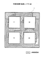
図1は、半導体装置1の配線のレイアウトを示す概念図である。半導体装置1に回路ブロック11乃至14が配置されるものとして、回路ブロック11乃至14間を信号配線で結線した様子を示している。
FIG. 1 is a conceptual diagram showing a wiring layout of the
半導体装置1に配置される個々の回路ブロック11乃至14に入出力される信号の種類や信号数、または/および回路ブロック11乃至14における信号の接続端子位置は、回路ブロック11乃至14に応じて変わるものである。また、回路ブロック11乃至14の配置位置に応じて信号配線のレイアウトも異なるものとなる。
The type and number of signals input / output to / from the
信号配線は、回路ブロック11乃至14間にある領域にレイアウトされることとなるが、回路ブロック11乃至14の回路構成や信号配線の接続端子位置は回路ブロックごとに固有であり、半導体装置1における回路ブロック11乃至14のレイアウト位置も選択可能である。このため、配置された回路ブロック11乃至14間を結線する信号配線のレイアウトは、配置された回路ブロック11乃至14とその配置位置に大きく依存することとなる。回路ブロック間の領域において、信号配線の密なる領域と粗なる領域とが混在することとなる。更に言えば、必要となる信号配線の結線位置に応じて、回路ブロック間の領域内に信号配線がレイアウトされていない未配線領域Xが点在することとなる。未配線領域Xは、信号配線のレイアウトに応じて無作為の位置に点在して存在し、各々の未配線領域Xの大きさも異なったものとなる。
The signal wiring is laid out in a region between the
ここで、未配線領域Xとは、信号配線が存在せず積層される配線層が信号配線としては未使用である領域のほか、一部の配線層を信号配線として使用しているものの、積層される配線層のうち連続する2層以上の配線層が信号配線としては未使用である領域を含むものとする。これにより、信号配線としては未使用であって隣接して積層される配線層を対として容量素子を構成することができる。 Here, the unwired region X is a region in which a part of a wiring layer is used as a signal wiring in addition to a region where a wiring layer laminated without a signal wiring is not used as a signal wiring. It is assumed that two or more continuous wiring layers among the wiring layers to be included include regions that are not used as signal wirings. As a result, a capacitive element can be configured by using a pair of wiring layers that are unused as signal wirings and are stacked adjacent to each other.
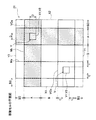
図2および図3に、実施形態の容量セル21を示す。図2に斜視図を示し、図3に平面図を示す。図3の平面図においては、レイアウト上のデザインルールを示す。
2 and 3 show the
容量セル21は、多層に積層される金属配線層のうち隣接して積層される配線層Ma、Mbを1対の電極層T1、T2として構成されている。各電極層T1、T2は、対応する配線層Ma、Mbが平面方向を区画する4つの横端面X1、X2、Y1、Y2のうち、対向する横端面X1、X2、および横端面Y1、Y2の各々に直交して、線幅Aで配線されている。この場合、配線層Ma、Mbは、線間の間隔として配線間隔Bを保ち、対向する横端面X1、X2、および横端面Y1、Y2に直交して配線される配線層Ma、Mbの交差領域が、図3に示す平面視において対角線上に位置して配線されている。電極層T1、T2の横端面X1、X2、Y1、Y2への接面が第2接続端子T12、T22である。容量セル21では、第2接続端子T12、T22の配置位置を3次元座標で指定すると、第2接続端子T12、T22の各々は、対向する横端面X1、X2、およびY1、Y2ごとに、同一平面座標に配置されている。また各電極層T1、T2に直接に接続されている。
The
直交して配線される配線層Ma、Mbの各々の交差領域には、縦方向経路を構成する線幅Dの第1ビアコンタクト層V1および第2ビアコンタクト層V2が接続される。ビアコンタクト層と配線層との接続点において、第1および第2ビアコンタクト層V1、V2から配線層Ma、Mbの端部までの接続余裕距離は線幅Cである。 A first via contact layer V1 and a second via contact layer V2 having a line width D constituting a vertical path are connected to the intersecting regions of the wiring layers Ma and Mb that are wired orthogonally. At the connection point between the via contact layer and the wiring layer, the connection margin distance from the first and second via contact layers V1 and V2 to the ends of the wiring layers Ma and Mb is the line width C.
第1ビアコンタクト層V1は、配線層Maと配線層Mbとを接続するビアコンタクト層である。配線層Ma、Mbから、対をなす配線層Mb、Maに向かって備えられ、配線層Mb、Maで構成されるビア接続層VCb、VCaに接続される。ビア接続層VCa、VCbも配線層Ma、Mbで構成されるので、線幅Aの線幅を有し、接続点において、第1ビアコンタクト層V1から端部までの接続余裕距離は線幅Cで構成される。 The first via contact layer V1 is a via contact layer that connects the wiring layer Ma and the wiring layer Mb. The wiring layers Ma and Mb are provided from the wiring layers Ma and Mb toward the wiring layers Mb and Ma that form a pair, and are connected to the via connection layers VCb and VCa configured by the wiring layers Mb and Ma. Since the via connection layers VCa and VCb are also composed of the wiring layers Ma and Mb, the via connection layers VCa and VCb have the line width A, and the connection margin distance from the first via contact layer V1 to the end at the connection point is the line width C. Consists of.
第2ビアコンタクト層V2は、配線層Maから下端面Z1を越え、配線層Mbから上端面Z2を越えて、容量セル21の外方にある配線層(不図示)に接続する際のビアコンタクト層である。容量セル21に備えられている第2ビアコンタクト層V2は、上下方向に容量セル21が連結されることから、配線層間の層間距離の略1/2の長さを有して第1接続端子T11、T21に接続されている。電極層T1およびビア接続層VCaを構成する配線層Maから下端面Z1に直交して下方に備えられ、また電極層T2およびビア接続層VCbを構成する配線層Mbから上端面Z2に直交して上方に備えられる。接続点において、第2ビアコンタクト層V2からビア接続層VCa、VCbの端部までの接続余裕距離は線幅Cである。第2ビアコンタクト層V2の下端面Z1および上端面Z2への接面が第1接続端子T11、T21である。容量セル21では、第1接続端子T11、T21の配置位置を3次元座標で指定すると、第1接続端子T11、T21の各々は、対向する下端面Z1および上端面Z2で、同一座標に配置されている。また、第2ビアコンタクト層V2は第1ビアコンタクト層V1と平面視で同じ位置に配置されている。第1ビアコンタクト層V1と同様にビア接続層VCa、VCbに接続されるためである。
The second via contact layer V2 extends from the wiring layer Ma to the lower end surface Z1 and from the wiring layer Mb to the upper end surface Z2 to connect to a wiring layer (not shown) outside the
なお、図3に示すように、配線層Ma、Mbから各横端面X1,X2,Y1,Y2までの距離は、配線間隔Bの略半分である。これにより、横端面X1、X2、Y1、Y2で容量セル21を連結する場合に、配線層Ma、Mbの線間距離が配線間隔Bとなる。
As shown in FIG. 3, the distances from the wiring layers Ma and Mb to the lateral end surfaces X1, X2, Y1, and Y2 are substantially half of the wiring interval B. Thereby, when the
ここで、線幅A、C,D、および配線間隔Bについては、各々の配線層Ma、Mb、第1および第2ビアコンタクト層V1、V2に対して定められているデザインルールに従って決定される。配線層間で同じデザインルールが適用される場合には、許容される最小値で構成することで最小サイズの容量セル21を構成することができる。最小許容値で構成することにより、容量セルの占有面積が低減され未配線領域Xに効率よく配置することができると共に、単位面積あたりの容量値の増大を図ることができる。残存する未配線領域Xに有効に配置して、小さな占有面積で大きな容量値を有する容量素子を構成することができる。
Here, the line widths A, C, D, and the wiring interval B are determined according to the design rules defined for the respective wiring layers Ma, Mb, the first and second via contact layers V1, V2. . When the same design rule is applied between the wiring layers, the
また、配線層間でデザインルールが異なる場合には、図4に示すように、配線層ごとの許容最小サイズのうち最大値で構成することにより、デザインルールの異なる配線層間に対しても、ビアコンタクト層V34、V45、V56、V67、V78、V89の配置位置を合わせることができる。積層される多層配線層の深さ方向に対して同じ平面状の面積を有して容量セルを接続することができる。 In addition, when the design rule differs between the wiring layers, as shown in FIG. 4, by using the maximum value among the minimum allowable sizes for each wiring layer, via contacts can also be made between the wiring layers with different design rules. The arrangement positions of the layers V34, V45, V56, V67, V78, and V89 can be matched. Capacitance cells can be connected with the same planar area with respect to the depth direction of the multilayer wiring layers to be stacked.
図4について説明する。最下層の金属配線層M4、M5およびビアコンタクト層V34、V45は、レイアウトの際のデザインルールが最小の許容値まで許されている。その上に積層される金属配線層M6、M7およびビアコンタクト層V56、V67は、最下層に比して大きな最小許容値を有するデザインルールでレイアウトすることが許されている。更に上層の金属配線層M8、M9およびビアコンタクト層V78、V89については、更に大きな最小許容値のデザインルールが許されている。各々隣接する2層の金属配線層で容量セルを構成する場合、各々の層で最小許容値のデザインルールを使用してレイアウトしてしまうと、最小許容値が異なる層間で第1接続端子のピッチが合わず、容量セルを縦方向に連結することはできない(図4中、(A)の場合)。そこで、最小許容値を、容量素子として使用する可能性がある最上層のデザインルールで統一してやれば、層間の第1接続端子のピッチを統一することができ、容量セルを縦方向で直結することができる(図4中、(B)の場合)。 FIG. 4 will be described. The lowermost metal wiring layers M4 and M5 and the via contact layers V34 and V45 are allowed up to a minimum allowable value in the design rule at the time of layout. The metal wiring layers M6 and M7 and the via contact layers V56 and V67 laminated thereon are allowed to be laid out with a design rule having a large minimum allowable value as compared with the lowermost layer. Further, for the upper metal wiring layers M8 and M9 and the via contact layers V78 and V89, a design rule with a larger minimum allowable value is allowed. When a capacitor cell is composed of two adjacent metal wiring layers, if the layout is made using the design rule with the minimum allowable value in each layer, the pitch of the first connection terminals between the layers having different minimum allowable values And the capacity cells cannot be connected vertically (in the case of (A) in FIG. 4). Therefore, if the minimum allowable value is unified with the design rule of the uppermost layer that may be used as a capacitor element, the pitch of the first connection terminals between the layers can be unified, and the capacitor cells are directly connected in the vertical direction. (In the case of (B) in FIG. 4).
また、図4では、隣接する2層の金属配線層ごとに許容最小値のデザインルールが異なる場合を例にとり説明したが、隣接する4層以上の金属配線層において同一のデザインルールが適用される場合がある。2対以上の容量セルを構成することができる複数層の金属配線層で、同一のデザインルールが適用される場合である。この場合には、同一のデザインルールを有する金属配線層でグループ化し、グループごとに対応するデザインルールに適合した最小許容値で容量セルを構成することも考えられる。 In FIG. 4, the case where the design rule of the allowable minimum value is different for each of two adjacent metal wiring layers has been described as an example. However, the same design rule is applied to four or more adjacent metal wiring layers. There is a case. This is a case where the same design rule is applied to a plurality of metal wiring layers that can form two or more pairs of capacity cells. In this case, it is conceivable to group the metal wiring layers having the same design rule, and configure the capacity cell with the minimum allowable value that conforms to the design rule corresponding to each group.
図5は、容量セル21の連結を示す図である。容量セル21は、電極層T1、T2ごとに、対向する端面で同一の平面座標に第1接続端子T11、T21および第2接続端子T12、T22が配置されているので、2つの容量セル21を同じ向きに直結してやれば、それぞれの電極層T1、T2が連結される。
FIG. 5 is a diagram showing the connection of the
上下方向に連結される場合は、下端面Z1と上端面Z2とが接合される。下端面Z1の第1接続端子T11と上端面Z2の第1接続端子T11が連結され、下端面Z1の第1接続端子T21と上端面Z2の第1接続端子T21が連結される。 When connected in the vertical direction, the lower end surface Z1 and the upper end surface Z2 are joined. The first connection terminal T11 on the lower end surface Z1 and the first connection terminal T11 on the upper end surface Z2 are coupled, and the first connection terminal T21 on the lower end surface Z1 and the first connection terminal T21 on the upper end surface Z2 are coupled.
平面方向に連結される場合は、横端面X1と横端面X2、および横端面Y1と横端面Y2とが接合される。横端面X1の第2接続端子T12と横端面X2の第2接続端子T12が連結され、横端面X1の第2接続端子T22と横端面X2の第2接続端子T22が連結される。また、横端面Y1の第2接続端子T12と横端面Y2の第2接続端子T12が連結され、横端面Y1の第2接続端子T22と横端面Y2の第2接続端子T22が連結される。 When coupled in the planar direction, the lateral end surface X1 and the lateral end surface X2 and the lateral end surface Y1 and the lateral end surface Y2 are joined. The second connection terminal T12 on the lateral end surface X1 and the second connection terminal T12 on the lateral end surface X2 are coupled, and the second connection terminal T22 on the lateral end surface X1 and the second connection terminal T22 on the lateral end surface X2 are coupled. Further, the second connection terminal T12 on the lateral end surface Y1 and the second connection terminal T12 on the lateral end surface Y2 are coupled, and the second connection terminal T22 on the lateral end surface Y1 and the second connection terminal T22 on the lateral end surface Y2 are coupled.
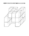
図6、図7に容量セル21を連結して容量素子を構成する場合を例示する。図6は2次元に連結した場合である。横端面X1と横端面X2、および横端面Y1と横端面Y2で容量セル21を連結して、4セル×4セルの容量素子が構成されている。容量セル21では、横端面X1、X2、Y1、Y2と各配線層Ma、Mbの端辺との距離が、配線間隔Bの略半分(B/2)で構成されている。このため、容量セル21を横方向に連結した際、隣接間における配線層Ma、Mb間の線間距離が、デザインルール上の許容最小値である配線間隔Bとなる。具体的には、電極層T1が許容最小間隔でビア接続層VCaを取り巻き、および電極層T2が許容最小間隔でビア接続層VCbを取り巻く。上下方向においては、電極層T1、T2間で容量部を構成する。加えて平面方向においては、電極層T1とビア接続層VCa、および電極層T2とビア接続層VCbとが、許容最小値の間隔で容量部を構成し、単位面積当たりの容量値を大きくすることに寄与している。容量セル21を2次元に連結して容量素子を構成する場合に、平面方向における単位あたりの容量値を大きくすることができる。効率よく大容量の容量素子を構成することができる。
FIG. 6 and FIG. 7 illustrate the case where the capacitive element is configured by connecting the
図7は3次元に連結した場合である。図6の容量素子を上下方向に3段に連結した構成を有している。上下方向においては、隣接する容量セル21を連結する第1および第2ビアコンタクト層V1、V2により、隣接容量セル21間で、各電極層T1、T2が電極層ごとに連結され、対をなす電極層を取り囲むように構成される。電極層T1と第1および第2ビアコンタクト層V1、V2とが、電極層T2を取り囲み、電極層T2と第1および第2ビアコンタクト層V1、V2とが、電極層T1を取り囲む。これにより、平面方向に加えて、上下方向においても単位面積あたりの容量値が大きくとれ効率的な容量素子を構成することができる。
FIG. 7 shows a case where three dimensions are connected. 6 has a configuration in which the capacitive elements are connected in three stages in the vertical direction. In the vertical direction, the first and second via contact layers V1 and V2 connecting the
図8は、図1に示した任意形状の未配線領域Xに、有効に容量素子を構成する場合を模式的に示す図である。未配線領域Xの形状は、平面方向において任意の形状となることに加えて、上下方向においても任意の形状になる場合が考えられる。信号配線の平面方向の有無の違いに加えて、多層配線構造を有する半導体装置1の場合には、信号配線に使用される配線層の違いに応じて上下方向にも信号配線の有無の違いがあるからである。
FIG. 8 is a diagram schematically showing a case where a capacitive element is effectively formed in the unshaped wiring region X having an arbitrary shape shown in FIG. The shape of the unwired region X may be an arbitrary shape in the vertical direction in addition to an arbitrary shape in the planar direction. In the case of the
3次元的に任意の形状を有する未配線領域Xを容量素子の配置領域として有効に使用するために、容量セル21を利用することができる。図8にある直方体は容量セル21を示す。容量セル21は上下方向および平面方向に自由に連結できる。これにより、未配線領域Xの3次元的な形状に合わせて容量セル21を連結することができ、未配線領域Xを有効に使用した容量素子を構成することができる。
In order to effectively use the unwired region X having an arbitrary shape three-dimensionally as a capacitor element placement region, the
図9に示す容量セル22は容量セル21の変形例である。容量セル21では、第1接続端子T11、T21には、上下端面Z2、Z1共に、第2ビアコンタクト層V2が接続される。このときの第2ビアコンタクト層V2の長さは、第2ビアコンタクト層V2で接続される配線層間の層間距離の略半分である。これに対して容量セル22では、上下端面Z2、Z1のうち何れか一方の端面にある第1接続端子T11、T21には、第2ビアコンタクト層V2に代えて、電極層T1またはT2、およびビア接続層VCaまたはVCbが接続される。また他方の端面にある第1接続端子T11、T21に接続される第2ビアコンタクト層V2の長さは、配線層間の層間距離である。
A
電極層T1およびビア接続層VCaが下端面Z1の第1接続端子T11、T21に接続される場合は、容量セルを連結して容量素子を構成する場合の最下段のセルとして容量セル22を使用することができる。最下層の配線層を配線層Maとして容量素子を構成することができる。電極層T2およびビア接続層VCbが上端面Z2の第1接続端子T21、T11に接続される場合は、容量セルを連結して容量素子を構成する場合の最上段のセルとして容量セル22を使用することができる。最上層の配線層を配線層Mbとして容量素子を構成することができる。
When the electrode layer T1 and the via connection layer VCa are connected to the first connection terminals T11 and T21 on the lower end surface Z1, the
以上詳細に説明したとおり、本実施形態に係る容量セル、半導体装置、および容量素子の配置方法によれば、1対の電極層T1、T2を備え、各電極層T1、T2に接続される第1および第2接続端子T11、T21およびT12、T22を容量セル21、22の境界面である上/下端面Z2/Z1および横端面X1、X2、Y1、Y2にそれぞれ備えているので、容量セル21、22を互いに連結してやれば、容量セル21、22の単位で、素子サイズや容量値等が増減可能な容量素子を構成することができる。
As described above in detail, according to the arrangement method of the capacitive cell, the semiconductor device, and the capacitive element according to the present embodiment, the first electrode layer T1, T2 is provided and is connected to each electrode layer T1, T2. Since the first and second connection terminals T11, T21, T12, and T22 are provided on the upper / lower end surface Z2 / Z1 and the lateral end surfaces X1, X2, Y1, and Y2 that are the boundary surfaces of the
容量セル21、22の大きさを信号配線の後に残存する未配線領域Xに配置可能な大きさに設定してやれば、信号配線により生ずる未配線領域Xの大きさ、上下および平面方向の形状等に関わらず、容量セル21、22を必要に応じて連結して容量素子を構成することができる。信号が配線されていない空き領域を有効に活用して容量素子を配置することができる。信号配線領域とは別に容量配線領域を確保することは不要であり、容量素子を配置する際に高集積化に資するところ大である。
If the size of the
尚、本発明は前記実施形態に限定されるものではなく、本発明の趣旨を逸脱しない範囲内で種々の改良、変形が可能であることは言うまでもない。
例えば、本実施形態においては、第1接続端子T11、T21、および第2接続端子T12、T22を、対向する端面において同一位置に配置されるものとして説明したが、本発明はこれに限定されるものではなく、対向する端面間で異なる位置に配置することも可能である。この場合、容量セルを鏡面対象にして折り返すことにより連結することができる。
また、容量セル21、22では、電極層T1、T2がセル内において直交する場合を例にとり説明したが、本発明はこれに限定されるものではない。1対の配線層を1対の電極層として有し、上下方向および平面方向の各端面において、電極層ごとに、外部との接続を可能とする構成とすれば、レイアウト形状に制約はない。例えば、電極層T1、T2を上下方向に重なりを有し一つの横端面に沿って並走させるように配置し、ビアコンタクト層を、電極層T1、T2に並走する横端面に対向する横端面に並べて配置する構成とすることもできる。
The present invention is not limited to the above-described embodiment, and it goes without saying that various improvements and modifications can be made without departing from the spirit of the present invention.
For example, in the present embodiment, the first connection terminals T11 and T21 and the second connection terminals T12 and T22 have been described as being disposed at the same position on the opposing end surfaces, but the present invention is limited to this. It is also possible to arrange them at different positions between the opposed end faces. In this case, the capacity cells can be connected by folding them back as mirror surfaces.
Further, in the
ここで、本発明の技術思想により、背景技術における課題を解決するための手段を以下に列記する。
(付記1) 多層に積層される配線層を電極とする容量セルであって、
隣接して積層される1対の配線層により構成される1対の電極層と、
前記電極層ごとに、上下方向を区画する上端面および下端面に備えられ、該電極層に接続される第1接続端子と、
前記電極層ごとに、平面方向を区画する4つの横端面に備えられ、該電極層に接続される第2接続端子と
を備えることを特徴とする容量セル。
(付記2) 前記電極層を構成する配線層は金属配線層であり、前記電極層と前記第1接続端子とを接続する縦方向経路は、ビアコンタクト層を含んで構成されることを特徴とする付記1に記載の容量セル。
(付記3) 前記縦方向経路のうち、該縦方向経路が接続されている前記電極層に対して対をなす前記電極層の配置側にある経路は、
前記1対の配線層を接続する第1ビアコンタクト層と、
前記第1ビアコンタクト層に接続され、対をなす前記電極層と同じ配線層により構成されるビア接続層と
を備えることを特徴とする付記2に記載の容量セル。
(付記4) 前記縦方向経路のうち、前記上端面または前記下端面の少なくとも何れか一方の端面にある前記第1接続端子に接続される経路は、更に、
前記電極層および前記ビア接続層を構成する前記配線層と、前記第1接続端子の外方にある配線層とを接続する第2ビアコンタクト層を備えることを特徴とする付記3に記載の容量セル。
(付記5) 前記第2ビアコンタクト層が前記上端面および前記下端面の双方に備えられる場合、
該第2ビアコンタクト層の経路長は、前記第2ビアコンタクト層により接続される前記配線層間の層間距離の略半分の長さであることを特徴とする付記4に記載の容量セル。
(付記6) 前記第2ビアコンタクト層が前記上端面および前記下端面の何れか一方に備えられる場合、
前記上端面または前記下端面の一方にある前記第1接続端子は、前記第2ビアコンタクト層に接続され、
前記上端面または前記下端面の他方にある前記第1接続端子は、前記電極層または前記ビア接続層に接続されることを特徴とする付記4に記載の容量セル。
(付記7) 前記第1接続端子は、配置位置を3次元座標により指定する場合、前記電極層ごとに、前記上端面内の平面座標と前記下端面内の平面座標とが、同一座標を有して配置されていることを特徴とする付記1に記載の容量セル。
(付記8) 前記第2接続端子は、配置位置を3次元座標により指定する場合、前記電極層ごとに、対向する前記横端面内の平面座標が同一座標を有して配置されていることを特徴とする付記1に記載の容量セル。
(付記9) 各々の前記電極層は、前記1対の配線層のうち一つの配線層で構成され、該配線層は、4つの前記横端面にある前記第2接続端子に接続されることを特徴とする付記1に記載の容量セル。
(付記10) 多層に積層される前記配線層のうち最大のデザインルールによりレイアウトされることを特徴とする付記1に記載の容量セル。
(付記11) 付記1乃至10の少なくともいずれか一項に記載の容量セルが、少なくとも2つ連結されて構成される容量素子を備えることを特徴とする半導体装置。
(付記12) 前記容量セルの連結は、上下方向においては前記第1接続端子の連結により行なわれ、平面方向においては前記第2接続端子の連結により行なわれることを特徴とする付記11に記載の半導体装置。
(付記13) 最上段および最下段に連結される容量セルは付記6に記載の容量セルであり、
最上段に連結される場合は、前記下端面にある前記第1接続端子が前記第2ビアコンタクト層に接続されると共に、前記上端面にある前記第1接続端子が前記電極層または前記ビア接続層に接続され、
最下段に連結される場合には、前記上端面にある前記第1接続端子が前記第2ビアコンタクト層に接続されると共に、前記下端面にある前記第1接続端子が前記電極層または前記ビア接続層に接続されることを特徴とする付記12に記載の半導体装置。
(付記14) 付記7または8の少なくとも何れか一項に記載の容量セルが連結される場合、
前記容量セルは同じ向きであって、対向する端面間距離を連結する際の配置ピッチとして連結されることを特徴とする付記11に記載の半導体装置。
(付記15) 多層に積層される配線層を電極とする容量セルの配置方法であって、
隣接して積層される1対の配線層を1対の電極層とし、上下および平面方向に区画されると共に、前記上下および平面方向の各端面において、外部から前記電極層の各々に接続可能な容量セルを準備するステップと、
前記容量セルを少なくとも2つ連結して容量素子を構成するステップと
を有することを特徴とする容量素子の配置方法。
(付記16) 前記容量素子を準備するステップでは、外部から前記電極層への接続位置は、前記電極層ごとに、前記上下および平面方向の各端面のうち対向する端面において、面内の同一位置とされ、
前記連結のステップでは、前記容量セルは同じ向きであって、対向する端面間距離を連結する際の配置ピッチとされることを特徴とする付記15に記載の容量素子の配置方法。
Here, the means for solving the problems in the background art according to the technical idea of the present invention are listed below.
(Additional remark 1) It is a capacity | capacitance cell which uses the wiring layer laminated | stacked in a multilayer as an electrode,
A pair of electrode layers constituted by a pair of wiring layers stacked adjacent to each other;
For each of the electrode layers, a first connection terminal provided on an upper end surface and a lower end surface that divides the vertical direction and connected to the electrode layer;
Each of the electrode layers includes a second connection terminal that is provided on four lateral end surfaces that define a planar direction and is connected to the electrode layer.
(Additional remark 2) The wiring layer which comprises the said electrode layer is a metal wiring layer, The vertical direction path | route which connects the said electrode layer and the said 1st connection terminal is comprised including a via contact layer, It is characterized by the above-mentioned. The capacity cell according to
(Supplementary Note 3) Of the vertical paths, the path on the arrangement side of the electrode layer that is paired with the electrode layer to which the vertical path is connected is:
A first via contact layer connecting the pair of wiring layers;
The capacitor cell according to
(Additional remark 4) The path | route connected to the said 1st connection terminal in at least any one end surface of the said upper end surface or the said lower end surface among the said vertical direction path | route further,
The capacitor according to claim 3, further comprising: a second via contact layer that connects the wiring layer constituting the electrode layer and the via connection layer and a wiring layer outside the first connection terminal. cell.
(Supplementary Note 5) When the second via contact layer is provided on both the upper end surface and the lower end surface,
The capacity cell according to appendix 4, wherein the path length of the second via contact layer is approximately half the distance between the wiring layers connected by the second via contact layer.
(Supplementary Note 6) When the second via contact layer is provided on either the upper end surface or the lower end surface,
The first connection terminal on one of the upper end surface or the lower end surface is connected to the second via contact layer,
The capacity cell according to appendix 4, wherein the first connection terminal on the other of the upper end surface or the lower end surface is connected to the electrode layer or the via connection layer.
(Supplementary Note 7) When the arrangement position is designated by a three-dimensional coordinate, the first connection terminal has the same coordinate for each electrode layer in the plane coordinate in the upper end surface and the plane coordinate in the lower end surface. The capacity cell according to
(Supplementary Note 8) The second connecting terminal, to specify the three-dimensional coordinates position, for each of the electrode layers, that plane coordinates of the lateral end plane facing is arranged with the same coordinate The capacity cell according to
(Additional remark 9) Each said electrode layer is comprised by one wiring layer among said one pair of wiring layers, and this wiring layer is connected to the said 2nd connection terminal in the said 4 said horizontal end surface. The capacity cell according to
(Supplementary note 10) The capacity cell according to
(Additional remark 11) The semiconductor device characterized by including the capacitive element comprised by connecting at least 2 capacity | capacitance cells as described in any one of
(Additional remark 12) Connection of the said capacity cell is performed by the connection of the said 1st connection terminal in an up-down direction, and is performed by the connection of the said 2nd connection terminal in a plane direction. Semiconductor device.
(Supplementary Note 13) The capacity cells connected to the uppermost and lowermost stages are the capacity cells described in Supplementary Note 6.
When connected to the uppermost stage, the first connection terminal on the lower end surface is connected to the second via contact layer, and the first connection terminal on the upper end surface is connected to the electrode layer or the via connection. Connected to the layers,
When connected to the lowermost stage, the first connection terminal on the upper end surface is connected to the second via contact layer, and the first connection terminal on the lower end surface is connected to the electrode layer or the via.
(Supplementary note 14) When the capacity cell according to any one of Supplementary notes 7 and 8 is connected,
12. The semiconductor device according to
(Additional remark 15) It is the arrangement | positioning method of the capacity | capacitance cell which uses the wiring layer laminated | stacked in a multilayer as an electrode,
A pair of wiring layers stacked adjacent to each other is used as a pair of electrode layers, which are partitioned in the vertical and planar directions and can be connected to each of the electrode layers from the outside at each of the end surfaces in the vertical and planar directions. Preparing a capacity cell;
And a step of connecting at least two of the capacity cells to form a capacity element.
(Supplementary Note 16) In the step of preparing the capacitive element, the connection position from the outside to the electrode layer is the same in-plane position on each of the electrode layers at the opposing end surfaces of the upper and lower and planar surfaces. And
16. The method of arranging a capacitive element according to appendix 15, wherein in the connecting step, the capacitor cells are in the same direction, and the pitch between the opposing end faces is set as an arrangement pitch.
1 半導体装置
11乃至14 回路ブロック
21、22 容量セル
M4、M5、M6、M7、M8、M9 金属配線層
Ma、Mb 配線層
T1、T2 電極層
T11、T21 第1接続端子
T12、T22 第2接続端子
V1 第1ビアコンタクト層
V2 第2ビアコンタクト層
V34、V45、V56、V67、V78、V89 ビアコンタクト層
VCa、VCb ビア接続層
X 未配線領域
X1、X2、Y1、Y2 横端面
Z1 下端面
Z2 上端面
DESCRIPTION OF
Claims (5)
前記第一の配線層に隣接する第二の配線層に形成され、交差する第三配線と第四配線からなる第二電極と、
前記第一の配線層に形成され、前記第一、第二の配線層間を接続するための第一ビアコンタクト層を介して前記第三、第四配線の交差領域と接続される第一ビア接続部と、
前記第二の配線層に形成され、前記第一ビアコンタクト層を介して前記第一、第二配線の交差領域と接続される第二ビア接続部とを備え、
前記第三、第四配線の交差領域と前記第一、第二配線の交差領域、および前記第一ビア接続部と前記第二ビア接続部とは、おのおの対角上に位置され、
前記第一ビア接続部と前記第一、第二配線との間、および前記第二ビア接続部と前記第三、第四配線との間は第一配線間隔だけ離間し、
前記第一、第二配線は、前記第一、第二の配線層の積層面と直交する方向の前記第二電極の配線方向外方の端面、および前記第一、第二の配線層の積層面と直交する方向の前記第一電極の配線方向外方の端面から、前記第一配線間隔の半分の長さだけ外方に突出して形成され、
前記第三、第四配線は、前記第一、第二の配線層の積層面と直交する方向の前記第一電極の配線方向外方の端面、および前記第一、第二の配線層の積層面と直交する方向の前記第二電極の配線方向外方の端面から、前記第一配線間隔の半分の長さだけ外方に突出して形成されることを特徴とする容量セル。 A first electrode made of a first wiring and a second wiring formed in the first wiring layer and intersecting;
Formed in a second wiring layer adjacent to the first wiring layer, a second electrode comprising a third wiring and a fourth wiring intersecting each other;
A first via connection formed in the first wiring layer and connected to an intersecting region of the third and fourth wirings via a first via contact layer for connecting the first and second wiring layers. And
A second via connection portion formed in the second wiring layer and connected to an intersection region of the first and second wirings via the first via contact layer;
The intersecting region of the third and fourth wirings and the intersecting region of the first and second wirings, and the first via connection part and the second via connection part are respectively positioned diagonally,
The first via connection portion and the first and second wiring, and the second via connection portion and the third and fourth wiring are separated by a first wiring interval,
The first and second wirings are the end surfaces of the second electrodes in the wiring direction outward in the direction orthogonal to the stacked surfaces of the first and second wiring layers, and the stacked layers of the first and second wiring layers. Formed from the outer end surface of the first electrode in the direction orthogonal to the surface outwardly by the length of half of the first wiring interval,
The third and fourth wirings are the end surfaces of the first electrodes in the direction perpendicular to the stacked surfaces of the first and second wiring layers, and the stacked layers of the first and second wiring layers. A capacitor cell, characterized in that it is formed to project outward from the end surface of the second electrode in the direction orthogonal to the surface in the wiring direction outward by a half length of the first wiring interval.
第一容量セルとして請求項2に記載の容量セルを有し、
第二容量セルとして請求項2に記載の容量セルを有し、
前記第一容量セルと前記第二容量セルとは、第一および第三配線を介して接続され、あるいは第二および第四配線を介して接続されることを特徴とする容量。 Capacity,
It has the capacity cell according to claim 2 as a first capacity cell,
It has a capacity cell according to claim 2 as a second capacity cell,
The first capacity cell and the second capacity cell are connected via a first and third wiring, or are connected via a second and fourth wiring.
Priority Applications (2)
| Application Number | Priority Date | Filing Date | Title |
|---|---|---|---|
| JP2006036376A JP5259054B2 (en) | 2006-02-14 | 2006-02-14 | Capacity cell, and capacity |
| US11/482,012 US7872293B2 (en) | 2006-02-14 | 2006-07-07 | Capacitance cell, semiconductor device, and capacitance cell arranging method |
Applications Claiming Priority (1)
| Application Number | Priority Date | Filing Date | Title |
|---|---|---|---|
| JP2006036376A JP5259054B2 (en) | 2006-02-14 | 2006-02-14 | Capacity cell, and capacity |
Publications (2)
| Publication Number | Publication Date |
|---|---|
| JP2007220716A JP2007220716A (en) | 2007-08-30 |
| JP5259054B2 true JP5259054B2 (en) | 2013-08-07 |
Family
ID=38367486
Family Applications (1)
| Application Number | Title | Priority Date | Filing Date |
|---|---|---|---|
| JP2006036376A Expired - Fee Related JP5259054B2 (en) | 2006-02-14 | 2006-02-14 | Capacity cell, and capacity |
Country Status (2)
| Country | Link |
|---|---|
| US (1) | US7872293B2 (en) |
| JP (1) | JP5259054B2 (en) |
Families Citing this family (3)
| Publication number | Priority date | Publication date | Assignee | Title |
|---|---|---|---|---|
| US5486228A (en) | 1992-07-31 | 1996-01-23 | Binney & Smith Inc. | Washable color changing compositions |
| US5498282A (en) | 1992-07-31 | 1996-03-12 | Binney & Smith Inc. | Color changing pan paint compositions |
| CN103125020B (en) * | 2010-09-29 | 2016-01-20 | 意法爱立信有限公司 | There is the power-supply wiring of integrated decoupling capacitor |
Family Cites Families (11)
| Publication number | Priority date | Publication date | Assignee | Title |
|---|---|---|---|---|
| JPH11204372A (en) * | 1997-11-14 | 1999-07-30 | Murata Mfg Co Ltd | Monolithic capacitor |
| JP2001177056A (en) | 1999-12-16 | 2001-06-29 | Hitachi Ltd | Semiconductor integrated circuit device |
| US6690570B2 (en) * | 2000-09-14 | 2004-02-10 | California Institute Of Technology | Highly efficient capacitor structures with enhanced matching properties |
| JP2002299555A (en) * | 2001-03-30 | 2002-10-11 | Seiko Epson Corp | Integrated circuit and manufacturing method thereof |
| JP2003249559A (en) | 2002-02-22 | 2003-09-05 | Handotai Rikougaku Kenkyu Center:Kk | Multilayer wiring apparatus, wiring method, and wiring characteristic analysis / prediction method |
| JP4112244B2 (en) * | 2002-03-04 | 2008-07-02 | 富士通株式会社 | Semiconductor integrated circuit element design system, program, recording medium, and semiconductor integrated circuit element design method |
| DE10217565A1 (en) * | 2002-04-19 | 2003-11-13 | Infineon Technologies Ag | Semiconductor component with an integrated grid-shaped capacitance structure |
| JP2004241762A (en) | 2003-01-16 | 2004-08-26 | Nec Electronics Corp | Semiconductor device |
| US6952338B1 (en) * | 2003-11-07 | 2005-10-04 | Sony Corporation | Common pole capacitor housing apparatus and method |
| JP4525965B2 (en) * | 2004-01-06 | 2010-08-18 | ルネサスエレクトロニクス株式会社 | Semiconductor device |
| JP2006179620A (en) * | 2004-12-21 | 2006-07-06 | Sharp Corp | Semiconductor integrated circuit |
-
2006
- 2006-02-14 JP JP2006036376A patent/JP5259054B2/en not_active Expired - Fee Related
- 2006-07-07 US US11/482,012 patent/US7872293B2/en not_active Expired - Fee Related
Also Published As
| Publication number | Publication date |
|---|---|
| US20070187740A1 (en) | 2007-08-16 |
| JP2007220716A (en) | 2007-08-30 |
| US7872293B2 (en) | 2011-01-18 |
Similar Documents
| Publication | Publication Date | Title |
|---|---|---|
| JP4343085B2 (en) | Semiconductor device | |
| US7038296B2 (en) | Electrical component structure | |
| US8114752B2 (en) | Structure of capacitor set | |
| JP2004502315A (en) | Ceramic multilayer capacitor array | |
| US7646583B2 (en) | Common centroid symmetric structure capacitor | |
| JP2008112974A (en) | Semiconductor capacitor | |
| US6916996B2 (en) | Symmetric electrical connection system | |
| KR20010014709A (en) | Layered capacitor device | |
| JP5259054B2 (en) | Capacity cell, and capacity | |
| US9929084B2 (en) | Device with interconnection structure for forming a conduction path or a conducting plane with high decoupling capacitance | |
| JP5433972B2 (en) | Semiconductor device and manufacturing method thereof | |
| JP2009245961A (en) | Semiconductor integrated circuit | |
| CN114450792A (en) | Laminated semiconductor, wafer laminated body, method for manufacturing laminated semiconductor, assist device, and program | |
| JP5774544B2 (en) | Capacitor structure | |
| JP2007059814A (en) | Multilayer capacitor | |
| TWI831224B (en) | Metal-oxide-metal capacitor structure | |
| JP2009252806A (en) | Semiconductor device, and its layout method | |
| CN100578785C (en) | Integrated circuit with multi-terminal capacitor | |
| JP2002100732A (en) | Capacitor element formation method | |
| JP2005032768A (en) | Semiconductor device | |
| CN101110417A (en) | Capacitor bank structure and method for reducing capacitance variation between capacitors | |
| CN111009514B (en) | Capacitor element unit for semiconductor device and semiconductor device thereof | |
| JP2006173418A (en) | Power supply structure of semiconductor integrated circuit | |
| CN116347972A (en) | Deep trench silicon capacitor and method of manufacturing the same | |
| JP2006059977A (en) | Composite capacitor |
Legal Events
| Date | Code | Title | Description |
|---|---|---|---|
| RD04 | Notification of resignation of power of attorney |
Free format text: JAPANESE INTERMEDIATE CODE: A7424 Effective date: 20070517 |
|
| RD03 | Notification of appointment of power of attorney |
Free format text: JAPANESE INTERMEDIATE CODE: A7423 Effective date: 20070521 |
|
| A711 | Notification of change in applicant |
Free format text: JAPANESE INTERMEDIATE CODE: A712 Effective date: 20080728 |
|
| A621 | Written request for application examination |
Free format text: JAPANESE INTERMEDIATE CODE: A621 Effective date: 20081008 |
|
| A131 | Notification of reasons for refusal |
Free format text: JAPANESE INTERMEDIATE CODE: A131 Effective date: 20111025 |
|
| A977 | Report on retrieval |
Free format text: JAPANESE INTERMEDIATE CODE: A971007 Effective date: 20111027 |
|
| A521 | Request for written amendment filed |
Free format text: JAPANESE INTERMEDIATE CODE: A523 Effective date: 20111222 |
|
| A02 | Decision of refusal |
Free format text: JAPANESE INTERMEDIATE CODE: A02 Effective date: 20120124 |
|
| A521 | Request for written amendment filed |
Free format text: JAPANESE INTERMEDIATE CODE: A523 Effective date: 20120418 |
|
| RD03 | Notification of appointment of power of attorney |
Free format text: JAPANESE INTERMEDIATE CODE: A7423 Effective date: 20120418 |
|
| A911 | Transfer to examiner for re-examination before appeal (zenchi) |
Free format text: JAPANESE INTERMEDIATE CODE: A911 Effective date: 20120425 |
|
| A912 | Re-examination (zenchi) completed and case transferred to appeal board |
Free format text: JAPANESE INTERMEDIATE CODE: A912 Effective date: 20120518 |
|
| A521 | Request for written amendment filed |
Free format text: JAPANESE INTERMEDIATE CODE: A523 Effective date: 20130307 |
|
| A61 | First payment of annual fees (during grant procedure) |
Free format text: JAPANESE INTERMEDIATE CODE: A61 Effective date: 20130424 |
|
| FPAY | Renewal fee payment (event date is renewal date of database) |
Free format text: PAYMENT UNTIL: 20160502 Year of fee payment: 3 |
|
| R150 | Certificate of patent or registration of utility model |
Ref document number: 5259054 Country of ref document: JP Free format text: JAPANESE INTERMEDIATE CODE: R150 |
|
| S111 | Request for change of ownership or part of ownership |
Free format text: JAPANESE INTERMEDIATE CODE: R313111 |
|
| R350 | Written notification of registration of transfer |
Free format text: JAPANESE INTERMEDIATE CODE: R350 |
|
| LAPS | Cancellation because of no payment of annual fees |