JP5258564B2 - Method for transferring a thin film onto a support - Google Patents
Method for transferring a thin film onto a support Download PDFInfo
- Publication number
- JP5258564B2 JP5258564B2 JP2008526524A JP2008526524A JP5258564B2 JP 5258564 B2 JP5258564 B2 JP 5258564B2 JP 2008526524 A JP2008526524 A JP 2008526524A JP 2008526524 A JP2008526524 A JP 2008526524A JP 5258564 B2 JP5258564 B2 JP 5258564B2
- Authority
- JP
- Japan
- Prior art keywords
- layer
- support
- germanium
- thin
- transfer method
- Prior art date
- Legal status (The legal status is an assumption and is not a legal conclusion. Google has not performed a legal analysis and makes no representation as to the accuracy of the status listed.)
- Expired - Fee Related
Links
Images

Classifications
-
- H—ELECTRICITY
- H10—SEMICONDUCTOR DEVICES; ELECTRIC SOLID-STATE DEVICES NOT OTHERWISE PROVIDED FOR
- H10P—GENERIC PROCESSES OR APPARATUS FOR THE MANUFACTURE OR TREATMENT OF DEVICES COVERED BY CLASS H10
- H10P90/00—Preparation of wafers not covered by a single main group of this subclass, e.g. wafer reinforcement
- H10P90/19—Preparing inhomogeneous wafers
- H10P90/1904—Preparing vertically inhomogeneous wafers
- H10P90/1906—Preparing SOI wafers
- H10P90/1914—Preparing SOI wafers using bonding
- H10P90/1916—Preparing SOI wafers using bonding with separation or delamination along an ion implanted layer, e.g. Smart-cut
-
- H—ELECTRICITY
- H10—SEMICONDUCTOR DEVICES; ELECTRIC SOLID-STATE DEVICES NOT OTHERWISE PROVIDED FOR
- H10W—GENERIC PACKAGES, INTERCONNECTIONS, CONNECTORS OR OTHER CONSTRUCTIONAL DETAILS OF DEVICES COVERED BY CLASS H10
- H10W10/00—Isolation regions in semiconductor bodies between components of integrated devices
- H10W10/10—Isolation regions comprising dielectric materials
- H10W10/181—Semiconductor-on-insulator [SOI] isolation regions, e.g. buried oxide regions of SOI wafers
-
- Y—GENERAL TAGGING OF NEW TECHNOLOGICAL DEVELOPMENTS; GENERAL TAGGING OF CROSS-SECTIONAL TECHNOLOGIES SPANNING OVER SEVERAL SECTIONS OF THE IPC; TECHNICAL SUBJECTS COVERED BY FORMER USPC CROSS-REFERENCE ART COLLECTIONS [XRACs] AND DIGESTS
- Y10—TECHNICAL SUBJECTS COVERED BY FORMER USPC
- Y10T—TECHNICAL SUBJECTS COVERED BY FORMER US CLASSIFICATION
- Y10T156/00—Adhesive bonding and miscellaneous chemical manufacture
- Y10T156/10—Methods of surface bonding and/or assembly therefor
- Y10T156/1052—Methods of surface bonding and/or assembly therefor with cutting, punching, tearing or severing
-
- Y—GENERAL TAGGING OF NEW TECHNOLOGICAL DEVELOPMENTS; GENERAL TAGGING OF CROSS-SECTIONAL TECHNOLOGIES SPANNING OVER SEVERAL SECTIONS OF THE IPC; TECHNICAL SUBJECTS COVERED BY FORMER USPC CROSS-REFERENCE ART COLLECTIONS [XRACs] AND DIGESTS
- Y10—TECHNICAL SUBJECTS COVERED BY FORMER USPC
- Y10T—TECHNICAL SUBJECTS COVERED BY FORMER US CLASSIFICATION
- Y10T156/00—Adhesive bonding and miscellaneous chemical manufacture
- Y10T156/10—Methods of surface bonding and/or assembly therefor
- Y10T156/1089—Methods of surface bonding and/or assembly therefor of discrete laminae to single face of additional lamina
- Y10T156/109—Embedding of laminae within face of additional laminae
Landscapes
- Recrystallisation Techniques (AREA)
- Application Of Or Painting With Fluid Materials (AREA)
Description
本発明は、支持体上に薄膜を転写する方法に関する。薄膜によって、典型的には、1μm未満の厚みを有する層が意味される。 The present invention relates to a method for transferring a thin film onto a support. By thin film is meant a layer typically having a thickness of less than 1 μm.
支持体(例えば、基板)によって支持された特に薄層に形成される積層構造の製造の状況では、次の主なステップを含む方法によって、基板上に薄層を転写することが既に提案されている。すなわち、
例えば、所定の深さにガスを注入することによって、薄層を形成する材料からなる基板内に所定の深さで弱められた領域を形成するステップと、
例えば、分子接合によって、支持体上に注入された基板(ドナー基板と称する)を接合するステップと、
予め弱められた領域での破断(一般に、通常、200℃〜600℃の熱処理ステップの間)によって、薄層(弱められた領域とドナー基板の初期表面との間に配置された)から切断されたドナー基板と、薄層を支持する支持体とを分離するステップとである。
In the context of the production of a laminated structure formed in a particularly thin layer supported by a support (eg a substrate), it has already been proposed to transfer the thin layer onto the substrate by a method comprising the following main steps: Yes. That is,
For example, by injecting gas to a predetermined depth, forming a weakened region at a predetermined depth in a substrate made of a material forming a thin layer;
For example, bonding a substrate implanted on a support (referred to as a donor substrate) by molecular bonding;
Cut from a thin layer (placed between the weakened region and the initial surface of the donor substrate) by a break at the pre-weakened region (generally usually during a heat treatment step of 200 ° C. to 600 ° C.) Separating the donor substrate and the support supporting the thin layer.
この種の解決法は、例えば、仏国特許出願公開第2681472号に記載されており、それは、SOI(シリコンオンインシュレータ)タイプの構造を得るために、絶縁シリコン酸化物(SiO2)の薄層で被覆されたシリコン基板からなる支持体上に、シリコンの薄層を堆積するために使用される。 A solution of this kind is described, for example, in French Patent Application No. 2681472, which is a thin layer of insulating silicon oxide (SiO 2 ) in order to obtain an SOI (silicon on insulator) type structure. Used to deposit a thin layer of silicon on a support consisting of a silicon substrate coated with.
簡潔に上記された方法は、言及された状況において適用されることができるが、例えば、ドナー基板および支持体が、全く異なる機械特性を有するなら、様々な状況においてこの方法の従来の適用において、ある問題が生じる場合がある。 The method briefly described above can be applied in the situation mentioned, but for example in the conventional application of this method in various situations if the donor substrate and the support have completely different mechanical properties. Some problems may arise.
これは、特に、シリコンの薄層を、ある電子特性が有利なゲルマニウム(Ge)の薄層で置換することが必要とされる場合である(電気キャリアの移動度など、ゲルマニウム上に生成された回路の性能を向上する)。 This is especially the case when a thin layer of silicon needs to be replaced with a thin layer of germanium (Ge), which has some electronic properties advantageous (such as the mobility of electrical carriers generated on germanium). Improve circuit performance).
予め言及された方法による構造(GeOIと称せられ、ゲルマニウムオンインシュレータを表わす)のこの種の製造は、例えば、MRS proceedings、809B4.4(2004年)で、F.Letertreらによる論文「Germanium−On−Insulator(GeOI) Structure Realized by the Smart Cut(商標) Technology」の主題である。 This type of fabrication of a structure by a previously mentioned method (referred to as GeOI and representing germanium-on-insulator) is described, for example, in MRS processings, 809B4.4 (2004). This is the subject of the article “Germanium-On-Insulator (GeOI) Structure Realized by the Smart Cut ™ Technology” by Lettertre et al.
この例では、上記で言及された薄層転写方法の従来の適用は、熱処理による注入によって、弱められた領域においてそれらを分離することを目的として、ゲルマニウムが注入された基板上にシリコン基板を接合することをもたらす。しかし、この解決法は、使用される2つの材料の熱膨張率(シリコンについて2.6×10⁻⁶/℃、およびゲルマニウムについて5.8×10−6/℃)の大きな差のために問題である。破断の瞬間に、構造中に蓄積された応力が突然解放されると、一方どころか両方の基板の破損をもたらす可能性がある。 In this example, the conventional application of the thin layer transfer method mentioned above is to bond a silicon substrate onto a germanium implanted substrate with the aim of separating them in the weakened region by implantation by heat treatment. Bring you to. However, this solution is problematic because of the large difference in the coefficient of thermal expansion of the two materials used (2.6 × 10 −6 / ° C. for silicon and 5.8 × 10 −6 / ° C. for germanium). It is. At the moment of rupture, if the stress accumulated in the structure is suddenly released, it can even cause damage to both substrates.
上で言及される論文は、また、ゲルマニウムの層中に注入を実行することを提案し、その厚みは、1ミクロンから数ミクロンまで変化することができ、標準シリコン基板(750μmの厚み)の表面上にエピタキシャルで形成される。したがって、分離熱処理を受けた構造は、2つのシリコン基板の厚みと比較して、ゲルマニウムの小さな厚みのためにホモ構造として作用する。 The paper referred to above also suggests performing the implantation in the germanium layer, the thickness of which can vary from 1 micron to several microns, and the surface of a standard silicon substrate (750 μm thick) Epitaxially formed on top. Therefore, the structure subjected to the separation heat treatment acts as a homostructure due to the small thickness of germanium compared to the thickness of the two silicon substrates.
しかし、この後者の解決法は、エピタキシャルゲルマニウム内の多くの転位およびより大きな粗さのために、電子的視点からそれほど有利ではない。 However, this latter solution is less advantageous from an electronic point of view because of the many dislocations and greater roughness in the epitaxial germanium.
第2の材料の基板上に第1の材料の層を含む構造を生成するための他の知られている解決法は、第2の材料の基板と第1の材料の基板とのアセンブリ後に、第1の材料内で基板の化学機械的薄化を実行することである。しかし、この技術は、良好な均質の厚みで、約1ミクロンの厚みを有する層を得るために使用されることができない。この技術を使用すると、より薄くなると、残存層の厚みがより均質とならない。 Another known solution for generating a structure comprising a layer of a first material on a substrate of a second material is that after assembly of the substrate of the second material and the substrate of the first material, Performing chemical mechanical thinning of the substrate in the first material. However, this technique cannot be used to obtain a layer having a thickness of about 1 micron with a good homogeneous thickness. Using this technique, the thinner the remaining layer, the less uniform the thickness.
これらの様々な問題を解決し、かつ特に、単純な実施、破断熱処理中の高い機械的強度、および得られた構造の良好な電気的結晶特性を兼ね備えた解決法を提案するために、本発明は、第1の材料の薄層を、第2の材料から形成される第1の支持体上に転写する薄膜転写方法を提供し、その方法は、次のステップを特徴とする。すなわち、
少なくとも一部が第1の材料のバルク基板からもたらされる層を含む構造を提供するステップであり、その層は、第1の材料の熱膨張率とは異なり、かつ第2の材料の熱膨張率に近い熱膨張率を有する第3の材料から形成される第2の支持体に取り付けられるステップと、
第1の材料の薄層が転写される構造に境界を定める所定の深さで、層内に埋設され弱められた領域を形成するステップと、
第2の支持体に取り付けられた層を、第1の支持体に接合するステップと、
少なくとも1つの熱処理ステップを含む、弱められた領域において層を破断するステップとである。
In order to solve these various problems and in particular to propose a solution that combines simple implementation, high mechanical strength during fracture heat treatment, and good electrical crystal properties of the resulting structure, Provides a thin film transfer method for transferring a thin layer of a first material onto a first support formed from a second material, the method characterized by the following steps. That is,
Providing a structure comprising a layer at least partially derived from a bulk substrate of a first material, the layer being different from the coefficient of thermal expansion of the first material and the coefficient of thermal expansion of the second material Attached to a second support formed from a third material having a coefficient of thermal expansion close to
Forming a weakened region embedded in the layer at a predetermined depth that delimits the structure to which the thin layer of the first material is transferred;
Joining the layer attached to the second support to the first support;
Breaking the layer in the weakened region, comprising at least one heat treatment step.
この種の方法では、第2の支持体は、転写される薄層の材料(第1の材料)とは無関係に、第1の支持体(第2の材料および第3の材料に対する同様の温度に関連する変化)との良好な機械的協働を提供する。 In this type of method, the second support is the same temperature for the first support (second material and third material) regardless of the thin layer material (first material) to be transferred. Good mechanical cooperation with changes related to).
接合後に得られる構造の温度に応じる機械的挙動が、第2の支持体および第1の支持体によって課されるような層の厚みが、好ましい。層は、したがって、接合後に得られる構造の機械的温度挙動に関与しないほど十分に薄い。したがって、破断ステップは、この材料の性質が何でも良好な条件下で行なわれ、その結果、材料は、例えば、その電気特性に関して自由に選択されることができる。 Preference is given to layer thicknesses such that the mechanical behavior as a function of the temperature of the structure obtained after bonding is imposed by the second support and the first support. The layer is therefore thin enough that it does not contribute to the mechanical temperature behavior of the structure obtained after bonding. Thus, the breaking step is performed under good conditions whatever the nature of the material, so that the material can be freely selected, for example, with respect to its electrical properties.
本発明によれば、破断の瞬間に構造内に蓄積された応力の解放が、破断後に得られる構造のいずれも破損を引き起こさないように、使用される材料および厚み、特に、第1の材料の層の厚みが選択される。 According to the present invention, the material used and the thickness, in particular of the first material, so that the release of the stress accumulated in the structure at the moment of breaking does not cause any of the structure obtained after breaking to break. The thickness of the layer is selected.
破断ステップはまた、機械的負荷、機械力(ブレードの挿入、静止摩擦および/または曲げ、および/またはせん断力)、および/または超音波またはマイクロ波を適用するステップを含むことができ、弱められた領域を形成するステップは、1つまたは複数のガス種の注入によって行われることができる。 The breaking step can also include the steps of applying mechanical loads, mechanical forces (blade insertion, static friction and / or bending, and / or shear forces), and / or ultrasound or microwave, and can be weakened. The step of forming the region can be performed by injection of one or more gas species.
第1の材料の熱膨張率は、例えば、少なくとも10%だけ各第2の材料および第3の材料の熱膨張率と異なる。 The coefficient of thermal expansion of the first material differs from the coefficient of thermal expansion of each second and third material, for example, by at least 10%.
第2の材料の熱膨張率は、第3の材料の熱膨張率とは10%未満だけ異なるように選択されることができる。接合後に得られた構造は、したがって、ホモ構造を構成すると考えられることができる。第2の材料は、例えば、第3の材料と同一である。 The coefficient of thermal expansion of the second material can be selected to differ from the coefficient of thermal expansion of the third material by less than 10%. The structure obtained after joining can thus be considered to constitute a homostructure. The second material is the same as the third material, for example.
第2の支持体に取り付けられた層の厚みは、例えば、第2の支持体の厚みの15%未満であり、接合ステップに起因する構造へのこの層のいかなる重大な機械的衝撃をも防ぎ、特に、熱処理中にこの構造に蓄積される弾性エネルギーを制限する。この厚みは、もちろん、構造内に存在する熱膨張率と、構造が耐えることができなければならない温度との差に応じて選択されなければならない。この温度が低いほど、第2の支持体に取り付けられた層はより厚くなることができる。同様に、熱膨張率差がより小さければ、この厚みはより大きくなることができる。 The thickness of the layer attached to the second support is, for example, less than 15% of the thickness of the second support and prevents any significant mechanical impact of this layer on the structure due to the joining step. In particular, it limits the elastic energy stored in this structure during heat treatment. This thickness must of course be selected depending on the difference between the coefficient of thermal expansion present in the structure and the temperature that the structure must be able to withstand. The lower this temperature, the thicker the layer attached to the second support. Similarly, this thickness can be greater if the thermal expansion coefficient difference is smaller.
第2の材料は、例えば、シリコンである。第1の材料は、ゲルマニウムとすることができる。 The second material is, for example, silicon. The first material can be germanium.
第1の材料(破断前)の層の厚みは、例えば、1μm〜50μmである。 The thickness of the layer of the first material (before breaking) is, for example, 1 μm to 50 μm.
以下に記載された実施形態では、本方法は、例えば、高温(典型的には、100℃〜200℃)で、第2の支持体に第1の材料の固体プレートを接合する予備ステップを含むことが可能である。この場合、プレートから得られ、かつ第2の支持体に取り付けられた層は、例えば、化学機械的薄化(研削、その後の研磨として知られている方法によって達成されることができる)によって、第1の材料のプレートを薄くするステップによって得られることができる。 In the embodiments described below, the method includes a preliminary step of joining a solid plate of a first material to a second support, for example at an elevated temperature (typically 100 ° C. to 200 ° C.). It is possible. In this case, the layer obtained from the plate and attached to the second support can be achieved, for example, by chemical mechanical thinning (which can be achieved by a method known as grinding and subsequent polishing), It can be obtained by thinning the plate of the first material.
本方法は、さらに、破断後に、第2の支持体に取り付けられた残存する層(残存層)の一部上に第1の材料をエピタキシャル堆積するステップを含むことができる。残存層の結晶品質は、良好であり、エピタキシャル堆積された層の結晶品質も良好である。 The method can further include the step of epitaxially depositing the first material on a portion of the remaining layer (residual layer) attached to the second support after rupture. The remaining layer has good crystal quality and the epitaxially deposited layer has good crystal quality.
したがって、エピタキシャル堆積された層は、例えば、次のステップによって、さらなる薄膜転写に使用されることができる。すなわち、
エピタキシャル層中に埋設され弱められた領域を形成するステップと、
エピタキシャル層を第3の支持体に接合するステップと、
弱められた領域においてエピタキシャル層を破断するステップとである。
Thus, the epitaxially deposited layer can be used for further thin film transfer, for example by the following steps. That is,
Forming a buried and weakened region in the epitaxial layer;
Bonding the epitaxial layer to a third support;
Breaking the epitaxial layer in the weakened region.
本方法の1つの可能な実行では、第2の支持体に取り付けられた層は、完全にバルク基板から得られる。これは、層全体が、非常に良好な結晶品質であることを確実にする。 In one possible implementation of the method, the layer attached to the second support is obtained entirely from the bulk substrate. This ensures that the entire layer is of very good crystal quality.
他の可能な実行では、第2の支持体に取り付けられた層は、第1の材料のエピタキシャル層を含む。既に示されているように、これは、バルク基板から得られた部分による良好な結晶品質を保持することと同時に、残存層に基づいて薄層の連続転写を可能にする。 In another possible implementation, the layer attached to the second support comprises an epitaxial layer of the first material. As already indicated, this allows for continuous transfer of thin layers based on the remaining layers while at the same time retaining good crystal quality due to the parts obtained from the bulk substrate.
この場合、第2の支持体に取り付けられた層は、さらに、その結晶構造が第1の材料によって付与されるような厚みの第4の材料のエピタキシャル層を含むことができる。この層は、次いで、第1の材料の層の結晶品質を問題にすることなく、他の機能に使用され得る。 In this case, the layer attached to the second support may further comprise an epitaxial layer of a fourth material having a thickness such that its crystal structure is imparted by the first material. This layer can then be used for other functions without questioning the crystal quality of the layer of the first material.
例えば、本方法は、停止層として第4の材料のエピタキシャル層を使用して、破断後、第1の材料のエピタキシャル層を取り除くステップを含むことができる。 For example, the method can include using an epitaxial layer of a fourth material as a stop layer and removing the epitaxial layer of the first material after rupture.
本発明の他の特徴および利点は、図1から図6が、本発明の教示に従う方法の1つの例の様々なステップを表す添付の図面を参照して、次の記載に照らして明らかとなるであろう。 Other features and advantages of the present invention will become apparent in light of the following description, with reference to the accompanying drawings, wherein FIGS. 1-6 illustrate various steps of one example of a method in accordance with the teachings of the present invention. Will.
これらの図では、様々な層は、それらの記載を明確にするために、現実に直接比例せずに概略の厚みで示される。 In these figures, the various layers are shown in approximate thicknesses, not directly proportional to reality, for clarity of their description.
本発明による方法の1つの例の様々なステップは、これらの図を参照して次に記載される。 The various steps of one example of the method according to the invention will now be described with reference to these figures.
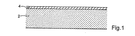
この例は、図1に表わされるように、380℃でSiH4化学物質を使用して、例えば、PECVD(プラズマ化学気相成長法)によって、本明細書において、シリコン酸化物(SiO2)の表面層4が堆積された200mmの典型的な直径および750μmの厚みを有するバルクゲルマニウム(したがって、良好な結晶電気特性を有する)のプレート2を使用する。
An example of this is shown in FIG. 1 using SiH 4 chemistry at 380 ° C., for example by PECVD (Plasma Chemical Vapor Deposition), in this specification of silicon oxide (SiO 2 ). A
表面層がない、または様々な種類の1つまたは複数の表面層を有するゲルマニウムプレート2が、代わりに使用され得る。
A
シリコン酸化物層4は、緻密化(例えば、窒素中で600℃で1時間)によって調製され得る。ゲルマニウムプレート2−シリコン酸化物層4の構造は、次いで、例えば、化学洗浄および/または親水性接合のための化学機械的研磨によって、以下に記載される接合に関して準備される。
The
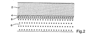
図1において表されたこの構造は、次いで、熱膨張率がゲルマニウムと異なる材料、例えば、シリコン(Si)からなる基板6に接合され、支持体を形成する。シリコン(Si)からなる基板6上には、層、例えば、熱酸化によって形成されたシリコン酸化物(SiO2)の層8が形成され、以降の接合を促進する(酸化物/酸化物接合は、よく実証された技術である)。
This structure represented in FIG. 1 is then bonded to a
シリコン基板6(ここで、介在するシリコン酸化物層4、8とともに適用可能)上のゲルマニウムプレート2のアセンブリは、図2において接合する間を表される。
The assembly of the
この接合は、例えば、200℃で2時間のオーブンで強固にされ得る。 This bonding can be strengthened, for example, in an oven at 200 ° C. for 2 hours.
この接合は、有利には、例えば、100℃〜200℃の高温で実行されることができ、以降の熱処理および特に破断熱処理によって生成される応力の一部を補償することができる応力を、構造内生成し、それによって、破損の危険を低減する。 This joining can advantageously be carried out at a high temperature, for example between 100 ° C. and 200 ° C., and stresses that can compensate for part of the stress produced by the subsequent heat treatment and in particular the fracture heat treatment, In-house, thereby reducing the risk of breakage.
ゲルマニウムプレート2は、次いで、研削、その後の化学機械的研磨、および適切な場合には化学エッチング(研磨は、良好な最終粗さを生成し、化学エッチングは、研削によって生成された欠陥を取り除く)の組み合わせによって薄くされることが好ましい。構造の完全性を保証すれば(特に、構造のあまりにも高い温度上昇を必要としなければ)、他の薄化技術が使用されることができる。
The
ゲルマニウムの最終厚みは、ゲルマニウム/シリコンアセンブリの機械的挙動が、本質的にシリコン6によって影響されるようになっていなければならず、その結果、温度に応じたアセンブリの機械的挙動は、ホモ構造の機械的挙動に類似し、以降の熱処理の間、および特に破断熱処理の間(さらに特に構造の破断の瞬間に)に、構造内に蓄積された弾性エネルギーが、構造破損をもたらさないようにより正確になる。1μm〜50μm、例えば、20μmの厚みは、このゲルマニウム層のために典型的に選択される。
The final thickness of germanium must be such that the mechanical behavior of the germanium / silicon assembly is essentially affected by
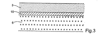
図3に表わされた構造が、次いで得られ、この構造は、したがって本質的に、支持体を形成する基板6(ここでは、200mmの直径の基板のための750μmの典型的な厚みを有するシリコン)、シリコン酸化物の中間層10(上記で言及された2つのシリコン酸化物層4、8のアセンブリに相当する)、厚みが低減された、例えば数ミクロンから数十ミクロンの厚み、例えば20μmの厚みの薄くされたゲルマニウム層3からなる。
The structure represented in FIG. 3 is then obtained, which structure essentially has a
それを生成するために使用される工程のために、薄くされたゲルマニウム層3の粗さおよび結晶構造は、バルクゲルマニウム基板に近く、したがって、ゲルマニウムの薄くされた層3から、以下に記載されるように形成された薄層の結晶および電気的特性は、特に良好である。
Due to the process used to produce it, the roughness and crystal structure of the thinned
以下に説明されるように、薄くされたゲルマニウム層3の低減された厚み、および支持体を形成するシリコン基板6へのその接合は、それにもかかわらず、バルクゲルマニウム基板とは異なる機械的挙動を有する構造を生成し、以下に記載される分離ステップで使用される場合、有利となるであろう。
As will be explained below, the reduced thickness of the thinned
さらに、ゲルマニウムよりシリコンの熱伝導率が高いために、この(ゲルマニウム/シリコン)構造は、ゲルマニウム基板を使用する解決法より以降の技術ステップの間に、より良好な熱の排出を示す。 Furthermore, because of the higher thermal conductivity of silicon than germanium, this (germanium / silicon) structure exhibits better heat dissipation during subsequent technical steps than the solution using a germanium substrate.
したがって、記載された図3において表された構造は、次に記載されるように、薄層、ここでは、ゲルマニウムの転写を可能にする特に有利なドナー構造を構成する。 Thus, the structure depicted in FIG. 3 described constitutes a particularly advantageous donor structure that allows the transfer of a thin layer, here germanium, as described next.
薄層(本質的に、本明細書で記載された例におけるシリコン基板)を受ける支持体に接合する前に、予め生成されかつ、図3に表わされた構造は、次のステップを行うことにより準備されることができる。すなわち、
従来どおり、例えば、PECVDによって二酸化ケイ素(SiO2)の層を堆積するステップと、
400℃〜600℃で1時間、窒素中でシリコン酸化物層を任意に緻密化するステップと、
洗浄および/または化学機械研磨ステップ(親水性接合との適合性を向上するために)とである。
Prior to bonding to a support that receives a thin layer (essentially the silicon substrate in the example described herein), the structure previously produced and represented in FIG. Can be prepared by. That is,
Conventionally, for example, depositing a layer of silicon dioxide (SiO 2 ) by PECVD;
Optionally densifying the silicon oxide layer in nitrogen at 400 ° C. to 600 ° C. for 1 hour;
Cleaning and / or chemical mechanical polishing steps (to improve compatibility with hydrophilic bonding).
あるいは、もちろん、いかなる酸化物でも必ずしも堆積することはできず、薄層を受ける支持体にそれを直接接合するために、ゲルマニウム表面を調製する。 Alternatively, of course, any oxide cannot necessarily be deposited, and a germanium surface is prepared to bond it directly to a support that receives a thin layer.
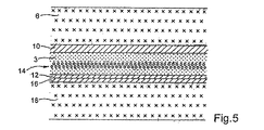
弱められた領域14は、転写される薄膜の厚みに相当する深さ(一般に、約数百ナノメータ程度、例えば、数十ナノメータ〜1000nm)で、例えば、ガス種、ここでは、水素イオン(H+)を数keV〜250keVのエネルギーで、3×10¹⁶〜7×10¹⁶H+/cm2のドーズレートで、典型的には、100keVの注入エネルギーおよび5×1016H+/cm2のドーズレートでの注入によって、薄くされたゲルマニウム層3内に生成され、約700nmの注入深さが得られる。
The weakened
注入ステップは、シリコン酸化物層(SiO2)層の形成後、および、例えば、表面を洗浄する前に行なわれる。 The implantation step is performed after the formation of the silicon oxide layer (SiO 2 ) layer and before, for example, cleaning the surface.
この注入ステップ後に、および適用可能なこれらの準備ステップの場合に、ドナー構造は、したがって、図4に示される。 After this implantation step and in the case of these preparation steps where applicable, the donor structure is thus shown in FIG.
その構造は、次いで、(薄くされたゲルマニウム層3、つまり、注入を受けた表面に堆積されたシリコン酸化物層12によって)、例えば、薄層が転写される支持体に対する親水性接合によって接合され、ここで、支持体は、主として、シリコン基板18(一般には、200mmの厚みの基板に関して厚み約750μmの)からなり、シリコン酸化物(SiO2)層16によって被覆される。
The structure is then joined (by a thinned
したがって、図5に表わされたアセンブリが得られ、そのアセンブリは、弱められた領域14に破断を形成するために、一般的には、200℃〜500℃(ここでは、例えば、330℃で)で熱処理ステップを受ける。 Thus, the assembly depicted in FIG. 5 is obtained, which is typically 200 ° C. to 500 ° C. (here, for example, at 330 ° C.) to form a break in the weakened region 14. ) Undergo a heat treatment step.
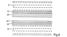
これは、シリコン酸化物層16によって被覆されたシリコン基板18によって形成された支持体を分離し、シリコン基板は、これ以降、ゲルマニウム(薄くされた層3からもたらされる)の薄層22を支持し、図6に表わされるように、この転写された薄層からドナー構造が剥離される。
This separates the support formed by the
薄くされたゲルマニウム層3は、シリコン基板6、18(少なくとも約1〜10程度の比率で図中に実際に図示される)比較して薄いため、また2つの基板6、18(ここでは、同じ材料から作られる)の機械的適合性(ここでは、熱膨張の観点から)のため、上記に言及される(および図5に表わされる)アセンブリは、ホモ構造として本質的に作用し、したがって、多大な破損の危険なしに、破断熱処理ステップの間に良好な機械的挙動を示す。
The thinned
破断の瞬間に構造内に蓄積された弾性エネルギーの解放は制御され、破断後に得られる構造の破損をもたらさない。 The release of the elastic energy stored in the structure at the moment of rupture is controlled and does not cause damage to the structure obtained after rupture.
この薄膜22が、薄くされたゲルマニウム層3に由来し、その電気的特性は、既に述べられたように、初期のゲルマニウムプレートの電気的特性に近いので、弱められた領域の破断(したがって、図5のアセンブリの分離)ステップ後、したがって、シリコン酸化物層24で被覆されたシリコン基板18は、良好な電気的特性を有するゲルマニウムの薄膜22を支持する。
This
したがって、研磨や熱アニールタイプの仕上げ処理を終了した後に適用可能な場合に、特に有益なゲルマニウム層の電気的特性を有するGeOI(つまり、絶縁体上のゲルマニウムの)のプレートが得られる。 Thus, a GeOI (ie germanium-on-insulator) plate with particularly advantageous germanium layer electrical properties is obtained when applicable after finishing a polishing or thermal annealing type finish.
主としてシリコン基板6および残存するゲルマニウム層20(薄層22から剥離された薄くされたゲルマニウム層3)からなるドナー構造は、次いで、この場合に残存層20から得られたゲルマニウムの新しい薄層の転写のために、ドナー構造として再び使用されるために、(例えば、研削および/または研磨技術によって)再利用され得る(これは、薄層22から剥離された場合でさえ、ドナー構造は、図3において予め表されるように本質的に構成されるからである)。
The donor structure consisting mainly of the
1つの有利な実行可能性によれば、薄くされた層3またはドナー構造のゲルマニウムの残存層20は、その構造上にゲルマニウムのエピタキシャル成長のための種として役立つことができる。薄くされた(または残存)層の結晶品質のために、このエピタキシャル層の結晶品質は、バルクゲルマニウム基板の結晶品質に近いであろう。したがって、薄層転写工程は、エピタキシャル層を使用して繰り返され得る。
According to one advantageous feasibility, the thinned
あるいは、(薄くされた層3または残存層20上に)エピタキシャルで連続的に反復してゲルマニウム(数ミクロン、例えば2μmの厚みに)およびシリコン(典型的には、数ナノメータの厚みに)が生成されて、これら2つの材料の交互スタック、Si/Ge/Si/Geなどを生成することができる。
Alternatively, epitaxially (continuously on the thinned
エピタキシャルシリコン層は、非常に薄いので、ゲルマニウムは、良好な結晶品質が、エピタキシャルゲルマニウム層内で維持されるように、その格子定数を付与する。 Since the epitaxial silicon layer is very thin, germanium imparts its lattice constant so that good crystal quality is maintained within the epitaxial germanium layer.
他方、エピタキシャル層および初期のゲルマニウム層3、20の組み合わされた厚みは、シリコン基板によって付与されるように得られる構造の温度に応じて、機械的挙動には十分に小さいままでなければならない。
On the other hand, the combined thickness of the epitaxial layer and the
この変形例は、連続転写中に停止層として薄いシリコン層を使用することができる。 This variation can use a thin silicon layer as a stop layer during continuous transfer.
下記の工程も使用され得る。すなわち、
注入は、その層において、転写される薄膜を画定するために、スタック(外部層)の頂部に配置されたゲルマニウムのエピタキシャル層で達成され、
上記されるように、薄膜は、転写され、
外部ゲルマニウム層の残りは、選択エッチング(例えば、H2O2エッチング)によって取り除かれ、
シリコン停止層は、次いで、選択エッチング(例えば、TMAH(テトラメチルアンモニウム水酸化物)を使用すること)によって取り除かれ、
工程は、次のゲルマニウム層で繰り返される。
The following steps can also be used. That is,
Implantation is accomplished with an epitaxial layer of germanium placed on top of the stack (outer layer) to define a thin film to be transferred in that layer;
As noted above, the thin film is transferred and
The remainder of the outer germanium layer is removed by selective etching (eg, H 2 O 2 etching)
The silicon stop layer is then removed by selective etching (eg, using TMAH (tetramethylammonium hydroxide))
The process is repeated with the next germanium layer.
本方法は、破断後の研磨の使用、したがって、通常生じる不均質な厚みを回避する。 The method avoids the use of post-breaking polishing and thus the non-uniform thickness that normally occurs.
記載された例は、本発明の可能な実施形態のみを構成し、本発明は、それら実施形態に限定されない。 The described examples constitute only possible embodiments of the invention, and the invention is not limited to these embodiments.
Claims (10)
ゲルマニウムのバルク基板からもたらされるゲルマニウムの層(3)またはゲルマニウムのバルク基板を種として使用してエピタキシャル成長させたゲルマニウムの層(3)を含む構造を提供するステップを含み、層(3)が、シリコンから形成される第2の支持体(6、10)に取り付けられ、前記ゲルマニウムの層の最終厚みが、1μm〜50μmであり、前記薄膜転写方法がさらに、
少なくとも1つのガス種を注入することにより、薄層(22)が転写される構造に境界を定める所定の深さで、層(3)内に埋設され弱められた領域(14)を形成するステップと、
第2の支持体(6、10)に取り付けられた層(3)を、シリコンから形成された第1の支持体(18、24)に接合するステップと、
弱められた領域(14)において層(3)を破断するために熱処理を行うステップとを含むことを特徴とする、方法。 A thin film transfer method for transferring a thin layer of germanium (22) onto a first support (18, 24) formed from silicon,
Comprising the steps of: providing a structure comprising a layer (3) or a layer of gate Rumaniumu epitaxially grown using germanium bulk substrate as a seed (3) of germanium resulting from germanium bulk substrate, a layer (3), Attached to a second support (6, 10) formed of silicon, the final thickness of the germanium layer is 1 μm to 50 μm, and the thin film transfer method further comprises:
Forming a weakened region (14) embedded in layer (3) at a predetermined depth that delimits the structure to which thin layer (22) is transferred by injecting at least one gas species When,
Bonding the layer (3) attached to the second support (6, 10) to the first support (18, 24) formed from silicon;
Performing a heat treatment to break the layer (3) in the weakened region (14).
エピタキシャル層を第3の支持体に接合するステップと、
弱められた領域においてエピタキシャル層を破断するステップとを含む、請求項7に記載の薄層転写方法。 Forming a buried and weakened region in the epitaxial layer;
Bonding the epitaxial layer to a third support;
8. A thin layer transfer method according to claim 7, comprising the step of breaking the epitaxial layer in the weakened region.
Applications Claiming Priority (3)
| Application Number | Priority Date | Filing Date | Title |
|---|---|---|---|
| FR0508555A FR2889887B1 (en) | 2005-08-16 | 2005-08-16 | METHOD FOR DEFERING A THIN LAYER ON A SUPPORT |
| FR0508555 | 2005-08-16 | ||
| PCT/FR2006/001945 WO2007020351A1 (en) | 2005-08-16 | 2006-08-11 | Method of transferring a thin film onto a support |
Publications (3)
| Publication Number | Publication Date |
|---|---|
| JP2009504392A JP2009504392A (en) | 2009-02-05 |
| JP2009504392A5 JP2009504392A5 (en) | 2010-10-21 |
| JP5258564B2 true JP5258564B2 (en) | 2013-08-07 |
Family
ID=36591309
Family Applications (1)
| Application Number | Title | Priority Date | Filing Date |
|---|---|---|---|
| JP2008526524A Expired - Fee Related JP5258564B2 (en) | 2005-08-16 | 2006-08-11 | Method for transferring a thin film onto a support |
Country Status (5)
| Country | Link |
|---|---|
| US (1) | US8142593B2 (en) |
| EP (1) | EP1922752B1 (en) |
| JP (1) | JP5258564B2 (en) |
| FR (1) | FR2889887B1 (en) |
| WO (1) | WO2007020351A1 (en) |
Families Citing this family (21)
| Publication number | Priority date | Publication date | Assignee | Title |
|---|---|---|---|---|
| FR2748851B1 (en) | 1996-05-15 | 1998-08-07 | Commissariat Energie Atomique | PROCESS FOR PRODUCING A THIN FILM OF SEMICONDUCTOR MATERIAL |
| FR2773261B1 (en) | 1997-12-30 | 2000-01-28 | Commissariat Energie Atomique | METHOD FOR THE TRANSFER OF A THIN FILM COMPRISING A STEP OF CREATING INCLUSIONS |
| FR2848336B1 (en) * | 2002-12-09 | 2005-10-28 | Commissariat Energie Atomique | METHOD FOR PRODUCING A STRESS STRUCTURE FOR DISSOCIATING |
| FR2856844B1 (en) * | 2003-06-24 | 2006-02-17 | Commissariat Energie Atomique | HIGH PERFORMANCE CHIP INTEGRATED CIRCUIT |
| FR2861497B1 (en) * | 2003-10-28 | 2006-02-10 | Soitec Silicon On Insulator | METHOD FOR CATASTROPHIC TRANSFER OF A FINE LAYER AFTER CO-IMPLANTATION |
| FR2891281B1 (en) | 2005-09-28 | 2007-12-28 | Commissariat Energie Atomique | METHOD FOR MANUFACTURING A THIN FILM ELEMENT |
| FR2910179B1 (en) | 2006-12-19 | 2009-03-13 | Commissariat Energie Atomique | METHOD FOR MANUFACTURING THIN LAYERS OF GaN BY IMPLANTATION AND RECYCLING OF A STARTING SUBSTRATE |
| JP4290745B2 (en) * | 2007-03-16 | 2009-07-08 | 豊田合成株式会社 | Method for manufacturing group III-V semiconductor device |
| FR2947098A1 (en) | 2009-06-18 | 2010-12-24 | Commissariat Energie Atomique | METHOD OF TRANSFERRING A THIN LAYER TO A TARGET SUBSTRATE HAVING A THERMAL EXPANSION COEFFICIENT DIFFERENT FROM THAT OF THE THIN LAYER |
| DE102009053262A1 (en) * | 2009-11-13 | 2011-05-19 | Institut Für Solarenergieforschung Gmbh | A method for forming thin semiconductor layer substrates and method for producing a semiconductor device, in particular a solar cell, with such a semiconductor layer substrate |
| US8367519B2 (en) * | 2009-12-30 | 2013-02-05 | Memc Electronic Materials, Inc. | Method for the preparation of a multi-layered crystalline structure |
| US9257339B2 (en) * | 2012-05-04 | 2016-02-09 | Silicon Genesis Corporation | Techniques for forming optoelectronic devices |
| US8735219B2 (en) | 2012-08-30 | 2014-05-27 | Ziptronix, Inc. | Heterogeneous annealing method and device |
| EP2912685B1 (en) * | 2012-10-26 | 2020-04-08 | RFHIC Corporation | Semiconductor devices with improved reliability and operating life and methods of manufacturing the same |
| US9356188B2 (en) | 2013-09-06 | 2016-05-31 | Veeco Instruments, Inc. | Tensile separation of a semiconducting stack |
| KR102180089B1 (en) | 2013-12-30 | 2020-11-18 | 삼성디스플레이 주식회사 | Method of manufacturing flexible substrate and method of manufacturing display device using the same |
| KR101889352B1 (en) | 2016-09-13 | 2018-08-20 | 한국과학기술연구원 | Semicondutor device including strained germanium and method for manufacturing the same |
| FR3074608B1 (en) * | 2017-12-05 | 2019-12-06 | Soitec | PROCESS FOR THE PREPARATION OF A RESIDUE OF A DONOR SUBSTRATE, SUBSTRATE OBTAINED AT THE END OF THIS PROCESS, AND USE OF SUCH A SUBSTRATE |
| FR3079346B1 (en) * | 2018-03-26 | 2020-05-29 | Soitec | METHOD FOR MANUFACTURING A DONOR SUBSTRATE FOR TRANSFERRING A PIEZOELECTRIC LAYER, AND METHOD FOR TRANSFERRING SUCH A PIEZOELECTRIC LAYER |
| US11664357B2 (en) | 2018-07-03 | 2023-05-30 | Adeia Semiconductor Bonding Technologies Inc. | Techniques for joining dissimilar materials in microelectronics |
| WO2020061234A1 (en) * | 2018-09-19 | 2020-03-26 | Akash Systems, Inc. | Systems and methods for satellite communication |
Family Cites Families (250)
| Publication number | Priority date | Publication date | Assignee | Title |
|---|---|---|---|---|
| US3915757A (en) | 1972-08-09 | 1975-10-28 | Niels N Engel | Ion plating method and product therefrom |
| US3913520A (en) | 1972-08-14 | 1975-10-21 | Precision Thin Film Corp | High vacuum deposition apparatus |
| US3993909A (en) | 1973-03-16 | 1976-11-23 | U.S. Philips Corporation | Substrate holder for etching thin films |
| FR2245779B1 (en) | 1973-09-28 | 1978-02-10 | Cit Alcatel | |
| US3901423A (en) | 1973-11-26 | 1975-08-26 | Purdue Research Foundation | Method for fracturing crystalline materials |
| US4170662A (en) | 1974-11-05 | 1979-10-09 | Eastman Kodak Company | Plasma plating |
| US4121334A (en) | 1974-12-17 | 1978-10-24 | P. R. Mallory & Co. Inc. | Application of field-assisted bonding to the mass production of silicon type pressure transducers |
| US3957107A (en) | 1975-02-27 | 1976-05-18 | The United States Of America As Represented By The Secretary Of The Air Force | Thermal switch |
| US4039416A (en) | 1975-04-21 | 1977-08-02 | White Gerald W | Gasless ion plating |
| GB1542299A (en) | 1976-03-23 | 1979-03-14 | Warner Lambert Co | Blade shields |
| US4028149A (en) | 1976-06-30 | 1977-06-07 | Ibm Corporation | Process for forming monocrystalline silicon carbide on silicon substrates |
| US4074139A (en) | 1976-12-27 | 1978-02-14 | Rca Corporation | Apparatus and method for maskless ion implantation |
| US4108751A (en) | 1977-06-06 | 1978-08-22 | King William J | Ion beam implantation-sputtering |
| US4179324A (en) | 1977-11-28 | 1979-12-18 | Spire Corporation | Process for fabricating thin film and glass sheet laminate |
| DE2849184A1 (en) | 1978-11-13 | 1980-05-22 | Bbc Brown Boveri & Cie | METHOD FOR PRODUCING A DISC-SHAPED SILICON SEMICONDUCTOR COMPONENT WITH NEGATIVE BEVELING |
| JPS55104057A (en) | 1979-02-02 | 1980-08-09 | Hitachi Ltd | Ion implantation device |
| US4324631A (en) | 1979-07-23 | 1982-04-13 | Spin Physics, Inc. | Magnetron sputtering of magnetic materials |
| CH640886A5 (en) | 1979-08-02 | 1984-01-31 | Balzers Hochvakuum | METHOD FOR APPLYING HARD WEAR-RESISTANT COATS ON DOCKS. |
| US4244348A (en) | 1979-09-10 | 1981-01-13 | Atlantic Richfield Company | Process for cleaving crystalline materials |
| FR2506344B2 (en) | 1980-02-01 | 1986-07-11 | Commissariat Energie Atomique | SEMICONDUCTOR DOPING PROCESS |
| FR2475068B1 (en) | 1980-02-01 | 1986-05-16 | Commissariat Energie Atomique | SEMICONDUCTOR DOPING PROCESS |
| US4471003A (en) | 1980-11-25 | 1984-09-11 | Cann Gordon L | Magnetoplasmadynamic apparatus and process for the separation and deposition of materials |
| FR2501727A1 (en) | 1981-03-13 | 1982-09-17 | Vide Traitement | PROCESS FOR THE THERMOCHEMICAL TREATMENT OF METALS BY ION BOMBING |
| US4361600A (en) | 1981-11-12 | 1982-11-30 | General Electric Company | Method of making integrated circuits |
| US4412868A (en) | 1981-12-23 | 1983-11-01 | General Electric Company | Method of making integrated circuits utilizing ion implantation and selective epitaxial growth |
| US4486247A (en) | 1982-06-21 | 1984-12-04 | Westinghouse Electric Corp. | Wear resistant steel articles with carbon, oxygen and nitrogen implanted in the surface thereof |
| FR2529383A1 (en) | 1982-06-24 | 1983-12-30 | Commissariat Energie Atomique | MECHANICAL SCANNING TARGET HOLDER USABLE IN PARTICULAR FOR THE IMPLANTATION OF IORIS |
| FR2537768A1 (en) | 1982-12-08 | 1984-06-15 | Commissariat Energie Atomique | METHOD AND DEVICE FOR OBTAINING SPATIALLY MODULATED DENSITY PARTICLE BEAMS, APPLICATION TO ION ETCHING AND IMPLANTATION |
| FR2537777A1 (en) | 1982-12-10 | 1984-06-15 | Commissariat Energie Atomique | METHOD AND DEVICE FOR IMPLANTATION OF PARTICLES IN A SOLID |
| DE3246480A1 (en) | 1982-12-15 | 1984-06-20 | Wacker-Chemitronic Gesellschaft für Elektronik-Grundstoffe mbH, 8263 Burghausen | METHOD FOR THE PRODUCTION OF SEMICONDUCTOR DISC WITH CUTTING DISC REAR SIDE |
| US4500563A (en) | 1982-12-15 | 1985-02-19 | Pacific Western Systems, Inc. | Independently variably controlled pulsed R.F. plasma chemical vapor processing |
| US4468309A (en) | 1983-04-22 | 1984-08-28 | White Engineering Corporation | Method for resisting galling |
| GB2144343A (en) | 1983-08-02 | 1985-03-06 | Standard Telephones Cables Ltd | Optical fibre manufacture |
| US4567505A (en) | 1983-10-27 | 1986-01-28 | The Board Of Trustees Of The Leland Stanford Junior University | Heat sink and method of attaching heat sink to a semiconductor integrated circuit and the like |
| JPS6088535U (en) | 1983-11-24 | 1985-06-18 | 住友電気工業株式会社 | semiconductor wafer |
| FR2558263B1 (en) | 1984-01-12 | 1986-04-25 | Commissariat Energie Atomique | DIRECTIVE ACCELEROMETER AND METHOD FOR MANUFACTURING IT WITH MICROLITHOGRAPHY |
| GB2155024A (en) | 1984-03-03 | 1985-09-18 | Standard Telephones Cables Ltd | Surface treatment of plastics materials |
| FR2563377B1 (en) | 1984-04-19 | 1987-01-23 | Commissariat Energie Atomique | METHOD FOR MANUFACTURING AN INSULATING LAYER BURIED IN A SEMICONDUCTOR SUBSTRATE, BY ION IMPLANTATION |
| US4542863A (en) | 1984-07-23 | 1985-09-24 | Larson Edwin L | Pipe-thread sealing tape reel with tape retarding element |
| US4566403A (en) | 1985-01-30 | 1986-01-28 | Sovonics Solar Systems | Apparatus for microwave glow discharge deposition |
| US4837172A (en) | 1986-07-18 | 1989-06-06 | Matsushita Electric Industrial Co., Ltd. | Method for removing impurities existing in semiconductor substrate |
| US4717683A (en) | 1986-09-23 | 1988-01-05 | Motorola Inc. | CMOS process |
| US4764394A (en) | 1987-01-20 | 1988-08-16 | Wisconsin Alumni Research Foundation | Method and apparatus for plasma source ion implantation |
| JPS63254762A (en) | 1987-04-13 | 1988-10-21 | Nissan Motor Co Ltd | Cmos semiconductor device |
| US4847792A (en) | 1987-05-04 | 1989-07-11 | Texas Instruments Incorporated | Process and apparatus for detecting aberrations in production process operations |
| SE458398B (en) | 1987-05-27 | 1989-03-20 | H Biverot | LIGHT DETECTING AND LIGHTING DETERMINATION DEVICE |
| FR2616590B1 (en) | 1987-06-15 | 1990-03-02 | Commissariat Energie Atomique | METHOD FOR MANUFACTURING AN INSULATOR LAYER BURIED IN A SEMICONDUCTOR SUBSTRATE BY ION IMPLANTATION AND SEMICONDUCTOR STRUCTURE COMPRISING THIS LAYER |
| US4956698A (en) | 1987-07-29 | 1990-09-11 | The United States Of America As Represented By The Department Of Commerce | Group III-V compound semiconductor device having p-region formed by Be and Group V ions |
| US4846928A (en) | 1987-08-04 | 1989-07-11 | Texas Instruments, Incorporated | Process and apparatus for detecting aberrations in production process operations |
| US4887005A (en) | 1987-09-15 | 1989-12-12 | Rough J Kirkwood H | Multiple electrode plasma reactor power distribution system |
| US5015353A (en) | 1987-09-30 | 1991-05-14 | The United States Of America As Represented By The Secretary Of The Navy | Method for producing substoichiometric silicon nitride of preselected proportions |
| US5138422A (en) | 1987-10-27 | 1992-08-11 | Nippondenso Co., Ltd. | Semiconductor device which includes multiple isolated semiconductor segments on one chip |
| GB8725497D0 (en) | 1987-10-30 | 1987-12-02 | Atomic Energy Authority Uk | Isolation of silicon |
| US5200805A (en) | 1987-12-28 | 1993-04-06 | Hughes Aircraft Company | Silicon carbide:metal carbide alloy semiconductor and method of making the same |
| US4904610A (en) | 1988-01-27 | 1990-02-27 | General Instrument Corporation | Wafer level process for fabricating passivated semiconductor devices |
| DE3803424C2 (en) | 1988-02-05 | 1995-05-18 | Gsf Forschungszentrum Umwelt | Method for the quantitative, depth-differential analysis of solid samples |
| JP2666945B2 (en) | 1988-02-08 | 1997-10-22 | 株式会社東芝 | Method for manufacturing semiconductor device |
| US4894709A (en) | 1988-03-09 | 1990-01-16 | Massachusetts Institute Of Technology | Forced-convection, liquid-cooled, microchannel heat sinks |
| US4853250A (en) | 1988-05-11 | 1989-08-01 | Universite De Sherbrooke | Process of depositing particulate material on a substrate |
| NL8802028A (en) | 1988-08-16 | 1990-03-16 | Philips Nv | METHOD FOR MANUFACTURING AN APPARATUS |
| JP2670623B2 (en) | 1988-09-19 | 1997-10-29 | アネルバ株式会社 | Microwave plasma processing equipment |
| US4952273A (en) | 1988-09-21 | 1990-08-28 | Microscience, Inc. | Plasma generation in electron cyclotron resonance |
| US4996077A (en) | 1988-10-07 | 1991-02-26 | Texas Instruments Incorporated | Distributed ECR remote plasma processing and apparatus |
| US4891329A (en) | 1988-11-29 | 1990-01-02 | University Of North Carolina | Method of forming a nonsilicon semiconductor on insulator structure |
| NL8900388A (en) | 1989-02-17 | 1990-09-17 | Philips Nv | METHOD FOR JOINING TWO OBJECTS |
| JPH02302044A (en) | 1989-05-16 | 1990-12-14 | Fujitsu Ltd | Manufacture of semiconductor device |
| US4929566A (en) | 1989-07-06 | 1990-05-29 | Harris Corporation | Method of making dielectrically isolated integrated circuits using oxygen implantation and expitaxial growth |
| JPH0355822A (en) | 1989-07-25 | 1991-03-11 | Shin Etsu Handotai Co Ltd | Manufacture of substrate for forming semiconductor element |
| US4948458A (en) | 1989-08-14 | 1990-08-14 | Lam Research Corporation | Method and apparatus for producing magnetically-coupled planar plasma |
| US5036023A (en) | 1989-08-16 | 1991-07-30 | At&T Bell Laboratories | Rapid thermal processing method of making a semiconductor device |
| US5013681A (en) | 1989-09-29 | 1991-05-07 | The United States Of America As Represented By The Secretary Of The Navy | Method of producing a thin silicon-on-insulator layer |
| US5310446A (en) | 1990-01-10 | 1994-05-10 | Ricoh Company, Ltd. | Method for producing semiconductor film |
| JPH0650738B2 (en) | 1990-01-11 | 1994-06-29 | 株式会社東芝 | Semiconductor device and manufacturing method thereof |
| US5034343A (en) | 1990-03-08 | 1991-07-23 | Harris Corporation | Manufacturing ultra-thin wafer using a handle wafer |
| CN1018844B (en) | 1990-06-02 | 1992-10-28 | 中国科学院兰州化学物理研究所 | Antirust dry film lubricant |
| JPH0719739B2 (en) | 1990-09-10 | 1995-03-06 | 信越半導体株式会社 | Bonded wafer manufacturing method |
| US5198371A (en) | 1990-09-24 | 1993-03-30 | Biota Corp. | Method of making silicon material with enhanced surface mobility by hydrogen ion implantation |
| US5618739A (en) | 1990-11-15 | 1997-04-08 | Seiko Instruments Inc. | Method of making light valve device using semiconductive composite substrate |
| US5300788A (en) | 1991-01-18 | 1994-04-05 | Kopin Corporation | Light emitting diode bars and arrays and method of making same |
| DE4106288C2 (en) | 1991-02-28 | 2001-05-31 | Bosch Gmbh Robert | Sensor for measuring pressures or accelerations |
| JP2812405B2 (en) | 1991-03-15 | 1998-10-22 | 信越半導体株式会社 | Semiconductor substrate manufacturing method |
| US5110748A (en) | 1991-03-28 | 1992-05-05 | Honeywell Inc. | Method for fabricating high mobility thin film transistors as integrated drivers for active matrix display |
| US5442205A (en) | 1991-04-24 | 1995-08-15 | At&T Corp. | Semiconductor heterostructure devices with strained semiconductor layers |
| US5256581A (en) | 1991-08-28 | 1993-10-26 | Motorola, Inc. | Silicon film with improved thickness control |
| FR2681472B1 (en) | 1991-09-18 | 1993-10-29 | Commissariat Energie Atomique | PROCESS FOR PRODUCING THIN FILMS OF SEMICONDUCTOR MATERIAL. |
| JP3416163B2 (en) | 1992-01-31 | 2003-06-16 | キヤノン株式会社 | Semiconductor substrate and manufacturing method thereof |
| JPH05235312A (en) | 1992-02-19 | 1993-09-10 | Fujitsu Ltd | Semiconductor substrate and its manufacture |
| US5614019A (en) | 1992-06-08 | 1997-03-25 | Air Products And Chemicals, Inc. | Method for the growth of industrial crystals |
| US5234535A (en) | 1992-12-10 | 1993-08-10 | International Business Machines Corporation | Method of producing a thin silicon-on-insulator layer |
| WO1994017558A1 (en) | 1993-01-29 | 1994-08-04 | The Regents Of The University Of California | Monolithic passive component |
| US5400458A (en) | 1993-03-31 | 1995-03-28 | Minnesota Mining And Manufacturing Company | Brush segment for industrial brushes |
| FR2714524B1 (en) | 1993-12-23 | 1996-01-26 | Commissariat Energie Atomique | PROCESS FOR MAKING A RELIEF STRUCTURE ON A SUPPORT IN SEMICONDUCTOR MATERIAL |
| DE69432323T2 (en) | 1993-12-28 | 2003-12-11 | Honda Giken Kogyo K.K., Tokio/Tokyo | Gas supply mechanism and device for determining and displaying the amount of gas for a gas engine |
| DE4400985C1 (en) | 1994-01-14 | 1995-05-11 | Siemens Ag | Method for producing a three-dimensional circuit arrangement |
| FR2715503B1 (en) | 1994-01-26 | 1996-04-05 | Commissariat Energie Atomique | Substrate for integrated components comprising a thin layer and its production method. |
| FR2715501B1 (en) | 1994-01-26 | 1996-04-05 | Commissariat Energie Atomique | Method for depositing semiconductor wafers on a support. |
| FR2715502B1 (en) | 1994-01-26 | 1996-04-05 | Commissariat Energie Atomique | Structure having cavities and method for producing such a structure. |
| JP3293736B2 (en) | 1996-02-28 | 2002-06-17 | キヤノン株式会社 | Semiconductor substrate manufacturing method and bonded substrate |
| US5880010A (en) | 1994-07-12 | 1999-03-09 | Sun Microsystems, Inc. | Ultrathin electronics |
| JPH0851103A (en) | 1994-08-08 | 1996-02-20 | Fuji Electric Co Ltd | Thin film generation method |
| US5524339A (en) | 1994-09-19 | 1996-06-11 | Martin Marietta Corporation | Method for protecting gallium arsenide mmic air bridge structures |
| FR2725074B1 (en) | 1994-09-22 | 1996-12-20 | Commissariat Energie Atomique | METHOD FOR MANUFACTURING A STRUCTURE COMPRISING A THIN SEMI-CONDUCTIVE LAYER ON A SUBSTRATE |
| US5567654A (en) | 1994-09-28 | 1996-10-22 | International Business Machines Corporation | Method and workpiece for connecting a thin layer to a monolithic electronic module's surface and associated module packaging |
| JP3743519B2 (en) | 1994-10-18 | 2006-02-08 | コーニンクレッカ フィリップス エレクトロニクス エヌ ヴィ | Method for producing silicon-oxide thin layer |
| EP0799495A4 (en) | 1994-11-10 | 1999-11-03 | Lawrence Semiconductor Researc | SILICON-GERMANIUM-CARBON COMPOSITIONS AND RELATED PROCESSES |
| EP0717437B1 (en) | 1994-12-12 | 2002-04-24 | Advanced Micro Devices, Inc. | Method of forming buried oxide layers |
| JP3381443B2 (en) | 1995-02-02 | 2003-02-24 | ソニー株式会社 | Method for separating semiconductor layer from substrate, method for manufacturing semiconductor device, and method for manufacturing SOI substrate |
| FR2736934B1 (en) | 1995-07-21 | 1997-08-22 | Commissariat Energie Atomique | METHOD FOR MANUFACTURING A STRUCTURE WITH A USEFUL LAYER MAINTAINED A DISTANCE FROM A SUBSTRATE BY STOPS, AND FOR DISCONNECTING SUCH A LAYER |
| FR2738671B1 (en) | 1995-09-13 | 1997-10-10 | Commissariat Energie Atomique | PROCESS FOR PRODUCING THIN FILMS WITH SEMICONDUCTOR MATERIAL |
| CN1132223C (en) | 1995-10-06 | 2003-12-24 | 佳能株式会社 | Semiconductor substrate and producing method thereof |
| FR2744285B1 (en) | 1996-01-25 | 1998-03-06 | Commissariat Energie Atomique | METHOD FOR TRANSFERRING A THIN FILM FROM AN INITIAL SUBSTRATE TO A FINAL SUBSTRATE |
| FR2747506B1 (en) | 1996-04-11 | 1998-05-15 | Commissariat Energie Atomique | PROCESS FOR OBTAINING A THIN FILM OF SEMICONDUCTOR MATERIAL INCLUDING IN PARTICULAR ELECTRONIC COMPONENTS |
| FR2748851B1 (en) | 1996-05-15 | 1998-08-07 | Commissariat Energie Atomique | PROCESS FOR PRODUCING A THIN FILM OF SEMICONDUCTOR MATERIAL |
| FR2748850B1 (en) | 1996-05-15 | 1998-07-24 | Commissariat Energie Atomique | PROCESS FOR MAKING A THIN FILM OF SOLID MATERIAL AND APPLICATIONS OF THIS PROCESS |
| US5863832A (en) | 1996-06-28 | 1999-01-26 | Intel Corporation | Capping layer in interconnect system and method for bonding the capping layer onto the interconnect system |
| US5897331A (en) | 1996-11-08 | 1999-04-27 | Midwest Research Institute | High efficiency low cost thin film silicon solar cell design and method for making |
| US6127199A (en) | 1996-11-12 | 2000-10-03 | Seiko Epson Corporation | Manufacturing method of active matrix substrate, active matrix substrate and liquid crystal display device |
| SG65697A1 (en) | 1996-11-15 | 1999-06-22 | Canon Kk | Process for producing semiconductor article |
| US6054363A (en) | 1996-11-15 | 2000-04-25 | Canon Kabushiki Kaisha | Method of manufacturing semiconductor article |
| DE19648501A1 (en) | 1996-11-22 | 1998-05-28 | Max Planck Gesellschaft | Method for removable connection and finally separation of reversibly bonded and polished plates |
| KR100232886B1 (en) | 1996-11-23 | 1999-12-01 | 김영환 | SOI wafer manufacturing method |
| DE19648759A1 (en) | 1996-11-25 | 1998-05-28 | Max Planck Gesellschaft | Method of manufacturing microstructures |
| FR2756847B1 (en) | 1996-12-09 | 1999-01-08 | Commissariat Energie Atomique | METHOD FOR SEPARATING AT LEAST TWO ELEMENTS OF A STRUCTURE IN CONTACT WITH THEM BY ION IMPLANTATION |
| EP0849788B1 (en) | 1996-12-18 | 2004-03-10 | Canon Kabushiki Kaisha | Process for producing semiconductor article by making use of a substrate having a porous semiconductor layer |
| FR2758907B1 (en) | 1997-01-27 | 1999-05-07 | Commissariat Energie Atomique | METHOD FOR OBTAINING A THIN FILM, PARTICULARLY A SEMICONDUCTOR, WITH A PROTECTED AREA OF IONS, AND INVOLVING AN ION IMPLANTATION STEP |
| JP3114643B2 (en) | 1997-02-20 | 2000-12-04 | 日本電気株式会社 | Semiconductor substrate structure and manufacturing method |
| JPH10275752A (en) | 1997-03-28 | 1998-10-13 | Ube Ind Ltd | Laminated wafer, method for manufacturing the same, and substrate |
| US6013954A (en) | 1997-03-31 | 2000-01-11 | Nec Corporation | Semiconductor wafer having distortion-free alignment regions |
| US6251754B1 (en) | 1997-05-09 | 2001-06-26 | Denso Corporation | Semiconductor substrate manufacturing method |
| US6159824A (en) | 1997-05-12 | 2000-12-12 | Silicon Genesis Corporation | Silicon-on-silicon wafer bonding process using a thin film blister-separation method |
| US6033974A (en) * | 1997-05-12 | 2000-03-07 | Silicon Genesis Corporation | Method for controlled cleaving process |
| US6150239A (en) | 1997-05-31 | 2000-11-21 | Max Planck Society | Method for the transfer of thin layers monocrystalline material onto a desirable substrate |
| US5877070A (en) | 1997-05-31 | 1999-03-02 | Max-Planck Society | Method for the transfer of thin layers of monocrystalline material to a desirable substrate |
| EP0996967B1 (en) | 1997-06-30 | 2008-11-19 | Max-Planck-Gesellschaft zur Förderung der Wissenschaften e.V. | Method for producing layered structures on a semiconductor substrate, semiconductor substrate and semiconductor components produced according to said method |
| US6054369A (en) | 1997-06-30 | 2000-04-25 | Intersil Corporation | Lifetime control for semiconductor devices |
| US6097096A (en) | 1997-07-11 | 2000-08-01 | Advanced Micro Devices | Metal attachment method and structure for attaching substrates at low temperatures |
| US6534380B1 (en) | 1997-07-18 | 2003-03-18 | Denso Corporation | Semiconductor substrate and method of manufacturing the same |
| US6316820B1 (en) | 1997-07-25 | 2001-11-13 | Hughes Electronics Corporation | Passivation layer and process for semiconductor devices |
| US6103599A (en) | 1997-07-25 | 2000-08-15 | Silicon Genesis Corporation | Planarizing technique for multilayered substrates |
| EP0895282A3 (en) | 1997-07-30 | 2000-01-26 | Canon Kabushiki Kaisha | Method of preparing a SOI substrate by using a bonding process, and SOI substrate produced by the same |
| FR2767416B1 (en) | 1997-08-12 | 1999-10-01 | Commissariat Energie Atomique | PROCESS FOR PRODUCING A THIN FILM OF SOLID MATERIAL |
| FR2767604B1 (en) | 1997-08-19 | 2000-12-01 | Commissariat Energie Atomique | TREATMENT PROCESS FOR MOLECULAR GLUING AND TAKING OFF TWO STRUCTURES |
| US5882987A (en) | 1997-08-26 | 1999-03-16 | International Business Machines Corporation | Smart-cut process for the production of thin semiconductor material films |
| JP3697034B2 (en) | 1997-08-26 | 2005-09-21 | キヤノン株式会社 | Method of manufacturing protrusions having minute openings, and probes or multiprobes using them |
| US5981400A (en) | 1997-09-18 | 1999-11-09 | Cornell Research Foundation, Inc. | Compliant universal substrate for epitaxial growth |
| US5920764A (en) | 1997-09-30 | 1999-07-06 | International Business Machines Corporation | Process for restoring rejected wafers in line for reuse as new |
| JP2998724B2 (en) | 1997-11-10 | 2000-01-11 | 日本電気株式会社 | Manufacturing method of bonded SOI substrate |
| FR2771852B1 (en) | 1997-12-02 | 1999-12-31 | Commissariat Energie Atomique | METHOD FOR THE SELECTIVE TRANSFER OF A MICROSTRUCTURE, FORMED ON AN INITIAL SUBSTRATE, TO A FINAL SUBSTRATE |
| FR2773261B1 (en) | 1997-12-30 | 2000-01-28 | Commissariat Energie Atomique | METHOD FOR THE TRANSFER OF A THIN FILM COMPRISING A STEP OF CREATING INCLUSIONS |
| SG70141A1 (en) | 1997-12-26 | 2000-01-25 | Canon Kk | Sample separating apparatus and method and substrate manufacturing method |
| JP3501642B2 (en) | 1997-12-26 | 2004-03-02 | キヤノン株式会社 | Substrate processing method |
| US6071795A (en) | 1998-01-23 | 2000-06-06 | The Regents Of The University Of California | Separation of thin films from transparent substrates by selective optical processing |
| FR2774510B1 (en) | 1998-02-02 | 2001-10-26 | Soitec Silicon On Insulator | PROCESS FOR TREATING SUBSTRATES, ESPECIALLY SEMICONDUCTORS |
| MY118019A (en) | 1998-02-18 | 2004-08-30 | Canon Kk | Composite member, its separation method, and preparation method of semiconductor substrate by utilization thereof |
| JPH11307747A (en) | 1998-04-17 | 1999-11-05 | Nec Corp | SOI substrate and manufacturing method thereof |
| US6057212A (en) | 1998-05-04 | 2000-05-02 | International Business Machines Corporation | Method for making bonded metal back-plane substrates |
| US5909627A (en) | 1998-05-18 | 1999-06-01 | Philips Electronics North America Corporation | Process for production of thin layers of semiconductor material |
| DE19840421C2 (en) | 1998-06-22 | 2000-05-31 | Fraunhofer Ges Forschung | Process for the production of thin substrate layers and a suitable substrate arrangement |
| US6054370A (en) | 1998-06-30 | 2000-04-25 | Intel Corporation | Method of delaminating a pre-fabricated transistor layer from a substrate for placement on another wafer |
| US6271101B1 (en) | 1998-07-29 | 2001-08-07 | Semiconductor Energy Laboratory Co., Ltd. | Process for production of SOI substrate and process for production of semiconductor device |
| US6118181A (en) | 1998-07-29 | 2000-09-12 | Agilent Technologies, Inc. | System and method for bonding wafers |
| FR2781925B1 (en) * | 1998-07-30 | 2001-11-23 | Commissariat Energie Atomique | SELECTIVE TRANSFER OF ELEMENTS FROM ONE MEDIUM TO ANOTHER MEDIUM |
| EP0989593A3 (en) | 1998-09-25 | 2002-01-02 | Canon Kabushiki Kaisha | Substrate separating apparatus and method, and substrate manufacturing method |
| FR2784795B1 (en) | 1998-10-16 | 2000-12-01 | Commissariat Energie Atomique | STRUCTURE COMPRISING A THIN LAYER OF MATERIAL COMPOSED OF CONDUCTIVE ZONES AND INSULATING ZONES AND METHOD FOR MANUFACTURING SUCH A STRUCTURE |
| FR2784800B1 (en) | 1998-10-20 | 2000-12-01 | Commissariat Energie Atomique | PROCESS FOR PRODUCING PASSIVE AND ACTIVE COMPONENTS ON THE SAME INSULATING SUBSTRATE |
| CA2293040C (en) | 1998-12-23 | 2006-10-24 | Kohler Co. | Dual fuel system for internal combustion engine |
| US6346458B1 (en) | 1998-12-31 | 2002-02-12 | Robert W. Bower | Transposed split of ion cut materials |
| FR2789518B1 (en) | 1999-02-10 | 2003-06-20 | Commissariat Energie Atomique | MULTILAYER STRUCTURE WITH INTERNAL CONTROLLED STRESSES AND METHOD FOR PRODUCING SUCH A STRUCTURE |
| GB2347230B (en) | 1999-02-23 | 2003-04-16 | Marconi Electronic Syst Ltd | Optical slow-wave modulator |
| JP3532788B2 (en) | 1999-04-13 | 2004-05-31 | 唯知 須賀 | Semiconductor device and manufacturing method thereof |
| AU4481100A (en) | 1999-04-21 | 2000-11-02 | Silicon Genesis Corporation | Treatment method of cleaved film for the manufacture of substrates |
| JP2001015721A (en) | 1999-04-30 | 2001-01-19 | Canon Inc | Method for separating composite member and method for producing thin film |
| US6310387B1 (en) | 1999-05-03 | 2001-10-30 | Silicon Wave, Inc. | Integrated circuit inductor with high self-resonance frequency |
| US6664169B1 (en) | 1999-06-08 | 2003-12-16 | Canon Kabushiki Kaisha | Process for producing semiconductor member, process for producing solar cell, and anodizing apparatus |
| US6362082B1 (en) | 1999-06-28 | 2002-03-26 | Intel Corporation | Methodology for control of short channel effects in MOS transistors |
| FR2796491B1 (en) | 1999-07-12 | 2001-08-31 | Commissariat Energie Atomique | METHOD FOR TAKING OFF TWO ELEMENTS AND DEVICE FOR IMPLEMENTING SAME |
| US6323108B1 (en) | 1999-07-27 | 2001-11-27 | The United States Of America As Represented By The Secretary Of The Navy | Fabrication ultra-thin bonded semiconductor layers |
| US6287940B1 (en) | 1999-08-02 | 2001-09-11 | Honeywell International Inc. | Dual wafer attachment process |
| FR2797347B1 (en) | 1999-08-04 | 2001-11-23 | Commissariat Energie Atomique | METHOD FOR TRANSFERRING A THIN FILM HAVING A SURFRAGILILIZATION STEP |
| US6263941B1 (en) | 1999-08-10 | 2001-07-24 | Silicon Genesis Corporation | Nozzle for cleaving substrates |
| EP1939932A1 (en) | 1999-08-10 | 2008-07-02 | Silicon Genesis Corporation | A substrate comprising a stressed silicon germanium cleave layer |
| EP1077475A3 (en) | 1999-08-11 | 2003-04-02 | Applied Materials, Inc. | Method of micromachining a multi-part cavity |
| US6500694B1 (en) | 2000-03-22 | 2002-12-31 | Ziptronix, Inc. | Three dimensional device integration method and integrated device |
| KR100413789B1 (en) | 1999-11-01 | 2003-12-31 | 삼성전자주식회사 | High vacuum packaging microgyroscope and manufacturing method thereof |
| DE19958803C1 (en) | 1999-12-07 | 2001-08-30 | Fraunhofer Ges Forschung | Method and device for handling semiconductor substrates during processing and / or processing |
| JP2001196566A (en) | 2000-01-07 | 2001-07-19 | Sony Corp | Semiconductor substrate and method of manufacturing the same |
| US6306720B1 (en) | 2000-01-10 | 2001-10-23 | United Microelectronics Corp. | Method for forming capacitor of mixed-mode device |
| JP3975634B2 (en) | 2000-01-25 | 2007-09-12 | 信越半導体株式会社 | Manufacturing method of semiconductor wafer |
| US6521477B1 (en) | 2000-02-02 | 2003-02-18 | Raytheon Company | Vacuum package fabrication of integrated circuit components |
| US6902987B1 (en) | 2000-02-16 | 2005-06-07 | Ziptronix, Inc. | Method for low temperature bonding and bonded structure |
| US6586841B1 (en) | 2000-02-23 | 2003-07-01 | Onix Microsystems, Inc. | Mechanical landing pad formed on the underside of a MEMS device |
| US6548375B1 (en) | 2000-03-16 | 2003-04-15 | Hughes Electronics Corporation | Method of preparing silicon-on-insulator substrates particularly suited for microwave applications |
| WO2001080308A2 (en) | 2000-04-14 | 2001-10-25 | S.O.I.Tec Silicon On Insulator Technologies | Method for cutting out at least a thin layer in a substrate or ingot, in particular made of semiconductor material(s) |
| FR2809867B1 (en) | 2000-05-30 | 2003-10-24 | Commissariat Energie Atomique | FRAGILE SUBSTRATE AND METHOD FOR MANUFACTURING SUCH SUBSTRATE |
| JP2002016150A (en) | 2000-06-29 | 2002-01-18 | Nec Corp | Semiconductor storage device and manufacturing method thereof |
| US6407929B1 (en) | 2000-06-29 | 2002-06-18 | Intel Corporation | Electronic package having embedded capacitors and method of fabrication therefor |
| FR2811807B1 (en) | 2000-07-12 | 2003-07-04 | Commissariat Energie Atomique | METHOD OF CUTTING A BLOCK OF MATERIAL AND FORMING A THIN FILM |
| US6600173B2 (en) * | 2000-08-30 | 2003-07-29 | Cornell Research Foundation, Inc. | Low temperature semiconductor layering and three-dimensional electronic circuits using the layering |
| FR2816445B1 (en) | 2000-11-06 | 2003-07-25 | Commissariat Energie Atomique | METHOD FOR MANUFACTURING A STACKED STRUCTURE COMPRISING A THIN LAYER ADHERING TO A TARGET SUBSTRATE |
| FR2818010B1 (en) | 2000-12-08 | 2003-09-05 | Commissariat Energie Atomique | METHOD OF MAKING A THIN LAYER INVOLVING THE INTRODUCTION OF GAS SPECIES |
| US7139947B2 (en) | 2000-12-22 | 2006-11-21 | Intel Corporation | Test access port |
| FR2819099B1 (en) | 2000-12-28 | 2003-09-26 | Commissariat Energie Atomique | METHOD FOR PRODUCING A STACKED STRUCTURE |
| US6774010B2 (en) | 2001-01-25 | 2004-08-10 | International Business Machines Corporation | Transferable device-containing layer for silicon-on-insulator applications |
| JP2002270553A (en) | 2001-03-13 | 2002-09-20 | Mitsubishi Gas Chem Co Inc | Manufacturing method of electronic components |
| JP2002305293A (en) | 2001-04-06 | 2002-10-18 | Canon Inc | Semiconductor member manufacturing method and semiconductor device manufacturing method |
| US6734762B2 (en) | 2001-04-09 | 2004-05-11 | Motorola, Inc. | MEMS resonators and method for manufacturing MEMS resonators |
| FR2823373B1 (en) | 2001-04-10 | 2005-02-04 | Soitec Silicon On Insulator | DEVICE FOR CUTTING LAYER OF SUBSTRATE, AND ASSOCIATED METHOD |
| FR2823596B1 (en) | 2001-04-13 | 2004-08-20 | Commissariat Energie Atomique | SUBSTRATE OR DISMOUNTABLE STRUCTURE AND METHOD OF MAKING SAME |
| FR2823599B1 (en) * | 2001-04-13 | 2004-12-17 | Commissariat Energie Atomique | DEMOMTABLE SUBSTRATE WITH CONTROLLED MECHANICAL HOLDING AND METHOD OF MAKING |
| US6759282B2 (en) | 2001-06-12 | 2004-07-06 | International Business Machines Corporation | Method and structure for buried circuits and devices |
| FR2828428B1 (en) | 2001-08-07 | 2003-10-17 | Soitec Silicon On Insulator | DEVICE FOR PICKING UP SUBSTRATES AND ASSOCIATED METHOD |
| US6744114B2 (en) | 2001-08-29 | 2004-06-01 | Honeywell International Inc. | Package with integrated inductor and/or capacitor |
| US6593212B1 (en) | 2001-10-29 | 2003-07-15 | The United States Of America As Represented By The Secretary Of The Navy | Method for making electro-optical devices using a hydrogenion splitting technique |
| DE10153319B4 (en) | 2001-10-29 | 2011-02-17 | austriamicrosystems AG, Schloss Premstätten | microsensor |
| FR2833106B1 (en) | 2001-12-03 | 2005-02-25 | St Microelectronics Sa | INTEGRATED CIRCUIT INCLUDING AN AUXILIARY COMPONENT, FOR EXAMPLE A PASSIVE COMPONENT OR AN ELECTROMECHANICAL MICROSYSTEM, PROVIDED ABOVE AN ELECTRONIC CHIP, AND CORRESPONDING MANUFACTURING METHOD |
| KR100442105B1 (en) | 2001-12-03 | 2004-07-27 | 삼성전자주식회사 | Method of forming soi type substrate |
| FR2834820B1 (en) | 2002-01-16 | 2005-03-18 | METHOD FOR CLEAVING LAYERS OF A MATERIAL WAFER | |
| FR2835097B1 (en) | 2002-01-23 | 2005-10-14 | OPTIMIZED METHOD FOR DEFERRING A THIN LAYER OF SILICON CARBIDE ON A RECEPTACLE SUBSTRATE | |
| US6887769B2 (en) | 2002-02-06 | 2005-05-03 | Intel Corporation | Dielectric recess for wafer-to-wafer and die-to-die metal bonding and method of fabricating the same |
| US6762076B2 (en) | 2002-02-20 | 2004-07-13 | Intel Corporation | Process of vertically stacking multiple wafers supporting different active integrated circuit (IC) devices |
| US6596569B1 (en) | 2002-03-15 | 2003-07-22 | Lucent Technologies Inc. | Thin film transistors |
| US6607969B1 (en) | 2002-03-18 | 2003-08-19 | The United States Of America As Represented By The Secretary Of The Navy | Method for making pyroelectric, electro-optical and decoupling capacitors using thin film transfer and hydrogen ion splitting techniques |
| US6767749B2 (en) | 2002-04-22 | 2004-07-27 | The United States Of America As Represented By The Secretary Of The Navy | Method for making piezoelectric resonator and surface acoustic wave device using hydrogen implant layer splitting |
| US6632082B1 (en) | 2002-05-01 | 2003-10-14 | Colibri Corporation | Lighter and method of use |
| US6645831B1 (en) | 2002-05-07 | 2003-11-11 | Intel Corporation | Thermally stable crystalline defect-free germanium bonded to silicon and silicon dioxide |
| US7157119B2 (en) | 2002-06-25 | 2007-01-02 | Ppg Industries Ohio, Inc. | Method and compositions for applying multiple overlying organic pigmented decorations on ceramic substrates |
| US7018910B2 (en) | 2002-07-09 | 2006-03-28 | S.O.I.Tec Silicon On Insulator Technologies S.A. | Transfer of a thin layer from a wafer comprising a buffer layer |
| US7535100B2 (en) | 2002-07-12 | 2009-05-19 | The United States Of America As Represented By The Secretary Of The Navy | Wafer bonding of thinned electronic materials and circuits to high performance substrates |
| KR100511656B1 (en) | 2002-08-10 | 2005-09-07 | 주식회사 실트론 | Method of fabricating nano SOI wafer and nano SOI wafer fabricated by the same |
| JP4199504B2 (en) | 2002-09-24 | 2008-12-17 | イーグル工業株式会社 | Sliding parts and manufacturing method thereof |
| EP1403684A1 (en) | 2002-09-30 | 2004-03-31 | Corning Incorporated | High-speed optical modulator |
| FR2847075B1 (en) | 2002-11-07 | 2005-02-18 | Commissariat Energie Atomique | PROCESS FOR FORMING A FRAGILE ZONE IN A SUBSTRATE BY CO-IMPLANTATION |
| FR2847076B1 (en) | 2002-11-07 | 2005-02-18 | Soitec Silicon On Insulator | METHOD OF DETACHING A THIN LAYER AT MODERATE TEMPERATURE AFTER CO-IMPLANTATION |
| US7176108B2 (en) | 2002-11-07 | 2007-02-13 | Soitec Silicon On Insulator | Method of detaching a thin film at moderate temperature after co-implantation |
| FR2848337B1 (en) | 2002-12-09 | 2005-09-09 | Commissariat Energie Atomique | METHOD FOR PRODUCING A COMPLEX STRUCTURE BY ASSEMBLING STRESS STRUCTURES |
| US20040126708A1 (en) | 2002-12-31 | 2004-07-01 | 3M Innovative Properties Company | Method for modifying the surface of a polymeric substrate |
| ATE426918T1 (en) | 2003-01-07 | 2009-04-15 | Soitec Silicon On Insulator | RECYCLING A WAFER WITH A MULTI-LAYER STRUCTURE AFTER REMOVING A THIN LAYER |
| US6995427B2 (en) * | 2003-01-29 | 2006-02-07 | S.O.I.Tec Silicon On Insulator Technologies S.A. | Semiconductor structure for providing strained crystalline layer on insulator and method for fabricating same |
| JP4853990B2 (en) * | 2003-01-29 | 2012-01-11 | ソイテック | Method for producing strained crystal layer on insulator, semiconductor structure by said method and manufactured semiconductor structure |
| US7071077B2 (en) | 2003-03-26 | 2006-07-04 | S.O.I.Tec Silicon On Insulator Technologies S.A. | Method for preparing a bonding surface of a semiconductor layer of a wafer |
| JP2004335642A (en) * | 2003-05-06 | 2004-11-25 | Canon Inc | Substrate and manufacturing method thereof |
| US7109092B2 (en) | 2003-05-19 | 2006-09-19 | Ziptronix, Inc. | Method of room temperature covalent bonding |
| US20040262686A1 (en) | 2003-06-26 | 2004-12-30 | Mohamad Shaheen | Layer transfer technique |
| WO2005013318A2 (en) | 2003-07-29 | 2005-02-10 | S.O.I.Tec Silicon On Insulator Technologies | Method for obtaining a thin high-quality layer by co-implantation and thermal annealing |
| US7279369B2 (en) | 2003-08-21 | 2007-10-09 | Intel Corporation | Germanium on insulator fabrication via epitaxial germanium bonding |
| US20050067377A1 (en) | 2003-09-25 | 2005-03-31 | Ryan Lei | Germanium-on-insulator fabrication utilizing wafer bonding |
| FR2861497B1 (en) | 2003-10-28 | 2006-02-10 | Soitec Silicon On Insulator | METHOD FOR CATASTROPHIC TRANSFER OF A FINE LAYER AFTER CO-IMPLANTATION |
| US6975562B2 (en) | 2003-12-05 | 2005-12-13 | Timex Group B.V. | Wearable electronic device with mode operation indicator |
| US7772087B2 (en) * | 2003-12-19 | 2010-08-10 | Commissariat A L'energie Atomique | Method of catastrophic transfer of a thin film after co-implantation |
| US6893936B1 (en) * | 2004-06-29 | 2005-05-17 | International Business Machines Corporation | Method of Forming strained SI/SIGE on insulator with silicon germanium buffer |
-
2005
- 2005-08-16 FR FR0508555A patent/FR2889887B1/en not_active Expired - Fee Related
-
2006
- 2006-08-11 EP EP06794326.6A patent/EP1922752B1/en not_active Not-in-force
- 2006-08-11 WO PCT/FR2006/001945 patent/WO2007020351A1/en not_active Ceased
- 2006-08-11 US US12/063,808 patent/US8142593B2/en not_active Expired - Fee Related
- 2006-08-11 JP JP2008526524A patent/JP5258564B2/en not_active Expired - Fee Related
Also Published As
| Publication number | Publication date |
|---|---|
| EP1922752A1 (en) | 2008-05-21 |
| JP2009504392A (en) | 2009-02-05 |
| WO2007020351A1 (en) | 2007-02-22 |
| FR2889887B1 (en) | 2007-11-09 |
| EP1922752B1 (en) | 2015-11-04 |
| US20090120568A1 (en) | 2009-05-14 |
| FR2889887A1 (en) | 2007-02-23 |
| US8142593B2 (en) | 2012-03-27 |
Similar Documents
| Publication | Publication Date | Title |
|---|---|---|
| JP5258564B2 (en) | Method for transferring a thin film onto a support | |
| KR101568890B1 (en) | A method of fabricating epitaxially grown layers on a composite structure | |
| KR100745700B1 (en) | Thin film manufacturing method using pressurization | |
| US8501589B2 (en) | Method in the microelectronics fields of forming a monocrystalline layer | |
| US7833877B2 (en) | Method for producing a semiconductor substrate | |
| JP5588448B2 (en) | Method of manufacturing a hybrid substrate with a buried electrically insulating continuous layer | |
| JP2002536843A (en) | Multilayer structure with internal stress control and method of manufacturing the same | |
| JP2012160754A (en) | Process for cutting out block of material and process for forming thin film | |
| EP2608252B1 (en) | Method of manufacturing a flexible structure by layer transfer and corresponding structure | |
| JP2012134459A (en) | Method for cleaving substrate | |
| JP4987470B2 (en) | Method for producing ultrathin layer thinned by inducing self-supporting | |
| US20120223419A1 (en) | Method for controlling the distribution of stresses in a semiconductor-on-insulator type structure and corresponding structure | |
| TWI430339B (en) | Method for preparing a multilayer crystal structure | |
| CN102810466A (en) | Method for manufacturing a semiconductor substrate | |
| US7863156B2 (en) | Method of producing a strained layer | |
| JP2012519372A (en) | Method for manufacturing a heterostructure aimed at reducing the tensile stress state of a donor substrate | |
| JP5053252B2 (en) | Method for manufacturing a heterostructure comprising at least one thick layer of semiconductor material | |
| CN116583931A (en) | Donor substrate for thin layer transfer and related transfer method | |
| US12473198B2 (en) | Method for preparing the remainder of a donor substrate, substrate produced by said method, and use of such a substrate | |
| KR20250160131A (en) | Method for manufacturing a structure including multiple buried cavities |
Legal Events
| Date | Code | Title | Description |
|---|---|---|---|
| A621 | Written request for application examination |
Free format text: JAPANESE INTERMEDIATE CODE: A621 Effective date: 20090313 |
|
| A521 | Request for written amendment filed |
Free format text: JAPANESE INTERMEDIATE CODE: A523 Effective date: 20100902 |
|
| A131 | Notification of reasons for refusal |
Free format text: JAPANESE INTERMEDIATE CODE: A131 Effective date: 20110906 |
|
| A601 | Written request for extension of time |
Free format text: JAPANESE INTERMEDIATE CODE: A601 Effective date: 20111205 |
|
| A602 | Written permission of extension of time |
Free format text: JAPANESE INTERMEDIATE CODE: A602 Effective date: 20111212 |
|
| A521 | Request for written amendment filed |
Free format text: JAPANESE INTERMEDIATE CODE: A523 Effective date: 20120306 |
|
| A131 | Notification of reasons for refusal |
Free format text: JAPANESE INTERMEDIATE CODE: A131 Effective date: 20120327 |
|
| A601 | Written request for extension of time |
Free format text: JAPANESE INTERMEDIATE CODE: A601 Effective date: 20120621 |
|
| A602 | Written permission of extension of time |
Free format text: JAPANESE INTERMEDIATE CODE: A602 Effective date: 20120628 |
|
| A521 | Request for written amendment filed |
Free format text: JAPANESE INTERMEDIATE CODE: A523 Effective date: 20120926 |
|
| A02 | Decision of refusal |
Free format text: JAPANESE INTERMEDIATE CODE: A02 Effective date: 20121016 |
|
| A521 | Request for written amendment filed |
Free format text: JAPANESE INTERMEDIATE CODE: A523 Effective date: 20130215 |
|
| A521 | Request for written amendment filed |
Free format text: JAPANESE INTERMEDIATE CODE: A523 Effective date: 20130218 |
|
| A911 | Transfer to examiner for re-examination before appeal (zenchi) |
Free format text: JAPANESE INTERMEDIATE CODE: A911 Effective date: 20130311 |
|
| TRDD | Decision of grant or rejection written | ||
| A01 | Written decision to grant a patent or to grant a registration (utility model) |
Free format text: JAPANESE INTERMEDIATE CODE: A01 Effective date: 20130326 |
|
| A61 | First payment of annual fees (during grant procedure) |
Free format text: JAPANESE INTERMEDIATE CODE: A61 Effective date: 20130423 |
|
| FPAY | Renewal fee payment (event date is renewal date of database) |
Free format text: PAYMENT UNTIL: 20160502 Year of fee payment: 3 |
|
| R150 | Certificate of patent or registration of utility model |
Ref document number: 5258564 Country of ref document: JP Free format text: JAPANESE INTERMEDIATE CODE: R150 Free format text: JAPANESE INTERMEDIATE CODE: R150 |
|
| R250 | Receipt of annual fees |
Free format text: JAPANESE INTERMEDIATE CODE: R250 |
|
| R250 | Receipt of annual fees |
Free format text: JAPANESE INTERMEDIATE CODE: R250 |
|
| R250 | Receipt of annual fees |
Free format text: JAPANESE INTERMEDIATE CODE: R250 |
|
| LAPS | Cancellation because of no payment of annual fees |