JP5256552B2 - Liquid crystal display device, drive control circuit used for the liquid crystal display device, and drive method - Google Patents
Liquid crystal display device, drive control circuit used for the liquid crystal display device, and drive method Download PDFInfo
- Publication number
- JP5256552B2 JP5256552B2 JP2006189352A JP2006189352A JP5256552B2 JP 5256552 B2 JP5256552 B2 JP 5256552B2 JP 2006189352 A JP2006189352 A JP 2006189352A JP 2006189352 A JP2006189352 A JP 2006189352A JP 5256552 B2 JP5256552 B2 JP 5256552B2
- Authority
- JP
- Japan
- Prior art keywords
- liquid crystal
- video signal
- backlight
- input video
- gradation
- Prior art date
- Legal status (The legal status is an assumption and is not a legal conclusion. Google has not performed a legal analysis and makes no representation as to the accuracy of the status listed.)
- Active
Links
Images


Classifications
-
- G—PHYSICS
- G09—EDUCATION; CRYPTOGRAPHY; DISPLAY; ADVERTISING; SEALS
- G09G—ARRANGEMENTS OR CIRCUITS FOR CONTROL OF INDICATING DEVICES USING STATIC MEANS TO PRESENT VARIABLE INFORMATION
- G09G3/00—Control arrangements or circuits, of interest only in connection with visual indicators other than cathode-ray tubes
- G09G3/20—Control arrangements or circuits, of interest only in connection with visual indicators other than cathode-ray tubes for presentation of an assembly of a number of characters, e.g. a page, by composing the assembly by combination of individual elements arranged in a matrix no fixed position being assigned to or needed to be assigned to the individual characters or partial characters
- G09G3/34—Control arrangements or circuits, of interest only in connection with visual indicators other than cathode-ray tubes for presentation of an assembly of a number of characters, e.g. a page, by composing the assembly by combination of individual elements arranged in a matrix no fixed position being assigned to or needed to be assigned to the individual characters or partial characters by control of light from an independent source
- G09G3/3406—Control of illumination source
-
- G—PHYSICS
- G09—EDUCATION; CRYPTOGRAPHY; DISPLAY; ADVERTISING; SEALS
- G09G—ARRANGEMENTS OR CIRCUITS FOR CONTROL OF INDICATING DEVICES USING STATIC MEANS TO PRESENT VARIABLE INFORMATION
- G09G2310/00—Command of the display device
- G09G2310/02—Addressing, scanning or driving the display screen or processing steps related thereto
- G09G2310/0243—Details of the generation of driving signals
- G09G2310/0245—Clearing or presetting the whole screen independently of waveforms, e.g. on power-on
-
- G—PHYSICS
- G09—EDUCATION; CRYPTOGRAPHY; DISPLAY; ADVERTISING; SEALS
- G09G—ARRANGEMENTS OR CIRCUITS FOR CONTROL OF INDICATING DEVICES USING STATIC MEANS TO PRESENT VARIABLE INFORMATION
- G09G2320/00—Control of display operating conditions
- G09G2320/06—Adjustment of display parameters
- G09G2320/0626—Adjustment of display parameters for control of overall brightness
- G09G2320/0646—Modulation of illumination source brightness and image signal correlated to each other
-
- G—PHYSICS
- G09—EDUCATION; CRYPTOGRAPHY; DISPLAY; ADVERTISING; SEALS
- G09G—ARRANGEMENTS OR CIRCUITS FOR CONTROL OF INDICATING DEVICES USING STATIC MEANS TO PRESENT VARIABLE INFORMATION
- G09G3/00—Control arrangements or circuits, of interest only in connection with visual indicators other than cathode-ray tubes
- G09G3/20—Control arrangements or circuits, of interest only in connection with visual indicators other than cathode-ray tubes for presentation of an assembly of a number of characters, e.g. a page, by composing the assembly by combination of individual elements arranged in a matrix no fixed position being assigned to or needed to be assigned to the individual characters or partial characters
- G09G3/34—Control arrangements or circuits, of interest only in connection with visual indicators other than cathode-ray tubes for presentation of an assembly of a number of characters, e.g. a page, by composing the assembly by combination of individual elements arranged in a matrix no fixed position being assigned to or needed to be assigned to the individual characters or partial characters by control of light from an independent source
- G09G3/36—Control arrangements or circuits, of interest only in connection with visual indicators other than cathode-ray tubes for presentation of an assembly of a number of characters, e.g. a page, by composing the assembly by combination of individual elements arranged in a matrix no fixed position being assigned to or needed to be assigned to the individual characters or partial characters by control of light from an independent source using liquid crystals
- G09G3/3611—Control of matrices with row and column drivers
- G09G3/3648—Control of matrices with row and column drivers using an active matrix
Landscapes
- Engineering & Computer Science (AREA)
- Physics & Mathematics (AREA)
- Computer Hardware Design (AREA)
- General Physics & Mathematics (AREA)
- Theoretical Computer Science (AREA)
- Control Of Indicators Other Than Cathode Ray Tubes (AREA)
- Liquid Crystal Display Device Control (AREA)
- Liquid Crystal (AREA)
Description
この発明は、液晶表示装置、該液晶表示装置に用いられる駆動制御回路及び駆動方法に係り、特に、LED(Light Emitting Diode、発光ダイオード)バックライトを備え、動画像を表示する場合に用いて好適な液晶表示装置、該液晶表示装置に用いられる駆動制御回路及び駆動方法に関する。 The present invention relates to a liquid crystal display device, a drive control circuit used in the liquid crystal display device, and a drive method, and is particularly suitable for use in displaying a moving image having an LED (Light Emitting Diode) backlight. The present invention relates to a liquid crystal display device, a drive control circuit and a drive method used in the liquid crystal display device.
テレビ画像の表示では、従来から陰極線管(CRT)が用いられてきたが、近年では、液晶表示装置が広く用いられるようになってきている。液晶表示装置では、液晶パネルが非発光であるため、同液晶パネルの背面に光源としてバックライトが設けられ、同バックライトの光の透過率を映像信号に対応して変動させることにより画像が表示される。ところが、液晶パネルで黒を表示させる場合、バックライトが常時点灯していると、同液晶パネルの表示面から光漏れがあり、コントラストが低下するという問題点がある。 Conventionally, cathode ray tubes (CRTs) have been used for displaying television images, but in recent years, liquid crystal display devices have been widely used. In a liquid crystal display device, since the liquid crystal panel does not emit light, a backlight is provided as a light source on the back of the liquid crystal panel, and an image is displayed by changing the light transmittance of the backlight corresponding to the video signal. Is done. However, when displaying black on the liquid crystal panel, if the backlight is always on, there is a problem in that light leaks from the display surface of the liquid crystal panel and the contrast is lowered.
また、CRTは、自発光であるため、映像信号によってピーク輝度を変更させることにより、輝度のダイナミックレンジが拡大するが、液晶表示装置では、液晶パネルが非発光であるため、輝度のダイナミックレンジを拡大することが困難である。また、液晶表示装置で動画像を表示する場合、液晶の印加電圧に対する応答に時間かかること、及び、現フレームが後続フレームに対応する映像信号が供給されるまで保持されるホールド型駆動が行われることにより、画像に尾引き(残像)が発生するという問題点がある。このため、これらの問題点を改善した液晶表示装置が提案されている。 In addition, since the CRT is self-luminous, the luminance dynamic range is expanded by changing the peak luminance according to the video signal. However, in the liquid crystal display device, the liquid crystal panel does not emit light, so the luminance dynamic range is increased. It is difficult to enlarge. Also, when displaying a moving image on a liquid crystal display device, it takes time to respond to the applied voltage of the liquid crystal, and hold-type driving is performed in which the current frame is held until a video signal corresponding to a subsequent frame is supplied. As a result, there is a problem that tailing (afterimage) occurs in the image. For this reason, a liquid crystal display device that has improved these problems has been proposed.
従来、この種の技術としては、たとえば、特許文献1に記載されたものがある。
特許文献1に記載された液晶表示装置は、図15に示すように、外光センサ1と、コントローラ2と、表示データ変更回路3と、バックライト光量制御回路4と、液晶表示部5と、バックライト6と、光センサ7とから構成されている。
この液晶表示装置では、コントローラ2により、バックライト6の発光を感知する光センサ7の出力信号peと、液晶表示部5に表示すべく入力された画像信号vfと、外部環境光を感知する外光センサ1からの出力信号pgとに基づいて、液晶表示部5の色毎の表示データの変更、及びバックライト6の各色毎の発光量が同時に制御される。
Conventionally, as this type of technology, for example, there is one described in
As shown in FIG. 15, the liquid crystal display device described in
In this liquid crystal display device, the
この場合、図16に示すように、バックライト6は、液晶透過率に反比例して変化する照明光源輝度の変換指数100乃至255に対応する時間幅で1フレーム毎に点灯する。このため、表示画面のコントラストが向上すると共に輝度のダイナミックレンジが向上する。また、バックライト6が点滅するため、表示画面上の動画の尾引きが低減される。
しかしながら、上記従来の液晶表示装置では、次のような問題点があった。
すなわち、図15の液晶表示装置では、図17(a)に示すように、入力される映像信号の階調レベルが比較的低いとき、液晶の応答が遅いため、バックライト6の点灯タイミングも遅くなり、また、映像信号の階調レベルが比較的高いとき、図17(b)に示すように、液晶の応答が早いため、バックライト6の点灯タイミングも早くなる。このように、入力される映像信号の階調レベルによってバックライト6の点灯タイミングが大きく異なるため、動画像を表示する場合、映像信号の階調レベルによって尾引きの程度が異なり、画質が低下するという問題点がある。
However, the conventional liquid crystal display device has the following problems.
That is, in the liquid crystal display device of FIG. 15, as shown in FIG. 17A, when the gradation level of the input video signal is relatively low, the response of the liquid crystal is slow, so the lighting timing of the
この発明は、上述の事情に鑑みてなされたもので、動画像を表示する場合でも画質が低下しない液晶表示装置、同液晶表示装置に用いられる駆動制御回路及び駆動方法を提供することを目的としている。 The present invention has been made in view of the above circumstances, and an object thereof is to provide a liquid crystal display device in which image quality does not deteriorate even when a moving image is displayed, a drive control circuit and a drive method used in the liquid crystal display device. Yes.
上記課題を解決するために、この発明の第1の構成は、液晶パネルと、LEDドライバと、少なくともR(赤),G(緑),B(青)のLEDを有し、前記LEDドライバの駆動電圧により前記液晶パネルを裏面側から照らすバックライトとを備え、該液晶パネルは、各走査電極と各データ電極とが駆動されることで、対応する画素領域に所定の階調電圧が印加され、該階調電圧に応じて当該画素領域における液晶の応答が制御されることにより入力映像信号に対応した表示画像を得る液晶表示装置に係り、前記R,G,B毎に階調レベルの上限値が設定されている前記入力映像信号の最も明るい階調レベルをフレーム毎、R,G,B毎に検出する映像信号検出部を有し、前記入力映像信号のフレーム期間中に、前記画素領域における前記所定の階調電圧の印加に対して液晶が応答する前は前記LEDドライバに前記バックライトを消灯させる一方、該応答した時点で該バックライトを所定の期間点灯させ、かつ、前記入力映像信号の階調レベルに、該当する前記上限値を積算し、かつ、前記映像信号検出部により検出されたフレーム毎、R,G,B毎の最も明るい階調レベルで除算した値に、前記入力映像信号の各階調レベルを変換すると共に、前記バックライトの点灯期間内では、前記上限値に対する前記最も明るい階調レベルの割合に対応したデューティで前記LEDドライバに該バックライトを点滅させる駆動制御手段が設けられていることを特徴としている。
In order to solve the above-described problems, a first configuration of the present invention includes a liquid crystal panel, an LED driver, and at least R (red), G (green), and B (blue) LEDs. A backlight that illuminates the liquid crystal panel from the back side with a driving voltage, and the liquid crystal panel drives each scanning electrode and each data electrode so that a predetermined gradation voltage is applied to the corresponding pixel region. And a liquid crystal display device that obtains a display image corresponding to an input video signal by controlling a response of liquid crystal in the pixel region in accordance with the gradation voltage, and an upper limit of gradation levels for each of R, G, and B. And a video signal detection unit that detects the brightest gradation level of the input video signal for which a value is set for each frame,
この発明の第2の構成は、液晶パネルと、LEDドライバと、少なくともR(赤),G(緑),B(青)のLEDを有し、前記LEDドライバの駆動電圧により前記液晶パネルを裏面側から照らすバックライトとを備え、該液晶パネルは、各走査電極と各データ電極とが駆動されることで、対応する画素領域に所定の階調電圧が印加され、該階調電圧に応じて当該画素領域における液晶の応答が制御されることにより入力映像信号に対応した表示画像を得る液晶表示装置に係り、前記R,G,B毎に階調レベルの上限値が設定されている前記入力映像信号の最も明るい階調レベルを含む所定の範囲内の階調レベルの平均値をフレーム毎、R,G,B毎に検出する映像信号検出部を有し、前記入力映像信号のフレーム期間中に、前記画素領域における前記所定の階調電圧の印加に対して液晶が応答する前は前記LEDドライバに前記バックライトを消灯させる一方、該応答した時点で該バックライトを所定の期間点灯させ、かつ、前記入力映像信号の階調レベルに、該当する前記上限値を積算し、かつ、前記映像信号検出部により検出されたフレーム毎、R,G,B毎の前記平均値で除算した値に、前記入力映像信号の各階調レベルを変換すると共に、前記バックライトの点灯期間内では、前記上限値に対する前記平均値の割合に対応したデューティで前記LEDドライバに該バックライトを点滅させる駆動制御手段が設けられていることを特徴としている。
A second configuration of the present invention includes a liquid crystal panel, an LED driver, and at least R (red), G (green), and B (blue) LEDs, and the liquid crystal panel is backed by a driving voltage of the LED driver. A backlight that illuminates from the side, and the liquid crystal panel is driven by each scanning electrode and each data electrode, whereby a predetermined gradation voltage is applied to the corresponding pixel region, and according to the gradation voltage, The present invention relates to a liquid crystal display device that obtains a display image corresponding to an input video signal by controlling the response of the liquid crystal in the pixel area, wherein the input of which the upper limit value of the gradation level is set for each of R, G, and B A video signal detector for detecting an average value of gradation levels within a predetermined range including the brightest gradation level of the video signal for each frame,
また、この発明の第3の構成は、液晶パネルと、液晶パネルと、LEDドライバと、少なくともR(赤),G(緑),B(青)のLEDを有し、前記LEDドライバの駆動電圧により前記液晶パネルを裏面側から照らすバックライトとを備え、該液晶パネルは、各走査電極と各データ電極とが駆動されることで、対応する画素領域に所定の階調電圧が印加され、該階調電圧に応じて当該画素領域における液晶の応答が制御されることにより入力映像信号に対応した表示画像を得る液晶表示装置に用いられる駆動制御回路に係り、前記R,G,B毎に階調レベルの上限値が設定されている前記入力映像信号の最も明るい階調レベルをフレーム毎、R,G,B毎に検出する映像信号検出部を有し、前記入力映像信号のフレーム期間中に、前記画素領域における前記所定の階調電圧の印加に対して液晶が応答する前は前記LEDドライバに前記バックライトを消灯させる一方、該応答した時点で該バックライトを所定の期間点灯させ、かつ、前記入力映像信号の階調レベルに、該当する前記上限値を積算し、かつ、前記映像信号検出部により検出されたフレーム毎、R,G,B毎の最も明るい階調レベルで除算した値に、前記入力映像信号の各階調レベルを変換すると共に、前記バックライトの点灯期間内では、前記上限値に対する前記最も明るい階調レベルの割合に対応したデューティで前記LEDドライバに該バックライトを点滅させることを特徴としている。
The third configuration of the present invention includes a liquid crystal panel, a liquid crystal panel, an LED driver, and at least R (red), G (green), and B (blue) LEDs, and the driving voltage of the LED driver. And a backlight that illuminates the liquid crystal panel from the back side, and the liquid crystal panel is driven by each scanning electrode and each data electrode, so that a predetermined gradation voltage is applied to the corresponding pixel region, and The present invention relates to a drive control circuit used in a liquid crystal display device that obtains a display image corresponding to an input video signal by controlling the response of the liquid crystal in the pixel region in accordance with the gradation voltage. A video signal detector for detecting the brightest gradation level of the input video signal for which an upper limit value of tone level is set for each frame,
また、この発明の第4の構成は、液晶パネルと、LEDドライバと、少なくともR(赤),G(緑),B(青)のLEDを有し、前記LEDドライバの駆動電圧により前記液晶パネルを裏面側から照らすバックライトとを備え、該液晶パネルは、各走査電極と各データ電極とが駆動されることで、対応する画素領域に所定の階調電圧が印加され、該階調電圧に応じて当該画素領域における液晶の応答が制御されることにより入力映像信号に対応した表示画像を得る液晶表示装置に用いられる駆動制御回路に係り、前記R,G,B毎に階調レベルの上限値が設定されている前記入力映像信号の最も明るい階調レベルを含む所定の範囲内の階調レベルの平均値をフレーム毎、R,G,B毎に検出する映像信号検出部を有し、前記入力映像信号のフレーム期間中に、前記画素領域における前記所定の階調電圧の印加に対して液晶が応答する前は前記LEDドライバに前記バックライトを消灯させる一方、該応答した時点で該バックライトを所定の期間点灯させ、かつ、前記入力映像信号の階調レベルに、該当する前記上限値を積算し、かつ、前記映像信号検出部により検出されたフレーム毎、R,G,B毎の前記平均値で除算した値に、前記入力映像信号の各階調レベルを変換すると共に、前記バックライトの点灯期間内では、前記上限値に対する前記平均値の割合に対応したデューティで前記LEDドライバに該バックライトを点滅させることを特徴としている。
A fourth configuration of the present invention includes a liquid crystal panel, an LED driver, and at least R (red), G (green), and B (blue) LEDs, and the liquid crystal panel is driven by the driving voltage of the LED driver. The liquid crystal panel is driven by each scanning electrode and each data electrode, so that a predetermined gradation voltage is applied to the corresponding pixel region, and the gradation voltage is applied to the liquid crystal panel. According to the drive control circuit used in the liquid crystal display device that obtains a display image corresponding to the input video signal by controlling the response of the liquid crystal in the pixel area accordingly, the upper limit of the gradation level for each of the R, G, and B A video signal detector that detects an average value of gradation levels within a predetermined range including the brightest gradation level of the input video signal for which a value is set for each frame,
また、この発明の第5の構成は、液晶パネルと、液晶パネルと、LEDドライバと、少なくともR(赤),G(緑),B(青)のLEDを有し、前記LEDドライバの駆動電圧により前記液晶パネルを裏面側から照らすバックライトとを備え、該液晶パネルは、各走査電極と各データ電極とが駆動されることで、対応する画素領域に所定の階調電圧が印加され、該階調電圧に応じて当該画素領域における液晶の応答が制御されることにより入力映像信号に対応した表示画像を得る液晶表示装置に用いられる駆動方法に係り、駆動制御手段に、前記R,G,B毎に階調レベルの上限値が設定されている前記入力映像信号の最も明るい階調レベルをフレーム毎、R,G,B毎に検出する映像信号検出部を設け、該駆動制御手段が、前記入力映像信号のフレーム期間中に、前記画素領域における前記所定の階調電圧の印加に対して液晶が応答する前は前記LEDドライバに前記バックライトを消灯させる一方、該応答した時点で該バックライトを所定の期間点灯させ、かつ、前記入力映像信号の階調レベルに、該当する前記上限値を積算し、かつ、前記映像信号検出部により検出されたフレーム毎、R,G,B毎の最も明るい階調レベルで除算した値に、前記入力映像信号の各階調レベルを変換すると共に、前記バックライトの点灯期間内では、前記上限値に対する前記最も明るい階調レベルの割合に対応したデューティで前記LEDドライバに該バックライトを点滅させることを特徴としている。 According to a fifth aspect of the present invention, there is provided a liquid crystal panel, a liquid crystal panel, an LED driver, and at least R (red), G (green), and B (blue) LEDs. And a backlight that illuminates the liquid crystal panel from the back side, and the liquid crystal panel is driven by each scanning electrode and each data electrode, so that a predetermined gradation voltage is applied to the corresponding pixel region, and The present invention relates to a driving method used in a liquid crystal display device that obtains a display image corresponding to an input video signal by controlling the response of the liquid crystal in the pixel region in accordance with the gradation voltage, and the R, G, A video signal detector for detecting the brightest gray level of the input video signal, for which an upper limit value of the gray level is set for each B, for each frame, R , G, B; The input video signal During the frame period, before the liquid crystal responds to the application of the predetermined gradation voltage in the pixel area, the LED driver turns off the backlight, and when the response is made, the backlight is For the period of time, and by adding the corresponding upper limit value to the gradation level of the input video signal and detecting the brightest floor for each frame, R, G, B detected by the video signal detector the value obtained by dividing the gray level, converts the respective gradation levels of the input video signal, in the lighting period of the backlight, the LED at a duty corresponding to the ratio of the brightest gradation level for the upper limit The driver is characterized by blinking the backlight.
また、この発明の第6の構成は、液晶パネルと、LEDドライバと、少なくともR(赤),G(緑),B(青)のLEDを有し、前記LEDドライバの駆動電圧により前記液晶パネルを裏面側から照らすバックライトとを備え、該液晶パネルは、各走査電極と各データ電極とが駆動されることで、対応する画素領域に所定の階調電圧が印加され、該階調電圧に応じて当該画素領域における液晶の応答が制御されることにより入力映像信号に対応した表示画像を得る液晶表示装置に用いられる駆動方法に係り、駆動制御手段に、前記R,G,B毎に階調レベルの上限値が設定されている前記入力映像信号の最も明るい階調レベルを含む所定の範囲内の階調レベルの平均値をフレーム毎、R,G,B毎に検出する映像信号検出部を設け、該駆動制御手段が、前記入力映像信号のフレーム期間中に、前記画素領域における前記所定の階調電圧の印加に対して液晶が応答する前は前記LEDドライバに前記バックライトを消灯させる一方、該応答した時点で該バックライトを所定の期間点灯させ、かつ、前記入力映像信号の階調レベルに、該当する前記上限値を積算し、かつ、前記映像信号検出部により検出されたフレーム毎、R,G,B毎の前記平均値で除算した値に、前記入力映像信号の各階調レベルを変換すると共に、前記バックライトの点灯期間内では、前記上限値に対する前記平均値の割合に対応したデューティで前記LEDドライバに該バックライトを点滅させることを特徴としている。
According to a sixth aspect of the present invention, there is provided a liquid crystal panel, an LED driver, and at least R (red), G (green), and B (blue) LEDs, and the liquid crystal panel is driven by a driving voltage of the LED driver. The liquid crystal panel is driven by each scanning electrode and each data electrode, so that a predetermined gradation voltage is applied to the corresponding pixel region, and the gradation voltage is applied to the liquid crystal panel. Accordingly, the response of the liquid crystal in the pixel area is controlled, and the driving method used in the liquid crystal display device that obtains a display image corresponding to the input video signal is provided for each of R, G, and B. Video signal detector for detecting an average value of gradation levels within a predetermined range including the brightest gradation level of the input video signal for which an upper limit value of gradation level is set for each frame,
この発明の構成によれば、駆動制御手段により、R(赤),G(緑),B(青)毎に階調レベルの上限値が設定されている入力映像信号のフレーム期間中に、液晶パネルの画素領域における所定の電圧の印加に対して液晶が応答する前はバックライトが消灯される一方、応答した時点で同バックライトが所定の期間点灯され、かつ、上記入力映像信号のR,G,B毎に、当該フレームにおける最も明るい階調レベルが検出され、検出された上記最も明るい階調レベルが上記上限値と同一レベルになるように入力映像信号の階調レベルが変換されると共に、上記バックライトの点灯期間では、上記上限値に対する上記最も明るい階調レベルに対応したデューティで同バックライトが点滅するので、動画が表示されたときの尾引きが低減され、また、表示画面のコントラストが向上すると共に輝度のダイナミックレンジが向上する。 According to the configuration of the present invention, during the frame period of the input video signal in which the upper limit value of the gradation level is set for each of R (red), G (green), and B (blue) by the drive control means, the liquid crystal Before the liquid crystal responds to the application of a predetermined voltage in the pixel area of the panel, the backlight is turned off. On the other hand, when the response is made, the backlight is turned on for a predetermined period, and the input video signal R, For each G and B, the brightest gradation level in the frame is detected, and the gradation level of the input video signal is converted so that the detected brightest gradation level becomes the same level as the upper limit value. During the backlight lighting period, the backlight blinks at a duty corresponding to the brightest gradation level with respect to the upper limit value, so that tailing when a moving image is displayed is reduced. , The dynamic range of luminance can be improved while improving the contrast of the display screen.
また、駆動制御手段により、各光源ブロックの発光領域に対応した液晶の応答に対応して当該光源ブロックが所定の期間点灯され、かつ、上記各光源ブロックに対応して、入力映像信号のR,G,B毎に、当該フレームにおける最も明るい階調レベルが検出され、検出された上記最も明るい階調レベルが上記上限値と同一レベルになるように同入力映像信号の階調レベルが変換されると共に、当該光源ブロックの点灯期間では、上記上限値に対する上記最も明るい階調レベルの割合に対応したデューティで該バックライトが点滅するので、表示画面の解像度が向上すると共に、動画が表示されたときの尾引きが低減され、また、表示画面のコントラストが向上すると共に輝度のダイナミックレンジが向上する。 Further, the drive control means turns on the light source block for a predetermined period corresponding to the response of the liquid crystal corresponding to the light emitting area of each light source block, and R, of the input video signal corresponding to each light source block. For each G and B, the brightest gradation level in the frame is detected, and the gradation level of the input video signal is converted so that the detected brightest gradation level is the same as the upper limit value. In addition, during the lighting period of the light source block, the backlight blinks at a duty corresponding to the ratio of the brightest gradation level with respect to the upper limit value, so that the resolution of the display screen is improved and the moving image is displayed. And the contrast of the display screen is improved and the luminance dynamic range is improved.
また、駆動制御手段により、R(赤),G(緑),B(青)毎に階調レベルの上限値が設定されている入力映像信号のフレーム期間中に、液晶パネルの画素領域における所定の電圧の印加に対して液晶が応答する前はバックライトが消灯される一方、応答した時点で同バックライトが所定の期間点灯され、かつ、上記入力映像信号のR,G,B毎に、当該フレームにおける最も明るい階調レベルを含む所定の範囲内の階調レベルの平均値が検出され、検出された上記平均値が上記上限値と同一レベルになるように入力映像信号の階調レベルが変換されると共に、上記バックライトの点灯期間では、上記上限値に対する上記平均値の割合に対応したデューティで同バックライトが点滅するので、動画が表示されたときの尾引きが低減され、また、表示画面のコントラストが向上すると共に輝度のダイナミックレンジが向上する。 In addition, during the frame period of the input video signal in which the upper limit value of the gradation level is set for each of R (red), G (green), and B (blue) by the drive control means, a predetermined value in the pixel area of the liquid crystal panel Before the liquid crystal responds to the voltage application, the backlight is turned off, and when the response is made, the backlight is turned on for a predetermined period, and for each of the input video signal R, G, B, An average value of gradation levels within a predetermined range including the brightest gradation level in the frame is detected, and the gradation level of the input video signal is set so that the detected average value is the same level as the upper limit value. In addition, during the backlight lighting period, the backlight blinks at a duty corresponding to the ratio of the average value to the upper limit value, so that tailing when a moving image is displayed is reduced. The dynamic range of luminance can be improved while improving the contrast of the display screen.
また、駆動制御手段により、各光源ブロックの発光領域に対応した液晶の応答に対応して当該光源ブロックが所定の期間点灯され、かつ、上記各光源ブロックに対応して、入力映像信号のR,G,B毎に、当該フレームにおける最も明るい階調レベルを含む所定の範囲内の階調レベルの平均値が検出され、検出された上記平均値が上記上限値と同一レベルになるように同入力映像信号の階調レベルが変換されると共に、当該光源ブロックの点灯期間では、上記上限値に対する上記平均値の割合に対応したデューティで該バックライトが点滅するので、表示画面の解像度が向上すると共に、動画が表示されたときの尾引きが低減され、また、表示画面のコントラストが向上すると共に輝度のダイナミックレンジが向上する。 Further, the drive control means turns on the light source block for a predetermined period corresponding to the response of the liquid crystal corresponding to the light emitting area of each light source block, and R, of the input video signal corresponding to each light source block. For each G and B, an average value of gradation levels within a predetermined range including the brightest gradation level in the frame is detected, and the same input is made so that the detected average value becomes the same level as the upper limit value. While the gradation level of the video signal is converted and the backlight blinks at a duty corresponding to the ratio of the average value to the upper limit value during the lighting period of the light source block, the resolution of the display screen is improved. The tailing when a moving image is displayed is reduced, the contrast of the display screen is improved, and the dynamic range of luminance is improved.
バックライトの各光源ブロックの発光領域に対応した液晶の応答に対応して同各光源ブロックが所定の期間点灯し、かつ、同各光源ブロックに対応して、入力映像信号のR,G,B毎の当該フレームにおける最も明るい階調レベルが検出され、同最も明るい階調レベルが入力映像信号の上限値と同一レベルになるように同入力映像信号の階調レベルを変換すると共に、バックライトの点灯期間では、同上限値に対する同最も明るい階調レベルの割合に対応したデューティで同バックライトが点滅する液晶表示装置、同液晶表示装置に用いられる駆動制御回路及び駆動方法を提供する。 Each light source block is turned on for a predetermined period corresponding to the response of the liquid crystal corresponding to the light emission area of each light source block of the backlight, and R, G, B of the input video signal corresponding to each light source block The brightest gradation level in each frame is detected, the gradation level of the input video signal is converted so that the brightest gradation level is the same as the upper limit value of the input video signal, and the backlight In a lighting period, a liquid crystal display device in which the backlight blinks at a duty corresponding to the ratio of the brightest gradation level to the upper limit value, a drive control circuit and a driving method used in the liquid crystal display device are provided.
図1は、この発明の第1の実施例である液晶表示装置の要部の電気的構成を示すブロック図である。
この例の液晶表示装置は、同図に示すように、駆動制御回路10と、フレームメモリ11と、H−ドライバ12と、V−ドライバ13と、液晶パネル14と、LEDドライバ15と、バックライト16とから構成されている。駆動制御回路10は、映像信号検出部21と、映像信号変換部22と、LED輝度変換部23と、点灯タイミングコントロール部24と、タイミングコントロール部25とから構成されている。この駆動制御回路10は、たとえば1つのIC(集積回路)として構成されている。
FIG. 1 is a block diagram showing an electrical configuration of a main part of a liquid crystal display device according to a first embodiment of the present invention.
As shown in the figure, the liquid crystal display device of this example includes a drive control circuit 10, a
映像信号検出部21は、バックライト16を構成する各LEDブロック(BL)16a,16bに対応して、階調レベルの上限値が設定されている入力映像信号VDのR(赤),G(緑),B(青)毎に、当該フレームにおける最も明るい階調レベルを検出し、最大階調データgrhとして映像信号変換部22及びLED輝度変換部23へ送出すると共に、入力映像信号VDの1フレーム毎の映像信号fvjをフレームメモリ11に送出する。フレームメモリ11は、映像信号検出部21から送出される映像信号fvjを1フレーム毎に格納すると共に、1フレーム毎の映像信号データfvqとして映像信号変換部22へ送出する。映像信号変換部22は、フレームメモリ11から送出される映像信号データfvqの階調レベルを、上記最も明るい階調レベル(最大階調データgrh)が入力映像信号VDの階調レベルの上限値(たとえば、6ビット、26=64階調)と同一レベルになるように変換し、変換映像信号データfvrとしてH−ドライバ12へ送出する。
The video
LED輝度変換部23は、各LEDブロック16a,16bの点灯期間で、入力映像信号VDの階調レベルの上限値に対する上記最大階調データgrhの割合に対応したデューティで同各LEDブロック16a,16bを点滅させるための制御信号ctuを点灯タイミングコントロール部24へ出力する。点灯タイミングコントロール部24は、各LEDブロック16a,16bの発光領域に対応した液晶の応答に対応して同各LEDブロック16a,16bを制御信号ctuに基づいたデューティで点滅させるための制御信号ctvをLEDドライバ15へ送出する。この場合、液晶の応答が完了した時点は、同液晶の応答がほぼ70%以上に達した第1の時点、あるいは、同第1の時点以降の第2の時点(たとえば、応答が90%以上に達した第2の時点)に設定され、同液晶の応答が完了する前は各LEDブロック16a,16bが消灯する一方、同応答が完了した時点で点滅が開始するように設定されている。LEDドライバ15は、点灯タイミングコントロール部24から送出される制御信号ctvに基づいて、各LEDブロック16a,16bを点滅させるための駆動電圧dw1,dw2を生成する。
The LED
タイミングコントロール部25は、外部から入力されるタイミング信号tpに基づいて、H−ドライバ12に制御信号cta、及びV−ドライバ13に制御信号ctbを送出する。H−ドライバ12は、タイミングコントロール部25からの制御信号cta及び映像信号変換部22からの変換映像信号データfvrに基づいて、表示信号Di を液晶パネル14へ送出する。V−ドライバ13は、タイミングコントロール部25からの制御信号ctbに基づいて、走査信号OUTj を液晶パネル14へ送出する。液晶パネル14は、図示しない各走査電極と各データ電極とが駆動されることで、対応する画素領域に表示信号Di に対応した階調電圧が印加され、当該画素領域における液晶の応答が制御されることにより表示画像を得る。
The
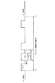
図2は、図1中の液晶パネル14の電気的構成の一例を示す図である。
この液晶パネル14は、同図2に示すように、バックライト16の光を入射させる透過型のものであり、同図2に示すように、データ電極Xi (i=1,2,…,m、たとえば、m=640×3)と、走査電極Yj (j=1,2,…,n、たとえば、n=480)と、画素領域20i,j とから構成されている。データ電極Xi は、x方向(すなわち、第1の方向)に所定間隔で設けられ、該当する表示信号Di が印加される。走査電極Yj は、x方向と直交するy方向(すなわち、走査方向、第2の方向)に所定間隔で設けられ、表示信号Di を書き込むための走査信号OUTj が線順次に印加される。画素領域20i,j は、データ電極Xi と走査電極Yj との交差領域と1対1に対応して設けられ、TFT(Thin Film Transistor、薄膜トランジスタ)21i,j と、液晶22i,j と、共通電極COMとから構成されている。TFT21i,j は、走査信号OUTj に基づいてオン/オフ制御され、オン状態になったときに液晶22i,j に表示信号Di を印加する。
FIG. 2 is a diagram illustrating an example of an electrical configuration of the
As shown in FIG. 2, the
この液晶パネル14では、走査電極Yj とデータ電極Xi とが駆動される、すなわち、走査電極Yj に走査信号OUTj が線順次に印加されると共にデータ電極Xi に該当する表示信号Di が書き込まれることにより、当該表示信号Di に対応する画素領域に所定の階調電圧が印加され、同液晶パネル14の液晶層を構成する液晶の応答が同階調電圧に基づいて制御されることにより、光の透過率が変化して表示画像が得られる。H−ドライバ12は、タイミングコントロール部25からの制御信号cta及び映像信号変換部22からの変換映像信号データfvrに基づいて、表示信号Di を液晶パネル14の各データ電極Xi に一括して印加する。V−ドライバ13は、タイミングコントロール部25からの制御信号ctbに基づいて、走査信号OUTj を液晶パネル14の各走査電極Yj に線順次に印加する。
In the
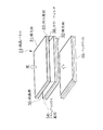
図3は、図1中の液晶パネル14の概略の構造及びバックライト16の位置を示す図である。
この液晶パネル14は、同図3に示すように、一対の偏光板31,32と、対向基板33と、アクティブマトリクス基板34と、これらの間に介挿された液晶層35とから構成されている。対向基板33上には、図2中の共通電極COMが設けられると共に、R,G,Bのカラーフィルタ36が形成され、R,G,Bの3色を有する3画素で1ドットが構成されている。アクティブマトリクス基板34は、図2中のTFT21i,j などの能動素子が設けられている。バックライト16は、液晶パネル14の裏面側に配置され、特に、この実施例では、図示しないR,G,BのLEDの光を面光源にするものであり、全体で液晶パネル14の表示画面とほぼ同一の大きさに形成されている。
FIG. 3 is a diagram showing a schematic structure of the
As shown in FIG. 3, the
この液晶パネル14では、バックライト16の白色光が、偏光板32を通過した後に直線偏光となって液晶層35に入射する。液晶層35は、たとえばTN(Twisted Nematic )型液晶で構成され、偏光の形状を変える働きをするが、この働きは液晶の配向状態によって決まっているため、表示信号Di に対応した階調電圧によって偏光形状が制御される。この液晶層35から出射する偏光の形状により、出射光が偏光板32に吸収されるか否かが決まる。このようにして、表示信号Di に対応した階調電圧によって光の透過率が制御される。また、カラーフィルタ36のR,G,Bの各画素を通過した光の加色混合によってカラー画像が得られる。
In the
図4は、図1中のバックライト16の要部を示す図である。
このバックライト16は、同図4に示すように、発光領域が液晶パネル14のy方向(第2の方向)に2分割され、LEDブロック16a,16bから構成されている。この場合、液晶パネル14に対する走査信号OUTj の書込み(印加)は、走査電極Yj の1ライン目からn(最終)ライン目の方向に線順次に行われるが、同バックライト16は、n/2ライン目の近傍で分割されている。バックライト16が、この例のように2分割されている場合、映像信号検出部21は、1,…,n/2ラインに対応したR,G,Bそれぞれの入力映像信号VDの最も明るい階調レベル、及び(n+1)/2,…,nラインに対応したR,G,Bそれぞれの入力映像信号VDの最も明るい階調レベルを検出する。
FIG. 4 is a diagram showing a main part of the
As shown in FIG. 4, the
図5は、図1の液晶表示装置の動作を説明するタイムチャート、及び図6が、同図5中のオン期間を時間軸方向に拡大した図である。
これらの図を参照して、この例の液晶表示装置に用いられる駆動方法の処理内容について説明する。
この液晶表示装置では、各LEDブロック16a,16bの発光領域に対応した液晶の応答に対応して同各LEDブロック16a,16bが所定の期間点灯し、かつ、同各LEDブロック16a,16bに対応して、入力映像信号VDのR,G,B毎の当該フレームにおける最も明るい階調レベルが検出され、同入力映像信号VDは、階調レベルの上限値を積算し、かつ上記最も明るい階調レベルで除算した値に変換される。そして、この値に対応した階調電圧が各データ電極に印加されると共に、同各LEDブロック16a,16bの点灯期間では、入力映像信号VDの階調レベルの上限値に対する上記最も明るい階調レベルの割合に比例したデューティで同各LEDブロック16a,16bが点滅する。
FIG. 5 is a time chart for explaining the operation of the liquid crystal display device of FIG. 1, and FIG. 6 is an enlarged view of the ON period in FIG. 5 in the time axis direction.
The processing contents of the driving method used in the liquid crystal display device of this example will be described with reference to these drawings.
In this liquid crystal display device, the LED blocks 16a and 16b are lit for a predetermined period corresponding to the response of the liquid crystal corresponding to the light emitting areas of the LED blocks 16a and 16b, and correspond to the LED blocks 16a and 16b. Then, the brightest gradation level in the corresponding frame for each of R, G, and B of the input video signal VD is detected, and the input video signal VD integrates the upper limit value of the gradation level, and the brightest gradation level. Converted to a value divided by level. A gradation voltage corresponding to this value is applied to each data electrode, and during the lighting period of each
すなわち、入力映像信号VDは、映像信号検出部21により、各LEDブロック16a,16bに対応して、R,G,B毎に、当該フレームにおける最も明るい階調レベルが検出され、同最も明るい階調レベルが最大階調データgrhとして映像信号変換部22及びLED輝度変換部23へ送出されると共に、同入力映像信号VDの1フレーム毎の映像信号fvjがフレームメモリ11に送出される。映像信号fvjは、フレームメモリ11に格納され、また、同フレームメモリ11から映像信号データfvqとして映像信号変換部22へ送出される。映像信号変換部22では、フレームメモリ11から送出された映像信号データfvqは、入力映像信号VDの階調レベルの上限値(64階調)を積算し、かつ最大階調データgrhで除算した値に変換され、同映像信号変換部22から変換映像信号データfvrとしてH−ドライバ12へ送出される。この場合、たとえば、最大階調データgrhが32階調のとき、映像信号変換部22では、32階調が64階調に変換され、10階調が20階調(=入力映像信号10階調×64階調/最大階調32階調)に変換される。
That is, in the input video signal VD, the brightest gradation level in the frame is detected by the video
また、タイミングコントロール部25では、入力されたタイミング信号tpに基づいて、制御信号ctaが生成されてH−ドライバ12に送出されると共に、制御信号ctbが生成されてV−ドライバ13に送出される。H−ドライバ12では、タイミングコントロール部25から送出された制御信号cta及び映像信号変換部22から送出された変換映像信号データfvrに基づいて表示信号Di が生成され、液晶パネル14へ送出される。V−ドライバ13では、タイミングコントロール部25から送出された制御信号ctbに基づいて走査信号OUTj が生成され、液晶パネル14へ送出される。液晶パネル14では、図示しない各走査電極Yj と各データ電極Xi とが駆動されることで、対応する画素領域に表示信号Di に対応した階調電圧が印加され、当該画素領域における液晶の応答が制御される。
The
一方、LED輝度変換部23では、各LEDブロック16a,16bの点灯期間で、入力映像信号VDの階調レベルの上限値に対する最大階調データgrhの割合に比例したデューティで同各LEDブロック16a,16bを点滅させるための制御信号ctuが生成され、同制御信号ctuが点灯タイミングコントロール部24へ出力される。たとえば、最大階調データgrhが32階調の場合、LEDブロック16a,16bの輝度が50%(最大階調データgrh;32階調/上限値;64階調)になるように制御信号ctuが生成される。点灯タイミングコントロール部24では、各LEDブロック16a,16bの発光領域に対応した液晶の応答に対応して同各LEDブロック16a,16bを制御信号ctuに基づいたデューティで点滅させるための制御信号ctvが生成され、同制御信号ctvがLEDドライバ15へ送出される。
On the other hand, in the LED
この場合、たとえば図5に示すように、LEDブロック16aの点灯期間T1(時刻t1乃至t2)は、iフレーム目(i;整数)のn/2ライン目の液晶が70%以上応答した時点から(i+1)フレーム目の1ライン目の液晶が30%以下の応答となる時点までの期間25%(固定)となっている。従って、点灯開始は時刻t1乃至t3の範囲、及び点灯終了が時刻t2乃至t4の範囲に入っていれば良い。同様に、LEDブロック16bの点灯期間T2は、iフレーム目のnライン目の液晶が70%以上応答した時点から(i+1)フレーム目のn/2ライン目の液晶が30%以下の応答となる時点までの期間25%(固定)となっている。
In this case, for example, as shown in FIG. 5, the lighting period T1 (time t1 to t2) of the
LEDドライバ15では、点灯タイミングコントロール部24から送出された制御信号ctvに基づいて、各LEDブロック16a,16bを点滅させるための駆動電圧dw1,dw2が生成される。LEDブロック16a,16bは、駆動電圧dw1,dw2が印加されることにより、たとえば図6に示すように、入力映像信号VDの階調レベルの上限値に対する最大階調データgrhの割合に比例したデューティで点滅する。たとえば、LEDブロック16a,16bの輝度が50%の場合、図6中の期間T2(時刻a1乃至c1)は、期間T3(時刻a1乃至b1)の50%となる。この場合、点灯期間T1は、1周期が時刻a1乃至b1の時間幅を有する2つ以上の周期で構成される。また、この実施例では、時刻a1乃至b1の期間及び点灯のタイミングは、所定の値に固定され、入力映像信号VDによって変化はしない。
The
以上のように、この第1の実施例では、各LEDブロック16a,16bの発光領域に対応した液晶の応答に対応して同各LEDブロック16a,16bが所定の期間点灯し、かつ、同各LEDブロック16a,16bに対応して、入力映像信号VDのR,G,B毎の当該フレームにおける最も明るい階調レベルが検出され、同入力映像信号VDは、階調レベルの上限値を積算し、かつ上記最も明るい階調レベルで除算した値に変換され、この値に対応した階調電圧が各データ電極に印加されると共に、同各LEDブロック16a,16bの点灯期間では、入力映像信号VDの階調レベルの上限値に対する上記最も明るい階調レベルの割合に比例したデューティで同各LEDブロック16a,16bが点滅するので、動画が表示されたときの尾引きが低減され、また、表示画面のコントラストが向上すると共に輝度のダイナミックレンジが向上する。また、入力映像信号VDによって各LEDブロック16a,16bの点灯デューティを変更する場合でも、各LEDブロック16a,16bの点灯タイミング及び点灯期間が固定され、かつ、同点灯期間が2つ以上の周期に分けられて同各LEDブロック16a,16bが点滅するので、階調レベルに関わらず、動画の尾引きが低減される。
As described above, in the first embodiment, the LED blocks 16a and 16b are turned on for a predetermined period in response to the response of the liquid crystal corresponding to the light emitting areas of the LED blocks 16a and 16b. Corresponding to the LED blocks 16a and 16b, the brightest gradation level in the corresponding frame for each of R, G and B of the input video signal VD is detected, and the input video signal VD integrates the upper limit value of the gradation level. And the gradation voltage corresponding to this value is applied to each data electrode, and the input video signal VD is applied during the lighting period of each
図7は、この発明の第2の実施例である液晶表示装置の電気的構成を示すブロック図であり、第1の実施例を示す図1中の要素と共通の要素には共通の符号が付されている。
この例の液晶表示装置では、同図7に示すように、図1中の駆動制御回路10に代えて、異なる構成の駆動制御回路10Aが設けられている。駆動制御回路10Aでは、図1中の映像信号検出部21に代えて、異なる機能を有する映像信号検出部21Aが設けられている。映像信号検出部21Aは、各LEDブロック16a,16bに対応して、入力映像信号VDのR,G,B毎に、当該フレームにおける最も明るい階調レベルを含む所定の範囲内の階調レベルの平均値を検出し、同平均値を最大階調データgrhとして映像信号変換部22及びLED輝度変換部23へ送出すると共に、入力映像信号VDの1フレーム毎の映像信号fvjをフレームメモリ11に送出する。また、上記平均値を最大階調データgrhとした場合、画素によっては本来の階調レベル(入力映像信号VDの階調レベル)より大きくなることがあるが、この画素の階調レベルに対しては、上限値に修正する。たとえば、上限値の64階調に対し、最大階調データgrhが65階調以上となる場合、同65階調を64階調に修正する。また、上記階調レベルの平均値は、たとえば、当該フレームにおける最も明るい階調レベルを有する画素を基準として、所定の範囲内の画素に対応した階調レベルを検出し、この検出結果の平均をとることにより求められる。この場合、たとえば、最も明るい階調レベルから上位10%以内の階調レベルの平均値、あるいは、最も明るい階調レベルを有する画素と周囲の画素との階調レベルの平均値などが用いられる。
FIG. 7 is a block diagram showing an electrical configuration of a liquid crystal display device according to a second embodiment of the present invention. Elements common to those in FIG. 1 showing the first embodiment are denoted by common reference numerals. It is attached.
In the liquid crystal display device of this example, as shown in FIG. 7, a drive control circuit 10A having a different configuration is provided in place of the drive control circuit 10 in FIG. In the drive control circuit 10A, a video
この液晶表示装置では、映像信号検出部21Aにより、入力映像信号VDのR,G,B毎に、当該フレームにおける最も明るい階調レベルを含む所定の範囲内の階調レベルの平均値が検出され、同平均値が最大階調データgrhとして出力される。このため、ある1画素のみの階調レベルが高い場合でも、表示画面全体のコントラストが向上すると共に輝度のダイナミックレンジが向上する。
In this liquid crystal display device, the average value of the gradation levels within a predetermined range including the brightest gradation level in the frame is detected by the video
図8は、この発明の第3の実施例である液晶表示装置の電気的構成を示すブロック図であり、第2の実施例を示す図7中の要素と共通の要素には共通の符号が付されている。
この例の液晶表示装置では、同図8に示すように、図7中の駆動制御回路10Aに代えて、異なる構成の駆動制御回路10Bが設けられると共に、フレームメモリ27が設けられている。駆動制御回路10Bでは、オーバードライブ部26が付加されている。フレームメモリ27は、映像信号変換部22から出力される変換映像信号データfvrを1フレーム毎に格納すると共に、変換映像信号データfvqaとしてオーバードライブ部26へ送出する。オーバードライブ部26は、映像信号変換部22から出力される変換映像信号データfvrの出力タイミングに同期して、フレームメモリ27から送出される変換映像信号データfvqaを、液晶パネル14の各画素領域20m,n に対して各フレーム期間毎にオーバードライブ駆動を行うためのレベルに変換して変換映像信号データfvraとしてH−ドライバ12へ送出する。
FIG. 8 is a block diagram showing an electrical configuration of a liquid crystal display device according to a third embodiment of the present invention. Elements common to those in FIG. 7 showing the second embodiment are denoted by common reference numerals. It is attached.
In the liquid crystal display device of this example, as shown in FIG. 8, a drive control circuit 10B having a different configuration is provided in place of the drive control circuit 10A in FIG. 7, and a
この液晶表示装置では、液晶パネル14の各画素領域20m,n に対して各フレーム期間毎にオーバードライブ駆動が行われるので、上記第2の実施例よりも液晶の応答が速くなり、動画の尾引きがさらに改善される。
In this liquid crystal display device, the overdrive drive is performed for each frame period of each
図9は、この発明の第4の実施例である液晶表示装置の電気的構成を示すブロック図である。
この例の液晶表示装置では、同図9に示すように、図8中の駆動制御回路10Bに代えて、異なる構成の駆動制御回路10Cが設けられている。駆動制御回路10Cでは、図8中の映像信号検出部21A、オーバードライブ部26及びタイミングコントロール部25に代えて、異なる機能を有する映像信号検出部21B、オーバードライブ部26A及びタイミングコントロール部25Aが設けられている。映像信号検出部21Bは、所定のフレーム周波数(たとえば、60Hz)で入力される入力映像信号VDの各フレームを同フレーム周波数の2倍(120Hz)のサブフレーム周波数を有する2個のサブフレーム(第1及び第2サブフレーム)に分割し、各サブフレーム毎に映像信号検出部21Aと同様の動作を行う機能を有している。
FIG. 9 is a block diagram showing an electrical configuration of a liquid crystal display device according to the fourth embodiment of the present invention.
In the liquid crystal display device of this example, as shown in FIG. 9, a drive control circuit 10C having a different configuration is provided instead of the drive control circuit 10B in FIG. In the drive control circuit 10C, instead of the video
オーバードライブ部26Aは、映像信号変換部22から出力される変換映像信号データfvrの出力タイミングに同期して、フレームメモリ27から送出される変換映像信号データfvqaを、液晶パネル14の各画素領域20m,n に対して第1サブフレームでオーバードライブ駆動を行うためのレベルに変換する一方、第2サブフレームで通常駆動を行うレベルとする。タイミングコントロール部25Aは、H−ドライバ12及びV−ドライバ13が上記第3の実施例の2倍の速度で動作するための制御信号cta及び制御信号ctbを出力する。なお、フレーム周波数は、液晶パネル14の規格が例えばXGA(Extended Graphics Array )の場合に60.00Hz、VGA(Video Graphics Array)の場合に59.94Hz、SVGA(Super Video Graphics Array)の場合に60.32Hzである。
The
この液晶表示装置では、図10に示すように、タイミングコントロール部25Aにより、H−ドライバ12及びV−ドライバ13が第3の実施例の2倍の速度で動作するため、各LEDブロック16a,16bの点滅時には、液晶の応答がさらに速くなり、動画の尾引きがさらに改善される。
In this liquid crystal display device, as shown in FIG. 10, the
図11は、この発明の第5の実施例である液晶表示装置の電気的構成を示すブロック図である。
この例の液晶表示装置では、同図11に示すように、図9中の駆動制御回路10Cに代えて、異なる構成の駆動制御回路10Dが設けられている。駆動制御回路10Dでは、図9中の映像信号検出部21B、オーバードライブ部26A、点灯タイミングコントロール部24及びタイミングコントロール部25Aに代えて、異なる機能を有する映像信号検出部21C、オーバードライブ部26B、点灯タイミングコントロール部24A及びタイミングコントロール部25Bが設けられている。映像信号検出部21Cは、入力映像信号VDの各フレームを同フレーム周波数の4倍(240Hz)のサブフレーム周波数を有する4個のサブフレーム(第1乃至第4サブフレーム)に分割し、各サブフレーム毎に図8中の映像信号検出部21Aと同様の動作を行う機能を有している。
FIG. 11 is a block diagram showing an electrical configuration of a liquid crystal display device according to the fifth embodiment of the present invention.
In the liquid crystal display device of this example, as shown in FIG. 11, a drive control circuit 10D having a different configuration is provided in place of the drive control circuit 10C in FIG. In the drive control circuit 10D, instead of the video
オーバードライブ部26Bは、映像信号変換部22から出力される変換映像信号データfvrの出力タイミングに同期して、フレームメモリ27から送出される変換映像信号データfvqaを、液晶パネル14の各画素領域20m,n に対して第1サブフレームでオーバードライブ駆動を行うためのレベルに変換する一方、第2乃至第4サブフレームで通常駆動を行うレベルとする。点灯タイミングコントロール部24Aは、フレーム期間中に、各LEDブロック16a,16bを所定の時間間隔で2回点灯させ、特に、この実施例では、点灯周波数を120Hzとする。タイミングコントロール部25Bは、H−ドライバ12及びV−ドライバ13が上記第3の実施例の4倍の速度で動作するための制御信号cta及び制御信号ctbを出力する。
The
この液晶表示装置では、図12に示すように、各LEDブロック16a,16bの点灯周波数が120Hzとなるため、同点灯周波数が60Hzの場合と比較して、ちらつきが視認されにくくなる。なお、第3乃至第4サブフレームでは、液晶に対する書込みを行わなくても良いが、次フレームの第1乃至第2サブフレームでは、液晶へ書き込む階調電圧の極性は、現フレームと反転させる。
In this liquid crystal display device, as shown in FIG. 12, since the lighting frequency of each
図13は、この発明の第6の実施例である液晶表示装置の電気的構成を示すブロック図である。
この例の液晶表示装置では、同図13に示すように、図8中の駆動制御回路10B、LEDドライバ15及びバックライト16に代えて、異なる構成の駆動制御回路10E、LEDドライバ15A及びバックライト16Aが設けられている。
FIG. 13 is a block diagram showing an electrical configuration of the liquid crystal display device according to the sixth embodiment of the present invention.
In the liquid crystal display device of this example, as shown in FIG. 13, instead of the drive control circuit 10B, the
図14は、図13中のバックライト16Aの要部を示す図である。
このバックライト16Aは、同図14に示すように、4行×4列に分割され、LEDブロック1A,1B,1C,1D,2A,2B,2C,2D,3A,3B,3C,3D,4A,4B,4C,4Dから構成されている。駆動制御回路10Eは、図8中の映像信号検出部21A、映像信号変換部22、LED輝度変換部23及び点灯タイミングコントロール部24に代えて、LEDドライバ15Aの各LEDブロックに対応して同様の動作をそれぞれ行う映像信号検出部21D、映像信号変換部22A、LED輝度変換部23A及び点灯タイミングコントロール部24Bが設けられている。LEDドライバ15Aは、点灯タイミングコントロール部24Bからの制御信号ctvに基づいて駆動電圧dw1,dw2,…,de16を生成し、上記各LEDブロックをそれぞれ駆動する。
FIG. 14 is a diagram showing a main part of the backlight 16A in FIG.
As shown in FIG. 14, the backlight 16A is divided into 4 rows × 4 columns, and LED blocks 1A, 1B, 1C, 1D, 2A, 2B, 2C, 2D, 3A, 3B, 3C, 3D, 4A. , 4B, 4C, 4D. The drive control circuit 10E corresponds to each LED block of the
この液晶表示装置では、上記第3の実施例における各LEDブロック16a,16bに対応した動作に代えて、LEDドライバ15Aの各LEDブロックに対応した動作が行われる。この場合、LEDドライバ15Aの各LEDブロックは、各行で同じ期間及び同じタイミングでオン状態となる。たとえば、LEDブロック1A,1B,1C,1Dは同時にオン状態となるが、同オン状態における点滅のデューティは、各LEDブロック1A,1B,1C,1D毎に制御される。また、映像信号変換部22Aから出力される変換映像信号データfvrも、LEDドライバ15Aの各LEDブロックに対応して、それぞれ出力される。このように、LEDドライバ15Aの各LEDブロックに対応する細分化した動作が行われるため、表示画面の解像度が向上する。
In this liquid crystal display device, an operation corresponding to each LED block of the
以上、この発明の実施例を図面により詳述してきたが、具体的な構成は同実施例に限られるものではなく、この発明の要旨を逸脱しない範囲の設計の変更などがあっても、この発明に含まれる。
たとえば、上記各実施例では、H−ドライバデータ12は、制御信号ctaに基づいて、入力映像信号VDに対応する表示信号Di を液晶パネル14の各データ電極Xi に一括して印加するが、同表示信号Di を各データ電極Xi に点順次に印加するようにしても良い。また、LEDブロック16a,16bの1回の点灯期間は、フレーム期間の12.5%に限定されない。また、図1中の液晶パネル14は、図2及び図3に示す構成に限定されず、たとえば、横型電界駆動(IPS、In-Plane Switching)方式によるものを用いても良い。また、上記実施例6以外の他の全ての実施例においても、図13中のバックライト16Aを用いて各LEDブロック毎に駆動する構成としても良い。また、バックライト16が複数のLEDブロックに分割されていない構成であっても、上記各実施例に準じた作用、効果が得られる。また、バックライト16,16Aは、R,G,BのLEDの他、たとえば深紅などのLEDを有していても良い。この場合、上記各実施例の駆動制御回路10,10A,10B,10C,10D,10Eも、同バックライト16,16Aの構成に対応したものとする必要がある。
The embodiment of the present invention has been described in detail with reference to the drawings. However, the specific configuration is not limited to the embodiment, and even if there is a design change without departing from the gist of the present invention, Included in the invention.
For example, in each of the above embodiments, the H-
この発明は、バックライトがLEDで構成され、たとえば液晶テレビなど、動画像を表示する液晶表示装置全般に適用できる。 The present invention can be applied to all liquid crystal display devices that display a moving image, such as a liquid crystal television set, and the like.
10,10A,10B,10C,10D,10E 駆動制御回路(駆動制御手段)
11 フレームメモリ(液晶表示装置の一部)
12 H−ドライバ(液晶表示装置の一部)
13 V−ドライバ(液晶表示装置の一部)
14 液晶パネル(液晶表示装置の一部)
15,15A LEDドライバ(液晶表示装置の一部)
16,16A バックライト(液晶表示装置の一部)
16a,16b LEDブロック(光源ブロック)
21,21A,21B,21C,21D 映像信号検出部(駆動制御手段の一部)
22,22A 映像信号変換部(駆動制御手段の一部)
23,23A LED輝度変換部(駆動制御手段の一部)
24,24A,24B 点灯タイミングコントロール部(駆動制御手段の一部)
25,25A,25B タイミングコントロール部(駆動制御手段の一部)
26,26A,26B オーバードライブ部(駆動制御手段の一部)
27 フレームメモリ
10, 10A, 10B, 10C, 10D, 10E Drive control circuit (drive control means)
11 Frame memory (part of liquid crystal display)
12 H-driver (part of liquid crystal display device)
13 V-driver (part of liquid crystal display device)
14 Liquid crystal panel (part of liquid crystal display device)
15,15A LED driver (part of liquid crystal display)
16,16A backlight (part of liquid crystal display)
16a, 16b LED block (light source block)
21, 21A, 21B, 21C, 21D Video signal detector (part of drive control means)
22, 22A Video signal converter (part of drive control means)
23, 23A LED luminance conversion unit (part of drive control means)
24, 24A, 24B lighting timing control section (part of drive control means)
25, 25A, 25B Timing control section (part of drive control means)
26, 26A, 26B Overdrive section (part of drive control means)
27 frame memory
Claims (15)
LEDドライバと、
少なくともR(赤),G(緑),B(青)のLEDを有し、前記LEDドライバの駆動電圧により前記液晶パネルを裏面側から照らすバックライトとを備え、該液晶パネルは、各走査電極と各データ電極とが駆動されることで、対応する画素領域に所定の階調電圧が印加され、該階調電圧に応じて当該画素領域における液晶の応答が制御されることにより入力映像信号に対応した表示画像を得る液晶表示装置であって、
前記R,G,B毎に階調レベルの上限値が設定されている前記入力映像信号の最も明るい階調レベルをフレーム毎、R,G,B毎に検出する映像信号検出部を有し、前記入力映像信号のフレーム期間中に、前記画素領域における前記所定の階調電圧の印加に対して液晶が応答する前は前記LEDドライバに前記バックライトを消灯させる一方、該応答した時点で該バックライトを所定の期間点灯させ、かつ、前記入力映像信号の階調レベルに、該当する前記上限値を積算し、かつ、前記映像信号検出部により検出されたフレーム毎、R,G,B毎の最も明るい階調レベルで除算した値に、前記入力映像信号の各階調レベルを変換すると共に、前記バックライトの点灯期間内では、前記上限値に対する前記最も明るい階調レベルの割合に対応したデューティで前記LEDドライバに該バックライトを点滅させる駆動制御手段が設けられていることを特徴とする液晶表示装置。 LCD panel,
An LED driver;
A backlight having at least R (red), G (green), and B (blue) LEDs, and illuminating the liquid crystal panel from the back side by the drive voltage of the LED driver, And each data electrode are driven, a predetermined gradation voltage is applied to the corresponding pixel area, and the response of the liquid crystal in the pixel area is controlled in accordance with the gradation voltage, whereby an input video signal is generated. A liquid crystal display device for obtaining a corresponding display image,
A video signal detection unit for detecting the brightest gray level of the input video signal in which an upper limit value of the gray level is set for each of R , G, and B, for each frame, for each of R , G, and B; Before the liquid crystal responds to the application of the predetermined gradation voltage in the pixel area during the frame period of the input video signal, the LED driver turns off the backlight, and at the time of the response, the backlight is turned off. The light is turned on for a predetermined period, and the corresponding upper limit value is added to the gradation level of the input video signal, and for each frame, R, G, and B detected by the video signal detector . the value obtained by dividing the brightest gradation level, converts the respective gradation levels of the input video signal, in the lighting period of the backlight corresponds to the ratio of the brightest gradation level for the upper limit A liquid crystal display device, characterized in that drive control means for causing the LED driver to blink the backlight with a high duty is provided.
LEDドライバと、
少なくともR(赤),G(緑),B(青)のLEDを有し、前記LEDドライバの駆動電圧により前記液晶パネルを裏面側から照らすバックライトとを備え、該液晶パネルは、各走査電極と各データ電極とが駆動されることで、対応する画素領域に所定の階調電圧が印加され、該階調電圧に応じて当該画素領域における液晶の応答が制御されることにより入力映像信号に対応した表示画像を得る液晶表示装置であって、
前記R,G,B毎に階調レベルの上限値が設定されている前記入力映像信号の最も明るい階調レベルを含む所定の範囲内の階調レベルの平均値をフレーム毎、R,G,B毎に検出する映像信号検出部を有し、前記入力映像信号のフレーム期間中に、前記画素領域における前記所定の階調電圧の印加に対して液晶が応答する前は前記LEDドライバに前記バックライトを消灯させる一方、該応答した時点で該バックライトを所定の期間点灯させ、かつ、前記入力映像信号の階調レベルに、該当する前記上限値を積算し、かつ、前記映像信号検出部により検出されたフレーム毎、R,G,B毎の前記平均値で除算した値に、前記入力映像信号の各階調レベルを変換すると共に、前記バックライトの点灯期間内では、前記上限値に対する前記平均値の割合に対応したデューティで前記LEDドライバに該バックライトを点滅させる駆動制御手段が設けられていることを特徴とする液晶表示装置。 LCD panel,
An LED driver;
A backlight having at least R (red), G (green), and B (blue) LEDs, and illuminating the liquid crystal panel from the back side by the drive voltage of the LED driver, And each data electrode are driven, a predetermined gradation voltage is applied to the corresponding pixel area, and the response of the liquid crystal in the pixel area is controlled in accordance with the gradation voltage, whereby an input video signal is generated. A liquid crystal display device for obtaining a corresponding display image,
An average value of gradation levels within a predetermined range including the brightest gradation level of the input video signal in which an upper limit value of gradation levels is set for each of R, G, and B is calculated for each frame, R 1 , G, A video signal detector for detecting each B, and before the liquid crystal responds to the application of the predetermined gradation voltage in the pixel area during the frame period of the input video signal, While turning off the light, when the response is made, the backlight is turned on for a predetermined period, and the corresponding upper limit value is added to the gradation level of the input video signal, and the video signal detection unit detected every frame, R, G, to a value above divided by the average value for each B, converts the respective gradation levels of the input video signal, in the lighting period of the backlight, the relative upper limit value Average value A drive control means for causing the LED driver to blink the backlight at a duty corresponding to the ratio is provided.
前記駆動制御手段は、
前記各光源ブロックの発光領域に対応した前記液晶の応答に対応して当該光源ブロックを所定の期間点灯させ、かつ、前記各光源ブロックに対応して、前記LEDドライバを制御することを特徴とする請求項1又は2記載の液晶表示装置。 The data electrodes of the liquid crystal panel are arranged in parallel with each other at a predetermined interval along a first direction, and the scan electrodes are spaced at a predetermined interval along a second direction orthogonal to the first direction. The backlights are arranged in parallel to each other, and the backlight has a light emitting region divided into m (m; an integer of 1 or more) in the first direction of the liquid crystal panel and k (k; an integer of 2 or more) in the second direction. It consists of a plurality of divided light source blocks,
The drive control means includes
The light source block is turned on for a predetermined period corresponding to the response of the liquid crystal corresponding to the light emitting area of each light source block, and the LED driver is controlled corresponding to each light source block. The liquid crystal display device according to claim 1 or 2.
当該フレームにおける最も明るい階調レベルを有する画素を基準として、所定の範囲内の画素に対応した階調レベルを検出し、この検出結果の平均をとることにより求めることを特徴とする請求項2記載の液晶表示装置。 The average value of the gradation levels is
3. The method according to claim 2 , wherein a gradation level corresponding to a pixel within a predetermined range is detected with reference to a pixel having the brightest gradation level in the frame, and an average of the detection results is obtained. Liquid crystal display device.
該液晶の応答がほぼ70%以上に達した第1の時点、あるいは、前記第1の時点以降の第2の時点に設定されていることを特徴とする請求項1乃至4のいずれか一に記載の液晶表示装置。 When the liquid crystal responds,
5. The first time point at which the response of the liquid crystal reaches approximately 70% or more, or a second time point after the first time point, is set. The liquid crystal display device described.
前記画素領域に対して、各フレーム期間中に、オーバードライブ駆動を行うことを特徴とする請求項1乃至5のいずれか一に記載の液晶表示装置。 The drive control means includes
The liquid crystal display device according to claim 1, wherein overdrive driving is performed on the pixel region during each frame period.
所定のフレーム周波数で入力される前記入力映像信号の各フレームを前記フレーム周波数のM倍(M;2以上の整数)のサブフレーム周波数を有するM個のサブフレームに分割し、対応する前記画素領域に対して、フレーム期間中に、第1番目の前記サブフレームでオーバードライブ駆動を行うと共に、第2番目以降の前記サブフレームで通常駆動を行うことを特徴とする請求項1乃至6のいずれか一に記載の液晶表示装置。 The drive control means includes
Each frame of the input video signal input at a predetermined frame frequency is divided into M subframes having a subframe frequency that is M times the frame frequency (M; an integer of 2 or more), and the corresponding pixel region On the other hand, during the frame period, overdrive driving is performed in the first subframe, and normal driving is performed in the second and subsequent subframes. The liquid crystal display device according to 1.
フレーム期間中に、前記バックライトを所定の時間間隔でN回(N;2以上の整数)点灯させることを特徴とする請求項1乃至7のいずれか一に記載の液晶表示装置。 The drive control means includes
8. The liquid crystal display device according to claim 1, wherein the backlight is turned on N times (N; an integer of 2 or more) at a predetermined time interval during a frame period.
LEDドライバと、
少なくともR(赤),G(緑),B(青)のLEDを有し、前記LEDドライバの駆動電圧により前記液晶パネルを裏面側から照らすバックライトとを備え、該液晶パネルは、各走査電極と各データ電極とが駆動されることで、対応する画素領域に所定の階調電圧が印加され、該階調電圧に応じて当該画素領域における液晶の応答が制御されることにより入力映像信号に対応した表示画像を得る液晶表示装置に用いられる駆動制御回路であって、
前記R,G,B毎に階調レベルの上限値が設定されている前記入力映像信号の最も明るい階調レベルをフレーム毎、R,G,B毎に検出する映像信号検出部を有し、前記入力映像信号のフレーム期間中に、前記画素領域における前記所定の階調電圧の印加に対して液晶が応答する前は前記LEDドライバに前記バックライトを消灯させる一方、該応答した時点で該バックライトを所定の期間点灯させ、かつ、前記入力映像信号の階調レベルに、該当する前記上限値を積算し、かつ、前記映像信号検出部により検出されたフレーム毎、R,G,B毎の最も明るい階調レベルで除算した値に、前記入力映像信号の各階調レベルを変換すると共に、前記バックライトの点灯期間内では、前記上限値に対する前記最も明るい階調レベルの割合に対応したデューティで前記LEDドライバに該バックライトを点滅させることを特徴とする液晶表示装置に用いられる駆動制御回路。 LCD panel,
An LED driver;
A backlight having at least R (red), G (green), and B (blue) LEDs, and illuminating the liquid crystal panel from the back side by the drive voltage of the LED driver, And each data electrode are driven, a predetermined gradation voltage is applied to the corresponding pixel area, and the response of the liquid crystal in the pixel area is controlled in accordance with the gradation voltage, whereby an input video signal is generated. A drive control circuit used in a liquid crystal display device for obtaining a corresponding display image,
A video signal detection unit for detecting the brightest gray level of the input video signal in which an upper limit value of the gray level is set for each of R , G, and B, for each frame, for each of R , G, and B; Before the liquid crystal responds to the application of the predetermined gradation voltage in the pixel area during the frame period of the input video signal, the LED driver turns off the backlight, and at the time of the response, the backlight is turned off. The light is turned on for a predetermined period, and the corresponding upper limit value is added to the gradation level of the input video signal, and for each frame, R, G, and B detected by the video signal detector . the value obtained by dividing the brightest gradation level, converts the respective gradation levels of the input video signal, in the lighting period of the backlight corresponds to the ratio of the brightest gradation level for the upper limit A drive control circuit for use in a liquid crystal display device, wherein the LED driver causes the backlight to blink at a high duty.
LEDドライバと、
少なくともR(赤),G(緑),B(青)のLEDを有し、前記LEDドライバの駆動電圧により前記液晶パネルを裏面側から照らすバックライトとを備え、該液晶パネルは、各走査電極と各データ電極とが駆動されることで、対応する画素領域に所定の階調電圧が印加され、該階調電圧に応じて当該画素領域における液晶の応答が制御されることにより入力映像信号に対応した表示画像を得る液晶表示装置に用いられる駆動制御回路であって、
前記R,G,B毎に階調レベルの上限値が設定されている前記入力映像信号の最も明るい階調レベルを含む所定の範囲内の階調レベルの平均値をフレーム毎、R,G,B毎に検出する映像信号検出部を有し、前記入力映像信号のフレーム期間中に、前記画素領域における前記所定の階調電圧の印加に対して液晶が応答する前は前記LEDドライバに前記バックライトを消灯させる一方、該応答した時点で該バックライトを所定の期間点灯させ、かつ、前記入力映像信号の階調レベルに、該当する前記上限値を積算し、かつ、前記映像信号検出部により検出されたフレーム毎、R,G,B毎の前記平均値で除算した値に、前記入力映像信号の各階調レベルを変換すると共に、前記バックライトの点灯期間内では、前記上限値に対する前記平均値の割合に対応したデューティで前記LEDドライバに該バックライトを点滅させることを特徴とする液晶表示装置に用いられる駆動制御回路。 LCD panel,
An LED driver;
A backlight having at least R (red), G (green), and B (blue) LEDs, and illuminating the liquid crystal panel from the back side by the drive voltage of the LED driver, And each data electrode are driven, a predetermined gradation voltage is applied to the corresponding pixel area, and the response of the liquid crystal in the pixel area is controlled in accordance with the gradation voltage, whereby an input video signal is generated. A drive control circuit used in a liquid crystal display device for obtaining a corresponding display image,
An average value of gradation levels within a predetermined range including the brightest gradation level of the input video signal in which an upper limit value of gradation levels is set for each of R, G, and B is calculated for each frame, R 1 , G, A video signal detector for detecting each B, and before the liquid crystal responds to the application of the predetermined gradation voltage in the pixel area during the frame period of the input video signal, While turning off the light, when the response is made, the backlight is turned on for a predetermined period, and the corresponding upper limit value is added to the gradation level of the input video signal, and the video signal detection unit detected every frame, R, G, to a value above divided by the average value for each B, converts the respective gradation levels of the input video signal, in the lighting period of the backlight, the relative upper limit value Average value A drive control circuit for use in a liquid crystal display device, wherein the LED driver causes the backlight to blink at a duty corresponding to the ratio of.
前記各光源ブロックの発光領域に対応した前記液晶の応答に対応して当該光源ブロックを所定の期間点灯させ、かつ、前記各光源ブロックに対応して、前記LEDドライバを制御することを特徴とする請求項9又は10記載の液晶表示装置に用いられる駆動制御回路。 The data electrodes of the liquid crystal panel are arranged in parallel with each other at a predetermined interval along a first direction, and the scan electrodes are spaced at a predetermined interval along a second direction orthogonal to the first direction. The backlights are arranged in parallel to each other, and the backlight has a light emitting region divided into m (m; an integer of 1 or more) in the first direction of the liquid crystal panel and k (k; an integer of 2 or more) in the second direction. It consists of a plurality of divided light source blocks,
The light source block is turned on for a predetermined period corresponding to the response of the liquid crystal corresponding to the light emitting area of each light source block, and the LED driver is controlled corresponding to each light source block. The drive control circuit used for the liquid crystal display device of Claim 9 or 10.
LEDドライバと、
少なくともR(赤),G(緑),B(青)のLEDを有し、前記LEDドライバの駆動電圧により前記液晶パネルを裏面側から照らすバックライトとを備え、該液晶パネルは、各走査電極と各データ電極とが駆動されることで、対応する画素領域に所定の階調電圧が印加され、該階調電圧に応じて当該画素領域における液晶の応答が制御されることにより入力映像信号に対応した表示画像を得る液晶表示装置に用いられる駆動方法であって、
駆動制御手段に、前記R,G,B毎に階調レベルの上限値が設定されている前記入力映像信号の最も明るい階調レベルをフレーム毎、R,G,B毎に検出する映像信号検出部を設け、該駆動制御手段が、前記入力映像信号のフレーム期間中に、前記画素領域における前記所定の階調電圧の印加に対して液晶が応答する前は前記LEDドライバに前記バックライトを消灯させる一方、該応答した時点で該バックライトを所定の期間点灯させ、かつ、前記入力映像信号の階調レベルに、該当する前記上限値を積算し、かつ、前記映像信号検出部により検出されたフレーム毎、R,G,B毎の最も明るい階調レベルで除算した値に、前記入力映像信号の各階調レベルを変換すると共に、前記バックライトの点灯期間内では、前記上限値に対する前記最も明るい階調レベルの割合に対応したデューティで前記LEDドライバに該バックライトを点滅させることを特徴とする液晶表示装置に用いられる駆動方法。 LCD panel,
An LED driver;
A backlight having at least R (red), G (green), and B (blue) LEDs, and illuminating the liquid crystal panel from the back side by the drive voltage of the LED driver, And each data electrode are driven, a predetermined gradation voltage is applied to the corresponding pixel area, and the response of the liquid crystal in the pixel area is controlled in accordance with the gradation voltage, whereby an input video signal is generated. A driving method used in a liquid crystal display device for obtaining a corresponding display image,
Video signal detection for detecting the brightest gradation level of the input video signal for each frame, R , G, and B for which the upper limit value of the gradation level is set for each of R, G, and B in the drive control means And the drive control means turns off the backlight to the LED driver before the liquid crystal responds to the application of the predetermined gradation voltage in the pixel area during the frame period of the input video signal. On the other hand, when the response is made, the backlight is turned on for a predetermined period, and the corresponding upper limit value is added to the gradation level of the input video signal, and detected by the video signal detection unit every frame, R, G, the value obtained by dividing the brightest gradation level for each B, converts the respective gradation levels of the input video signal, in the lighting period of the backlight, the relative upper limit value A driving method used for a liquid crystal display device, wherein the LED driver is caused to blink the backlight with a duty corresponding to a ratio of the brightest gradation level.
LEDドライバと、
少なくともR(赤),G(緑),B(青)のLEDを有し、前記LEDドライバの駆動電圧により前記液晶パネルを裏面側から照らすバックライトとを備え、該液晶パネルは、各走査電極と各データ電極とが駆動されることで、対応する画素領域に所定の階調電圧が印加され、該階調電圧に応じて当該画素領域における液晶の応答が制御されることにより入力映像信号に対応した表示画像を得る液晶表示装置に用いられる駆動方法であって、
駆動制御手段に、前記R,G,B毎に階調レベルの上限値が設定されている前記入力映像信号の最も明るい階調レベルを含む所定の範囲内の階調レベルの平均値をフレーム毎、R,G,B毎に検出する映像信号検出部を設け、該駆動制御手段が、前記入力映像信号のフレーム期間中に、前記画素領域における前記所定の階調電圧の印加に対して液晶が応答する前は前記LEDドライバに前記バックライトを消灯させる一方、該応答した時点で該バックライトを所定の期間点灯させ、かつ、前記入力映像信号の階調レベルに、該当する前記上限値を積算し、かつ、前記映像信号検出部により検出されたフレーム毎、R,G,B毎の前記平均値で除算した値に、前記入力映像信号の各階調レベルを変換すると共に、前記バックライトの点灯期間内では、前記上限値に対する前記平均値の割合に対応したデューティで前記LEDドライバに該バックライトを点滅させることを特徴とする液晶表示装置に用いられる駆動方法。 LCD panel,
An LED driver;
A backlight having at least R (red), G (green), and B (blue) LEDs, and illuminating the liquid crystal panel from the back side by the drive voltage of the LED driver, And each data electrode are driven, a predetermined gradation voltage is applied to the corresponding pixel area, and the response of the liquid crystal in the pixel area is controlled in accordance with the gradation voltage, whereby an input video signal is generated. A driving method used in a liquid crystal display device for obtaining a corresponding display image,
An average value of gradation levels within a predetermined range including the brightest gradation level of the input video signal in which an upper limit value of gradation levels is set for each of R, G, and B is supplied to the drive control means for each frame. , R 1 , G, and B for detecting a video signal detecting unit, and the drive control means is configured to cause the liquid crystal to respond to the application of the predetermined gradation voltage in the pixel region during the frame period of the input video signal. Before responding, the LED driver is made to turn off the backlight, and when the response is made, the backlight is turned on for a predetermined period, and the corresponding upper limit value is integrated with the gradation level of the input video signal. and, and, for each frame detected by the video signal detection unit, R, G, to a value obtained by dividing the average value for each B, it converts the respective gradation levels of the input video signal, the backlight Within lighting period Then, a driving method used for a liquid crystal display device, wherein the LED driver blinks the backlight with a duty corresponding to a ratio of the average value to the upper limit value.
前記駆動制御手段が、前記各光源ブロックの発光領域に対応した前記液晶の応答に対応して当該光源ブロックを所定の期間点灯させ、かつ、前記各光源ブロックに対応して、前記LEDドライバを制御することを特徴とする請求項13又は14記載の液晶表示装置に用いられる駆動方法。 The data electrodes of the liquid crystal panel are arranged in parallel with each other at a predetermined interval along a first direction, and the scan electrodes are spaced at a predetermined interval along a second direction orthogonal to the first direction. The backlights are arranged in parallel to each other, and the backlight has a light emitting region divided into m (m; an integer of 1 or more) in the first direction of the liquid crystal panel and k (k; an integer of 2 or more) in the second direction. It consists of a plurality of divided light source blocks,
The drive control means turns on the light source block for a predetermined period corresponding to the response of the liquid crystal corresponding to the light emitting area of each light source block, and controls the LED driver corresponding to each light source block The drive method used for the liquid crystal display device of Claim 13 or 14 characterized by the above-mentioned.
Priority Applications (3)
| Application Number | Priority Date | Filing Date | Title |
|---|---|---|---|
| JP2006189352A JP5256552B2 (en) | 2006-07-10 | 2006-07-10 | Liquid crystal display device, drive control circuit used for the liquid crystal display device, and drive method |
| US11/775,009 US7952556B2 (en) | 2006-07-10 | 2007-07-09 | Liquid crystal display device, driving control circuit and driving method used in same device |
| CN2007101283633A CN101105920B (en) | 2006-07-10 | 2007-07-10 | Liquid crystal display device, driving control circuit and driving method used in same device |
Applications Claiming Priority (1)
| Application Number | Priority Date | Filing Date | Title |
|---|---|---|---|
| JP2006189352A JP5256552B2 (en) | 2006-07-10 | 2006-07-10 | Liquid crystal display device, drive control circuit used for the liquid crystal display device, and drive method |
Related Child Applications (1)
| Application Number | Title | Priority Date | Filing Date |
|---|---|---|---|
| JP2012230373A Division JP2013020269A (en) | 2012-10-17 | 2012-10-17 | Liquid crystal display device, drive control circuit used in the liquid crystal display device and drive method |
Publications (3)
| Publication Number | Publication Date |
|---|---|
| JP2008015430A JP2008015430A (en) | 2008-01-24 |
| JP2008015430A5 JP2008015430A5 (en) | 2009-06-04 |
| JP5256552B2 true JP5256552B2 (en) | 2013-08-07 |
Family
ID=38918705
Family Applications (1)
| Application Number | Title | Priority Date | Filing Date |
|---|---|---|---|
| JP2006189352A Active JP5256552B2 (en) | 2006-07-10 | 2006-07-10 | Liquid crystal display device, drive control circuit used for the liquid crystal display device, and drive method |
Country Status (3)
| Country | Link |
|---|---|
| US (1) | US7952556B2 (en) |
| JP (1) | JP5256552B2 (en) |
| CN (1) | CN101105920B (en) |
Families Citing this family (51)
| Publication number | Priority date | Publication date | Assignee | Title |
|---|---|---|---|---|
| JP5110355B2 (en) * | 2007-07-09 | 2012-12-26 | Nltテクノロジー株式会社 | Backlight driving method and apparatus for liquid crystal display device, and liquid crystal display device |
| US8508522B2 (en) * | 2007-09-12 | 2013-08-13 | Rochester Institute Of Technology | Derivative sampled, fast settling time current driver |
| KR101588328B1 (en) * | 2007-10-30 | 2016-01-26 | 삼성디스플레이 주식회사 | Liquid crystal display and driving method of the same |
| TWI394127B (en) * | 2007-12-10 | 2013-04-21 | 友達光電股份有限公司 | Method of generating control signal for compression response time |
| JP2009175627A (en) * | 2008-01-28 | 2009-08-06 | Seiko Epson Corp | Image display device and electronic apparatus |
| US8493313B2 (en) * | 2008-02-13 | 2013-07-23 | Dolby Laboratories Licensing Corporation | Temporal filtering of video signals |
| TWI406261B (en) * | 2008-07-03 | 2013-08-21 | Cpt Technology Group Co Ltd | Driving method of liquid crystal display |
| KR101483627B1 (en) * | 2008-07-29 | 2015-01-19 | 삼성디스플레이 주식회사 | Display device |
| RU2469417C1 (en) * | 2008-10-10 | 2012-12-10 | Шарп Кабусики Кайся | Image display device |
| JP2010145509A (en) * | 2008-12-16 | 2010-07-01 | Epson Imaging Devices Corp | Liquid crystal display, its driving method, and electronic appliance |
| KR101318754B1 (en) * | 2008-12-16 | 2013-10-16 | 엘지디스플레이 주식회사 | Liquid Crystal Display Device |
| KR101318755B1 (en) * | 2008-12-18 | 2013-10-16 | 엘지디스플레이 주식회사 | Liquid Crystal Display Device |
| CN101794559B (en) * | 2009-02-03 | 2013-03-20 | 乐金显示有限公司 | Backlight assembly of liquid crystal display device |
| JP2010197548A (en) * | 2009-02-24 | 2010-09-09 | Victor Co Of Japan Ltd | Image display device |
| KR101598393B1 (en) | 2009-06-08 | 2016-03-02 | 삼성디스플레이 주식회사 | Method of dimming light source, display device for performing the same |
| JP2011059177A (en) | 2009-09-07 | 2011-03-24 | Hitachi Consumer Electronics Co Ltd | Liquid crystal display device and backlight control method |
| JP5335653B2 (en) | 2009-12-04 | 2013-11-06 | ミツミ電機株式会社 | Liquid crystal display device and liquid crystal display method |
| JP2011118278A (en) * | 2009-12-07 | 2011-06-16 | Panasonic Corp | Backlight device and video display device using the same |
| KR101633114B1 (en) * | 2009-12-11 | 2016-06-23 | 엘지디스플레이 주식회사 | Liquid crystal display and picture quality controlling method thereof |
| JP5381804B2 (en) * | 2010-02-25 | 2014-01-08 | セイコーエプソン株式会社 | Video processing circuit, video processing method, liquid crystal display device, and electronic apparatus |
| JP5556234B2 (en) * | 2010-02-25 | 2014-07-23 | セイコーエプソン株式会社 | VIDEO PROCESSING CIRCUIT, ITS PROCESSING METHOD, LIQUID CRYSTAL DISPLAY DEVICE, AND ELECTRONIC DEVICE |
| JP5267496B2 (en) * | 2010-04-05 | 2013-08-21 | 株式会社Jvcケンウッド | Liquid crystal display device and video display method used therefor |
| JP5661336B2 (en) | 2010-05-28 | 2015-01-28 | 日立マクセル株式会社 | Liquid crystal display |
| KR101761542B1 (en) * | 2010-10-08 | 2017-07-27 | 엘지디스플레이 주식회사 | Liquid crystal display device and driving method thereof |
| JP5720221B2 (en) | 2010-12-13 | 2015-05-20 | セイコーエプソン株式会社 | Video processing method, video processing circuit, liquid crystal display device, and electronic apparatus |
| CN102737585A (en) * | 2011-04-06 | 2012-10-17 | 中兴通讯股份有限公司 | Method for reducing backlight power consumption of display device and apparatus thereof |
| KR20120132912A (en) * | 2011-05-30 | 2012-12-10 | 삼성전자주식회사 | Apparatus For Multi-Mode Displaying And Driving Method thereof |
| JP5124051B1 (en) * | 2012-03-02 | 2013-01-23 | シャープ株式会社 | Display device |
| US9607556B2 (en) | 2012-06-15 | 2017-03-28 | Dolby Laboratories Licensing Corporation | Systems and methods for controlling dual modulation displays |
| US8988574B2 (en) | 2012-12-27 | 2015-03-24 | Panasonic Intellectual Property Corporation Of America | Information communication method for obtaining information using bright line image |
| US9560284B2 (en) | 2012-12-27 | 2017-01-31 | Panasonic Intellectual Property Corporation Of America | Information communication method for obtaining information specified by striped pattern of bright lines |
| US9088360B2 (en) | 2012-12-27 | 2015-07-21 | Panasonic Intellectual Property Corporation Of America | Information communication method |
| US9608725B2 (en) | 2012-12-27 | 2017-03-28 | Panasonic Intellectual Property Corporation Of America | Information processing program, reception program, and information processing apparatus |
| US10303945B2 (en) | 2012-12-27 | 2019-05-28 | Panasonic Intellectual Property Corporation Of America | Display method and display apparatus |
| US10530486B2 (en) | 2012-12-27 | 2020-01-07 | Panasonic Intellectual Property Corporation Of America | Transmitting method, transmitting apparatus, and program |
| US8922666B2 (en) | 2012-12-27 | 2014-12-30 | Panasonic Intellectual Property Corporation Of America | Information communication method |
| US9608727B2 (en) | 2012-12-27 | 2017-03-28 | Panasonic Intellectual Property Corporation Of America | Switched pixel visible light transmitting method, apparatus and program |
| US9087349B2 (en) | 2012-12-27 | 2015-07-21 | Panasonic Intellectual Property Corporation Of America | Information communication method |
| CN104871454B (en) | 2012-12-27 | 2018-09-28 | 松下电器(美国)知识产权公司 | Information communicating method and information-communication device |
| EP2940893B1 (en) | 2012-12-27 | 2021-05-19 | Panasonic Intellectual Property Corporation of America | Information communication method |
| CN104871452B (en) * | 2012-12-27 | 2018-04-27 | 松下电器(美国)知识产权公司 | Visual optical communication method and visual optical communication apparatus |
| US10523876B2 (en) | 2012-12-27 | 2019-12-31 | Panasonic Intellectual Property Corporation Of America | Information communication method |
| US10951310B2 (en) | 2012-12-27 | 2021-03-16 | Panasonic Intellectual Property Corporation Of America | Communication method, communication device, and transmitter |
| US9247180B2 (en) | 2012-12-27 | 2016-01-26 | Panasonic Intellectual Property Corporation Of America | Video display method using visible light communication image including stripe patterns having different pitches |
| US10163408B1 (en) * | 2014-09-05 | 2018-12-25 | Pixelworks, Inc. | LCD image compensation for LED backlighting |
| CN104505055B (en) * | 2014-12-31 | 2017-02-22 | 深圳创维-Rgb电子有限公司 | Method and device for adjusting backlight brightness |
| US10460641B2 (en) * | 2015-05-28 | 2019-10-29 | Lg Display Co., Ltd. | Image processing circuit and display device using the histogram analyzer to perform a differential shift and extension shift of image data gray level to adjust gray level respect to the brightness image level |
| CN106855679B (en) * | 2015-12-08 | 2019-05-03 | 深圳光峰科技股份有限公司 | Projection arrangement and its control method |
| US10902798B2 (en) | 2017-07-21 | 2021-01-26 | Hewlett-Packard Development Company, L.P. | Inactive state backlights |
| CN107481673B (en) * | 2017-08-14 | 2019-11-08 | 上海天马有机发光显示技术有限公司 | An organic light-emitting display panel and its driving method and driving device |
| CN115083339B (en) * | 2022-07-26 | 2023-01-03 | 惠科股份有限公司 | Driving method and driving device of display panel |
Family Cites Families (23)
| Publication number | Priority date | Publication date | Assignee | Title |
|---|---|---|---|---|
| US4978526A (en) * | 1988-09-26 | 1990-12-18 | Inolex Chemical Company | Hair and skin conditioning agents and methods |
| JP3402602B2 (en) * | 2000-12-22 | 2003-05-06 | 株式会社ヒューネット | Liquid crystal driving device and gradation display method |
| US6762742B2 (en) * | 2000-12-29 | 2004-07-13 | Samsung Electronics Co., Ltd. | Apparatus and method for automatic brightness control for use in liquid crystal display device |
| TW502234B (en) * | 2001-05-21 | 2002-09-11 | Chi Mei Optoelectronics Corp | Sub-frame driving method |
| CN101241684A (en) * | 2001-11-02 | 2008-08-13 | 夏普株式会社 | image display device |
| JP3732775B2 (en) * | 2001-11-08 | 2006-01-11 | 株式会社東芝 | Liquid crystal display device and driving method of liquid crystal display device |
| JP4167474B2 (en) * | 2002-11-07 | 2008-10-15 | シャープ株式会社 | Liquid crystal display |
| JP4371765B2 (en) * | 2003-10-17 | 2009-11-25 | Nec液晶テクノロジー株式会社 | Liquid crystal display |
| KR100570966B1 (en) * | 2003-11-17 | 2006-04-14 | 엘지.필립스 엘시디 주식회사 | Driving Method and Driving Device of Liquid Crystal Display |
| US7375719B2 (en) * | 2003-12-29 | 2008-05-20 | Lg. Philips Lcd. Co., Ltd | Method and apparatus for driving liquid crystal display |
| JP4612406B2 (en) | 2004-02-09 | 2011-01-12 | 株式会社日立製作所 | Liquid crystal display device |
| JP2005241677A (en) * | 2004-02-24 | 2005-09-08 | Matsushita Electric Ind Co Ltd | Display device and display method |
| KR100619627B1 (en) * | 2004-05-27 | 2006-09-08 | 엘지.필립스 엘시디 주식회사 | Luminance Control Device and Method of Liquid Crystal Display |
| KR101096720B1 (en) * | 2004-05-28 | 2011-12-22 | 엘지디스플레이 주식회사 | Apparatus and method for driving liquid crystal display device |
| JP4508754B2 (en) * | 2004-07-14 | 2010-07-21 | 三菱電機株式会社 | Image display device and image display method |
| JP2006030783A (en) * | 2004-07-20 | 2006-02-02 | Alps Electric Co Ltd | Liquid crystal display device |
| JP2005122121A (en) * | 2004-08-12 | 2005-05-12 | Hitachi Ltd | Liquid crystal display |
| WO2006038253A1 (en) * | 2004-09-30 | 2006-04-13 | Fujitsu Limited | Liquid crystal display device |
| US20070257873A1 (en) * | 2004-10-04 | 2007-11-08 | Koninklijke Philips Electronics, N.V. | Brightness control of a lighting unit of a matrix display device |
| KR101097584B1 (en) * | 2004-11-25 | 2011-12-22 | 엘지디스플레이 주식회사 | Apparatus and method for luminance control of liquid crystal display device |
| KR101460089B1 (en) * | 2004-12-23 | 2014-11-10 | 돌비 레버러토리즈 라이쎈싱 코오포레이션 | Wide color gamut display, and apparatus and method for displaying images at a viewing area |
| KR101136185B1 (en) * | 2004-12-30 | 2012-04-17 | 엘지디스플레이 주식회사 | Liquid Crystal Display device and method for driving the same |
| JP2006189661A (en) * | 2005-01-06 | 2006-07-20 | Toshiba Corp | Image display apparatus and method |
-
2006
- 2006-07-10 JP JP2006189352A patent/JP5256552B2/en active Active
-
2007
- 2007-07-09 US US11/775,009 patent/US7952556B2/en active Active
- 2007-07-10 CN CN2007101283633A patent/CN101105920B/en active Active
Also Published As
| Publication number | Publication date |
|---|---|
| US20080007512A1 (en) | 2008-01-10 |
| CN101105920A (en) | 2008-01-16 |
| JP2008015430A (en) | 2008-01-24 |
| CN101105920B (en) | 2011-08-10 |
| US7952556B2 (en) | 2011-05-31 |
Similar Documents
| Publication | Publication Date | Title |
|---|---|---|
| JP5256552B2 (en) | Liquid crystal display device, drive control circuit used for the liquid crystal display device, and drive method | |
| JP4997623B2 (en) | Liquid crystal display device, drive control circuit used for the liquid crystal display device, and drive method | |
| US7336325B2 (en) | Liquid crystal display and method and apparatus for driving the same comprising of color filters and colored backlights | |
| US7505016B2 (en) | Apparatus and method for driving liquid crystal display device | |
| US8648883B2 (en) | Display apparatus and method of driving the same | |
| JP2006084710A (en) | Display control circuit, display control method, and liquid crystal display | |
| JP5662960B2 (en) | Liquid crystal display device and driving method thereof | |
| CN101436391A (en) | Liquid crystal display device and method of driving same | |
| KR20160084547A (en) | Curved liquid crystal display | |
| KR100612304B1 (en) | LCD and its driving method | |
| US20090174730A1 (en) | Data driving apparatus and method thereof | |
| KR101323523B1 (en) | Liquid crystal display and driving method thereof | |
| JP2013020269A (en) | Liquid crystal display device, drive control circuit used in the liquid crystal display device and drive method | |
| KR101314212B1 (en) | Scanning backlight type Liquid Crystal Display Device and driving method of the same | |
| JP2007206326A (en) | Liquid crystal display device, driving circuit and driving method used for the liquid crystal display device | |
| KR20100131742A (en) | Light emitting device and driving method thereof | |
| KR101365896B1 (en) | Liquid crystal display device and method driving of the same | |
| JP2006085009A (en) | Display control circuit, display control method, and liquid crystal display | |
| KR100965823B1 (en) | Driving method of liquid crystal display device to minimize afterimage and device therefor | |
| KR102323772B1 (en) | Liquid crystal display device | |
| KR101521661B1 (en) | Backlight unit and liquid crystal display device having the same | |
| KR100612337B1 (en) | Thin film transistor liquid crystal display device and driving method thereof | |
| KR101728782B1 (en) | liquid crystal display device and method of driving the same | |
| KR20150113267A (en) | Liquid crystal display device | |
| JP5194735B2 (en) | Electro-optical device, driving method thereof, and electronic apparatus |
Legal Events
| Date | Code | Title | Description |
|---|---|---|---|
| A521 | Request for written amendment filed |
Free format text: JAPANESE INTERMEDIATE CODE: A523 Effective date: 20090420 |
|
| A621 | Written request for application examination |
Free format text: JAPANESE INTERMEDIATE CODE: A621 Effective date: 20090611 |
|
| A131 | Notification of reasons for refusal |
Free format text: JAPANESE INTERMEDIATE CODE: A131 Effective date: 20120117 |
|
| A521 | Request for written amendment filed |
Free format text: JAPANESE INTERMEDIATE CODE: A523 Effective date: 20120319 |
|
| A131 | Notification of reasons for refusal |
Free format text: JAPANESE INTERMEDIATE CODE: A131 Effective date: 20120417 |
|
| A521 | Request for written amendment filed |
Free format text: JAPANESE INTERMEDIATE CODE: A523 Effective date: 20120618 |
|
| A02 | Decision of refusal |
Free format text: JAPANESE INTERMEDIATE CODE: A02 Effective date: 20120717 |
|
| A521 | Request for written amendment filed |
Free format text: JAPANESE INTERMEDIATE CODE: A523 Effective date: 20121017 |
|
| A911 | Transfer to examiner for re-examination before appeal (zenchi) |
Free format text: JAPANESE INTERMEDIATE CODE: A911 Effective date: 20121024 |
|
| TRDD | Decision of grant or rejection written | ||
| A01 | Written decision to grant a patent or to grant a registration (utility model) |
Free format text: JAPANESE INTERMEDIATE CODE: A01 Effective date: 20130319 |
|
| A61 | First payment of annual fees (during grant procedure) |
Free format text: JAPANESE INTERMEDIATE CODE: A61 Effective date: 20130405 |
|
| FPAY | Renewal fee payment (event date is renewal date of database) |
Free format text: PAYMENT UNTIL: 20160502 Year of fee payment: 3 |
|
| R150 | Certificate of patent or registration of utility model |
Ref document number: 5256552 Country of ref document: JP Free format text: JAPANESE INTERMEDIATE CODE: R150 Free format text: JAPANESE INTERMEDIATE CODE: R150 |
|
| R250 | Receipt of annual fees |
Free format text: JAPANESE INTERMEDIATE CODE: R250 |
|
| R250 | Receipt of annual fees |
Free format text: JAPANESE INTERMEDIATE CODE: R250 |
|
| R250 | Receipt of annual fees |
Free format text: JAPANESE INTERMEDIATE CODE: R250 |
|
| R250 | Receipt of annual fees |
Free format text: JAPANESE INTERMEDIATE CODE: R250 |
|
| R250 | Receipt of annual fees |
Free format text: JAPANESE INTERMEDIATE CODE: R250 |
|
| R250 | Receipt of annual fees |
Free format text: JAPANESE INTERMEDIATE CODE: R250 |
|
| R250 | Receipt of annual fees |
Free format text: JAPANESE INTERMEDIATE CODE: R250 |
|
| R250 | Receipt of annual fees |
Free format text: JAPANESE INTERMEDIATE CODE: R250 |
|
| R250 | Receipt of annual fees |
Free format text: JAPANESE INTERMEDIATE CODE: R250 |
|
| R250 | Receipt of annual fees |
Free format text: JAPANESE INTERMEDIATE CODE: R250 |