JP5251031B2 - Piezoelectric element, liquid ejecting head, liquid ejecting apparatus, sensor - Google Patents
Piezoelectric element, liquid ejecting head, liquid ejecting apparatus, sensor Download PDFInfo
- Publication number
- JP5251031B2 JP5251031B2 JP2007205320A JP2007205320A JP5251031B2 JP 5251031 B2 JP5251031 B2 JP 5251031B2 JP 2007205320 A JP2007205320 A JP 2007205320A JP 2007205320 A JP2007205320 A JP 2007205320A JP 5251031 B2 JP5251031 B2 JP 5251031B2
- Authority
- JP
- Japan
- Prior art keywords
- layer
- piezoelectric
- film
- electrode film
- lower electrode
- Prior art date
- Legal status (The legal status is an assumption and is not a legal conclusion. Google has not performed a legal analysis and makes no representation as to the accuracy of the status listed.)
- Active
Links
- 239000007788 liquid Substances 0.000 title claims description 24
- BASFCYQUMIYNBI-UHFFFAOYSA-N platinum Chemical compound [Pt] BASFCYQUMIYNBI-UHFFFAOYSA-N 0.000 claims description 105
- 239000000758 substrate Substances 0.000 claims description 56
- 229910052697 platinum Inorganic materials 0.000 claims description 52
- 239000013078 crystal Substances 0.000 claims description 35
- OGIDPMRJRNCKJF-UHFFFAOYSA-N titanium oxide Inorganic materials [Ti]=O OGIDPMRJRNCKJF-UHFFFAOYSA-N 0.000 claims description 28
- GWEVSGVZZGPLCZ-UHFFFAOYSA-N Titan oxide Chemical compound O=[Ti]=O GWEVSGVZZGPLCZ-UHFFFAOYSA-N 0.000 claims description 24
- HTXDPTMKBJXEOW-UHFFFAOYSA-N dioxoiridium Chemical compound O=[Ir]=O HTXDPTMKBJXEOW-UHFFFAOYSA-N 0.000 claims description 7
- 229910000457 iridium oxide Inorganic materials 0.000 claims description 7
- 239000010410 layer Substances 0.000 description 206
- 239000010936 titanium Substances 0.000 description 41
- RTAQQCXQSZGOHL-UHFFFAOYSA-N Titanium Chemical compound [Ti] RTAQQCXQSZGOHL-UHFFFAOYSA-N 0.000 description 37
- 229910052719 titanium Inorganic materials 0.000 description 36
- 238000009792 diffusion process Methods 0.000 description 18
- 239000012212 insulator Substances 0.000 description 17
- 238000000034 method Methods 0.000 description 16
- 230000001681 protective effect Effects 0.000 description 15
- 238000004891 communication Methods 0.000 description 14
- 239000000463 material Substances 0.000 description 14
- 238000004519 manufacturing process Methods 0.000 description 12
- 239000002243 precursor Substances 0.000 description 11
- 229910052741 iridium Inorganic materials 0.000 description 10
- GKOZUEZYRPOHIO-UHFFFAOYSA-N iridium atom Chemical compound [Ir] GKOZUEZYRPOHIO-UHFFFAOYSA-N 0.000 description 10
- 229910052751 metal Inorganic materials 0.000 description 8
- 239000002184 metal Substances 0.000 description 8
- 230000002265 prevention Effects 0.000 description 8
- VYPSYNLAJGMNEJ-UHFFFAOYSA-N Silicium dioxide Chemical compound O=[Si]=O VYPSYNLAJGMNEJ-UHFFFAOYSA-N 0.000 description 7
- XUIMIQQOPSSXEZ-UHFFFAOYSA-N Silicon Chemical compound [Si] XUIMIQQOPSSXEZ-UHFFFAOYSA-N 0.000 description 7
- 229910052451 lead zirconate titanate Inorganic materials 0.000 description 7
- 229910052710 silicon Inorganic materials 0.000 description 7
- 239000010703 silicon Substances 0.000 description 7
- 238000004544 sputter deposition Methods 0.000 description 7
- 238000010438 heat treatment Methods 0.000 description 6
- 238000000059 patterning Methods 0.000 description 6
- KDLHZDBZIXYQEI-UHFFFAOYSA-N Palladium Chemical compound [Pd] KDLHZDBZIXYQEI-UHFFFAOYSA-N 0.000 description 4
- 239000000853 adhesive Substances 0.000 description 4
- 230000001070 adhesive effect Effects 0.000 description 4
- 230000015572 biosynthetic process Effects 0.000 description 4
- 230000000694 effects Effects 0.000 description 4
- 238000010304 firing Methods 0.000 description 4
- 239000010931 gold Substances 0.000 description 4
- 229910052746 lanthanum Inorganic materials 0.000 description 4
- HFGPZNIAWCZYJU-UHFFFAOYSA-N lead zirconate titanate Chemical compound [O-2].[O-2].[O-2].[O-2].[O-2].[Ti+4].[Zr+4].[Pb+2] HFGPZNIAWCZYJU-UHFFFAOYSA-N 0.000 description 4
- 239000010948 rhodium Substances 0.000 description 4
- 238000007789 sealing Methods 0.000 description 4
- 229910052726 zirconium Inorganic materials 0.000 description 4
- 238000005238 degreasing Methods 0.000 description 3
- 238000006073 displacement reaction Methods 0.000 description 3
- 238000001035 drying Methods 0.000 description 3
- 230000003647 oxidation Effects 0.000 description 3
- 238000007254 oxidation reaction Methods 0.000 description 3
- RVTZCBVAJQQJTK-UHFFFAOYSA-N oxygen(2-);zirconium(4+) Chemical compound [O-2].[O-2].[Zr+4] RVTZCBVAJQQJTK-UHFFFAOYSA-N 0.000 description 3
- 238000005192 partition Methods 0.000 description 3
- 239000000377 silicon dioxide Substances 0.000 description 3
- 235000012239 silicon dioxide Nutrition 0.000 description 3
- 229910001928 zirconium oxide Inorganic materials 0.000 description 3
- KRHYYFGTRYWZRS-UHFFFAOYSA-N Fluorane Chemical compound F KRHYYFGTRYWZRS-UHFFFAOYSA-N 0.000 description 2
- 239000004734 Polyphenylene sulfide Substances 0.000 description 2
- KJTLSVCANCCWHF-UHFFFAOYSA-N Ruthenium Chemical compound [Ru] KJTLSVCANCCWHF-UHFFFAOYSA-N 0.000 description 2
- 229910052581 Si3N4 Inorganic materials 0.000 description 2
- 229910004298 SiO 2 Inorganic materials 0.000 description 2
- 238000002441 X-ray diffraction Methods 0.000 description 2
- 238000006243 chemical reaction Methods 0.000 description 2
- 238000005229 chemical vapour deposition Methods 0.000 description 2
- 239000011651 chromium Substances 0.000 description 2
- 238000005520 cutting process Methods 0.000 description 2
- 230000032798 delamination Effects 0.000 description 2
- PCHJSUWPFVWCPO-UHFFFAOYSA-N gold Chemical compound [Au] PCHJSUWPFVWCPO-UHFFFAOYSA-N 0.000 description 2
- 229910052737 gold Inorganic materials 0.000 description 2
- FZLIPJUXYLNCLC-UHFFFAOYSA-N lanthanum atom Chemical compound [La] FZLIPJUXYLNCLC-UHFFFAOYSA-N 0.000 description 2
- 229910052745 lead Inorganic materials 0.000 description 2
- 229910052749 magnesium Inorganic materials 0.000 description 2
- 239000011777 magnesium Substances 0.000 description 2
- 229910044991 metal oxide Inorganic materials 0.000 description 2
- 150000004706 metal oxides Chemical class 0.000 description 2
- 239000000203 mixture Substances 0.000 description 2
- 229910052762 osmium Inorganic materials 0.000 description 2
- SYQBFIAQOQZEGI-UHFFFAOYSA-N osmium atom Chemical compound [Os] SYQBFIAQOQZEGI-UHFFFAOYSA-N 0.000 description 2
- 229910052763 palladium Inorganic materials 0.000 description 2
- 229920000069 polyphenylene sulfide Polymers 0.000 description 2
- 229910052703 rhodium Inorganic materials 0.000 description 2
- MHOVAHRLVXNVSD-UHFFFAOYSA-N rhodium atom Chemical compound [Rh] MHOVAHRLVXNVSD-UHFFFAOYSA-N 0.000 description 2
- 229910052707 ruthenium Inorganic materials 0.000 description 2
- VSZWPYCFIRKVQL-UHFFFAOYSA-N selanylidenegallium;selenium Chemical compound [Se].[Se]=[Ga].[Se]=[Ga] VSZWPYCFIRKVQL-UHFFFAOYSA-N 0.000 description 2
- HQVNEWCFYHHQES-UHFFFAOYSA-N silicon nitride Chemical compound N12[Si]34N5[Si]62N3[Si]51N64 HQVNEWCFYHHQES-UHFFFAOYSA-N 0.000 description 2
- 229910001220 stainless steel Inorganic materials 0.000 description 2
- 239000010935 stainless steel Substances 0.000 description 2
- 239000002344 surface layer Substances 0.000 description 2
- 229910052721 tungsten Inorganic materials 0.000 description 2
- 238000001039 wet etching Methods 0.000 description 2
- VYZAMTAEIAYCRO-UHFFFAOYSA-N Chromium Chemical compound [Cr] VYZAMTAEIAYCRO-UHFFFAOYSA-N 0.000 description 1
- 238000000018 DNA microarray Methods 0.000 description 1
- FYYHWMGAXLPEAU-UHFFFAOYSA-N Magnesium Chemical compound [Mg] FYYHWMGAXLPEAU-UHFFFAOYSA-N 0.000 description 1
- QCWXUUIWCKQGHC-UHFFFAOYSA-N Zirconium Chemical compound [Zr] QCWXUUIWCKQGHC-UHFFFAOYSA-N 0.000 description 1
- 230000002411 adverse Effects 0.000 description 1
- 239000012670 alkaline solution Substances 0.000 description 1
- 238000004380 ashing Methods 0.000 description 1
- 238000005452 bending Methods 0.000 description 1
- 230000015556 catabolic process Effects 0.000 description 1
- 239000003054 catalyst Substances 0.000 description 1
- 239000000919 ceramic Substances 0.000 description 1
- 229910010293 ceramic material Inorganic materials 0.000 description 1
- 229910052804 chromium Inorganic materials 0.000 description 1
- 238000000576 coating method Methods 0.000 description 1
- 238000002425 crystallisation Methods 0.000 description 1
- 230000008025 crystallization Effects 0.000 description 1
- 238000000354 decomposition reaction Methods 0.000 description 1
- 238000006731 degradation reaction Methods 0.000 description 1
- 230000006866 deterioration Effects 0.000 description 1
- 238000010586 diagram Methods 0.000 description 1
- NKZSPGSOXYXWQA-UHFFFAOYSA-N dioxido(oxo)titanium;lead(2+) Chemical compound [Pb+2].[O-][Ti]([O-])=O NKZSPGSOXYXWQA-UHFFFAOYSA-N 0.000 description 1
- 239000007772 electrode material Substances 0.000 description 1
- 238000002474 experimental method Methods 0.000 description 1
- 230000002349 favourable effect Effects 0.000 description 1
- 229910002112 ferroelectric ceramic material Inorganic materials 0.000 description 1
- 239000011521 glass Substances 0.000 description 1
- 239000002241 glass-ceramic Substances 0.000 description 1
- 239000004973 liquid crystal related substance Substances 0.000 description 1
- 238000001459 lithography Methods 0.000 description 1
- 239000000395 magnesium oxide Substances 0.000 description 1
- CPLXHLVBOLITMK-UHFFFAOYSA-N magnesium oxide Inorganic materials [Mg]=O CPLXHLVBOLITMK-UHFFFAOYSA-N 0.000 description 1
- AXZKOIWUVFPNLO-UHFFFAOYSA-N magnesium;oxygen(2-) Chemical compound [O-2].[Mg+2] AXZKOIWUVFPNLO-UHFFFAOYSA-N 0.000 description 1
- 238000001755 magnetron sputter deposition Methods 0.000 description 1
- 239000013212 metal-organic material Substances 0.000 description 1
- 238000012986 modification Methods 0.000 description 1
- 230000004048 modification Effects 0.000 description 1
- 229910000480 nickel oxide Inorganic materials 0.000 description 1
- 229910052758 niobium Inorganic materials 0.000 description 1
- 239000010955 niobium Substances 0.000 description 1
- 229910000484 niobium oxide Inorganic materials 0.000 description 1
- URLJKFSTXLNXLG-UHFFFAOYSA-N niobium(5+);oxygen(2-) Chemical compound [O-2].[O-2].[O-2].[O-2].[O-2].[Nb+5].[Nb+5] URLJKFSTXLNXLG-UHFFFAOYSA-N 0.000 description 1
- 150000002902 organometallic compounds Chemical class 0.000 description 1
- 230000001590 oxidative effect Effects 0.000 description 1
- GNRSAWUEBMWBQH-UHFFFAOYSA-N oxonickel Chemical compound [Ni]=O GNRSAWUEBMWBQH-UHFFFAOYSA-N 0.000 description 1
- 230000002093 peripheral effect Effects 0.000 description 1
- 238000012545 processing Methods 0.000 description 1
- 230000003252 repetitive effect Effects 0.000 description 1
- 238000005204 segregation Methods 0.000 description 1
- 239000004065 semiconductor Substances 0.000 description 1
- 229910052814 silicon oxide Inorganic materials 0.000 description 1
- 238000009751 slip forming Methods 0.000 description 1
- 238000003980 solgel method Methods 0.000 description 1
- 239000000243 solution Substances 0.000 description 1
- 238000000992 sputter etching Methods 0.000 description 1
- 229910052715 tantalum Inorganic materials 0.000 description 1
- GUVRBAGPIYLISA-UHFFFAOYSA-N tantalum atom Chemical compound [Ta] GUVRBAGPIYLISA-UHFFFAOYSA-N 0.000 description 1
- WFKWXMTUELFFGS-UHFFFAOYSA-N tungsten Chemical compound [W] WFKWXMTUELFFGS-UHFFFAOYSA-N 0.000 description 1
- 239000010937 tungsten Substances 0.000 description 1
Images


Classifications
-
- B—PERFORMING OPERATIONS; TRANSPORTING
- B41—PRINTING; LINING MACHINES; TYPEWRITERS; STAMPS
- B41J—TYPEWRITERS; SELECTIVE PRINTING MECHANISMS, i.e. MECHANISMS PRINTING OTHERWISE THAN FROM A FORME; CORRECTION OF TYPOGRAPHICAL ERRORS
- B41J2/00—Typewriters or selective printing mechanisms characterised by the printing or marking process for which they are designed
- B41J2/005—Typewriters or selective printing mechanisms characterised by the printing or marking process for which they are designed characterised by bringing liquid or particles selectively into contact with a printing material
- B41J2/01—Ink jet
- B41J2/135—Nozzles
- B41J2/16—Production of nozzles
- B41J2/1607—Production of print heads with piezoelectric elements
- B41J2/161—Production of print heads with piezoelectric elements of film type, deformed by bending and disposed on a diaphragm
-
- B—PERFORMING OPERATIONS; TRANSPORTING
- B41—PRINTING; LINING MACHINES; TYPEWRITERS; STAMPS
- B41J—TYPEWRITERS; SELECTIVE PRINTING MECHANISMS, i.e. MECHANISMS PRINTING OTHERWISE THAN FROM A FORME; CORRECTION OF TYPOGRAPHICAL ERRORS
- B41J2/00—Typewriters or selective printing mechanisms characterised by the printing or marking process for which they are designed
- B41J2/005—Typewriters or selective printing mechanisms characterised by the printing or marking process for which they are designed characterised by bringing liquid or particles selectively into contact with a printing material
- B41J2/01—Ink jet
- B41J2/135—Nozzles
- B41J2/14—Structure thereof only for on-demand ink jet heads
- B41J2/14201—Structure of print heads with piezoelectric elements
- B41J2/14233—Structure of print heads with piezoelectric elements of film type, deformed by bending and disposed on a diaphragm
-
- B—PERFORMING OPERATIONS; TRANSPORTING
- B41—PRINTING; LINING MACHINES; TYPEWRITERS; STAMPS
- B41J—TYPEWRITERS; SELECTIVE PRINTING MECHANISMS, i.e. MECHANISMS PRINTING OTHERWISE THAN FROM A FORME; CORRECTION OF TYPOGRAPHICAL ERRORS
- B41J2/00—Typewriters or selective printing mechanisms characterised by the printing or marking process for which they are designed
- B41J2/005—Typewriters or selective printing mechanisms characterised by the printing or marking process for which they are designed characterised by bringing liquid or particles selectively into contact with a printing material
- B41J2/01—Ink jet
- B41J2/135—Nozzles
- B41J2/16—Production of nozzles
- B41J2/1621—Manufacturing processes
- B41J2/1626—Manufacturing processes etching
- B41J2/1629—Manufacturing processes etching wet etching
-
- B—PERFORMING OPERATIONS; TRANSPORTING
- B41—PRINTING; LINING MACHINES; TYPEWRITERS; STAMPS
- B41J—TYPEWRITERS; SELECTIVE PRINTING MECHANISMS, i.e. MECHANISMS PRINTING OTHERWISE THAN FROM A FORME; CORRECTION OF TYPOGRAPHICAL ERRORS
- B41J2/00—Typewriters or selective printing mechanisms characterised by the printing or marking process for which they are designed
- B41J2/005—Typewriters or selective printing mechanisms characterised by the printing or marking process for which they are designed characterised by bringing liquid or particles selectively into contact with a printing material
- B41J2/01—Ink jet
- B41J2/135—Nozzles
- B41J2/16—Production of nozzles
- B41J2/1621—Manufacturing processes
- B41J2/1631—Manufacturing processes photolithography
-
- B—PERFORMING OPERATIONS; TRANSPORTING
- B41—PRINTING; LINING MACHINES; TYPEWRITERS; STAMPS
- B41J—TYPEWRITERS; SELECTIVE PRINTING MECHANISMS, i.e. MECHANISMS PRINTING OTHERWISE THAN FROM A FORME; CORRECTION OF TYPOGRAPHICAL ERRORS
- B41J2/00—Typewriters or selective printing mechanisms characterised by the printing or marking process for which they are designed
- B41J2/005—Typewriters or selective printing mechanisms characterised by the printing or marking process for which they are designed characterised by bringing liquid or particles selectively into contact with a printing material
- B41J2/01—Ink jet
- B41J2/135—Nozzles
- B41J2/16—Production of nozzles
- B41J2/1621—Manufacturing processes
- B41J2/1632—Manufacturing processes machining
-
- B—PERFORMING OPERATIONS; TRANSPORTING
- B41—PRINTING; LINING MACHINES; TYPEWRITERS; STAMPS
- B41J—TYPEWRITERS; SELECTIVE PRINTING MECHANISMS, i.e. MECHANISMS PRINTING OTHERWISE THAN FROM A FORME; CORRECTION OF TYPOGRAPHICAL ERRORS
- B41J2/00—Typewriters or selective printing mechanisms characterised by the printing or marking process for which they are designed
- B41J2/005—Typewriters or selective printing mechanisms characterised by the printing or marking process for which they are designed characterised by bringing liquid or particles selectively into contact with a printing material
- B41J2/01—Ink jet
- B41J2/135—Nozzles
- B41J2/16—Production of nozzles
- B41J2/1621—Manufacturing processes
- B41J2/164—Manufacturing processes thin film formation
- B41J2/1642—Manufacturing processes thin film formation thin film formation by CVD [chemical vapor deposition]
-
- B—PERFORMING OPERATIONS; TRANSPORTING
- B41—PRINTING; LINING MACHINES; TYPEWRITERS; STAMPS
- B41J—TYPEWRITERS; SELECTIVE PRINTING MECHANISMS, i.e. MECHANISMS PRINTING OTHERWISE THAN FROM A FORME; CORRECTION OF TYPOGRAPHICAL ERRORS
- B41J2/00—Typewriters or selective printing mechanisms characterised by the printing or marking process for which they are designed
- B41J2/005—Typewriters or selective printing mechanisms characterised by the printing or marking process for which they are designed characterised by bringing liquid or particles selectively into contact with a printing material
- B41J2/01—Ink jet
- B41J2/135—Nozzles
- B41J2/16—Production of nozzles
- B41J2/1621—Manufacturing processes
- B41J2/164—Manufacturing processes thin film formation
- B41J2/1646—Manufacturing processes thin film formation thin film formation by sputtering
-
- H—ELECTRICITY
- H10—SEMICONDUCTOR DEVICES; ELECTRIC SOLID-STATE DEVICES NOT OTHERWISE PROVIDED FOR
- H10N—ELECTRIC SOLID-STATE DEVICES NOT OTHERWISE PROVIDED FOR
- H10N30/00—Piezoelectric or electrostrictive devices
- H10N30/20—Piezoelectric or electrostrictive devices with electrical input and mechanical output, e.g. functioning as actuators or vibrators
- H10N30/204—Piezoelectric or electrostrictive devices with electrical input and mechanical output, e.g. functioning as actuators or vibrators using bending displacement, e.g. unimorph, bimorph or multimorph cantilever or membrane benders
- H10N30/2047—Membrane type
-
- H—ELECTRICITY
- H10—SEMICONDUCTOR DEVICES; ELECTRIC SOLID-STATE DEVICES NOT OTHERWISE PROVIDED FOR
- H10N—ELECTRIC SOLID-STATE DEVICES NOT OTHERWISE PROVIDED FOR
- H10N30/00—Piezoelectric or electrostrictive devices
- H10N30/80—Constructional details
- H10N30/87—Electrodes or interconnections, e.g. leads or terminals
- H10N30/877—Conductive materials
- H10N30/878—Conductive materials the principal material being non-metallic, e.g. oxide or carbon based
Description
本発明は、下電極膜、圧電材料からなる圧電体層及び上電極膜で構成される圧電素子、圧電素子を有する液体噴射ヘッド、液体噴射装置、センサーに関する。 The present invention, the lower electrode film, a piezoelectric element composed of a piezoelectric layer and the upper electrode film made of a piezoelectric material, a liquid jet head having a piezoelectric element, a liquid ejecting apparatus, and a sensor.
アクチュエータ装置等として用いられる圧電素子としては、例えば、電気機械変換機能を呈する圧電材料、例えば、結晶化した圧電性セラミックス等からなる圧電体層を、下電極膜と上電極膜との2つの電極で挟んで構成されたものがある。また、圧電素子を有するアクチュエータ装置、すなわち、撓み振動モードのアクチュエータ装置を用いた装置としては、例えば、圧電素子の変位を利用してノズル開口から液滴を吐出する液体噴射ヘッドがある。この液体噴射ヘッドの代表例としては、例えば、インク滴を吐出するノズル開口と連通する圧力発生室の一部を振動板で構成し、この振動板を圧電素子により変形させて圧力発生室のインクを加圧してノズル開口からインク滴を吐出させるインクジェット式記録ヘッドが挙げられる。 As a piezoelectric element used as an actuator device or the like, for example, a piezoelectric material having an electromechanical conversion function, for example, a piezoelectric layer made of crystallized piezoelectric ceramics, and the like, two electrodes of a lower electrode film and an upper electrode film There is something that is sandwiched between. As an actuator device having a piezoelectric element, that is, a device using an actuator device in a flexural vibration mode, for example, there is a liquid ejecting head that ejects liquid droplets from a nozzle opening using displacement of a piezoelectric element. As a typical example of the liquid ejecting head, for example, a part of a pressure generation chamber communicating with a nozzle opening for ejecting ink droplets is configured by a vibration plate, and the vibration plate is deformed by a piezoelectric element so that ink in the pressure generation chamber is formed. And an ink jet recording head that discharges ink droplets from the nozzle openings by pressurizing the ink.
また、インクジェット式記録ヘッド等に用いられる圧電素子としては、例えば、下電極が設けられた基板上に成膜技術により圧電体層及び上電極膜を全面に亘って形成し、この圧電体層及び上電極膜をリソグラフィ法により圧力発生室に対応する形状に切り分けることによって形成されたものがある(例えば、特許文献1参照)。 In addition, as a piezoelectric element used for an ink jet recording head or the like, for example, a piezoelectric layer and an upper electrode film are formed over the entire surface by a film forming technique on a substrate provided with a lower electrode, There is one formed by cutting the upper electrode film into a shape corresponding to the pressure generating chamber by lithography (for example, see Patent Document 1).
また、下電極膜としては、例えば、イリジウム、白金及びイリジウムからなる三層構造が提案されている(例えば、特許文献2参照)。 As the lower electrode film, for example, a three-layer structure made of iridium, platinum and iridium has been proposed (see, for example, Patent Document 2).
このようなインクジェット式記録ヘッド等に用いられる圧電素子は、繰り返し駆動が行われることで層間剥離等の問題が生じる虞があると共に、下電極膜の剛性が不十分であり、繰り返し使用により電極としての特性が劣化するという問題がある。 Piezoelectric elements used in such ink jet recording heads may cause problems such as delamination due to repeated driving, and the rigidity of the lower electrode film is insufficient. There is a problem that the characteristics of the are deteriorated.
なお、このような問題は、インクジェット式記録ヘッド等の液体噴射ヘッドに搭載されるアクチュエータ装置の圧電素子だけでなく、勿論、その他のあらゆる装置で用いられる圧電素子においても同様に存在する。 Such a problem exists not only in a piezoelectric element of an actuator device mounted on a liquid ejecting head such as an ink jet recording head but also in a piezoelectric element used in all other devices.
本発明はこのような事情に鑑みてなされたものであり、下電極膜の剛性、靱性を向上させて繰り返し駆動に対する耐久性を向上させた圧電素子、液体噴射ヘッド、液体噴射装置、センサーを提供することを目的とする。 The present invention has been made in view of such circumstances, the stiffness of the lower electrode film, a piezoelectric element with improved durability against repeated drive to improve toughness, liquids ejecting head, a liquid ejecting apparatus, the sensor The purpose is to provide.
前記課題を解決する本発明の態様は、圧電体層と、該圧電体層を挟むように構成された上電極膜と下電極膜とを有する圧電素子であって、前記下電極膜は、前記圧電体層に向けて、柱状結晶を有する白金層と、酸化チタン層と、酸化イリジウム層と、を有し、酸化チタンが前記白金層の結晶の粒界に存在していることを特徴とする圧電素子にある。
かかる態様では、下電極膜を構成する白金の粒界に酸化チタンが偏析した状態で存在するので、下電極膜の剛性、靱性が向上し、繰り返し駆動による劣化に対する耐性が向上する。
また、酸化チタンが白金の粒界に存在するので、靭性がさらに向上し、白金との密着性も高い。
さらに、酸化イリジウム層が圧電体層を結晶化させる際に、下電極膜の成分が圧電体前駆体膜に拡散するのを防止することができ、変位特性の優れた圧電素子となる。
さらにまた、酸化チタン層によってその上のイリジウム層との密着性がさらに向上する。
State like the present invention to solve the above problems is a piezoelectric element having a piezoelectric layer and an electrode film and the lower electrode film after being configured so as to sandwich the piezoelectric material layer, the lower electrode film, toward the piezoelectric layer, wherein a platinum layer having columnar crystals, and the titanium oxide layer has a iridium oxide layer, and that the titanium oxide is existed in the grain boundaries of crystals of the platinum layer It is in the piezoelectric element.
Is a written that state-like titanium oxide in the grain boundary of the platinum constituting the lower electrode film because there while segregation, the rigidity of the lower electrode film, improved toughness, resistance is improved to degradation by repetitive driving.
Moreover, since titanium oxide exists in the grain boundary of platinum, toughness is further improved and adhesion with platinum is also high.
Furthermore, when the iridium oxide layer crystallizes the piezoelectric layer, the component of the lower electrode film can be prevented from diffusing into the piezoelectric precursor film, and the piezoelectric element has excellent displacement characteristics.
Furthermore, the titanium oxide layer further improves the adhesion with the iridium layer thereon.
ここで、前記下電極膜は基板上に設けられ、前記酸化チタンが、前記白金層の粒界の前記基板側ほど少なく、前記圧電体層側ほど多く存在していることが好ましい。これによれば、白金の粒界の前記基板側には酸化チタンが少ないので、白金の配向がさらに良好になり、圧電体層の成長がさらに良好となる。 Here, the lower electrode film provided on a substrate, wherein the titanium oxide is smaller as the substrate side of the grain boundaries of the platinum layer, it is preferable that there are many more the piezoelectric layer side. According to this, since there is little titanium oxide on the substrate side of the grain boundary of platinum, the orientation of platinum is further improved, and the growth of the piezoelectric layer is further improved.
さらに本発明の他の態様は、上記態様の圧電素子を具備することを特徴とする液体噴射ヘッドにある。
かかる態様では、液滴の吐出特性を良好に保持しつつ、耐久性を向上した液体噴射ヘッドを実現することができる。
According to still another aspect of the invention, there is provided a liquid ejecting head including the piezoelectric element according to the above aspect .
Is a written that state-like, while favorably holding the ejection characteristics of the droplet, it is possible to realize a liquid-jet head with improved durability.
また、本発明の他の態様は、上記態様の液体噴射ヘッドを具備することを特徴とする液体噴射装置にある。
かかる態様では、信頼性及び耐久性に優れた液体噴射装置を実現することができる。
さらに、本発明の他の態様は、上記態様の圧電素子を具備することを特徴とするセンサーにある。
かかる態様では、信頼性及び耐久性に優れたセンサーを実現することができる。
According to another aspect of the invention, there is provided a liquid ejecting apparatus including the liquid ejecting head according to the above aspect .
Is a written that state-like, it is possible to realize a liquid ejecting apparatus having excellent reliability and durability.
Furthermore, another aspect of the present invention is a sensor comprising the piezoelectric element according to the above aspect.
In this aspect, a sensor having excellent reliability and durability can be realized.
以下に本発明を実施形態に基づいて詳細に説明する。
(実施形態1)
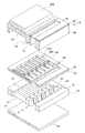
図1は、本発明の実施形態1に係る液体噴射ヘッドの一例であるインクジェット式記録ヘッドの概略構成を示す分解斜視図であり、図2は、図1の平面図及びそのA−A′断面図である。
Hereinafter, the present invention will be described in detail based on embodiments.
(Embodiment 1)
FIG. 1 is an exploded perspective view showing a schematic configuration of an ink jet recording head which is an example of a liquid ejecting head according to Embodiment 1 of the present invention. FIG. 2 is a plan view of FIG. FIG.
図示するように、流路形成基板10は、本実施形態では結晶面方位が(110)であるシリコン単結晶基板からなり、その一方面には予め熱酸化により形成した酸化シリコン(SiO2)からなる、厚さ0.5〜2.0μmの弾性膜50が形成されている。流路形成基板10には、複数の圧力発生室12がその幅方向に並設されている。また、流路形成基板10の圧力発生室12の長手方向外側の領域には連通部13が形成され、連通部13と各圧力発生室12とが、各圧力発生室12毎に設けられたインク供給路14及び連通路15を介して連通されている。連通部13は、後述する保護基板のリザーバ部31と連通して各圧力発生室12の共通のインク室となるリザーバの一部を構成する。インク供給路14は、圧力発生室12よりも狭い幅で形成されており、連通部13から圧力発生室12に流入するインクの流路抵抗を一定に保持している。なお、本実施形態では、流路の幅を片側から絞ることでインク供給路14を形成したが、流路の幅を両側から絞ることでインク供給路を形成してもよい。また、流路の幅を絞るのではなく、厚さ方向から絞ることでインク供給路を形成してもよい。さらに、各連通路15は、圧力発生室12の幅方向両側の隔壁11を連通部13側に延設してインク供給路14と連通部13との間の空間を区画することで形成されている。すなわち、流路形成基板10には、圧力発生室12の幅方向の断面積より小さい断面積を有するインク供給路14と、このインク供給路14に連通すると共にインク供給路14の幅方向の断面積よりも大きい断面積を有する連通路15とが複数の隔壁11により区画されて設けられている。
As shown in the figure, the flow
また、流路形成基板10の開口面側には、各圧力発生室12のインク供給路14とは反対側の端部近傍に連通するノズル開口21が穿設されたノズルプレート20が、接着剤や熱溶着フィルム等によって固着されている。なお、ノズルプレート20は、厚さが例えば、0.01〜1mmで、線膨張係数が300℃以下で、例えば2.5〜4.5[×10-6/℃]であるガラスセラミックス、シリコン単結晶基板又はステンレス鋼などからなる。
Further, on the opening surface side of the flow
一方、このような流路形成基板10の開口面とは反対側には、上述したように、厚さが例えば約1.0μmの弾性膜50が形成され、この弾性膜50上には、厚さが例えば、約0.4μmの絶縁体膜55が形成されている。さらに、この絶縁体膜55上には、厚さが例えば、約0.2μmの下電極膜60と、厚さが例えば、約1.1μmの圧電体層70と、厚さが例えば、約0.05μmの上電極膜80とが、後述するプロセスで積層形成されて、圧電素子300を構成している。ここで、圧電素子300は、下電極膜60、圧電体層70及び上電極膜80を含む部分をいう。一般的には、圧電素子300の何れか一方の電極を共通電極とし、他方の電極及び圧電体層70を各圧力発生室12毎にパターニングして構成する。そして、ここではパターニングされた何れか一方の電極及び圧電体層70から構成され、両電極への電圧の印加により圧電歪みが生じる部分を圧電体能動部320という。本実施形態では、下電極膜60は圧電素子300の共通電極とし、上電極膜80を圧電素子300の個別電極としているが、駆動回路や配線の都合でこれを逆にしても支障はない。何れの場合においても、各圧力発生室毎に圧電体能動部320が形成されていることになる。また、ここでは、圧電素子300と当該圧電素子300の駆動により変位が生じる振動板とを合わせてアクチュエータ装置と称する。なお、上述した例では、弾性膜50、絶縁体膜55及び下電極膜60が振動板として作用するが、弾性膜50、絶縁体膜55を設けずに、下電極膜60のみを残して下電極膜60を振動板としても良い。
On the other hand, as described above, the
ここで、本実施形態の下電極膜60は、要部概略断面を表す図3(a)に示すように、白金(Pt)層61と、その上の酸化チタン(TiOx)層62と、酸化イリジウム(IrOx)層63とを含むものである。また、白金層61は、柱状結晶からなり、各柱状結晶粒61aの粒界には、酸化チタン層62から連続して存在する酸化チタンからなる粒界層64を有するものである。
Here, the
これらの層は、後述するような製造プロセスで成膜後、圧電体前駆体膜を焼成して圧電体層70を形成する際に、熱拡散により形成されたものである。これらの層構造は顕微鏡観察により観察される結果を図示したものであり、明確に層構造を特定できない場合もあり、また、層の界面が明確でない場合もあるが、図3(a)に示される本実施形態の層構造は、後述する製造プロセスで形成されたものである。
These layers are formed by thermal diffusion when the
すなわち、本実施形態の下電極膜60は、製造プロセスを説明する後述する図4(c)に示すように、圧電体層70を形成する前に、絶縁体膜55上に設けられたチタンからなる密着層65と、密着層65上に設けられた白金層66と、白金層66上に設けられたイリジウムからなる拡散防止層67とを、順次形成した後、詳しくは後述する製造方法によって圧電体層70を焼成して結晶化させる際に同時に加熱処理されて形成されたものである。
That is, the
このような下電極膜60は、焼成において密着層65を構成するチタンが拡散して白金層61の柱状結晶粒61aの粒界に偏析して存在して粒界層64を有すると共に白金層61の上面に酸化チタン層62を有する。このように白金層61及びこれを形成する各柱状結晶粒61aが酸化チタンで囲まれているので、下電極膜60の剛性及び靱性が向上する。また、下電極膜60と酸化ジルコニウムからなる絶縁体膜55との密着性が良好になり、さらに、白金層61と酸化イリジウム層63とが酸化チタン層62を介して強固に密着されたものとなる。
Such a
なお、密着層65としては、本実施形態では、例えば、厚さが10〜50nmのチタン(Ti)を用いたが、例えば、クロム(Cr)、タンタル(Ta)、ジルコニウム(Zr)及びタングステン(W)からなる群から選択される少なくとも一つの元素を主成分とするものを密着層としてもよい。この場合には、チタンの代わりに他の金属が圧電体前駆体膜71の焼成時に拡散し、白金層61の柱状結晶粒61aの粒界及び白金層61の上面側には用いた他の金属の酸化物層が偏在することになる。
In this embodiment, for example, titanium (Ti) having a thickness of 10 to 50 nm is used as the
また、拡散防止層67としてイリジウム(Ir)を用いたが、パラジウム(Pb)、ロジウム(Rh)、ルテニウム(Ru)及びオスミウム(Os)からなる群から選択される少なくとも一つの元素を主成分とするものとしても同様な効果を奏することができる。なお、イリジウム以外の金属を用いた場合、下電極膜60の上部の酸化イリジウム層63は他の金属の酸化物からなる層となることはいうまでもない。
Further, although iridium (Ir) is used as the
また、圧電体層70は、下電極膜60上に形成される電気機械変換作用を示す強誘電性セラミックス材料からなるペロヴスカイト構造の結晶膜である。圧電体層70の材料としては、例えば、チタン酸ジルコン酸鉛(PZT)等の強誘電性圧電材料や、これに酸化ニオブ、酸化ニッケル又は酸化マグネシウム等の金属酸化物を添加したもの等が好適である。具体的には、チタン酸鉛(PbTiO3)、チタン酸ジルコン酸鉛(Pb(Zr,Ti)O3)、ジルコニウム酸鉛(PbZrO3)、チタン酸鉛ランタン((Pb,La),TiO3)ジルコン酸チタン酸鉛ランタン((Pb,La)(Zr,Ti)O3)又は、マグネシウムニオブ酸ジルコニウムチタン酸鉛(Pb(Zr,Ti)(Mg,Nb)O3)等を用いることができる。圧電体層70の厚さについては、製造工程でクラックが発生しない程度に厚さを抑え、且つ十分な変位特性を呈する程度に厚く形成する。例えば、本実施形態では、圧電体層70を1〜2μm前後の厚さで形成した。
The
さらに、圧電素子300の個別電極である各上電極膜80には、インク供給路14側の端部近傍から引き出され、絶縁体膜55上にまで延設される、例えば、金(Au)等からなるリード電極90が接続されている。
Further, each
このような圧電素子300が形成された流路形成基板10上、すなわち、下電極膜60、弾性膜50及びリード電極90上には、リザーバ100の少なくとも一部を構成するリザーバ部31を有する保護基板30が接着剤35を介して接合されている。このリザーバ部31は、本実施形態では、保護基板30を厚さ方向に貫通して圧力発生室12の幅方向に亘って形成されており、上述のように流路形成基板10の連通部13と連通されて各圧力発生室12の共通のインク室となるリザーバ100を構成している。
On the flow
また、保護基板30の圧電素子300に対向する領域には、圧電素子300の運動を阻害しない程度の空間を有する圧電素子保持部32が設けられている。圧電素子保持部32は、圧電素子300の運動を阻害しない程度の空間を有していればよく、当該空間は密封されていても、密封されていなくてもよい。
A piezoelectric
このような保護基板30としては、流路形成基板10の熱膨張率と略同一の材料、例えば、ガラス、セラミック材料等を用いることが好ましく、本実施形態では、流路形成基板10と同一材料のシリコン単結晶基板を用いて形成した。
As such a
また、保護基板30には、保護基板30を厚さ方向に貫通する貫通孔33が設けられている。そして、各圧電素子300から引き出されたリード電極90の端部近傍は、貫通孔33内に露出するように設けられている。
The
また、保護基板30上には、並設された圧電素子300を駆動するための駆動回路200が固定されている。この駆動回路200としては、例えば、回路基板や半導体集積回路(IC)等を用いることができる。そして、駆動回路200とリード電極90とは、ボンディングワイヤ等の導電性ワイヤからなる接続配線210を介して電気的に接続されている。
A
また、このような保護基板30上には、封止膜41及び固定板42とからなるコンプライアンス基板40が接合されている。ここで、封止膜41は、剛性が低く可撓性を有する材料(例えば、厚さが6μmのポリフェニレンサルファイド(PPS)フィルム)からなり、この封止膜41によってリザーバ部31の一方面が封止されている。また、固定板42は、金属等の硬質の材料(例えば、厚さが30μmのステンレス鋼(SUS)等)で形成される。この固定板42のリザーバ100に対向する領域は、厚さ方向に完全に除去された開口部43となっているため、リザーバ100の一方面は可撓性を有する封止膜41のみで封止されている。
In addition, a
このような本実施形態のインクジェット式記録ヘッドでは、図示しない外部インク供給手段と接続したインク導入口からインクを取り込み、リザーバ100からノズル開口21に至るまで内部をインクで満たした後、駆動回路200からの記録信号に従い、圧力発生室12に対応するそれぞれの下電極膜60と上電極膜80との間に電圧を印加し、弾性膜50、絶縁体膜55、下電極膜60及び圧電体層70をたわみ変形させることにより、各圧力発生室12内の圧力が高まりノズル開口21からインク滴が吐出する。
In such an ink jet recording head of this embodiment, ink is taken in from an ink introduction port connected to an external ink supply means (not shown), and the interior from the
以下、このようなインクジェット式記録ヘッドの製造方法について、図4〜図7を参照して説明する。なお、図4〜図7は、圧力発生室の長手方向の断面図である。まず、図4(a)に示すように、シリコンウェハである流路形成基板用ウェハ110を約1100℃の拡散炉で熱酸化し、その表面に弾性膜50を構成する二酸化シリコン(SiO2)からなる二酸化シリコン膜51を形成する。なお、本実施形態では、流路形成基板用ウェハ110として、膜厚が約625μmと比較的厚く剛性の高いシリコンウェハを用いている。
Hereinafter, a method for manufacturing such an ink jet recording head will be described with reference to FIGS. 4 to 7 are cross-sectional views in the longitudinal direction of the pressure generating chamber. First, as shown in FIG. 4A, a silicon wafer (SiO 2 ) that forms an
次いで、図4(b)に示すように、弾性膜50(二酸化シリコン膜51)上に、酸化ジルコニウムからなる絶縁体膜55を形成する。具体的には、弾性膜50(二酸化シリコン膜51)上に、例えば、スパッタ法等によりジルコニウム(Zr)層を形成後、このジルコニウム層を、例えば、500〜1200℃の拡散炉で熱酸化することにより酸化ジルコニウム(ZrO2)からなる絶縁体膜55を形成する。
Next, as shown in FIG. 4B, an
次いで、図4(c)に示すように、チタンからなる密着層65と、白金層66と、イリジウムからなる拡散防止層67とを順次積層した下電極膜60を形成する。具体的には、まず、絶縁体膜55上に、厚さ20nmのチタン(Ti)からなる密着層65を形成する。このように下電極膜60の最下層に密着層65を設けることによって、絶縁体膜55と下電極膜60との密着力を高めることができる。
Next, as shown in FIG. 4C, a
次いで、密着層65上に白金層66を形成する。白金層66は、例えば、スパッタリング法により成膜することができるが、スパッタリング法に限定されるものではなく、例えば、CVD法(化学蒸着法)等により形成するようにしてもよい。
Next, a
ここで、白金層66は、厚さ方向に結晶が伸びた柱状結晶とする必要があるが、結晶粒界に粒界層64を良好に形成するためには、白金層66を、できるだけきれいな柱状結晶とするのが好ましい。このようなきれいな柱状結晶の白金層66を形成するためには、例えば、スパッタリングの際の圧力を0.1Pa以下と低圧にする条件を採用するのが好ましい。また、さらに好ましくは、密着層65のスパッタリング条件を、例えば、0.1Pa以下と低圧とすることにより、白金層66の柱状結晶を良好にすることができることも実験で確認された。
Here, the
なお、このような柱状結晶の白金層66とすると、後述する圧電体層70の優先配向方位を、例えば、(100)とするために有効に作用する。
Note that such a columnar
このような下電極膜60は、詳しくは後述する圧電体層70を焼成により結晶化させる際に同時に加熱処理される。このとき、本実施形態では、密着層65上に白金層66及び拡散防止層67を設けたので、密着層65を構成する金属、すなわち、本実施形態でのチタン(Ti)は、拡散すると共に酸化されながら、図3に示すように、白金層61を形成する柱状結晶粒61aの粒界を通って、白金層61の上面側に進む。この際、酸化された酸化チタン(TiOx)が偏在した粒界層64を形成し、また、白金層61の上面側の酸化チタン層62を形成する。このような下電極膜60の最下層にある密着層65を、圧電体前駆体膜71を焼成して結晶化させる際の熱で拡散・酸化させて、酸化チタンなどの酸化物が白金層61の柱状結晶粒61aの粒界に偏析により存在、すなわち偏在させ易くなり、その結果下電極膜60の剛性、靱性を向上させることができ、繰り返し動作による劣化に対する耐性を向上させることができる。また、白金層61の粒界に密着性金属としての機能を奏する酸化チタン(TiOx)を偏在させることで、下電極膜60の上下の層が酸化チタンで繋がることになるので、下電極膜60の上下側の層との密着性を向上することができるという効果も奏する。
The
ここで、白金層61の柱状結晶粒61aの粒界に存在する粒界層64は、絶縁体膜55側にはできるだけ存在しないようにするのが好ましい。粒界層64が絶縁体膜55に近い柱状結晶粒61aの粒界に多く存在すると、白金層61の結晶方位の配向を乱し、白金層61が(111)に優先配向するのを阻害し、圧電体層70の成長を阻害する傾向があるからである。
Here, it is preferable that the
したがって、図3(b)に示すように、白金層61の柱状結晶粒61aの粒界の絶縁体膜55側には少なく存在し且つ圧電体層70側ほど多く存在するような粒界層64Aとするのが好ましい。ここで、粒界層64Aは、圧電体前駆体膜71を焼成して結晶化させる際の熱で密着層65が拡散・酸化され、酸化チタンなどの酸化物が白金層61の柱状結晶粒61aの粒界に偏析により形成されたものであるが、熱処理温度が高いほど密着層65の金属の拡散・酸化が生じ易いので、熱処理条件を高くするほど、絶縁体膜55側で少なく、圧電体層70側で多く存在する粒界層64Aが形成されやすい。
Therefore, as shown in FIG. 3B, the
次いで、粒界層64上に、拡散防止層67を形成する。これにより、密着層65、白金層66及び拡散防止層67からなる下電極膜60が形成される。なお、拡散防止層67は、後の工程で圧電体層70を焼成して結晶化させて形成する際に、密着層65及び白金層66の成分が圧電体層70に拡散するのを防止すると共に圧電体層70の成分が下電極膜60に拡散するのを防止するためのものである。このような拡散防止層67としては、本実施形態では厚さが5〜20nmのイリジウム(Ir)を用いたが、上述したように、パラジウム(Pb)、ロジウム(Rh)、ルテニウム(Ru)及びオスミウム(Os)からなる群から選択される少なくとも一つの元素を主成分とするものを用いてもよい。
Next, a
次いで、図4(d)に示すように、下電極膜60上にチタン(Ti)からなる種チタン層68を形成する。この種チタン層68は、3.5〜5.5nmの厚さで形成する。なお、種チタン層68の厚さは、4.0nmが好ましい。本実施形態では、種チタン層68を4.0nmの厚さで形成した。
Next, as shown in FIG. 4D, a
また、このように形成される種チタン層68は、その膜密度(Ti密度)ができるだけ高い方が好ましく、少なくとも4.5g/cm3以上であることが望ましい。種チタン層68の膜密度が高いほど時間経過に伴い表面に形成される酸化層の厚さは薄く抑えられ、圧電体層70の結晶が良好に成長するからである。なお、種チタン層68の膜密度は、厚さに関係なく成膜条件によって決まる。さらに、種チタン層68は非晶質であることが好ましい。具体的には、種チタン層68のX線回折強度、特に、(002)面のX線回折強度(XRD強度)が実質的に零となっていることが好ましい。このように種チタン層68が非晶質であると、種チタン層68の膜密度が高まり表層に形成される酸化層の厚みが薄く抑えられ、その結果、圧電体層70の結晶をさらに良好に成長させることができるからである。
The
このように下電極膜60の上に種チタン層68を設けることにより、後の工程で下電極膜60上に種チタン層68を介して圧電体層70を形成する際に、圧電体層70の優先配向方位を(100)または(111)に制御することができ、電気機械変換素子として好適な圧電体層70を得ることができる。なお、種チタン層68は、圧電体層70が結晶化する際に、結晶化を促進させるシードとして機能し、圧電体層70の焼成後には圧電体層70内に拡散するものである。
By providing the
なお、このような下電極膜60の各層65〜67及び種チタン層68は、例えば、DCマグネトロンスパッタリング法によって形成することができる。また、少なくとも下電極膜60の白金層66、拡散防止層67及び種チタン層68は、スパッタリング装置内の真空状態から開放せずに連続して成膜することが好ましい。このように下電極膜60の白金層66、拡散防止層67及び種チタン層68を連続成膜することによって、下電極膜60の白金層66、拡散防止層67及び種チタン層68の密着力を高めて下電極膜60内の層間剥離を防止することができる。
Note that each of the
次に、チタン酸ジルコン酸鉛(PZT)からなる圧電体層70を形成する。ここで、本実施形態では、金属有機物を触媒に溶解・分散したいわゆるゾルを塗布乾燥してゲル化し、さらに高温で焼成することで金属酸化物からなる圧電体層70を得る、いわゆるゾル−ゲル法を用いて圧電体層70を形成している。なお、圧電体層70の材料としては、チタン酸ジルコン酸鉛に限定されず、例えば、リラクサ強誘電体(例えば、PMN−PT、PZN-PT、PNN-PT等)の他の圧電材料を用いてもよい。また、圧電体層70の製造方法は、ゾル−ゲル法に限定されず、例えば、MOD(Metal-Organic Decomposition)法やスパッタリング法等を用いてもよい。つまり、高温をかけて熱処理して圧電体層70を形成する工程を有する成膜方法であることが好ましい。
Next, a
圧電体層70の具体的な形成手順としては、まず、図5(a)に示すように、下電極膜60上にPZT前駆体膜である圧電体前駆体膜71を成膜する。すなわち、下電極膜60が形成された流路形成基板10上に金属有機化合物を含むゾル(溶液)を塗布する(塗布工程)。次いで、この圧電体前駆体膜71を所定温度に加熱して一定時間乾燥させる(乾燥工程)。次に、乾燥した圧電体前駆体膜71を所定温度に加熱して一定時間保持することによって脱脂する(脱脂工程)。次に、図5(b)に示すように、圧電体前駆体膜71を所定温度に加熱して一定時間保持することによって結晶化させ、圧電体膜72を形成する(焼成工程)。
As a specific procedure for forming the
なお、このような乾燥工程、脱脂工程及び焼成工程で用いられる加熱装置としては、例えば、ホットプレートや、赤外線ランプの照射により加熱するRTP(Rapid Thermal Processing)装置などを用いることができる。 In addition, as a heating apparatus used in such a drying process, a degreasing process, and a baking process, for example, a hot plate, an RTP (Rapid Thermal Processing) apparatus that heats by irradiation with an infrared lamp, or the like can be used.
そして、図5(c)に示すように、下電極膜60上に圧電体膜72の1層目を形成した段階で、下電極膜60及び1層目の圧電体膜72をそれらの側面が傾斜するように同時にパターニングする。
5C, when the first layer of the
ここで、例えば、下電極膜60の上に種チタン層68を形成した後にパターニングしてから1層目の圧電体膜72を形成する場合、フォト工程・イオンミリング・アッシングして下電極膜60をパターニングするために種チタン層68が変質してしまい、変質した種チタン層68上に1層目の圧電体膜72を形成しても当該圧電体膜72の結晶性が良好なものではなくなり、1層目の圧電体膜72の上に形成される他の圧電体膜72も、1層目の圧電体膜72の結晶状態に影響して結晶成長するため、良好な結晶性を有する圧電体膜72が形成されない。
Here, for example, when forming the first
それに比べ、1層目の圧電体膜72を形成した後に下電極膜60と同時にパターニングすれば、1層目の圧電体膜72は種チタン層68に比べて2層目以降の圧電体膜72を良好に結晶成長させる種(シード)としても性質が強く、たとえパターニングで表層に極薄い変質層が形成されていても2層目以降の圧電体膜72の結晶成長に大きな影響を与えない。
In contrast, if the first
そして、パターニング後、上述した塗布工程、乾燥工程、脱脂工程及び焼成工程からなる圧電体膜形成工程を複数回繰り返すことで、図5(d)に示すように複数層の圧電体膜72からなる所定厚さの圧電体層70を形成する。例えば、ゾルの1回あたりの膜厚が0.1μm程度の場合には、例えば、10層の圧電体膜72からなる圧電体層70全体の膜厚は約1.1μm程度となる。
After the patterning, the piezoelectric film forming process including the coating process, the drying process, the degreasing process, and the baking process described above is repeated a plurality of times, thereby forming a plurality of
なお、上述のように下電極膜60上に圧電体膜72の1層目を形成した段階でこれらを同時にパターニングして、下電極膜60及び1層目の圧電体膜72の側面を傾斜させることで、2層目の圧電体膜72を形成する際に、下電極膜60及び1層目の圧電体膜72が形成された部分とそれ以外の部分との境界近傍において、下地の違いによる2層目の圧電体膜72の結晶性への悪影響を小さく、すなわち、緩和することができる。これにより、下電極膜60とそれ以外の部分との境界近傍において、2層目の圧電体膜72の結晶成長が良好に進み、結晶性に優れた圧電体層70を形成することができる。また、下電極膜60及び1層目の圧電体膜72の側面を傾斜させることで、2層目以降の圧電体膜72を形成する際の付き回りを向上することができる。これにより、密着性及び信頼性に優れた圧電体層70を形成することができる。
As described above, when the first layer of the
このように、圧電体層70を焼成して結晶化させる前の下電極膜60を、チタンからなる密着層65と白金層66とイリジウムからなる拡散防止層67とを構成し、圧電体前駆体膜71を焼成して圧電体層70を形成する際に上述した図3に示すような下電極膜60となるようにすることにより、下電極膜60の剛性、靱性を向上させることができ、繰り返し駆動による駆動耐久性を向上することができる。さらに、チタンからなる密着層65が拡散すると共に酸化して柱状結晶粒61aの粒界に粒界層64を形成すると共に酸化チタン層62が白金層61の上面側に存在することにより、下電極膜60と圧電体層70との密着性及び下電極膜60と流路形成基板用ウェハ110(絶縁体膜55)との密着性を向上することができる。
In this way, the
そして、図5(a)〜図5(d)に示す工程によって圧電体層70を形成した後は、図6(a)に示すように、例えば、イリジウム(Ir)からなる上電極膜80を流路形成基板用ウェハ110の全面に形成し、圧電体層70及び上電極膜80を、各圧力発生室12に対向する領域にパターニングして圧電素子300を形成する。
Then, after the
次に、リード電極90を形成する。具体的には、図6(b)に示すように、流路形成基板用ウェハ110の全面に亘って、例えば、金(Au)等からなるリード電極90を形成後、例えば、レジスト等からなるマスクパターン(図示なし)を介して各圧電素子300毎にパターニングすることで形成される。
Next, the
次に、図6(c)に示すように、流路形成基板用ウェハ110の圧電素子300側に、シリコンウェハであり複数の保護基板30となる保護基板用ウェハ130を接着剤35を介して接合する。なお、この保護基板用ウェハ130は、例えば、数百μm程度の厚さを有するため、保護基板用ウェハ130を接合することによって流路形成基板用ウェハ110の剛性は著しく向上することになる。そして、流路形成基板用ウェハ110をある程度の厚さとなるまで研磨した後、さらにフッ硝酸によってウェットエッチングすることにより流路形成基板用ウェハ110を所定の厚みにする。例えば、本実施形態では、数十μm厚になるように流路形成基板用ウェハ110をエッチング加工した。
Next, as shown in FIG. 6 (c), a
次いで、図7(a)に示すように、流路形成基板用ウェハ110上に、例えば、窒化シリコン(SiN)からなるマスク膜52を新たに形成し、所定形状にパターニングする。そして、図7(b)に示すように、流路形成基板用ウェハ110をマスク膜52を介してKOH等のアルカリ溶液を用いた異方性エッチング(ウェットエッチング)することにより、圧電素子300に対応する圧力発生室12、連通部13、インク供給路14及び連通路15等を形成する。
Next, as shown in FIG. 7A, a
その後は、流路形成基板用ウェハ110及び保護基板用ウェハ130の外周縁部の不要部分を、例えば、ダイシング等により切断することによって除去する。そして、流路形成基板用ウェハ110の保護基板用ウェハ130とは反対側の面にノズル開口21が穿設されたノズルプレート20を接合すると共に、保護基板用ウェハ130にコンプライアンス基板40を接合し、流路形成基板用ウェハ110等を図1に示すような一つのチップサイズの流路形成基板10等に分割することによって、本実施形態のインクジェット式記録ヘッドとする。
Thereafter, unnecessary portions of the outer peripheral edge portions of the flow path forming
なお、このようなインクジェット式記録ヘッドは、インクカートリッジ等と連通するインク流路を具備する記録ヘッドユニットの一部を構成して、インクジェット式記録装置に搭載される。図8は、そのインクジェット式記録装置の一例を示す概略図である。図8に示すように、インクジェット式記録ヘッドを有する記録ヘッドユニット1A及び1Bは、インク供給手段を構成するカートリッジ2A及び2Bが着脱可能に設けられ、この記録ヘッドユニット1A及び1Bを搭載したキャリッジ3は、装置本体4に取り付けられたキャリッジ軸5に軸方向移動自在に設けられている。この記録ヘッドユニット1A及び1Bは、例えば、それぞれブラックインク組成物及びカラーインク組成物を吐出するものとしている。 Such an ink jet recording head constitutes a part of a recording head unit including an ink flow path communicating with an ink cartridge or the like, and is mounted on the ink jet recording apparatus. FIG. 8 is a schematic view showing an example of the ink jet recording apparatus. As shown in FIG. 8, in the recording head units 1A and 1B having the ink jet recording head, cartridges 2A and 2B constituting ink supply means are detachably provided, and a carriage 3 on which the recording head units 1A and 1B are mounted. Is provided on a carriage shaft 5 attached to the apparatus body 4 so as to be movable in the axial direction. The recording head units 1A and 1B, for example, are configured to eject a black ink composition and a color ink composition, respectively.
そして、駆動モータ6の駆動力が図示しない複数の歯車およびタイミングベルト7を介してキャリッジ3に伝達されることで、記録ヘッドユニット1A及び1Bを搭載したキャリッジ3はキャリッジ軸5に沿って移動される。一方、装置本体4にはキャリッジ軸5に沿ってプラテン8が設けられており、図示しない給紙ローラなどにより給紙された紙等の記録媒体である記録シートSがプラテン8上を搬送されるようになっている。 The driving force of the driving motor 6 is transmitted to the carriage 3 via a plurality of gears and timing belt 7 (not shown), so that the carriage 3 on which the recording head units 1A and 1B are mounted is moved along the carriage shaft 5. The On the other hand, the apparatus body 4 is provided with a platen 8 along the carriage shaft 5, and a recording sheet S, which is a recording medium such as paper fed by a paper feed roller (not shown), is conveyed on the platen 8. It is like that.
以上、本発明の一実施形態について説明したが、本発明は、勿論、この実施形態に限定されるものではないことは言うまでもない。例えば、本実施形態では、液体噴射ヘッドの一例としてインクジェット式記録ヘッドを挙げて説明したが、本発明は広く液体噴射ヘッド全般を対象としたものであり、インク以外の液体を噴射する液体噴射ヘッドにも勿論適用することができる。その他の液体噴射ヘッドとしては、例えば、プリンタ等の画像記録装置に用いられる各種の記録ヘッド、液晶ディスプレー等のカラーフィルタの製造に用いられる色材噴射ヘッド、有機ELディスプレー、FED(電界放出ディスプレー)等の電極形成に用いられる電極材料噴射ヘッド、バイオchip製造に用いられる生体有機物噴射ヘッド等が挙げられる。また、本発明は、このような液体噴射ヘッドに圧力発生手段として搭載されるアクチュエータ装置だけでなく、あらゆる装置に搭載されるアクチュエータ装置に適用することができる。例えば、アクチュエータ装置は、上述したヘッドの他に、センサー等にも適用することができる。さらに、本発明は、液体噴射ヘッドに利用されるアクチュエータ装置としての圧電素子だけでなく、他のあらゆる装置、例えば、マイクロホン、発音体、各種振動子、発信子等に搭載される圧電素子にも適用できることは言うまでもない。 Although one embodiment of the present invention has been described above, it is needless to say that the present invention is not limited to this embodiment. For example, in the present embodiment, an ink jet recording head has been described as an example of a liquid ejecting head. However, the present invention is widely intended for all liquid ejecting heads, and ejects liquid other than ink. Of course, it can also be applied. Other liquid ejecting heads include, for example, various recording heads used in image recording apparatuses such as printers, color material ejecting heads used in the manufacture of color filters such as liquid crystal displays, organic EL displays, and FEDs (field emission displays). Examples thereof include an electrode material ejection head used for electrode formation, a bioorganic matter ejection head used for biochip production, and the like. The present invention can be applied not only to an actuator device mounted as pressure generating means on such a liquid jet head but also to an actuator device mounted on any device. For example, the actuator device can be applied to a sensor or the like in addition to the head described above. Furthermore, the present invention is not limited to a piezoelectric element as an actuator device used for a liquid ejecting head, but also to any other device, for example, a piezoelectric element mounted on a microphone, a sound generator, various vibrators, an oscillator, and the like. Needless to say, it can be applied.
10 流路形成基板、 12 圧力発生室、 13 連通部、 14 インク供給路、 20 ノズルプレート、 21 ノズル開口、 30 保護基板、 31 リザーバ部、 32 圧電素子保持部、 40 コンプライアンス基板、 60 下電極膜、 61 白金層、 62 酸化チタン層、 63 酸化イリジウム層、 64 粒界層、 65 密着層、 66 白金層、 67 拡散防止層、 68 種チタン層、 70 圧電体層、 80 上電極膜、 90 リード電極、 100 リザーバ、 200 駆動回路、 210 接続配線、 300 圧電素子
DESCRIPTION OF
Claims (5)
前記下電極膜は、前記圧電体層に向けて、柱状結晶を有する白金層と、酸化チタン層と、酸化イリジウム層と、を有し、
酸化チタンが前記白金層の結晶の粒界に存在していることを特徴とする圧電素子。 A piezoelectric element having a piezoelectric layer, and an upper electrode film and a lower electrode film configured to sandwich the piezoelectric layer,
The lower electrode film has a platinum layer having columnar crystals, a titanium oxide layer, and an iridium oxide layer toward the piezoelectric layer ,
The piezoelectric element characterized by titanium oxide is existed in the grain boundaries of crystals of the platinum layer.
Priority Applications (2)
| Application Number | Priority Date | Filing Date | Title |
|---|---|---|---|
| JP2007205320A JP5251031B2 (en) | 2006-09-08 | 2007-08-07 | Piezoelectric element, liquid ejecting head, liquid ejecting apparatus, sensor |
| US11/851,196 US7535157B2 (en) | 2006-09-08 | 2007-09-06 | Piezoelectric element, actuator device, liquid-jet head, and liquid-jet apparatus |
Applications Claiming Priority (3)
| Application Number | Priority Date | Filing Date | Title |
|---|---|---|---|
| JP2006243769 | 2006-09-08 | ||
| JP2006243769 | 2006-09-08 | ||
| JP2007205320A JP5251031B2 (en) | 2006-09-08 | 2007-08-07 | Piezoelectric element, liquid ejecting head, liquid ejecting apparatus, sensor |
Publications (3)
| Publication Number | Publication Date |
|---|---|
| JP2008091877A JP2008091877A (en) | 2008-04-17 |
| JP2008091877A5 JP2008091877A5 (en) | 2010-08-12 |
| JP5251031B2 true JP5251031B2 (en) | 2013-07-31 |
Family
ID=39169162
Family Applications (1)
| Application Number | Title | Priority Date | Filing Date |
|---|---|---|---|
| JP2007205320A Active JP5251031B2 (en) | 2006-09-08 | 2007-08-07 | Piezoelectric element, liquid ejecting head, liquid ejecting apparatus, sensor |
Country Status (2)
| Country | Link |
|---|---|
| US (1) | US7535157B2 (en) |
| JP (1) | JP5251031B2 (en) |
Families Citing this family (15)
| Publication number | Priority date | Publication date | Assignee | Title |
|---|---|---|---|---|
| JP5083496B2 (en) * | 2006-09-21 | 2012-11-28 | セイコーエプソン株式会社 | Actuator device, liquid jet head, and image recording apparatus |
| JP5320886B2 (en) | 2008-07-28 | 2013-10-23 | セイコーエプソン株式会社 | Liquid ejecting head, liquid ejecting apparatus, and piezoelectric element |
| US8164234B2 (en) * | 2009-02-26 | 2012-04-24 | Fujifilm Corporation | Sputtered piezoelectric material |
| JP2010201830A (en) * | 2009-03-04 | 2010-09-16 | Seiko Epson Corp | Liquid injection head, liquid injecting device, and piezoelectric element |
| JP5660274B2 (en) * | 2010-01-05 | 2015-01-28 | セイコーエプソン株式会社 | Liquid ejecting head manufacturing method, piezoelectric element manufacturing method, liquid ejecting head, liquid ejecting apparatus, and piezoelectric element |
| US9761785B2 (en) | 2011-10-17 | 2017-09-12 | The United States Of America As Represented By The Secretary Of The Army | Stylo-epitaxial piezoelectric and ferroelectric devices and method of manufacturing |
| US8866367B2 (en) | 2011-10-17 | 2014-10-21 | The United States Of America As Represented By The Secretary Of The Army | Thermally oxidized seed layers for the production of {001} textured electrodes and PZT devices and method of making |
| US20130320813A1 (en) | 2012-06-04 | 2013-12-05 | Tdk Corporation | Dielectric device |
| US8981627B2 (en) * | 2012-06-04 | 2015-03-17 | Tdk Corporation | Piezoelectric device with electrode films and electroconductive oxide film |
| JP2015079935A (en) * | 2013-09-11 | 2015-04-23 | 株式会社リコー | Piezoelectric actuator and droplet discharge head, and image forming apparatus |
| JP6263950B2 (en) * | 2013-10-22 | 2018-01-24 | 株式会社リコー | ELECTRO-MECHANICAL CONVERSION ELEMENT, MANUFACTURING METHOD THEREOF, DROPLET DISCHARGE HEAD HAVING ELECTRO-MECHANICAL CONVERSION ELEMENT, INK CARTRIDGE, AND IMAGE FORMING APPARATUS |
| KR102493684B1 (en) * | 2014-06-24 | 2023-01-31 | 울박, 인크 | Pzt thin film laminate and method for producing pzt thin film laminate |
| JP6460387B2 (en) * | 2015-01-26 | 2019-01-30 | Tdk株式会社 | Piezoelectric thin film element, piezoelectric actuator, piezoelectric sensor, hard disk drive, and inkjet printer apparatus |
| CN112864304A (en) * | 2019-11-12 | 2021-05-28 | 应用材料公司 | Fabrication of piezoelectric devices with PMNPT layers |
| US20240114800A1 (en) * | 2021-01-18 | 2024-04-04 | Applied Materials, Inc. | Deposition Of Piezoelectric Films |
Family Cites Families (15)
| Publication number | Priority date | Publication date | Assignee | Title |
|---|---|---|---|---|
| JP3890634B2 (en) * | 1995-09-19 | 2007-03-07 | セイコーエプソン株式会社 | Piezoelectric thin film element and ink jet recording head |
| JPH09129827A (en) | 1995-11-02 | 1997-05-16 | Sony Corp | Ferroelectric capacitor |
| JP4144043B2 (en) * | 1997-04-16 | 2008-09-03 | セイコーエプソン株式会社 | Method for manufacturing piezoelectric thin film element |
| JPH11151815A (en) | 1997-07-25 | 1999-06-08 | Seiko Epson Corp | Ink-jet type recording head and ink-jet type recording apparatus |
| JPH1197630A (en) * | 1997-09-22 | 1999-04-09 | Sharp Corp | Manufacture of ferroelectric thin film and ferroelectric memory device |
| JP3589560B2 (en) | 1998-01-27 | 2004-11-17 | 株式会社リコー | Ink jet head and method of manufacturing the same |
| DE69937713D1 (en) * | 1998-03-04 | 2008-01-24 | Seiko Epson Corp | PIEZOELECTRIC UNIT, INK JET PRINT HEAD, METHOD OF MANUFACTURE AND PRINTER |
| JPH11348277A (en) | 1998-06-04 | 1999-12-21 | Ricoh Co Ltd | Ink jet printer head |
| JP3685318B2 (en) * | 1999-11-09 | 2005-08-17 | セイコーエプソン株式会社 | Ferroelectric thin film element manufacturing method and heat treatment apparatus |
| JP2001223403A (en) * | 2000-02-08 | 2001-08-17 | Matsushita Electric Ind Co Ltd | Ferroelectric substance thin film, its forming method and ferroelectric substance thin film element using the thin film |
| JP3567977B2 (en) | 2000-03-24 | 2004-09-22 | セイコーエプソン株式会社 | Piezoelectric element, ink jet recording head, printer, and method of manufacturing piezoelectric element |
| US6534357B1 (en) * | 2000-11-09 | 2003-03-18 | Micron Technology, Inc. | Methods for forming conductive structures and structures regarding same |
| JP4029162B2 (en) | 2002-03-08 | 2008-01-09 | 株式会社村田製作所 | Method for manufacturing piezoelectric element |
| JP4208234B2 (en) | 2003-03-24 | 2009-01-14 | 株式会社ノリタケカンパニーリミテド | Conductive paste for piezoelectric ceramic material and use thereof |
| JP4761019B2 (en) * | 2004-10-04 | 2011-08-31 | セイコーエプソン株式会社 | Electrode film, piezoelectric element, ferroelectric capacitor, and semiconductor device |
-
2007
- 2007-08-07 JP JP2007205320A patent/JP5251031B2/en active Active
- 2007-09-06 US US11/851,196 patent/US7535157B2/en active Active
Also Published As
| Publication number | Publication date |
|---|---|
| US7535157B2 (en) | 2009-05-19 |
| JP2008091877A (en) | 2008-04-17 |
| US20080062228A1 (en) | 2008-03-13 |
Similar Documents
| Publication | Publication Date | Title |
|---|---|---|
| JP5251031B2 (en) | Piezoelectric element, liquid ejecting head, liquid ejecting apparatus, sensor | |
| JP4333686B2 (en) | Actuator device, liquid jet head, and liquid jet device | |
| JP4296441B2 (en) | Method for manufacturing actuator device | |
| JP2006245247A (en) | Piezoelectric element and its fabrication process, liquid ejection head and its manufacturing process, and liquid ejector | |
| JP2009113419A (en) | Manufacturing method of liquid jet head and manufacturing method of piezoelectric element | |
| JP2007073931A (en) | Actuator equipment, manufacturing method thereof, and liquid injection head and liquid injection equipment | |
| JP2006255972A (en) | Liquid jetting head, and liquid jetting device | |
| JP2011171335A (en) | Method of manufacturing piezoelectric actuator, piezoelectric actuator, liquid ejecting head and liquid ejecting device | |
| JP4811598B2 (en) | Actuator device, manufacturing method thereof, and liquid jet head | |
| JP5105040B2 (en) | Method for manufacturing piezoelectric element and method for manufacturing liquid jet head | |
| JP5257580B2 (en) | Liquid ejecting head, liquid ejecting apparatus, and piezoelectric element | |
| JP2007048816A (en) | Actuator apparatus, manufacturing method thereof, liquid injection head, and liquid injection apparatus | |
| JP5376107B2 (en) | Piezoelectric element and manufacturing method thereof, actuator device, liquid jet head, and liquid jet device | |
| JP5104609B2 (en) | Liquid ejecting head, liquid ejecting apparatus, and piezoelectric element | |
| JP5201304B2 (en) | Method for manufacturing actuator device and method for manufacturing liquid jet head | |
| JP2006245248A (en) | Piezoelectric element and its fabrication process, liquid ejection head and its manufacturing process, and liquid ejector | |
| JP2009226728A (en) | Manufacturing method of liquid jet head and manufacturing method of piezoelectric element | |
| JP2009076819A (en) | Actuator device, liquid jetting head and liquid jetting device | |
| JP2007173605A (en) | Method of manufacturing piezoelectric element and method of manufacturing liquid jetting head | |
| JP5365793B2 (en) | Method for manufacturing liquid jet head | |
| JP2007035883A (en) | Actuator device, its manufacturing method, and head and device for liquid injection | |
| JP2009208411A (en) | Method for manufacturing liquid injection head | |
| JP2008205048A (en) | Manufacturing method of piezoelectric element, and manufacturing method of liquid jetting head | |
| JP5716939B2 (en) | Liquid ejecting head, liquid ejecting apparatus, and actuator device | |
| JP2008066414A (en) | Method for manufacturing actuator apparatus and method for manufacturing liquid jet head |
Legal Events
| Date | Code | Title | Description |
|---|---|---|---|
| A521 | Request for written amendment filed |
Free format text: JAPANESE INTERMEDIATE CODE: A523 Effective date: 20100629 |
|
| A621 | Written request for application examination |
Free format text: JAPANESE INTERMEDIATE CODE: A621 Effective date: 20100629 |
|
| A131 | Notification of reasons for refusal |
Free format text: JAPANESE INTERMEDIATE CODE: A131 Effective date: 20121226 |
|
| A977 | Report on retrieval |
Free format text: JAPANESE INTERMEDIATE CODE: A971007 Effective date: 20121227 |
|
| A521 | Request for written amendment filed |
Free format text: JAPANESE INTERMEDIATE CODE: A523 Effective date: 20130222 |
|
| TRDD | Decision of grant or rejection written | ||
| A01 | Written decision to grant a patent or to grant a registration (utility model) |
Free format text: JAPANESE INTERMEDIATE CODE: A01 Effective date: 20130319 |
|
| A61 | First payment of annual fees (during grant procedure) |
Free format text: JAPANESE INTERMEDIATE CODE: A61 Effective date: 20130401 |
|
| R150 | Certificate of patent or registration of utility model |
Ref document number: 5251031 Country of ref document: JP Free format text: JAPANESE INTERMEDIATE CODE: R150 Free format text: JAPANESE INTERMEDIATE CODE: R150 |
|
| FPAY | Renewal fee payment (event date is renewal date of database) |
Free format text: PAYMENT UNTIL: 20160426 Year of fee payment: 3 |
|
| S531 | Written request for registration of change of domicile |
Free format text: JAPANESE INTERMEDIATE CODE: R313531 |
|
| R350 | Written notification of registration of transfer |
Free format text: JAPANESE INTERMEDIATE CODE: R350 |