JP5249483B2 - Semiconductor device and mask design method - Google Patents
Semiconductor device and mask design method Download PDFInfo
- Publication number
- JP5249483B2 JP5249483B2 JP2001506596A JP2001506596A JP5249483B2 JP 5249483 B2 JP5249483 B2 JP 5249483B2 JP 2001506596 A JP2001506596 A JP 2001506596A JP 2001506596 A JP2001506596 A JP 2001506596A JP 5249483 B2 JP5249483 B2 JP 5249483B2
- Authority
- JP
- Japan
- Prior art keywords
- feature
- polishing
- features
- polishing dummy
- layer
- Prior art date
- Legal status (The legal status is an assumption and is not a legal conclusion. Google has not performed a legal analysis and makes no representation as to the accuracy of the status listed.)
- Expired - Lifetime
Links
Images


Classifications
-
- H—ELECTRICITY
- H01—ELECTRIC ELEMENTS
- H01L—SEMICONDUCTOR DEVICES NOT COVERED BY CLASS H10
- H01L21/00—Processes or apparatus adapted for the manufacture or treatment of semiconductor or solid state devices or of parts thereof
- H01L21/02—Manufacture or treatment of semiconductor devices or of parts thereof
- H01L21/027—Making masks on semiconductor bodies for further photolithographic processing not provided for in group H01L21/18 or H01L21/34
-
- H—ELECTRICITY
- H01—ELECTRIC ELEMENTS
- H01L—SEMICONDUCTOR DEVICES NOT COVERED BY CLASS H10
- H01L21/00—Processes or apparatus adapted for the manufacture or treatment of semiconductor or solid state devices or of parts thereof
- H01L21/02—Manufacture or treatment of semiconductor devices or of parts thereof
- H01L21/04—Manufacture or treatment of semiconductor devices or of parts thereof the devices having at least one potential-jump barrier or surface barrier, e.g. PN junction, depletion layer or carrier concentration layer
- H01L21/18—Manufacture or treatment of semiconductor devices or of parts thereof the devices having at least one potential-jump barrier or surface barrier, e.g. PN junction, depletion layer or carrier concentration layer the devices having semiconductor bodies comprising elements of Group IV of the Periodic System or AIIIBV compounds with or without impurities, e.g. doping materials
- H01L21/30—Treatment of semiconductor bodies using processes or apparatus not provided for in groups H01L21/20 - H01L21/26
- H01L21/31—Treatment of semiconductor bodies using processes or apparatus not provided for in groups H01L21/20 - H01L21/26 to form insulating layers thereon, e.g. for masking or by using photolithographic techniques; After treatment of these layers; Selection of materials for these layers
- H01L21/3105—After-treatment
- H01L21/31051—Planarisation of the insulating layers
- H01L21/31053—Planarisation of the insulating layers involving a dielectric removal step
-
- H—ELECTRICITY
- H01—ELECTRIC ELEMENTS
- H01L—SEMICONDUCTOR DEVICES NOT COVERED BY CLASS H10
- H01L21/00—Processes or apparatus adapted for the manufacture or treatment of semiconductor or solid state devices or of parts thereof
- H01L21/02—Manufacture or treatment of semiconductor devices or of parts thereof
- H01L21/04—Manufacture or treatment of semiconductor devices or of parts thereof the devices having at least one potential-jump barrier or surface barrier, e.g. PN junction, depletion layer or carrier concentration layer
- H01L21/18—Manufacture or treatment of semiconductor devices or of parts thereof the devices having at least one potential-jump barrier or surface barrier, e.g. PN junction, depletion layer or carrier concentration layer the devices having semiconductor bodies comprising elements of Group IV of the Periodic System or AIIIBV compounds with or without impurities, e.g. doping materials
- H01L21/30—Treatment of semiconductor bodies using processes or apparatus not provided for in groups H01L21/20 - H01L21/26
- H01L21/31—Treatment of semiconductor bodies using processes or apparatus not provided for in groups H01L21/20 - H01L21/26 to form insulating layers thereon, e.g. for masking or by using photolithographic techniques; After treatment of these layers; Selection of materials for these layers
- H01L21/3205—Deposition of non-insulating-, e.g. conductive- or resistive-, layers on insulating layers; After-treatment of these layers
- H01L21/321—After treatment
- H01L21/32115—Planarisation
- H01L21/3212—Planarisation by chemical mechanical polishing [CMP]
-
- Y—GENERAL TAGGING OF NEW TECHNOLOGICAL DEVELOPMENTS; GENERAL TAGGING OF CROSS-SECTIONAL TECHNOLOGIES SPANNING OVER SEVERAL SECTIONS OF THE IPC; TECHNICAL SUBJECTS COVERED BY FORMER USPC CROSS-REFERENCE ART COLLECTIONS [XRACs] AND DIGESTS
- Y10—TECHNICAL SUBJECTS COVERED BY FORMER USPC
- Y10S—TECHNICAL SUBJECTS COVERED BY FORMER USPC CROSS-REFERENCE ART COLLECTIONS [XRACs] AND DIGESTS
- Y10S438/00—Semiconductor device manufacturing: process
- Y10S438/926—Dummy metallization
Description
(本発明の技術分野)
本発明は、半導体デバイス及びマスク一般、より詳細には、ダミーフィーチャを有する半導体デバイス及びマスクに関する。(Technical field of the present invention)
The present invention relates generally to semiconductor devices and masks, and more particularly to semiconductor devices and masks having dummy features.
(関連する技術)
半導体デバイスの形成において、表面を平坦化するために研磨が使用される。従来は、半導体デバイスの形成においてタイリングは使用されていなかった。タイリングが使用されない場合には、研磨は、陥没、或いは半導体デバイス基板にわたる厚さの不均一性に関する他の問題を生じていた。これらの問題には、リソグラフィの焦点深度の超過、或いは図1に示されるようなエッチングに関する問題が含まれる。図1は、導電層11を含む基板を示す。絶縁層12が形成され、導電層11まで延びる開口を有するようにパターニングされる。導電性の充填材料(例えばタングステン等)が開口内部に堆積され、導電プラグ13を形成すべく、研磨される。導電プラグが近接した間隔を有する場合に研磨は、より多くの絶縁層12を磨滅することがある。その後、導電プラグ13を被覆して絶縁層16が形成される。絶縁層16の上面は平坦である。(Related technology)
In the formation of semiconductor devices, polishing is used to planarize the surface. Traditionally, tiling has not been used in the formation of semiconductor devices. When tiling was not used, polishing had caused depressions or other problems with thickness non-uniformity across the semiconductor device substrate. These problems include exceeding the depth of focus of lithography, or problems with etching as shown in FIG. FIG. 1 shows a substrate including a conductive layer 11. An
次に、開口17が形成される。いくつかの箇所においては、磨滅のために開口が導電プラグ13まで完全に延びていないため、図1に示されるように、開口17とその下方の導電プラグ13との間に絶縁間隙19を残す。電気的な開放が形成される。間隙19を除去するためにエッチングが続けられる場合、既に露出された伝導プラグ13はオーバーエッチングされ、典型的には高い接触抵抗に帰着する。従って、部分的には研磨によって生じた厚さの不均一性は、電気的な開放、高抵抗の接触、電気の短絡、或いは他の漏れ電流の経路に帰着することがある。 Next, the opening 17 is formed. In some places, the opening does not extend completely to the
陥没、及びその他の厚さにより累積された効果に関する問題を解決する試みとしてダミーフィーチャが使用されてきた。研磨を補助するために使用されるダミーフィーチャは、ダミーフィーチャのパターンを半導体の上方から観察するとタイルのように視認されることに因んだ、「タイリング」により形成される。タイリングのためのプロセスは典型的に、回路レイアウトの形成、レイアウト内のアクティブフィーチャの周辺におけるバッファ領域(典型的には約5〜10ミクロンの範囲内)の画定、及び、空地を決定するために回路レイアウトに最小領域を組み合わせることを含む。他の全ての領域はタイリングに利用可能である。 Dummy features have been used in an attempt to solve problems related to depression and other effects accumulated by thickness. The dummy features used to assist polishing are formed by “tiling” due to the fact that the pattern of dummy features is viewed like a tile when viewed from above the semiconductor. The process for tiling is typically to form a circuit layout, define buffer areas around active features in the layout (typically in the range of about 5-10 microns), and determine open space And combining the minimum area with the circuit layout. All other areas are available for tiling.
タイリングは、アクティブフィーチャのうちのいずれかの間の距離が、最小幅以上である場合に、回路密度に依存せずに使用される。典型的には、最小幅は10ミクロン未満であり、約10ミクロンであることも可能である。タイル、或いは少なくともタイルの一部は、少なくとも5ミクロンの幅を有して利用可能な領域に設けられる。タイリングパターン(即ち、タイルのサイズ及び密度)は通常、半導体デバイス全体にわたり、同一である。米国特許第5,278,105号及びヨーロッパ特許出願公開第0712 156号(1996)号のそれぞれの図5を参照する。タイルの一部は欠けているが、同一のフィーチャ密度が使用される。 Tiling is used independent of circuit density when the distance between any of the active features is greater than or equal to the minimum width. Typically, the minimum width is less than 10 microns and can be about 10 microns. The tile, or at least a portion of the tile, is provided in an available area having a width of at least 5 microns. The tiling pattern (ie, tile size and density) is usually the same throughout the semiconductor device. Reference is made to FIG. 5 of US Pat. No. 5,278,105 and European Patent Application No. 0712 156 (1996), respectively. Some of the tiles are missing but the same feature density is used.
本発明は、例示の目的において、かつ限定するものではなく、添付された図面に示される。図面において、同一の符号は同一の構成要素を示す。
当業者は、図面の構成要素が、単純化及び明確化のために示されるものであり、必ずしも一定の比率に拡大して示されていないことを認識する。例えば、本発明の実施形態に対する理解の向上を促進するために、図面の構成要素のうちのいくつかの寸法が他の要素よりも誇張されていてもよい。The present invention is illustrated by way of example and not limitation, in the accompanying drawings. In the drawings, the same reference numeral indicates the same component.
Those skilled in the art will recognize that the components in the drawings are shown for simplicity and clarity and have not necessarily been shown to scale. For example, some dimensions of the components of the drawings may be exaggerated over other elements to facilitate improved understanding of the embodiments of the present invention.
(詳細な説明)
研磨ダミーフィーチャをどこに配置すべきか決定する際には、物理的近接効果、電気的近接効果、或いは両方が考慮される。研磨ダミーフィーチャは、半導体デバイスの性能に恵影響を及ぼすことなく十分に平坦性を達成すべく、1つ以上のフィーチャ層に、挿入され、除去され、移動され、或いは変更されることが可能である。即ち、研磨ダミーフィーチャパターンの幾分無差別な配置ではなく、研磨ダミーフィーチャパターンのより選択的配置が使用される。トポグラフィ変化の低周波数(数百ミクロン以上)及び高周波数(10ミクロン以下)の両方が検討された。本発明の実施形態はその最大限に実施された場合には、信号の完全性を保持しつつ、十分な平坦性を可能とする。本発明は請求項に規定され、詳細な説明を読むことによって、一層理解される。(Detailed explanation)
In determining where to place the polishing dummy feature, physical proximity effects, electrical proximity effects, or both are considered. Polishing dummy features can be inserted, removed, moved, or modified in one or more feature layers to achieve sufficient flatness without adversely affecting the performance of the semiconductor device. is there. That is, rather than a somewhat indiscriminate arrangement of polishing dummy feature patterns, a more selective arrangement of polishing dummy feature patterns is used. Both low frequencies (over a few hundred microns) and high frequencies (below 10 microns) of topographic changes were considered. Embodiments of the present invention, when implemented to its fullest extent, allow for sufficient flatness while maintaining signal integrity. The invention is defined in the claims and will be better understood by reading the detailed description.
明細書の理解を補助すべく、いくつかの用語が以下に定義される。
1.アクティブフィーチャとは、半導体デバイスのために設計された回路に相当するフィーチャである。アクティブフィーチャには、トランジスタ、キャパシタ、レジスタ等の部分が含まれる。アクティブフィーチャには、ほぼ一定の電位で作動するように設計された電力供給フィーチャ、及びある電子条件においては1つの電位で、他の電子条件においては異なる電位で作動するように設計された信号フィーチャが含まれる。To assist in understanding the specification, a number of terms are defined below.
1. An active feature is a feature corresponding to a circuit designed for a semiconductor device. Active features include parts such as transistors, capacitors, resistors, and the like. Active features include power supply features that are designed to operate at a substantially constant potential, and signal features that are designed to operate at one potential in some electronic conditions and at a different potential in other electronic conditions. Is included.
2.制御フィーチャとは、基板の加工処理の制御を補助するフィーチャである。制御フィーチャには、アラインメントマーク、フィーチャの寸法を測定するための構造体(「CDバー」)、電気テスト構造体等が含まれる。制御フィーチャは典型的には、半導体デバイス基板上のダイス間にあるスクライブライン内に設けられる。 2. The control feature is a feature that assists in controlling the processing of the substrate. Control features include alignment marks, structures for measuring feature dimensions ("CD bars"), electrical test structures, and the like. The control features are typically provided in scribe lines between dies on the semiconductor device substrate.
3.環境保護フィーチャとは、形成後の環境条件から半導体デバイスを保護する主要な(最重要の)機能を有するフィーチャである。ダイスの周辺のエッジリングシールが、環境保護デバイスの最も一般的、かつほぼ唯一の例である。エッジリングシールは、ダイシング、及びパッケージの処理の間に可動性イオンからの防護を提供する。 3. An environmental protection feature is a feature that has a primary (most important) function of protecting a semiconductor device from environmental conditions after formation. An edge ring seal around the die is the most common and almost only example of an environmental protection device. The edge ring seal provides protection from mobile ions during dicing and package processing.
4.集積回路領域とは、アクティブフィーチャを備えたダイスの部分である。典型的には、集積回路領域は、ダイス端部の近傍のボンドパッドによって区画される。 4). An integrated circuit area is a portion of a die with active features. Typically, the integrated circuit area is bounded by bond pads near the die edge.
5.周辺領域とは、ダイスの、集積回路領域とスクライブラインとの間に位置する部分である。多くの集積回路では、周辺領域は、ダイスのボンドパッドとスクライブラインとの間にある部分である。 5. The peripheral region is a portion of the die located between the integrated circuit region and the scribe line. In many integrated circuits, the peripheral region is the portion between the die bond pad and the scribe line.
6.解像度補助フィーチャとは、半導体デバイス基板上に印刷されるべき、アクティブフィーチャの解像度を改良させる、解像度補充フィーチャである。解像度補助フィーチャはマスクにはあるが、基板上に対する個別のフィーチャとしてはプリントされない。移相シフタが解像度補助フィーチャの例である。本明細書の目的において、光学的接近効果の補正のために加えられたフィーチャは、解像度補助フィーチャと考えられる。 6). A resolution assist feature is a resolution fill feature that improves the resolution of active features to be printed on a semiconductor device substrate. Resolution assist features are present in the mask but are not printed as individual features on the substrate. A phase shift shifter is an example of a resolution assist feature. For purposes herein, features added for correction of optical proximity effects are considered resolution assist features.
7.ダミーフィーチャには、半導体デバイス基板上にプリントされたフィーチャであって、上記に定義された他の種類のフィーチャのいずれでもないフィーチャが含まれる。様々な理由により、異なる種類のダミーフィーチャが半導体デバイスに使用される。アレイ中の全てのアクティブビットラインを均一にパターニングすることを可能とするために、メモリアレイの最も外側の端部に沿って、ダミービットラインが使用される。ダミービットラインと異なり、研磨ダミーフィーチャは、この層、或いは次に形成される層における研磨特性を改善するために半導体デバイスのマスクのフィーチャ層に加えられたダミーフィーチャである。研磨ダミーフィーチャは、デバイスの適切な作動には必要ではない。 7). Dummy features include features printed on a semiconductor device substrate that are not any of the other types of features defined above. Different types of dummy features are used in semiconductor devices for various reasons. Dummy bit lines are used along the outermost edges of the memory array to allow uniform patterning of all active bit lines in the array. Unlike dummy bit lines, a polishing dummy feature is a dummy feature added to a feature layer of a mask of a semiconductor device to improve the polishing characteristics in this layer, or a subsequently formed layer. The polishing dummy feature is not necessary for proper operation of the device.
8.電子デザインルールとは、間隔の最小値、フィーチャのサイズ、或いは集積回路内のフィーチャ間のオーバラップについての規則である。電子デザインルールは、部分的にはマージン及びデバイス特性(ラッチアップに対する免疫、リーク電流等)の処理により決定される。 8). Electronic design rules are rules for minimum spacing, feature size, or overlap between features in an integrated circuit. Electronic design rules are determined in part by processing margins and device characteristics (immunity to latch-up, leak current, etc.).
9.研磨ダミーフィーチャデザインルールとは、電子デザインルールの部分集合であるが、研磨ダミーフィーチャに特有のものである。従来から、研磨ダミーフィーチャとアクティブフィーチャとの間、或いは他の研磨ダミーフィーチャとの最小の間隔は、少なくとも5ミクロンであり、典型的には約10ミクロン以下である。 9. Polishing dummy feature design rules are a subset of electronic design rules, but are specific to polishing dummy features. Traditionally, the minimum spacing between polishing dummy features and active features, or other polishing dummy features, is at least 5 microns, typically less than about 10 microns.
10.空地領域差とは、同一のフィーチャ層における、研磨ダミーフィーチャとアクティブフィーチャとの間の最小間隔と、2つのアクティブフィーチャ間の最小間隔との差である。 10. The air space area difference is a difference between the minimum distance between the polishing dummy feature and the active feature and the minimum distance between the two active features in the same feature layer.
本明細書に開示された発明の理解の簡便性を補助するために、限定するものではない特定の例が記載される。例は、まず単一のフィーチャ層に注目し、次に、多数のフィーチャ層の集積化に注目する。厚さ約0.8ミクロンの金属含有層からコンダクタのパターンが形成される。約1.5ミクロンの酸化物層が次に、コンダクタのパターンを覆って形成され、研磨される。議論の焦点は、コンダクタのパターン形成、及び、減少された起伏を有して研磨された酸化物層の形成を補助するための研磨ダミーフィーチャに向けられる。 In order to assist in the understanding of the invention disclosed herein, specific examples, which are not limiting, are described. The example first focuses on a single feature layer and then focuses on the integration of multiple feature layers. A conductor pattern is formed from a metal-containing layer about 0.8 microns thick. An approximately 1.5 micron oxide layer is then formed over the conductor pattern and polished. The focus of the discussion is on polishing dummy features to assist in patterning the conductor and forming an oxide layer that has been polished with reduced relief.
図2は、レイアウトにおいて、どこに研磨ダミーフィーチャが設けられるべきかを決定するためのプロセスを示すプロセスフローチャート10である。このプロセスはレイアウト(ブロック102)の生成により開始する(ブロック100)。レイアウトはこの時点において、典型的にはアクティブフィーチャ、及び制御フィーチャを有する。研磨ダミーフィーチャは有していない。その後、レイアウトは、レイアウトを調整すべく、随意に処理される。最小の幾何学的形状のフィーチャは、プリント、或いはエッチングのバイアスを補償すべく、サイズ変更されてもよい。解像度補助フィーチャも典型的には加えられる。この特定の実施形態においては、研磨ダミーフィーチャは、この時点においてレイアウトにない。しかし、研磨ダミーフィーチャは他の実施形態においてはあることが可能である。 FIG. 2 is a
ブロック104においては、トポグラフィ表記が行われるか否かが決定される。行われない場合には、酸化物研磨プロセスはブロック112によりキャラクタリゼーションされ、ブロック114において相互作用距離が決定される。このキャラクタリゼーションは、テストウェハを使用して実行されることが可能である。図3は、基板20及び層22の上面図である。形成されるべきコンダクタの厚さが約0.8ミクロンであるため、層22も厚さが約0.8ミクロンである必要がある。典型的には、基板20及び層22に使用された材料は重要ではない。層22は、導電層を使用する代わりに、約0.8ミクロンの厚さの絶縁層であることが可能である。しかし、完成したデバイスにおいて比較的により圧縮力を有する層(例えば、低いkを有した有機誘電材料)が導体の下にある場合には、より正確に研磨プロセスの特性値を決定するために、基板20は、同一の、又は類似した材料を使用する必要がある可能性もある。 In
層22は形成された後、回路レイアウトの一部であるコンダクタ端部に類似した端部を擬態すべく、パターニングされる。ウェハの半分は図3においてパターニングされるが、他のパターン、例えばチェッカーボード、ストライプを使用することが可能である。その後、研磨されるべき層がパターニングされた表面上に形成される。層の材料及び厚さは、半導体デバイス上で研磨されるべき層とほぼ同一である必要がある。この特定の例においては、層は二酸化ケイ素を含み、約1.5ミクロンの厚さを有する。研磨されるべき層が複数の異なる膜からなるか、ドーパントを有する場合には、テストウェハ用の層も異なる膜、或いはドーパントを含む必要がある。 After
次に、層32が図4に示されるように研磨される。テストウェハのための研磨条件は、半導体デバイス基板用の研磨条件と可能な限り厳密に一致している必要がある。研磨特性に影響を及ぼすことがある研磨パラメタには、研磨パッドの堅さ(1つ以上の材料の硬度及び厚さ)、下向きの圧力、研磨流体の組成、圧盤回転速度等が含まれる。 Next, the
研磨後の層32の厚さは、両面において、層22の端部から離隔した箇所(約50〜100ミリメートル(mm))では比較的に一定である。層32の高さが変化する箇所には、移行距離34がある。研磨特性である移行距離34は、典型的には少なくとも約0.3mmであり、多くの場合において約1.0mmである。層間絶縁層、或いはトレンチフィールドアイソレーションのために研磨されるいくつかの酸化物については、移行距離34は、約5〜10mmの範囲内であることが可能である。研磨するパラメタを変更する場合の移行距離34の感度は未知である。しかし、完成品の基板上の移行距離が約50%異なる場合であっても、テストウェハの移行幅は、研磨ダミーフィーチャの配置を決定する際に使用可能である。 The thickness of the
相互作用距離は、プロセスの使用者により決定されるが、典型的には、移行距離の少なくとも半分である。アクティブフィーチャから相互作用距離内に設けられた研磨ダミーフィーチャは、研磨及び平坦化に対してより少ない影響を及ぼしている。例えば、移行距離は約6mmである。相互作用距離は、約3mmである。タイリングが使用される場合には、研磨ダミーフィーチャ(タイル)は、少なくとも回路レイアウト部では、最も近接したアクティブフィーチャ(例えば、ゲート電極、ビットライン、接続等)から約3mmよりも近接している必要がない。典型的には、フィーチャ層においてアクティブフィーチャの最大密度を有する、マスク又はデバイスの領域は、研磨ダミーフィーチャを最も必要としない。従って、研磨ダミーフィーチャは、最も密度が高いアクティブフィーチャパターン内の最も近接したアクティブフィーチャから約3mmおいて、次の層の研磨に著しく影響を与えることなく、設けられていてもよい。 The interaction distance is determined by the user of the process, but is typically at least half of the transition distance. A polishing dummy feature provided within an interaction distance from the active feature has less impact on polishing and planarization. For example, the transition distance is about 6 mm. The interaction distance is about 3 mm. If tiling is used, the polishing dummy feature (tile) is closer than about 3 mm from the closest active feature (eg, gate electrode, bit line, connection, etc.), at least in the circuit layout section. There is no need. Typically, the area of the mask or device that has the highest density of active features in the feature layer requires the least number of polishing dummy features. Accordingly, polishing dummy features may be provided approximately 3 mm from the closest active feature in the densest active feature pattern without significantly affecting polishing of the next layer.
このことを、アクティブフィーチャの密度が通常考慮されない従来のタイリング方法と比較する。これらの従来の方法においては、空地が、最高密度にあるアクティブフィーチャに近接するか、或いは最低密度にあるアクティブフィーチャに近接するかと関係なく、その幅が少なくとも5〜10ミクロンであり、長さが少なくとも5〜10ミクロンである空地に、タイルが配置される。従って、従来の方法は、最も近接したアクティブフィーチャ或いは他のダミーフィーチャから10ミクロン以下に設けられている研磨ダミーフィーチャパターン端部の研磨ダミーフィーチャを典型的に有する。ここで、相互作用距離は、従来の空地のタイリングのために使用された最小の横方向の寸法よりも、3桁弱だけ高い。本発明の実施形態は、少なくとも約50ミクロンの幅及び長さを備えた空地を有することが可能である。 This is compared with conventional tiling methods where the density of active features is not normally considered. In these conventional methods, the width is at least 5-10 microns, regardless of whether the open space is adjacent to the highest density active feature or the lowest density active feature, and the length is Tiles are placed in open areas that are at least 5-10 microns. Thus, conventional methods typically have polishing dummy features at the edge of the polishing dummy feature pattern that are no more than 10 microns from the closest active feature or other dummy feature. Here, the interaction distance is a little less than three orders of magnitude higher than the minimum lateral dimension used for conventional open space tiling. Embodiments of the invention can have open areas with a width and length of at least about 50 microns.
相互作用距離情報を使用すると、研磨ダミーフィーチャは、回路レイアウト(ブロック132)内に設けることが可能である。この時点においては典型的に、その後の気相成長及び研磨の後に生じる表面が十分に平坦か否かを決定すべく検証(ブロック134)が行われる。平坦であれば、プロセスは終了する。そうでなければ、この時点においてアクティブフィーチャ、及び研磨ダミーフィーチャを含んでいる、レイアウト内の研磨ダミーフィーチャパターンが修正される。予測された平坦性が許容可能となるまで、プロセスを反復することが可能である。 Using the interaction distance information, polishing dummy features can be provided in the circuit layout (block 132). At this point, verification (block 134) is typically performed to determine whether the surface resulting after subsequent vapor deposition and polishing is sufficiently flat. If flat, the process ends. Otherwise, the polishing dummy feature pattern in the layout, including the active features and polishing dummy features at this point, is modified. The process can be repeated until the predicted flatness is acceptable.
上記したプロセスと併せて、或いは代替手段として、他のプロセスを使用可能である。再び図2を参照すると、トポグラフィ表記を使用可能である(ブロック104)。この例においては、研磨プロセスの特性値が決定されない(「NO」の経路に沿ったブロック118)ことが予想される。図5は、2つのメモリアレイ42,44、及びロジック領域46を有する半導体デバイス40のレイアウトの図である。アレイ42,44、及びロジック領域46のそれぞれは、少なくとも50ミクロンかける50ミクロンであり、多くの場合において、少なくとも500ミクロンかける500ミクロンである。アレイ及び領域は任意の形状であることが可能であり、正方形又は直線的形状に限定されない。表記は事実上全てのアクティブフィーチャを有する(事実上全てのゲート電極、ワードライン、ビットライン、接続、等を示す)ことが予想されるが、簡単に理解されるために、レイアウトのブロックダイアグラムが使用される。この例において、メモリアレイ42,44は、スタティックランダムアクセスメモリ(SRAM)アレイであり、ロジック領域46は、中央処理装置、算術論理演算ユニット、これらの組み合わせ等を含む。多種(ダイナミックランダムアクセスメモリ(DRAM)アレイ、フローティングゲートメモリアレイ、強誘電体ランダムアクセスメモリ(FERAM)アレイ等)のメモリアレイを使用してもよい。さらに、メモリアレイ42,44は異なる種類のメモリアレイであることもある。本明細書において使用されるように、メモリアレイの領域はメモリアレイの最も外側のメモリセル端部により画定され、列、又はカラムデコーダ、感度増幅器等を含んでいない。 Other processes can be used in conjunction with or as an alternative to the processes described above. Referring again to FIG. 2, topographic notation can be used (block 104). In this example, it is expected that the characteristic value of the polishing process is not determined (block 118 along the “NO” path). FIG. 5 is a layout diagram of a
図5を参照する。メモリアレイ42,44、及びロジック領域46は、典型的には互いに約10〜100ミクロンの範囲内にある。図示されていないが、メモリアレイ42,44は、同一のメモリアレイ内の他のメモリブロックから少なくとも10ミクロン離隔しているメモリブロック(サブアレイ)を有することが可能である。メモリアレイ42,44は高密度回路(近接して離隔されたポリサイドワードライン、金属ワードライン及びビットライン)を有する。ロジック領域46は局部的な高密度回路領域を有するが、その全面的な回路密度は、メモリアレイ42,44の回路密度より著しく低い。 Please refer to FIG.
図2のブロック122を再び参照する。空間的、或いは周波数ドメインにおいて第1のトポグラフィ表記がなされることが可能である。空間的ドメインにおいては、表記は、等高線地図に類似しているが、平均値と比較した相対的な高さの差を示す。この種の表現を生成することが可能であるプログラムは、カリフォルニア州フリーモントのアバント社により製造されているヘラクレス階層的設計検証ソフトウェア(ヘラクレス階層的デザインルールチェックソフトウェアとしても公知)である。ここでも、実際の表現は、図5に示されたものよりはるかに詳細にわたる。フーリエ変換機能を使用して、空間の表現を周波数ドメインに変換すること、及びその逆が可能である。 Reference is again made to block 122 of FIG. A first topographic representation can be made in the spatial or frequency domain. In the spatial domain, the notation is similar to a contour map, but shows the relative height difference compared to the mean value. A program that can generate this type of representation is Hercules hierarchical design verification software (also known as Hercules hierarchical design rule checking software) manufactured by Avant, Fremont, California. Again, the actual representation is much more detailed than that shown in FIG. Using the Fourier transform function, it is possible to convert the representation of space to the frequency domain and vice versa.
図2のブロック124においては、その後、図6の第2のトポグラフィ表記を形成すべく、第1のトポグラフィ表記の焦点が外され、或いはぼかされる。最高点は、メモリアレイ42,44の間の点である位置52であり、最低点は、ロジック領域の端部の外側、或いは近傍の領域であるポイント54である。 In
焦点を外すこと、即ちぼかすことは、多様な方法で行うことが可能である。焦点を外す単純な方法は、詳細なトポグラフィの色を付けた空間的地図を得て、目の焦点をぼかすことである。より低い解像度を達成する他の方法は、第1の表現の透明なシートを形成し、オーバーヘッドプロジェクタにそれを置くことである。より高いポイント及び低いポイントがどこにあるかを一般的に決定すべく、画像の焦点を確実に外す。第2のトポグラフィ表記を得る他の方法は、第1のトポグラフィ表記の周波数ドメインを使用し、低いパスフィルタによって加工することである。低いパスフィルタは微視的な変化(トポグラフィにおける高周波数の変化)を無視するが、巨視的な変化(トポグラフィにおける低周波数の変化)を維持する。周波数ドメイン表現が空間的ドメインに変換される場合、第2の表現は、図6のように視認される。図6は、焦点を外した後の空間的地図を示す。ポイント52は最高点を示し、ポイント54は最低点を示す。 Defocusing can be done in a variety of ways. A simple way to defocus is to get a spatial map with detailed topographic colors and blur the eye. Another way to achieve lower resolution is to form a transparent sheet of the first representation and place it on an overhead projector. Ensure that the image is defocused to generally determine where the higher and lower points are. Another way to obtain the second topography notation is to use the frequency domain of the first topography notation and process with a low pass filter. A low pass filter ignores microscopic changes (high frequency changes in topography), but maintains macroscopic changes (low frequency changes in topography). If the frequency domain representation is converted to the spatial domain, the second representation is viewed as in FIG. FIG. 6 shows the spatial map after defocusing.
次に、図7に示されるような、図2の随意のブロック126に示されるように、相補的イメージが形成される。相補的イメージは、本質的に図6に示されるものの逆である。図7の相補的イメージは、研磨ダミーフィーチャが最も必要であるポイント64、及び研磨ダミーフィーチャが最も必要としない、或いは回避されるべきポイント62を含む。相補的イメージは、空間的、或いは周波数ドメインにより表現されることが可能である第3のトポグラフィ表記である。 Next, a complementary image is formed, as shown in
この時点では、研磨ダミーフィーチャは回路レイアウト(図2のブロック132)に設けられることが可能であり、生じたレイアウトが、その後の堆積及び研磨後に十分に平坦であるか否かを決定すべく検証される。平坦であれば、プロセスは終了する。 At this point, a polishing dummy feature can be provided in the circuit layout (block 132 of FIG. 2) and verified to determine whether the resulting layout is sufficiently flat after subsequent deposition and polishing. Is done. If flat, the process ends.
平坦でなければ、この時点においてアクティブフィーチャ、及び研磨ダミーフィーチャを含んでいる、レイアウト内の研磨ダミーフィーチャパターンが修正される。修正は、研磨ダミーフィーチャの追加、又は除去、或いはこれらの密度若しくは形状を変更することが可能である。 If not flat, the polishing dummy feature pattern in the layout, including the active features and polishing dummy features at this point, is modified. The modifications can add or remove polishing dummy features, or change their density or shape.
プロセスは、予測された平坦性が許容可能となるまで反復可能である。反復においては、異なる位置まで遡ることが可能である。図2の決定ブロック142を参照する。最短の繰り返しループでは、研磨ダミーフィーチャの配置(ブロック132)に遡る。決定ブロック144では、レイアウトがこの時点においてアクティブフィーチャ、及び研磨ダミーフィーチャを含んでいるブロック102に、反復を戻すことが可能である。代替手段として、アクティブ及び研磨ダミーフィーチャを含むレイアウトの焦点をずらすことが可能である(ブロック124)。 The process can be repeated until the predicted flatness is acceptable. Iterations can be traced back to different positions. Refer to decision block 142 of FIG. The shortest iteration loop goes back to the polishing dummy feature placement (block 132). At
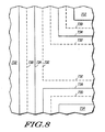
研磨ダミーフィーチャの挿入、及び位置の調節が図8に示される。図8に示されるような検査された領域(ウィンドウ)の量は、上記された研磨特性のうちの1つである相互作用距離と関係がある必要がある。検査された領域が相互作用距離と比較して、小さい場合には、最適の研磨ダミーフィーチャパターンが達成されていない可能性がある。他の形状よりも円形或いは長方形(正方形を含む)が使用されることが多いが、ウィンドウは、事実上任意の形状であることが可能である。ウィンドウは、通常は少なくとも相互作用距離のほぼ10分の1、或いは少なくとも約0.3mmの、幅(直径、或いは平面上の2つの方向のうちでより小さい方)を有する。多くの場合において、ウィンドウは、相互作用距離の約0.3〜3.0倍の範囲内、又は約1.0〜10.0mmの範囲内に、直径(円形)、又はそれぞれの幅及び長さ(直線形)を有する。ウィンドウがレチクルフィールド全体よりも小さい場合、レチクルフィールド全体を含めるようにウィンドウが拡大される、さらなる検査が行なわれる必要がある。 The insertion of the polishing dummy feature and the adjustment of the position are shown in FIG. The amount of inspected area (window) as shown in FIG. 8 needs to be related to the interaction distance, which is one of the polishing characteristics described above. If the inspected area is small compared to the interaction distance, the optimal polishing dummy feature pattern may not be achieved. Although a circle or rectangle (including squares) is often used rather than other shapes, the window can be of virtually any shape. The window has a width (diameter or the smaller of the two directions on the plane), usually at least approximately one-tenth of the interaction distance, or at least about 0.3 mm. In many cases, the window has a diameter (circular) within the range of about 0.3 to 3.0 times the interaction distance, or within the range of about 1.0 to 10.0 mm, or the width and length of each. (Straight). If the window is smaller than the entire reticle field, further inspection needs to be done in which the window is enlarged to include the entire reticle field.
アクティブフィーチャ710,712,714がレイアウトに設けられる。第1のパスでは、研磨ダミーフィーチャは、電子デザインルールにより除外される以外は全ての位置に加えられる。この特定の実施形態においては、個々の研磨ダミーフィーチャは、アクティブフィーチャから少なくとも5ミクロン離間している必要がある。研磨ダミーフィーチャは図8において、このフィーチャ層のアクティブフィーチャ710,712,714の間に加えられている。元来の研磨の形状は、破線730により示されている。この研磨ダミーフィーチャがトポグラフィのシミュレーションに挿入される場合、焦点を外した表現は、続けて形成される層の上面の高さが、図8に示される基板の部分としては高すぎることを示す。
研磨ダミーフィーチャのサイズは、破線732により示される形状に縮小される。この研磨ダミーフィーチャの形状が、破線730に対応する形状を置き換える。ここで、形状730のうちアクティブフィーチャ710及び714の間に位置する部分は除去されている。この形状が許容される場合には使用可能である。縮みが必要な調節を過補償した場合には、形状734が生じる可能性がある。形状734の一部はアクティブフィーチャ710,714の間を延伸する。しかし、形状734が形状732を拡大したバージョンである場合には、その部分は必要でなくてもよい。 The size of the polishing dummy feature is reduced to the shape indicated by the dashed
代替のプロセスとして、研磨キャラクタリゼーション(ブロック112,114)、及びトポグラフィ表記の両方を実行することが可能である(ブロック122,124,126)。回路レイアウト(ブロック132)に研磨ダミーフィーチャを設ける場合には、両方のパスからの情報を使用することが可能である。例えばトポグラフィ表記は、例えばタイルのような研磨ダミーフィーチャが配置されるべき位置を決定するために使用可能である。研磨キャラクタリゼーションは、アクティブフィーチャと最も近接している研磨ダミーフィーチャとの間の最小距離を決定するために使用可能である。1つの実施形態において研磨キャラクタリゼーションは1回行われるが、トポグラフィ表記及び研磨ダミーフィーチャの配置は任意の回数反復することが可能である。研磨ダミーフィーチャの配置が適切であることを確認した後、マスクを生成することが可能である。 As an alternative process, both polishing characterization (
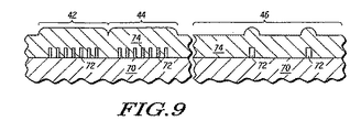
図9は、メモリアレイ42,44、並びにロジック領域46(図5を参照)が形成されている半導体デバイス基板70の一部を示す。この例において、基板70は絶縁層を含み、基板70上に導体72が形成される。メモリアレイ42,44内において、導体72はトランジスタ(図示せず)のドレイン領域との電気的接触を形成するビットラインである。ロジック領域46内では導体は、多様な部品(トランジスタ、コンデンサ、レジスタ等)に電気的に接続された接続である。図9は、上に重ねられた絶縁層74がどのようにして絶縁層74の上部の表面に沿って様々な形状を有するか(研磨ダミーフィーチャは加えられていない)を示す。研磨ダミーフィーチャが加えられず、基板が絶縁層74を平坦化するために研磨される場合、メモリアレイ42,44中の基板70上の絶縁層74の厚さはロジック領域46の基板70上の絶縁層74の厚さより厚い。従来のタイリング法は、5〜10ミクロンの範囲内の幅を有する空地に研磨ダミーフィーチャ(図示せず)を設ける。そのような位置の1つはメモリアレイ42,44の間にある。 FIG. 9 shows a part of the
本発明の実施形態に従い、研磨ダミーフィーチャ82はコンダクタ72と同一のフィーチャ層においてマスクに挿入される。生じるパターンは、図10の半導体デバイスに見られる。ここで、メモリアレイ42,44の間のギャップ84には研磨ダミーフィーチャが設けられていない。間隙は、約20〜100ミクロンの範囲の幅にある。さらに、類似の間隙(図示せず)が、メモリアレイ42,44の少なくとも一方のメモリブロックの間に設けられていてもよい。 In accordance with an embodiment of the present invention, the polishing
典型的には、研磨ダミーフィーチャ82は最も高いアクティブフィーチャ密度を有する領域内で最も近接した導体72(アクティブフィーチャ)から少なくとも約0.3mm、多くの場合には少なくとも1mm離れている。この特定の実施形態において、最も高いアクティブフィーチャ密度を有する領域内においてアクティブフィーチャに最も近い研磨ダミーフィーチャ82は、互いに約3〜5mmの範囲内だけ離隔して設けられている(研磨ダミーフィーチャからアクティブフィーチャへの間隔)。ここでも、この値は現在当業者が使用している(10ミクロンより大きな空地の全てに無差別なタイルを配置する)よりも約3桁高い。研磨ダミーフィーチャのための最小間隙及び間隔は上記の研磨キャラクタリゼーシヨンにより少なくとも部分的に決定された。 Typically, the polishing
基板70上にコンダクタ72及び研磨ダミーフィーチャ82が形成された後、導体72及び研磨ダミーフィーチャ82上に1つ以上の絶縁体の膜を堆積することにより絶縁層74が形成される。 After the
図10の左側(アレイ42,44)のための絶縁層74上部表面の平均的高さは、ロジック領域46上の絶縁層74の上面の平均的高さに近い。 The average height of the top surface of the insulating
層74を堆積した後、次に図11に示されるようなほぼ平坦な表面92を達成すべく研磨される。研磨に使用される条件は、上記されたキャラクタリゼーションにおいて使用される条件に類似している必要がある。従って、研磨パッドに類似するもの、類似の研磨流体、及び類似の研磨パラメタは、少なくとも研磨ダミーフィーチャの配置を部分的に決定したこれらのパラメタが研磨キャラクタリゼーションに影響するため、使用される必要がある。研磨の結果、完全に平坦な表面が生じる必要はない。起伏の程度は、それが電子的性能(電気的短絡やリークパスがない)、或いは後の工程(リソグラフィ又はエッチングに関連した問題における焦点深度)に著しく影響しないことが必要である。 After depositing
他の多数の実施形態が可能である。図12は、SRAMアレイ44がDRAMアレイ121に置換された場合におけるデバイス40の拡大図である。DRAMアレイ121はトレンチ容量、及び埋め込みのビットライン(ビットラインは半導体デバイス基板内に設けられる)を有する。図12に示される箇所は、SRAMアレイ42、DRAMアレイ121、及びロジック領域46の境界の近傍である。アレイ及び領域の境界が図12に示されているが、これらの境界は参考のためのものであり、設計され、或いは形成される、マスクや半導体デバイスには現れない。この実施形態において、導体の1段は、SRAMアレイ42上に高密度にあり、ロジック領域46上に準高密度にあり(Vssパワーバス1251及びVDDパワーバス1271)、DRAMアレイ121上に存在しないか、非常に低密度にあるアクティブフィーチャ(SRAMアレイ42用のビットライン123)を有する。Many other embodiments are possible. FIG. 12 is an enlarged view of the
研磨ダミーフィーチャ129,1253,1255,1273,1275がレイアウトに挿入される。アレイ42は図12に示される研磨ダミーフィーチャを有しない。例えばアレイ42のように最も高いアクティブフィーチャ密度を有する半導体デバイスの部分は、研磨ダミーフィーチャを有する。代替手段として、研磨ダミーフィーチャに利用可能な領域(アクティブフィーチャの外側の領域であり、電子デザインルールのための最小の間隔)については、最も高いアクティブフィーチャ密度を有するこれらの部分は、より低いアクティブフィーチャ密度領域と比較して、研磨ダミーフィーチャによって占領されている領域がより小さくてもよい。 Polishing dummy features 129, 1253, 1255, 1273, 1275 are inserted into the layout. The
本明細書にて使用される、ある領域におけるフィーチャ密度とは、いかなるフィーチャにも占領されていない状態でのその領域の全面積に対する、任意の種類のフィーチャにて被覆された領域のパーセンテージである。換言すると、フィーチャ密度は、フィーチャが占領する領域の面積をその領域の合計の面積で割ったパーセンテージである。メモリアレイ121のフィーチャ密度は、全てのメモリアレイが研磨ダミーフィーチャ129により被覆されるため、最も高い。ロジック領域46のフィーチャ密度は、本実施形態においては、あらゆる研磨ダミーフィーチャを有しないにも関わらず最低である。メモリアレイ42のフィーチャ密度は、メモリアレイ42,121フィーチャ密度の間にある。ここで、フィーチャ密度は、半導体デバイスの3つの異なる領域の任意の2つについて同一ではない。 As used herein, feature density in a region is the percentage of the region covered by any type of feature relative to the total area of that region when not occupied by any feature. . In other words, feature density is the percentage of the area occupied by a feature divided by the total area of that area. The feature density of
図12の研磨ダミーフィーチャに関していくつかの項目が特筆される。研磨ダミーフィーチャは典型的には、電気的にフローティングにした状態にされているか、或いは電源に接続される。この実施形態において研磨ダミーフィーチャ129,1253,1255は、Vss電源ターミナルにカップリング、或いは電気接続されており、研磨ダミーフィーチャ1273,1275はVDD電源ターミナルにカップリング、或いは電気接続される。研磨ダミーフィーチャ129は配列121用のα粒子や放射線効果の影響を弱めることを補助する接地された平面であってもよい。研磨ダミーフィーチャ1253,1255、並びにVssパワーバス1251の一部は、1組のデカップリングコンデンサであり、研磨ダミーフィーチャ1273,1275、並びにVDDパワーバス1271の一部は、異なる1組のデカップリングコンデンサである。他の回路(図示せず)からの負荷やシグナルがVssパワーバス1251上、或いはVDDパワーバス1271の電位に変化を生じさせる場合には、デカップリングコンデンサ(フィーチャ1253,1255、又はフィーチャ1273,1275)の他の電極が、電位降下の減少、又はパワーバスがその適正なポテンシャルに近づくために要する時間を減少させることを補助する。ここで、バスと、その最も近傍にある研磨フィーチャとの間の間隔は、フィーチャ(マスキング)層において最も接近しているアクティブフィーチャ間で使用される間隔よりも小さくてもよい。例えば、電子デザインルールは、アクティブフィーチャ間に約0.5ミクロンの最小間隔を必要としてもよい。しかし、間隔のリソグラフィ限界は0.2ミクロンである可能性がある。研磨ダミーフィーチャとそれらに対応するパワーバスとの間の間隔は、容量のカップリングを増加させるためには、約0.2〜0.4ミクロンの範囲内である可能性がある。Several items are noted with respect to the polishing dummy feature of FIG. The polishing dummy feature is typically left electrically floating or connected to a power source. In this embodiment, polishing dummy features 129, 1253, and 1255 are coupled or electrically connected to a Vss power supply terminal, and polishing dummy features 1273 and 1275 are coupled or electrically connected to a V DD power supply terminal. The polishing
研磨ダミーフィーチャ129及びビットライン123は、距離1297だけ離隔しており、研磨ダミーフィーチャ1255及びビットライン123のうちの1つは、距離1257だけ離隔している。それぞれの距離1297,1257は、フィーチャ129,1255のそれぞれと、ビットライン123との間の最近接箇所を示す。ここで、これらの間隔にはいかなるアクティブフィーチャ、或いは研磨ダミーフィーチャが設けられていない。距離1297は約0.3mmであることがあり、距離1257は約1.0mmであることがある。他の実施形態においてこれらの距離は、これよりも大きく、或いは小さくなることが可能である。 The polishing
研磨による層の過度の摩耗は、典型的にはスクライブライン近傍の半導体デバイスの端部近傍に見られる。図13は、半導体デバイス基板139の一部の上面図である。基板は集積回路領域(図示されていないメモリアレイ及びロジック領域)を有した4つの半導体デバイス40からなる。図13は、半導体デバイス40間のスクライブライン内にある制御フィーチャ、例えば、寸法測定ダガー1331、アライメントマーク1333、及び電気テスト構造(N+レジスタ)1335を示す。他の制御フィーチャ(図示せず)は、スクライブラインに沿った他のいずれかの箇所、或いは半導体デバイス40と共に配置されてもよい。研磨ダミーフィーチャ135は、半導体デバイス40の端部近傍の局部的高研磨速度の悪影響を緩和するためにスクライブラインに加えられる。本実施形態において研磨ダミーフィーチャ135は、図10の導体72及び研磨ダミーフィーチャ82と同一の層に形成され、半導体デバイス基板に重ねられてもよい。後で記載するように、半導体デバイスの周辺領域内に研磨ダミーフィーチャを追加することは、摩耗の量を減少させることも促進する。Excessive wear of the layer due to polishing is typically found near the edge of the semiconductor device near the scribe line. FIG. 13 is a top view of a part of the
さらなる他の実施形態において研磨ダミーフィーチャは他の層に配置することが可能である。例えば、研磨ダミーフィーチャ配置は、トレンチフィールドアイソレーションの工程中に形成された半導体(シリコン、シリコンゲルマニウム等)のメサの配置に影響を及ぼすことがある。メサのパターンは、続いて堆積され、研磨されるトレンチ充填材料(酸化物、窒化物、シリコン等)の研磨キャラクタリゼーションから少なくとも部分的に決定することが可能である。上記のプロセスは、導電体の、即ち金属含有層を堆積し、研磨する前に形成される絶縁層のパターンにも適用可能である。 In still other embodiments, the polishing dummy features can be placed on other layers. For example, polishing dummy feature placement may affect the placement of semiconductor (silicon, silicon germanium, etc.) mesas formed during the trench field isolation process. The mesa pattern can be determined at least in part from the polishing characterization of the trench fill material (oxide, nitride, silicon, etc.) that is subsequently deposited and polished. The above process is also applicable to the pattern of the insulating layer formed prior to depositing and polishing the conductor, i.e. the metal-containing layer.
研磨ダミーフィーチャは、研磨が使用される全ての層にある必要はない。省略された研磨ダミーフィーチャの影響は層が多くなることに伴い蓄積する。研磨ダミーフィーチャはいくつかの層のみに加えられてもよい。1つの実施形態において半導体デバイス40内のSRAMアレイ42,44は、上記されたDRAMアレイ121に類似したDRAMアレイにより置き換えられてもよい。この場合も半導体デバイスはロジック領域46を有する。接続の第1の層には、DRAMアレイについては金属ワードラインを形成し、ロジック領域46には比較的より少数の接続を形成してもよい。接続の第2の層にはあったとしても非常に少数の接続をDRAMアレイに形成し(埋め込まれたビットラインを有するため)、ロジック領域46には比較的多数の接続を形成してもよい。第2の接続の層が形成され、絶縁層によって被覆された後、絶縁層の上面は、比較的互いに近接しているDRAMアレイ、及びロジック領域46上わたり、平均的高さを有する(これら2つの領域間において100ナノメートル未満の差)。 The polishing dummy feature need not be in every layer where polishing is used. The effect of omitted polishing dummy features accumulates with more layers. Polishing dummy features may be added to only some layers. In one embodiment, the
接続の第3の層がバス、パワーレール等(Vss,VDD)を含んで形成される。第3の層の接続の密度は、ロジック領域46に比較してDRAMアレイの方がより高くてもよい。本実施形態において研磨ダミーフィーチャは、接続の第1及び第2の層には使用されず、接続の第3の層にのみ加えられる。A third layer of connections is formed including buses, power rails, etc. (V ss , V DD ). The connection density of the third layer may be higher in the DRAM array than in the
アクティブフィーチャ及び研磨ダミーフィーチャの間の増加した間隔は、2つの種類のフィーチャ間の寄生容量カップリングを減少させる。この減少された寄生容量カップリングは、より少ない悪影響をもって非常に高周波で半導体デバイスを駆動させることを可能にする。 The increased spacing between the active feature and the polishing dummy feature reduces the parasitic capacitance coupling between the two types of features. This reduced parasitic capacitance coupling makes it possible to drive semiconductor devices at very high frequencies with fewer adverse effects.
いくつかの実施形態において研磨ダミーフィーチャは、他の研磨ダミーフィーチャに接触していてもよい。図14において、フィールドアイソレーション領域1412は、半導体デバイス基板1410の一部の上部に形成される。ゲート絶縁層1416及びゲート電極1418は、基板1410の主要な表面上にある。基板1410内にドープされた領域1414が形成される。トランジスタ構造及びフィールドアイソレーション領域1412上に第1の絶縁層1432が形成される。ドープされた領域1414のうちの1つに伝導プラグ1434が形成される。第1の絶縁層1432上に接続1451が形成される。研磨ダミーフィーチャ1453も、接続1451と同一のフィーチャ層に形成される。 In some embodiments, the polishing dummy feature may be in contact with other polishing dummy features. In FIG. 14, the
第2の絶縁層1455が、接続1451及び研磨ダミーフィーチャ1453上に形成される。伝導プラグ1457,1459が形成される。本実施形態において伝導プラグ1457はデバイスとして設計された電気回路の一部であるため、アクティブフィーチャである。伝導プラグ1459は研磨ダミーフィーチャである。ここで、伝導プラグ1459は研磨ダミーフィーチャ1453に接触している。その後、伝導プラグ1457,1459上に、接続1471及び研磨ダミーフィーチャ1473が形成される。研磨ダミーフィーチャ1473は、これもまた研磨ダミーフィーチャである伝導プラグ1459に接触する。ほぼ完成した半導体デバイスを形成すべくパッシベーション層が形成される。 A second insulating
研磨プロセスは、研磨ダミーフィーチャを挿入する必要性を減少させて研磨特性を改善するべく、変更することが可能である。より堅いパッド、より少ない下向きの圧力、及びより高い圧盤回転速度は、移行距離、及び相互作用距離を増加させる可能性がある。相互作用距離が半導体デバイス、レチクルフィールド、或いは、さらには基板よりも大きい場合には、研磨ダミーフィーチャが全く必要ではない可能性がある。 The polishing process can be modified to improve the polishing characteristics by reducing the need to insert polishing dummy features. Stiffer pads, less downward pressure, and higher platen rotation speed can increase the transition distance and interaction distance. If the interaction distance is greater than the semiconductor device, reticle field, or even the substrate, no polishing dummy feature may be required.
上記の概念は多層においても拡張可能である。図15,16に見られるように、研磨ダミーフィーチャの配置は、他の層にあるアクティブフィーチャの電気特性に影響することがある。図15を参照すると、導体152,154,156は、半導体デバイス内において、それぞれVss,VDD,VPPを供給するアクティブフィーチャである。層151,158,159は絶縁体である。より下側にあるフィーチャ層が、導体152,154,156の下側の領域内に研磨ダミーフィーチャを必要とする。研磨ダミーフィーチャ153,155,157は、導体152,154,156の下方に加えられる。研磨ダミーフィーチャ153,155,157は、研磨ダミーフィーチャと電力供給コンダクタの間の容量カップリングを増加させるべく導電性を有し、それぞれVss,VDD,VPP電力供給ターミナルに電気接続されている。このことは、導体152,154,156上に負荷が配置される場合に、電位の振動を減少させることを補助する。ここで、導体152,154,156の側方の端部は、研磨ダミーフィーチャ153,155,157の側方の端部と境界線を共にする。導体152,154,156がほぼ同一の電位にある場合には、単一の研磨ダミーフィーチャ(図示せず)が研磨ダミーフィーチャ152,154,156を置換してもよい。単一の研磨ダミーフィーチャの端部は、導体152の左側端部及び導体156の右側端部と境界線を共にしていてもよい。The above concept can be extended in multiple layers. As seen in FIGS. 15 and 16, the placement of the polishing dummy features may affect the electrical characteristics of active features in other layers. Referring to FIG. 15,
図示されていないが、内部に設けられており、或いは設けられていないこともあるフィールドアイソレーション領域の一部である半導体メサは同一の概念である。研磨ダミーフィーチャは、基板内のノイズに対する容量、或いは基板内にウェル領域を形成するためにメサ上に設けられることが可能である。メサがp型半導体材料を含んでいる場合、この上にある研磨ダミーフィーチャは典型的にはVssターミナルにカップリングされ、又は電気的に接続される。n型半導体材料については、その上にある研磨ダミーフィーチャは、典型的にはVDDターミナルにカップリングされ、或いは電気的に接続される。電力供給コンダクタと同様に、容量のカップリングは高い値に保持される必要がある。この特定の場合において研磨ダミーフィーチャは、隣接する層のフィーチャの下方にあるのではなく、上方にある。Although not shown, a semiconductor mesa that is a part of a field isolation region that is provided inside or may not be provided is the same concept. The polishing dummy feature can be provided on the mesa to form a capacitance to noise in the substrate, or a well region in the substrate. If the mesa includes a p-type semiconductor material, the overlying dummy dummy feature is typically coupled or electrically connected to a V ss terminal. For n-type semiconductor material, the polishing dummy feature on it is typically coupled to or electrically connected to a V DD terminal. As with the power supply conductor, the capacitive coupling needs to be kept high. In this particular case, the polishing dummy feature is above rather than below the features of the adjacent layer.
電力供給コンダクタと異なり、信号コンダクタに対する容量カップリングは、最小限にするか、或いは少なくとも減少されている必要がある。図16は、アクティブフィーチャである信号コンダクタ162,164,166を示す。層161,168,169は絶縁体である。研磨ダミーフィーチャ163,165は導電性を有し、より低いフィーチャ層に加えられている。ここで、研磨ダミーフィーチャ163,165は、信号コンダクタ162,164,166からオフセットになっており、信号フィーチャの間に位置する絶縁層169の一部の下方にある。オフセットは、これがない場合にはコンダクタ162,164,166に沿って送信される信号の速度、又は完全性(強度)に影響する可能性がある容量カップリングの減少を促進する。代替の実施形態において図15,16に示される研磨ダミーフィーチャは、電力供給及び信号フィーチャの下方にあるか、或いはこれらの両方が電力サリー(sully)及び信号フィーチャの上方、及び下方にあることが可能である。研磨ダミーフィーチャの使用は、これらが形成されることとなるフィーチャ層の平坦性に対する必要条件に部分的に依存する。 Unlike the power supply conductor, capacitive coupling to the signal conductor needs to be minimized or at least reduced. FIG. 16 shows the
より大域的な集積化が、図17に関連して記載される。図17は、1つの半導体デバイス、スクライブライン1704、及びこのスクライブライン1704の反対側に沿った別の半導体デバイスを有する半導体基板1700を示す。この図は、導電性を有する研磨ダミーフィーチャがどのようにして接続の構造に取り込まれるかを示す。当業者は、図17に示された接続の構造が、本実施形態に使用される概念を示すものであることを認識する。簡便のため、スクライブライン1704近傍の金属エッジシールリングは示されていない。 A more global integration is described in connection with FIG. FIG. 17 shows a
記載の第1の部分は、何が形成されるかを説明し、後の部分は、半導体デバイスの他の部分との関連して、研磨ダミーフィーチャがどのように加えられるか、或いは加えることが可能であるか、又は除去されるかを説明する。1つの実施形態において符号1720,1721,1730,1731,1740,1741,1750,1751,1761,1770にて示される構成要素は絶縁体である。符号1722,1728,1732,1738,1742,1744,1748,1752,1760,1762,1764,1768,1774,1776は導体である。 The first part of the description explains what is formed, and the latter part is how, or in addition to, polishing dummy features can be added in relation to other parts of the semiconductor device. Explain whether it is possible or eliminated. In one embodiment, the components indicated by
第1の層間誘電体層(ILD)1720が形成され、開口(図示せず)を画定すべくパターニングされ、伝導プラグ及び研磨ダミーフィーチャ(図示せず)を開口内に形成した。第2のILD層1721が形成され、開口を画定すべくパターニングされる。接続1722及び研磨ダミーフィーチャ1728が開口内に形成される。第3のILD層1730が形成され、開口(図示せず)を画定すべくパターニングされ、伝導プラグ及び研磨をダミーフィーチャ(図示せず)が開口内に形成される。 A first interlayer dielectric layer (ILD) 1720 was formed and patterned to define an opening (not shown) to form conductive plugs and polishing dummy features (not shown) in the opening. A second ILD layer 1721 is formed and patterned to define the opening.
第4のILD層1731が形成され、開口を画定すべくパターニングされ、接続1732及び研磨ダミーフィーチャ1738が開口内に形成される。第5のILD層1740が形成され、開口(図示せず)を画定すべくパターニングされ、伝導プラグ及び研磨ダミーフィーチャ(図示せず)を開口内に形成した。第6のILD層1741が形成され、開口を画定すべくパターニングされる。ダミービットライン1742、ビットライン1744、及び研磨ダミーフィーチャ1748が開口内に形成される。 A
第7のILD層1750が形成され、開口を画定すべくパターニングされる。このうちの1つが図17にある。例えば伝導プラグ1752のような伝導性のプラグ及び研磨ダミーフィーチャ(図示せず)が開口内に形成される。第8のILD層1761が形成され、開口を画定すべくパターニングされる。ボンドパッド1760、接続1762,1764、及び、研磨ダミーフィーチャが開口内に形成される。パッシベーション層1770が接続の最上層の上方に形成され、ボンドパッド1760の上方に開口を画定すべくパターニングされる。伝導性バンプ1772が開口内に形成される。伝導性バンプ1772は、接着/バリア層1774、及び著しく厚い合金層1776からなる。 A
当業者は、ILD層、伝導プラグ、ローカル接続、接続、ボンドパッド、ダミービットライン、研磨ダミーフィーチャ、接着/バリア層、及び合金層の各々は、1つ以上の異なる薄膜を使用して形成可能であることを認識する。ILD層は典型的には気相成長され、酸化物、窒化物、又はkが低い誘電体(比誘電率約3.5未満)からなる。コンダクタは典型的には気相成長されるか、プレーティングされ、耐熱金属及びその窒化物、アルミニウム、銅、鉛、スズ、これらの合金等からなる。この実施例の目的において半導体デバイスは、0.5ミクロンの最小フィーチャ幅、及び全ての伝導プラグ及び接続層における0.5ミクロンの最小間隔(1.0ミクロンピッチ)での、0.2ミクロンプロセス技術を使用して形成される。従来の研磨フィーチャのデザインルールは、空地に約5〜10ミクロンの研磨ダミーフィーチャを有するものであった。 One skilled in the art can form each of the ILD layers, conductive plugs, local connections, connections, bond pads, dummy bit lines, polishing dummy features, adhesion / barrier layers, and alloy layers using one or more different thin films. Recognize that. The ILD layer is typically vapor grown and consists of oxide, nitride, or low-k dielectric (relative dielectric constant less than about 3.5). The conductor is typically vapor grown or plated and is made of a refractory metal and its nitrides, aluminum, copper, lead, tin, alloys thereof, and the like. For the purposes of this example, the semiconductor device is a 0.2 micron process with a minimum feature width of 0.5 microns and a minimum spacing of 0.5 microns (1.0 micron pitch) in all conductive plugs and connection layers. Formed using technology. Conventional polishing feature design rules have a polishing dummy feature of about 5-10 microns in the open space.
次に研磨ダミーフィーチャ、及びこれらの半導体デバイスやスクライブラインの他の部分との関係について記載する。上面から視認されるように、半導体デバイス及びスクライブライン1704の周辺領域は多数の研磨ダミーフィーチャを有する。研磨ダミーフィーチャがスクライブラインに設けられない場合には、露出される表面が、集積回路領域内で露出される表面より高い位置にあるため、最も少ない研磨摩耗のうちのいくつかは、スクライブライン及びその近傍に生じる。従来のプロセスにおいて研磨ダミーフィーチャは、スクライブラインの中、又はその周辺領域には形成されず、集積回路領域内にのみ形成されていた。スクライブライン1704の研磨ダミーフィーチャは、(1)集積回路領域(特にフィーチャの密度が高い領域)と、(2)周辺領域及びスクライブラインの片方、或いは両方との間の異なる局部的研磨速度の悪影響の緩和を促進する。研磨ダミーフィーチャは、主として図17の接続の層に形成されるように示されるが、研磨ダミーフィーチャは、全ての伝導プラグの層にも形成可能であり、形成される。 Next, the relationship between the polishing dummy features and other parts of these semiconductor devices and scribe lines will be described. As can be seen from the top, the peripheral region of the semiconductor device and
Vss接続1762はVssターミナルに電気接続され、VDD接続1764はVDDターミナルに電気接続される。最も左側の端部にある研磨ダミーフィーチャ1748はVDD接続1764の下方にあり、VDDターミナルに電気接続されている。このことは、研磨ダミーフィーチャ1748とその上方のVDD接続1764との間の容量カップリングを増加させる。VDD接続1764に接続された多数のコンポーネントに同時にアクセスされる場合には、最も左側端部の研磨ダミーフィーチャ1748とVDD接続1764との間の容量カップリングは、電圧変動の量を減少させる。また、アクセスが終了した後にVDDまで戻るときに要する回復時間を減少させる。V ss connection 1762 is electrically connected to the V ss terminal, and V DD connection 1764 is electrically connected to the V DD terminal. The far leftmost polishing
ダミービットライン1742及びビットライン1744は、研磨ダミーフィーチャ1748と同一の層に形成される。ダミービットライン1742は、Vssターミナルに電気接続され、全てのビットライン1744がより均一な電気特性を有することを補助する。(アクセスされたビットラインは、どのビットラインがアクセスされるかに関わらず、2つの設置されたコンダクタにより横方向に包囲される。)ビットライン1744は、信号フィーチャである。電力供給フィーチャ1762,1764と異なり、信号フィーチャと研磨ダミーフィーチャとの間の容量カップリングは、比較的低く維持される必要がある。ビットライン1744の下方には、研磨ダミーフィーチャ1738により境界が区切られる絶縁層1731(図17の中心近傍)の一部がある。これらの研磨ダミーフィーチャの間の距離は、約0.1〜1.0ミリメートルの範囲内にある。
従来の研磨ダミーフィーチャデザインルールを使用するときは、ビットライン1744の下方にある絶縁層1731の一部に追加の研磨ダミーフィーチャが設けられる必要があった。しかし、絶縁層1731を研磨する場合の相互作用距離は約2.5〜5.0ミリメートルの範囲内であるため、研磨ダミーフィーチャは必要ではない。これが、従来技術が研磨ダミーフィーチャを使用する可能性がある場合であるが、本実施形態において研磨ダミーフィーチャは、「排除され」ている(使用されない)。 When using conventional polishing dummy feature design rules, additional polishing dummy features had to be provided on a portion of the insulating
図17の中央近傍において研磨ダミーフィーチャ1728は、ビットライン1744の下方の位置に形成される。ここで、研磨ダミーフィーチャ1728の各々はあらゆるビットライン1744の直接の下方にはない。研磨ダミーフィーチャ1728は、ビットライン1744からオフセットになっている。このことは、ビットライン1744と研磨ダミーフィーチャ1728との間の容量カップリングの減少を促進させる。 A polishing dummy feature 1728 is formed at a position below the
本明細書に記載された実施形態は、研磨ダミーフィーチャを同一の層、及び異なるフィーチャ層の両方において、配置する箇所の決定する際にさらに柔軟性を有する。従来の研磨ダミーフィーチャの空地が、信号フィーチャ近傍に研磨ダミーフィーチャの配置を決定するために使用されてもよい。しかし、パワーコンダクタ近傍に対する研磨ダミーフィーチャの配置は、そのフィーチャ層の最小のデザインルール間隔と同程度に接近している可能性があるため、研磨ダミーフィーチャが空地領域内差において設けられる可能性がある。 The embodiments described herein have more flexibility in determining where to place polishing dummy features in both the same layer and different feature layers. A conventional polishing dummy feature void may be used to determine the placement of the polishing dummy feature in the vicinity of the signal feature. However, because the placement of the polishing dummy feature near the power conductor may be as close as the minimum design rule spacing of that feature layer, the polishing dummy feature may be provided at an open space difference. is there.
本明細書に記載された概念は、絶縁体に拡張してもよい。一般に、低いkの誘電材料は、二酸化ケイ素、窒化ケイ素、耐熱性金属の酸化物等を含む、比較的高い比誘電率の材料(3.5を越える比誘電率)と比較して、比較的柔軟(圧縮可能かつヤングの弾性率が高い)である。より多くの容量カップリングが望ましい場合(電力供給フィーチャの近傍)には、比較的高い比誘電率を有する材料がフィーチャの近傍に使用されてもよい。容量カップリングが減少されるべき場合には、kが低い誘電材料がフィーチャ(信号フィーチャ)近傍に使用されてもよい。 The concepts described herein may be extended to insulators. In general, low k dielectric materials are relatively low compared to relatively high dielectric constant materials (relative dielectric constant greater than 3.5), including silicon dioxide, silicon nitride, refractory metal oxides, and the like. Flexible (compressible and Young's modulus is high). If more capacitive coupling is desired (in the vicinity of the power supply feature), a material with a relatively high dielectric constant may be used in the vicinity of the feature. If capacitive coupling is to be reduced, a low k dielectric material may be used in the vicinity of the feature (signal feature).
上記の明細書において、本発明は特定の実施形態に関連して記載されてきた。しかし、当業者は、請求項に記載される本発明の範囲から逸脱せずに、様々な改良及び変更を行うことが可能であることを認識する。従って、明細書及び図面は、限定的なものではなく、例示的なものであり、このような改良の全ては、本発明の範囲内に含まれることが意図される。 In the foregoing specification, the invention has been described with reference to specific embodiments. However, one of ordinary skill in the art appreciates that various modifications and changes can be made without departing from the scope of the present invention as set forth in the claims below. Accordingly, the specification and drawings are illustrative rather than limiting and all such modifications are intended to be included within the scope of the present invention.
利点、他の長所、及び問題点に対する解決策が、特定の実施形態に関連して上記に記載されてきた。しかし、利点、長所、問題点に対する解決策、並びにあらゆる利益、長所、若しくは解決策を生じさせ、或いはより明確にする可能性がある任意の要素は、請求項の全てに対して重要、必要、又は本質的な特徴若しくは要素であるものとは解釈されない。本明細書に使用された用語「からなる」、「含む」、又はこれの他のバリエーションは、包括的に、例えばプロセス、方法、物品、或いは装置のように列記された要素の包含物のみならず、特に明記されない要素、或いはこのようなプロセス、方法、物品、或いは装置に固有ではない他の要素を含めるものである。 Benefits, other advantages, and solutions to problems have been described above with regard to specific embodiments. However, advantages, advantages, solutions to problems, and any elements that may give rise to or make any benefit, advantage, or solution important or necessary for all of the claims, Or to be interpreted as being essential features or elements. The terms “consisting of”, “including”, or other variations thereof, as used herein, are inclusive only if they include only the listed elements, such as processes, methods, articles, or equipment. It is intended to include elements not specifically specified, or other elements not specific to such processes, methods, articles, or apparatus.
Claims (2)
前記フィーチャ層にあり、前記研磨ダミーフィーチャ(129)に最も近接したアクティブフィーチャである、あるアクティブフィーチャ(123)と、
前記研磨ダミーフィーチャ(129)は前記アクティブフィーチャ(123)に最も近い最近接箇所を有することと、
前記アクティブフィーチャ(123)と、前記アクティブフィーチャ(123)に最も近い最近接箇所の間の距離(1297)は少なくとも0.3mmであることと、
前記フィーチャ層における前記最近接箇所と前記アクティブフィーチャ(123)の間には他のアクティブフィーチャ又はダミーフィーチャが何ら存在しないこととからなる、半導体デバイス。 A polishing dummy feature (129) in a feature layer;
An active feature (123) in the feature layer that is the active feature closest to the polishing dummy feature (129);
The polishing dummy feature (129) has a closest location to the active feature (123);
The distance (1297) between the active feature (123) and the closest point closest to the active feature (123 ) is at least 0.3 mm;
A semiconductor device consisting of the absence of any other active or dummy feature between the closest point in the feature layer and the active feature (123).
Applications Claiming Priority (3)
| Application Number | Priority Date | Filing Date | Title |
|---|---|---|---|
| US09/340,697 | 1999-06-29 | ||
| US09/340,697 US6396158B1 (en) | 1999-06-29 | 1999-06-29 | Semiconductor device and a process for designing a mask |
| PCT/US2000/014293 WO2001001469A2 (en) | 1999-06-29 | 2000-05-24 | Process for designing a mask |
Related Child Applications (1)
| Application Number | Title | Priority Date | Filing Date |
|---|---|---|---|
| JP2011174607A Division JP2011228750A (en) | 1999-06-29 | 2011-08-10 | Method for designing semiconductor device and mask |
Publications (3)
| Publication Number | Publication Date |
|---|---|
| JP2003503847A JP2003503847A (en) | 2003-01-28 |
| JP2003503847A5 JP2003503847A5 (en) | 2007-09-13 |
| JP5249483B2 true JP5249483B2 (en) | 2013-07-31 |
Family
ID=23334550
Family Applications (2)
| Application Number | Title | Priority Date | Filing Date |
|---|---|---|---|
| JP2001506596A Expired - Lifetime JP5249483B2 (en) | 1999-06-29 | 2000-05-24 | Semiconductor device and mask design method |
| JP2011174607A Pending JP2011228750A (en) | 1999-06-29 | 2011-08-10 | Method for designing semiconductor device and mask |
Family Applications After (1)
| Application Number | Title | Priority Date | Filing Date |
|---|---|---|---|
| JP2011174607A Pending JP2011228750A (en) | 1999-06-29 | 2011-08-10 | Method for designing semiconductor device and mask |
Country Status (7)
| Country | Link |
|---|---|
| US (2) | US6396158B1 (en) |
| EP (1) | EP1196948A2 (en) |
| JP (2) | JP5249483B2 (en) |
| KR (1) | KR100722177B1 (en) |
| CN (1) | CN1274013C (en) |
| TW (1) | TW523831B (en) |
| WO (1) | WO2001001469A2 (en) |
Families Citing this family (60)
| Publication number | Priority date | Publication date | Assignee | Title |
|---|---|---|---|---|
| US6627549B2 (en) * | 2000-03-07 | 2003-09-30 | Micron Technology, Inc. | Methods for making nearly planar dielectric films in integrated circuits |
| JP4843129B2 (en) * | 2000-06-30 | 2011-12-21 | ルネサスエレクトロニクス株式会社 | Semiconductor device and manufacturing method thereof |
| JP3806016B2 (en) * | 2000-11-30 | 2006-08-09 | 富士通株式会社 | Semiconductor integrated circuit |
| US6486066B2 (en) * | 2001-02-02 | 2002-11-26 | Matrix Semiconductor, Inc. | Method of generating integrated circuit feature layout for improved chemical mechanical polishing |
| KR100378195B1 (en) * | 2001-02-21 | 2003-03-29 | 삼성전자주식회사 | Generation method of data for used in mask including dummy pattern groups having density continuously adjusted in according to density of local design pattern and recording media in which the same recorded |
| US6611045B2 (en) | 2001-06-04 | 2003-08-26 | Motorola, Inc. | Method of forming an integrated circuit device using dummy features and structure thereof |
| US7014955B2 (en) * | 2001-08-28 | 2006-03-21 | Synopsys, Inc. | System and method for indentifying dummy features on a mask layer |
| US6875682B1 (en) * | 2001-09-04 | 2005-04-05 | Taiwan Semiconductor Manufacturing Company | Mesh pad structure to eliminate IMD crack on pad |
| JP2003218244A (en) * | 2002-01-24 | 2003-07-31 | Seiko Epson Corp | Method of manufacturing semiconductor device |
| US6613688B1 (en) * | 2002-04-26 | 2003-09-02 | Motorola, Inc. | Semiconductor device and process for generating an etch pattern |
| EP1532670A4 (en) * | 2002-06-07 | 2007-09-12 | Praesagus Inc | Characterization adn reduction of variation for integrated circuits |
| US7393755B2 (en) * | 2002-06-07 | 2008-07-01 | Cadence Design Systems, Inc. | Dummy fill for integrated circuits |
| US7774726B2 (en) * | 2002-06-07 | 2010-08-10 | Cadence Design Systems, Inc. | Dummy fill for integrated circuits |
| US7712056B2 (en) * | 2002-06-07 | 2010-05-04 | Cadence Design Systems, Inc. | Characterization and verification for integrated circuit designs |
| US7152215B2 (en) * | 2002-06-07 | 2006-12-19 | Praesagus, Inc. | Dummy fill for integrated circuits |
| US7363099B2 (en) * | 2002-06-07 | 2008-04-22 | Cadence Design Systems, Inc. | Integrated circuit metrology |
| US20030229875A1 (en) * | 2002-06-07 | 2003-12-11 | Smith Taber H. | Use of models in integrated circuit fabrication |
| US7853904B2 (en) * | 2002-06-07 | 2010-12-14 | Cadence Design Systems, Inc. | Method and system for handling process related variations for integrated circuits based upon reflections |
| US7124386B2 (en) * | 2002-06-07 | 2006-10-17 | Praesagus, Inc. | Dummy fill for integrated circuits |
| US7128803B2 (en) * | 2002-06-28 | 2006-10-31 | Lam Research Corporation | Integration of sensor based metrology into semiconductor processing tools |
| US20040011462A1 (en) * | 2002-06-28 | 2004-01-22 | Lam Research Corporation | Method and apparatus for applying differential removal rates to a surface of a substrate |
| US7309618B2 (en) * | 2002-06-28 | 2007-12-18 | Lam Research Corporation | Method and apparatus for real time metal film thickness measurement |
| FR2843232B1 (en) * | 2002-07-31 | 2004-11-05 | Xyalis | METHOD FOR HOMOGENEIZING THE THICKNESS OF A DEPOSIT ON A LAYER COMPRISING PATTERNS |
| FR2844096A1 (en) * | 2002-08-30 | 2004-03-05 | St Microelectronics Sa | METHOD FOR MANUFACTURING AN ELECTRICAL CIRCUIT COMPRISING A POLISHING STEP |
| US6748579B2 (en) * | 2002-08-30 | 2004-06-08 | Lsi Logic Corporation | Method of using filler metal for implementing changes in an integrated circuit design |
| US6812069B2 (en) * | 2002-12-17 | 2004-11-02 | Taiwan Semiconductor Manufacturing Co., Ltd | Method for improving semiconductor process wafer CMP uniformity while avoiding fracture |
| US6730950B1 (en) | 2003-01-07 | 2004-05-04 | Texas Instruments Incorporated | Local interconnect using the electrode of a ferroelectric |
| US6989229B2 (en) | 2003-03-27 | 2006-01-24 | Freescale Semiconductor, Inc. | Non-resolving mask tiling method for flare reduction |
| US6905967B1 (en) * | 2003-03-31 | 2005-06-14 | Amd, Inc. | Method for improving planarity of shallow trench isolation using multiple simultaneous tiling systems |
| US7089522B2 (en) | 2003-06-11 | 2006-08-08 | Chartered Semiconductor Manufacturing, Ltd. | Device, design and method for a slot in a conductive area |
| US7175941B2 (en) * | 2003-09-08 | 2007-02-13 | Taiwan Semiconductor Manufacturing Co., Ltd. | Phase shift assignments for alternate PSM |
| US20050066739A1 (en) * | 2003-09-26 | 2005-03-31 | Lam Research Corporation | Method and apparatus for wafer mechanical stress monitoring and wafer thermal stress monitoring |
| US7481818B2 (en) * | 2003-10-20 | 2009-01-27 | Lifescan | Lancing device with a floating probe for control of penetration depth |
| US20050096686A1 (en) * | 2003-10-31 | 2005-05-05 | Allen John J. | Lancing device with trigger mechanism for penetration depth control |
| US7226839B1 (en) * | 2004-06-04 | 2007-06-05 | Spansion Llc | Method and system for improving the topography of a memory array |
| JP4401874B2 (en) | 2004-06-21 | 2010-01-20 | 株式会社ルネサステクノロジ | Semiconductor device |
| US7226857B2 (en) * | 2004-07-30 | 2007-06-05 | Micron Technology, Inc. | Front-end processing of nickel plated bond pads |
| US7476920B2 (en) | 2004-12-15 | 2009-01-13 | Infineon Technologies Ag | 6F2 access transistor arrangement and semiconductor memory device |
| US7475382B2 (en) * | 2005-02-24 | 2009-01-06 | Synopsys, Inc. | Method and apparatus for determining an improved assist feature configuration in a mask layout |
| JP5147167B2 (en) * | 2005-07-29 | 2013-02-20 | キヤノン株式会社 | Determination method and program |
| US20080261375A1 (en) * | 2005-12-14 | 2008-10-23 | Freescale Semiconductor, Inc. | Method of Forming a Semiconductor Device Having a Dummy Feature |
| US7741221B2 (en) * | 2005-12-14 | 2010-06-22 | Freescale Semiconductor, Inc. | Method of forming a semiconductor device having dummy features |
| US7475368B2 (en) * | 2006-01-20 | 2009-01-06 | International Business Machines Corporation | Deflection analysis system and method for circuit design |
| US7767570B2 (en) * | 2006-03-22 | 2010-08-03 | Taiwan Semiconductor Manufacturing Company, Ltd. | Dummy vias for damascene process |
| JP2007287928A (en) * | 2006-04-17 | 2007-11-01 | Nec Electronics Corp | Semiconductor integrated circuit, its manufacturing method, and mask |
| US8003539B2 (en) | 2007-01-04 | 2011-08-23 | Freescale Semiconductor, Inc. | Integrated assist features for epitaxial growth |
| US7565639B2 (en) * | 2007-01-04 | 2009-07-21 | Freescale Semiconductor, Inc. | Integrated assist features for epitaxial growth bulk tiles with compensation |
| US8741743B2 (en) * | 2007-01-05 | 2014-06-03 | Freescale Semiconductor, Inc. | Integrated assist features for epitaxial growth |
| US7470624B2 (en) * | 2007-01-08 | 2008-12-30 | Freescale Semiconductor, Inc. | Integrated assist features for epitaxial growth bulk/SOI hybrid tiles with compensation |
| DE102007004953A1 (en) * | 2007-01-26 | 2008-07-31 | Tesa Ag | heating element |
| US7988794B2 (en) * | 2007-02-07 | 2011-08-02 | Infineon Technologies Ag | Semiconductor device and method |
| US7926006B2 (en) * | 2007-02-23 | 2011-04-12 | International Business Machines Corporation | Variable fill and cheese for mitigation of BEOL topography |
| US20090191468A1 (en) * | 2008-01-29 | 2009-07-30 | International Business Machines Corporation | Contact Level Mask Layouts By Introducing Anisotropic Sub-Resolution Assist Features |
| US20090250760A1 (en) * | 2008-04-02 | 2009-10-08 | International Business Machines Corporation | Methods of forming high-k/metal gates for nfets and pfets |
| JP5309728B2 (en) * | 2008-06-27 | 2013-10-09 | 富士通セミコンダクター株式会社 | Reticle data creation method and reticle data creation device |
| US7975246B2 (en) * | 2008-08-14 | 2011-07-05 | International Business Machines Corporation | MEEF reduction by elongation of square shapes |
| US9768182B2 (en) * | 2015-10-20 | 2017-09-19 | Taiwan Semiconductor Manufacturing Company, Ltd. | Semiconductor structure and method for forming the same |
| US10386714B2 (en) * | 2017-01-09 | 2019-08-20 | Globalfoundries Inc. | Creating knowledge base for optical proximity correction to reduce sub-resolution assist feature printing |
| US11257816B2 (en) * | 2019-08-20 | 2022-02-22 | Taiwan Semiconductor Manufacturing Co., Ltd. | Method for manufacturing semiconductor device including dummy gate electrodes |
| US11658103B2 (en) * | 2020-09-11 | 2023-05-23 | Qualcomm Incorporated | Capacitor interposer layer (CIL) chiplet design with conformal die edge pattern around bumps |
Family Cites Families (22)
| Publication number | Priority date | Publication date | Assignee | Title |
|---|---|---|---|---|
| JPS59186342A (en) | 1983-04-06 | 1984-10-23 | Matsushita Electric Ind Co Ltd | Manufacture of semiconductor device |
| JPS6474547A (en) | 1987-09-14 | 1989-03-20 | Motorola Inc | Manufacture of semiconductor for compensating strain between pattern on semiconductor body and mask for obtaining pattern |
| US5285017A (en) | 1991-12-31 | 1994-02-08 | Intel Corporation | Embedded ground plane and shielding structures using sidewall insulators in high frequency circuits having vias |
| US5278105A (en) | 1992-08-19 | 1994-01-11 | Intel Corporation | Semiconductor device with dummy features in active layers |
| TW272310B (en) | 1994-11-09 | 1996-03-11 | At & T Corp | Process for producing multi-level metallization in an integrated circuit |
| TW299458B (en) | 1994-11-10 | 1997-03-01 | Intel Corp | |
| US5665633A (en) | 1995-04-06 | 1997-09-09 | Motorola, Inc. | Process for forming a semiconductor device having field isolation |
| US5981384A (en) * | 1995-08-14 | 1999-11-09 | Micron Technology, Inc. | Method of intermetal dielectric planarization by metal features layout modification |
| US5747380A (en) * | 1996-02-26 | 1998-05-05 | Taiwan Semiconductor Manufacturing Company, Ltd. | Robust end-point detection for contact and via etching |
| JPH1027799A (en) * | 1996-04-22 | 1998-01-27 | Toshiba Corp | Semiconductor device and manufacture thereof |
| US5885856A (en) | 1996-08-21 | 1999-03-23 | Motorola, Inc. | Integrated circuit having a dummy structure and method of making |
| JPH10144635A (en) | 1996-11-11 | 1998-05-29 | Sony Corp | Step prediction and dummy pattern layout after polishing operation for planarization |
| KR100243272B1 (en) * | 1996-12-20 | 2000-03-02 | 윤종용 | The method of forming contact plug in semiconductor device |
| US5923563A (en) * | 1996-12-20 | 1999-07-13 | International Business Machines Corporation | Variable density fill shape generation |
| JP3743120B2 (en) * | 1997-02-21 | 2006-02-08 | ソニー株式会社 | Mask pattern design method for exposure mask and method for manufacturing semiconductor integrated circuit |
| US5959320A (en) * | 1997-03-18 | 1999-09-28 | Lsi Logic Corporation | Semiconductor die having on-die de-coupling capacitance |
| KR100230421B1 (en) * | 1997-04-22 | 1999-11-15 | 윤종용 | Method for forming dummy patterns in a semiconductor device |
| JP3767154B2 (en) * | 1997-06-17 | 2006-04-19 | セイコーエプソン株式会社 | Electro-optical device substrate, electro-optical device, electronic apparatus, and projection display device |
| JP3299486B2 (en) | 1997-10-08 | 2002-07-08 | 松下電器産業株式会社 | Semiconductor device and manufacturing method thereof |
| JP3488606B2 (en) | 1997-10-22 | 2004-01-19 | 株式会社東芝 | Semiconductor device design method |
| US6087733A (en) * | 1998-06-12 | 2000-07-11 | Intel Corporation | Sacrificial erosion control features for chemical-mechanical polishing process |
| US6232231B1 (en) * | 1998-08-31 | 2001-05-15 | Cypress Semiconductor Corporation | Planarized semiconductor interconnect topography and method for polishing a metal layer to form interconnect |
-
1999
- 1999-06-29 US US09/340,697 patent/US6396158B1/en not_active Expired - Lifetime
-
2000
- 2000-05-24 JP JP2001506596A patent/JP5249483B2/en not_active Expired - Lifetime
- 2000-05-24 CN CNB008110158A patent/CN1274013C/en not_active Expired - Lifetime
- 2000-05-24 KR KR1020017016903A patent/KR100722177B1/en active IP Right Grant
- 2000-05-24 WO PCT/US2000/014293 patent/WO2001001469A2/en not_active Application Discontinuation
- 2000-05-24 EP EP00939336A patent/EP1196948A2/en not_active Ceased
- 2000-05-25 TW TW089110149A patent/TW523831B/en not_active IP Right Cessation
-
2001
- 2001-07-17 US US09/906,874 patent/US6593226B2/en not_active Expired - Lifetime
-
2011
- 2011-08-10 JP JP2011174607A patent/JP2011228750A/en active Pending
Also Published As
| Publication number | Publication date |
|---|---|
| JP2011228750A (en) | 2011-11-10 |
| US6593226B2 (en) | 2003-07-15 |
| US20020050655A1 (en) | 2002-05-02 |
| KR100722177B1 (en) | 2007-05-29 |
| KR20020012298A (en) | 2002-02-15 |
| US6396158B1 (en) | 2002-05-28 |
| JP2003503847A (en) | 2003-01-28 |
| WO2001001469A3 (en) | 2001-12-27 |
| CN1274013C (en) | 2006-09-06 |
| WO2001001469A2 (en) | 2001-01-04 |
| TW523831B (en) | 2003-03-11 |
| CN1365516A (en) | 2002-08-21 |
| EP1196948A2 (en) | 2002-04-17 |
Similar Documents
| Publication | Publication Date | Title |
|---|---|---|
| JP5249483B2 (en) | Semiconductor device and mask design method | |
| US7563701B2 (en) | Self-aligned contacts for transistors | |
| US5903031A (en) | MIS device, method of manufacturing the same, and method of diagnosing the same | |
| KR100605427B1 (en) | Semiconductor integrated circuit device, and fabrication process thereof | |
| CN100407383C (en) | Method of polishing an integrated circuit device using dummy features | |
| US6128209A (en) | Semiconductor memory device having dummy bit and word lines | |
| US5933744A (en) | Alignment method for used in chemical mechanical polishing process | |
| US6172409B1 (en) | Buffer grated structure for metrology mark and method for making the same | |
| US20020040986A1 (en) | Semiconductor device having a dummy pattern | |
| US6087733A (en) | Sacrificial erosion control features for chemical-mechanical polishing process | |
| US10854592B2 (en) | Dummy cell arrangement and method of arranging dummy cells | |
| US9437485B2 (en) | Method for line stress reduction through dummy shoulder structures | |
| US6613688B1 (en) | Semiconductor device and process for generating an etch pattern | |
| KR20070003338A (en) | Semiconductor device | |
| KR100499635B1 (en) | Method for patternning of wordline | |
| US20080261375A1 (en) | Method of Forming a Semiconductor Device Having a Dummy Feature | |
| US8318556B2 (en) | Method and system for continuous line-type landing polysilicon contact (LPC) structures | |
| US6249018B1 (en) | Fabrication method to approach the conducting structure of a DRAM cell with straightforward bit line | |
| JP3587712B2 (en) | Alignment mark structure for semiconductor manufacturing with protection dummy pattern | |
| KR100935726B1 (en) | Semiconductor memory device and method for fabricating the same | |
| US20060091423A1 (en) | Layer fill for homogenous technology processing | |
| JP3895500B2 (en) | Method for reducing focusing error in an exposure process for use in a semiconductor device | |
| US8138074B1 (en) | ICs with end gates having adjacent electrically connected field poly | |
| KR100960887B1 (en) | Mask fabrication method of a semiconductor device | |
| KR20110118336A (en) | Semiconductor device and method for manufacturing the same |
Legal Events
| Date | Code | Title | Description |
|---|---|---|---|
| RD02 | Notification of acceptance of power of attorney |
Free format text: JAPANESE INTERMEDIATE CODE: A7422 Effective date: 20030421 |
|
| RD04 | Notification of resignation of power of attorney |
Free format text: JAPANESE INTERMEDIATE CODE: A7424 Effective date: 20030421 |
|
| A711 | Notification of change in applicant |
Free format text: JAPANESE INTERMEDIATE CODE: A711 Effective date: 20040927 |
|
| A521 | Written amendment |
Free format text: JAPANESE INTERMEDIATE CODE: A523 Effective date: 20070524 |
|
| A621 | Written request for application examination |
Free format text: JAPANESE INTERMEDIATE CODE: A621 Effective date: 20070524 |
|
| A521 | Written amendment |
Free format text: JAPANESE INTERMEDIATE CODE: A523 Effective date: 20070524 |
|
| A977 | Report on retrieval |
Free format text: JAPANESE INTERMEDIATE CODE: A971007 Effective date: 20100713 |
|
| A131 | Notification of reasons for refusal |
Free format text: JAPANESE INTERMEDIATE CODE: A131 Effective date: 20101109 |
|
| A521 | Written amendment |
Free format text: JAPANESE INTERMEDIATE CODE: A523 Effective date: 20110131 |
|
| A131 | Notification of reasons for refusal |
Free format text: JAPANESE INTERMEDIATE CODE: A131 Effective date: 20110510 |
|
| A521 | Written amendment |
Free format text: JAPANESE INTERMEDIATE CODE: A523 Effective date: 20110810 |
|
| A02 | Decision of refusal |
Free format text: JAPANESE INTERMEDIATE CODE: A02 Effective date: 20111122 |
|
| A61 | First payment of annual fees (during grant procedure) |
Free format text: JAPANESE INTERMEDIATE CODE: A61 Effective date: 20130412 |
|
| R150 | Certificate of patent or registration of utility model |
Free format text: JAPANESE INTERMEDIATE CODE: R150 Ref document number: 5249483 Country of ref document: JP Free format text: JAPANESE INTERMEDIATE CODE: R150 |
|
| FPAY | Renewal fee payment (event date is renewal date of database) |
Free format text: PAYMENT UNTIL: 20160419 Year of fee payment: 3 |
|
| R250 | Receipt of annual fees |
Free format text: JAPANESE INTERMEDIATE CODE: R250 |
|
| R250 | Receipt of annual fees |
Free format text: JAPANESE INTERMEDIATE CODE: R250 |
|
| S111 | Request for change of ownership or part of ownership |
Free format text: JAPANESE INTERMEDIATE CODE: R313113 |
|
| S533 | Written request for registration of change of name |
Free format text: JAPANESE INTERMEDIATE CODE: R313533 |
|
| R350 | Written notification of registration of transfer |
Free format text: JAPANESE INTERMEDIATE CODE: R350 |
|
| R250 | Receipt of annual fees |
Free format text: JAPANESE INTERMEDIATE CODE: R250 |
|
| R250 | Receipt of annual fees |
Free format text: JAPANESE INTERMEDIATE CODE: R250 |
|
| R250 | Receipt of annual fees |
Free format text: JAPANESE INTERMEDIATE CODE: R250 |
|
| EXPY | Cancellation because of completion of term |