JP5230726B2 - Image sensor pixel with gain control - Google Patents
Image sensor pixel with gain control Download PDFInfo
- Publication number
- JP5230726B2 JP5230726B2 JP2010506226A JP2010506226A JP5230726B2 JP 5230726 B2 JP5230726 B2 JP 5230726B2 JP 2010506226 A JP2010506226 A JP 2010506226A JP 2010506226 A JP2010506226 A JP 2010506226A JP 5230726 B2 JP5230726 B2 JP 5230726B2
- Authority
- JP
- Japan
- Prior art keywords
- charge
- voltage conversion
- voltage
- transfer gate
- conversion region
- Prior art date
- Legal status (The legal status is an assumption and is not a legal conclusion. Google has not performed a legal analysis and makes no representation as to the accuracy of the status listed.)
- Active
Links
- 238000006243 chemical reaction Methods 0.000 claims description 58
- 238000012546 transfer Methods 0.000 claims description 54
- 238000000034 method Methods 0.000 claims description 6
- 230000007246 mechanism Effects 0.000 claims description 2
- 206010034960 Photophobia Diseases 0.000 claims 2
- 208000013469 light sensitivity Diseases 0.000 claims 1
- 238000009792 diffusion process Methods 0.000 description 28
- 230000008901 benefit Effects 0.000 description 6
- 238000010586 diagram Methods 0.000 description 6
- 239000003990 capacitor Substances 0.000 description 5
- 238000005259 measurement Methods 0.000 description 5
- 238000005070 sampling Methods 0.000 description 4
- 230000008859 change Effects 0.000 description 3
- 230000002596 correlated effect Effects 0.000 description 3
- 238000003384 imaging method Methods 0.000 description 3
- 238000012545 processing Methods 0.000 description 3
- 230000004044 response Effects 0.000 description 3
- 238000012937 correction Methods 0.000 description 2
- 230000007547 defect Effects 0.000 description 2
- 230000000694 effects Effects 0.000 description 2
- 239000007943 implant Substances 0.000 description 2
- 239000000463 material Substances 0.000 description 2
- 230000004048 modification Effects 0.000 description 2
- 238000012986 modification Methods 0.000 description 2
- XUIMIQQOPSSXEZ-UHFFFAOYSA-N Silicon Chemical compound [Si] XUIMIQQOPSSXEZ-UHFFFAOYSA-N 0.000 description 1
- 239000003086 colorant Substances 0.000 description 1
- 230000000295 complement effect Effects 0.000 description 1
- 230000008878 coupling Effects 0.000 description 1
- 238000010168 coupling process Methods 0.000 description 1
- 238000005859 coupling reaction Methods 0.000 description 1
- 230000007423 decrease Effects 0.000 description 1
- 238000013461 design Methods 0.000 description 1
- 239000002019 doping agent Substances 0.000 description 1
- 230000010354 integration Effects 0.000 description 1
- 229910044991 metal oxide Inorganic materials 0.000 description 1
- 150000004706 metal oxides Chemical class 0.000 description 1
- 230000008569 process Effects 0.000 description 1
- 229910052710 silicon Inorganic materials 0.000 description 1
- 239000010703 silicon Substances 0.000 description 1
Images


Classifications
-
- H—ELECTRICITY
- H04—ELECTRIC COMMUNICATION TECHNIQUE
- H04N—PICTORIAL COMMUNICATION, e.g. TELEVISION
- H04N25/00—Circuitry of solid-state image sensors [SSIS]; Control thereof
- H04N25/70—SSIS architectures; Circuits associated therewith
- H04N25/76—Addressed sensors, e.g. MOS or CMOS sensors
-
- H—ELECTRICITY
- H04—ELECTRIC COMMUNICATION TECHNIQUE
- H04N—PICTORIAL COMMUNICATION, e.g. TELEVISION
- H04N25/00—Circuitry of solid-state image sensors [SSIS]; Control thereof
- H04N25/70—SSIS architectures; Circuits associated therewith
- H04N25/76—Addressed sensors, e.g. MOS or CMOS sensors
- H04N25/77—Pixel circuitry, e.g. memories, A/D converters, pixel amplifiers, shared circuits or shared components
- H04N25/778—Pixel circuitry, e.g. memories, A/D converters, pixel amplifiers, shared circuits or shared components comprising amplifiers shared between a plurality of pixels, i.e. at least one part of the amplifier must be on the sensor array itself
-
- H—ELECTRICITY
- H04—ELECTRIC COMMUNICATION TECHNIQUE
- H04N—PICTORIAL COMMUNICATION, e.g. TELEVISION
- H04N25/00—Circuitry of solid-state image sensors [SSIS]; Control thereof
- H04N25/50—Control of the SSIS exposure
- H04N25/57—Control of the dynamic range
- H04N25/59—Control of the dynamic range by controlling the amount of charge storable in the pixel, e.g. modification of the charge conversion ratio of the floating node capacitance
-
- H—ELECTRICITY
- H04—ELECTRIC COMMUNICATION TECHNIQUE
- H04N—PICTORIAL COMMUNICATION, e.g. TELEVISION
- H04N25/00—Circuitry of solid-state image sensors [SSIS]; Control thereof
- H04N25/40—Extracting pixel data from image sensors by controlling scanning circuits, e.g. by modifying the number of pixels sampled or to be sampled
-
- H—ELECTRICITY
- H04—ELECTRIC COMMUNICATION TECHNIQUE
- H04N—PICTORIAL COMMUNICATION, e.g. TELEVISION
- H04N25/00—Circuitry of solid-state image sensors [SSIS]; Control thereof
- H04N25/70—SSIS architectures; Circuits associated therewith
- H04N25/76—Addressed sensors, e.g. MOS or CMOS sensors
- H04N25/77—Pixel circuitry, e.g. memories, A/D converters, pixel amplifiers, shared circuits or shared components
- H04N25/771—Pixel circuitry, e.g. memories, A/D converters, pixel amplifiers, shared circuits or shared components comprising storage means other than floating diffusion
Landscapes
- Engineering & Computer Science (AREA)
- Multimedia (AREA)
- Signal Processing (AREA)
- Transforming Light Signals Into Electric Signals (AREA)
- Solid State Image Pick-Up Elements (AREA)
- Facsimile Heads (AREA)
Description
本発明は、概して、画像センサの分野に関し、より具体的には、可変ゲイン制御を有する画像センサに関する。 The present invention relates generally to the field of image sensors, and more specifically to an image sensor with variable gain control.
図1は、典型的なCMOSアクティブ画素画像センサ100を示す。画像センサ100の基本構成要素は、光感受画素130の配列である。行デコーダ回路105は、相関二重サンプリング(CDS(Correlated Double Sampling))回路125によってサンプリングされる画素130の行全体を選択する。アナログ−デジタル変換器115は、列デコーダを横切って走査し、CDS125に記憶されている信号をデジタル化する。アナログ−デジタル変換器115は、各列をシリアルにデジタル化する1つの高速変換器又は列毎の1つの変換器(パラレル)を有するタイプであってよい。デジタル化されたデータは、直接的に画像センサ100から出力されてよく、あるいは、欠陥補正、カラーフィルタ補間、画像スケーリング、及び他の特別な効果のための集積画像処理120があってよい。タイミング発生器110は、画素配列の全体又は画素配列の一部のみをサンプリングするよう行デコーダ105及び列デコーダ125を制御する。
FIG. 1 shows a typical CMOS active
図2は、CMOS画像センサ100の1つの画素を示す。光発生電子を収集するフォトダイオード151がある。信号がフォトダイオード151から読み出される場合に、RG信号は、リセットトランジスタ150を介して浮遊拡散ノード155をVDD電位にリセットするようパルス入力される。行選択信号RSELは、出力トランジスタ153を行選択トランジスタ154を介して出力信号線に接続するようオンされる。CDS回路125は、出力信号線でのリセット電圧レベルをサンプリングする。次に、トランスファートランジスタ152は、フォトダイオード151から浮遊拡散ノード155に電荷を運ぶようオン及びオフでパルス入力される。出力信号線での新たな電圧レベルからリセット電圧レベルを引いたものは、浮遊拡散ノード155での電荷の量に比例する。
FIG. 2 shows one pixel of the
浮遊拡散ノード155での電圧変化の大きさは、V=Q/Cで与えられる。ここで、Qは、フォトダイオード151によって収集される電荷の量であり、Cは、浮遊拡散ノード155のキャパシタンスである。キャパシタンスCが小さすぎ且つ電荷Qが大きすぎる場合は、電圧出力はCDS回路125にとって大きすぎる。この問題は、画素サイズが2.7μm以上であり且つ電源電圧VDDが3.3V以上である場合に、一般に起こる。この問題に対する先行技術の解決法は、一般的に、浮遊拡散ノード155に余分のキャパシタンスを置くことから成る。
The magnitude of the voltage change at the
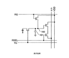
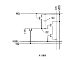
図3で、米国特許第6,730,897号(特許文献1)は、浮遊拡散ノード160と接地との間に接続されるキャパシタ161を付加することによって浮遊拡散ノード160のキャパシタンスを増大させることを開示する。図4で、米国特許第6,960,796号(特許文献2)は、浮遊拡散ノード162と電源VDDとの間に接続されるキャパシタ163を付加することによって浮遊拡散ノード162のキャパシタンスを増大させることを開示する。先行技術は、最大出力電圧が最大フォトダイオード電荷容量での電源限界範囲内にあることを確かにするほど十分に浮遊拡散ノードのキャパシタンスを増大させる。しかし、先行技術の解決法は、低光レベル状態に関しては最適でない。フォトダイオードに極めて少量の電荷がある場合に、浮遊拡散ノードのキャパシタンスが大きければ大きいほど電圧出力は低くなり、小さい信号を測定することが困難となる。低光レベルでのイメージングにおいては(増大した電圧出力のための)小さい浮遊拡散キャパシタンスを有し、高光レベルでのイメージングにおいては(電源範囲を下回って電圧出力を低めるほど)大きい浮遊拡散キャパシタンスを有するニーズが存在する。これは、画素内ゲイン制御の形である。
In FIG. 3, US Pat. No. 6,730,897 increases the capacitance of the
図5は、浮遊拡散ノード166に接続されている余分の“ダングリング(dangling)”トランジスタ165を備える画素を示す。この画素は、米国特許出願公開第2006/0103749(A1)号(特許文献3)に示されている。AUX信号線によりトランジスタ165をオンに切り替えることで、浮遊拡散ノード166のキャパシタンスは増大する。浮遊拡散キャパシタンスのこのような変更方法は、浮遊拡散ノード166の近くでノード166に直接的に電気的に接続される4つのトランジスタゲート165、167、168及び169を必要とする。4つのトランジスタゲートの存在により、最小の可能な浮遊拡散ノードキャパシタンスは可能でない。トランジスタ165がオフされる場合に、ゲートは、3つのトランジスタしか浮遊拡散ノードに隣接しない場合に比べて、依然として幾らかの付加的なキャパシタンスを加える。
FIG. 5 shows a pixel with an extra “dangling”
米国特許第7,075,049号(特許文献4)も浮遊拡散ノードのキャパシタンスを変える能力を備える画素を示す。それは、同じく、浮遊拡散ノードに隣接する4つのトランジスタの必要性を有する。従って、特許文献4の画素設計は、最小の可能な浮遊拡散キャパシタンスを提供しない。 US Pat. No. 7,075,049 also shows a pixel with the ability to change the capacitance of a floating diffusion node. It also has the need for four transistors adjacent to the floating diffusion node. Thus, the pixel design of US Pat.
本発明は、浮遊拡散キャパシタンスを変更可能な画素を開示する。更に、本発明は、浮遊拡散ノードに隣接するトランジスタゲートを3つしか必要とせず、画素に加えられる付加的な信号線を必要としない。 The present invention discloses a pixel capable of changing the floating diffusion capacitance. Furthermore, the present invention requires only three transistor gates adjacent to the floating diffusion node and does not require additional signal lines added to the pixel.
本発明は、上記の問題のうちの1又はそれ以上を解決することを目的とする。 The present invention is directed to overcoming one or more of the problems set forth above.
簡潔に述べると、本発明の一側面に従って、画像信号を読み出す方法であって、少なくとも2つの光感受領域を設けるステップと、前記少なくとも2つの光感受領域の夫々に各自関連する少なくとも2つのトランスファーゲートを設けるステップと、前記少なくとも2つのトランスファーゲートに電気的に接続されるコモン電荷−電圧変換領域を設けるステップと、前記コモン電荷−電圧変換領域をリセットするリセットメカニズムを設けるステップと、前記少なくとも2つの光感受領域のうち少なくとも1つの光感受領域から電荷を運んだ後、第1の時点で前記少なくとも2つのトランスファーゲートの全てを無効にするステップと、続く第2の時点で少なくとも1つのトランスファーゲートを有効にするステップと、前記第2の時点から前記少なくとも1つのトランスファーゲートが有効なままである間、続く第3の時点で前記少なくとも2つの光感受領域のうち少なくとも1つの光感受領域から電荷を運ぶステップとを有する方法が記載される。 Briefly described, according to one aspect of the present invention, there is provided a method for reading an image signal, the method comprising providing at least two photosensitive areas, and at least two transfer gates each associated with each of the at least two photosensitive areas. Providing a common charge-voltage conversion region electrically connected to the at least two transfer gates, providing a reset mechanism for resetting the common charge-voltage conversion region, and the at least two After carrying charge from at least one of the photosensitive regions, disabling all of the at least two transfer gates at a first time, and at least one transfer gate at a subsequent second time The enabling step and from the second time point During serial remain least one transfer gate is enabled, the method comprising the steps of carrying charge from at least one light sensitive region of the subsequent said at least two light sensitive region in the third time is described.
本発明の上記の及び他の目的は、以下の記載及び図面に関連してより明らかになるであろう。図面において、同じ参照番号は、可能であれば、各図に共通する同じ要素を示すために使用される。 The above and other objects of the present invention will become more apparent in connection with the following description and drawings. In the drawings, the same reference numerals will be used, where possible, to indicate the same elements common to the figures.
本発明は、浮遊拡散ノードに隣接するトランジスタゲートを3つしか有さない可変ゲイン制御に係る下記の利点を有し、付加的な信号線を必要としない。 The present invention has the following advantages related to variable gain control having only three transistor gates adjacent to a floating diffusion node, and does not require an additional signal line.
本発明について詳細に論じる前に、留意すべきは、本発明は、望ましくはCMOSアクティブ画素センサで用いられるが、それに限定されない点である。アクティブ画素センサは、スイッチとして機能するトランジスタ以外の、画素内の能動電気素子をいう。例えば、浮遊拡散(floating diffusion)又は増幅器は能動素子である。CMOSは、画素に関連するが一般的に画素にはなく、トランジスタのソース/ドレインが1つのドーパントタイプ(例えば、pタイプ)であり且つそれと対のトランジスタが反対のドーパントタイプ(例えば、nタイプ)である場合に形成される相補型金属酸化膜シリコンタイプの電気部品(例えば、トランジスタ)をいう。CMOSデバイスは、電力消費が少ないという一利点を含む幾つかの利点を有する。 Before discussing the present invention in detail, it should be noted that the present invention is preferably used in, but not limited to, CMOS active pixel sensors. An active pixel sensor refers to an active electrical element in a pixel other than a transistor that functions as a switch. For example, floating diffusion or an amplifier is an active device. CMOS is related to the pixel but is not generally in the pixel, and the source / drain of the transistor is of one dopant type (eg, p-type) and the opposite transistor type (eg, n-type). In other words, the complementary metal oxide silicon type electrical component (for example, a transistor) is formed. CMOS devices have several advantages, including one advantage of low power consumption.
図6は、本発明を実施可能なCMOS画素200を示す。CMOS画素200は、フォトダイオード201及び202として示されている2つの光感受領域を有する。各フォトダイオード201及び202は、トランスファーゲート203及び204によってコモン電荷−電圧変換ノード205に接続されている。リセットトランジスタ206は、電荷−電圧変換ノード205を電源電圧210に設定するために使用される。出力トランジスタ207は、行選択トランジスタ208が有効にされる場合に出力信号線209を駆動するために使用される。
FIG. 6 shows a
図7は、製造された画素200の水平断面を示す。トランスファーゲート204及び203は、電荷−電圧変換ノード205として働く埋め込み拡散を囲むように示されている。フォトダイオード埋め込み201及び202は、表面ピンニング層埋め込み211の下にある。このようなフォトダイオードは、一般に、ピンフォトダイオード(pinned photodiode)と呼ばれる。各画素の上には、同じ又は異なる色から成るカラーフィルタ材料220及び221がある。マイクロレンズ222及び223の配列は、画素のフォトダイオード領域に光線224の焦点を合わせる。
FIG. 7 shows a horizontal cross section of the manufactured
図7の断面の下には、画素200の種々の領域の下での電気チャネルポテンシャルが示されている。231は、トランスファーゲート204がオフ状態にある場合のトランスファーゲート204の下のチャネルポテンシャルである。233は、トランスファーゲート203がオフ状態にある場合にトランスファーゲート203の下のチャネルポテンシャルである。232は、(図6に示されるように)ノード205がトランジスタ206によってリセットされた後の電荷−電圧変換ノード205のチャネルポテンシャルである。領域230及び234は、フォトダイオード201及び202での光発生電荷の量を表す。
Below the cross-section of FIG. 7, the electrical channel potential under various regions of the
図8には、フォトダイオード201及び202で光発生電荷230及び234をサンプリングする種々の時点での図7のチャネルポテンシャル図のみが示されている。フォトダイオード201及び202で光発生電荷230及び234をサンプリングする過程は、時間ステップT0で始まる。時間ステップT0で、1つのフォトダイオード電荷230は、他のフォトダイオード電荷234より小さい。
FIG. 8 shows only the channel potential diagram of FIG. 7 at various points in time when the
電荷の差の原因は、例えば、フォトダイオード202がより長い積分時間を有すること、あるいは、カラーフィルタ221がより透明であり又はより幅広い色を通すことによって引き起こされ得る。マイクロレンズ223は、また、マイクロレンズ222よりも多くの光を収集するよう製造されてよい。これらの特徴のいずれも、本発明に組み込まれてよい。時間ステップT0は、電荷−電圧変換領域205がチャネルポテンシャル232にリセットされた後である。電荷−電圧変換領域205のリセット電圧もこの時点にサンプリングされる。時間ステップT1で、トランスファーゲート204は、電荷230を電荷−電圧変換領域205に運ぶようオンされる。次に、時間ステップT2で、トランスファーゲート204はオフされ、電荷−電圧変換領域205での新たな電圧は、電荷230の量を測定するようサンプリングされてリセット電圧レベルから減じられる。時間ステップT3で、電荷−電圧変換領域205は再びリセットされ、リセット電圧レベルがサンプリングされる。時間ステップT4で、トランスファーゲート204は、電荷−電圧変換領域205のキャパシタンスを増大させる電圧レベルへとオンされる。電荷−電圧変換領域205は、時間ステップT3に代えて時間ステップT4でリセットされてよい。トランスファーゲート204は、トランスファーゲート203も電荷234を電荷−電圧変換領域205に運ぶよう時間ステップT5でオンされる場合に、依然としてオンである。トランスファーゲート203が時間ステップT6でオフされる場合に、電荷234は、トランスファーゲート204が時間ステップT2でオフされた場合よりも高いキャパシタンスを有するより大きな領域にわたって散開する。
The cause of the charge difference can be caused, for example, by the
この場合に、電荷Q、キャパシタンスC、及び電圧Vの間の関係を考える。なお、VはV=Q/Cによって与えられる。キャパシタンスが高いほど電荷−電圧変換領域205での電圧変化は小さいので、電荷−電圧変換領域205はより多くの量の電荷を保持することができる。より高いキャパシタンスは、より低い電荷−電圧変換ゲインに対応する。このようにして、本発明は、いずれのトランスファーゲートもオフされている状態で高いゲインを有して少量の電荷をサンプリングすることができ、且つ、トランスファーゲートの1つがオンされている状態で大量の電荷をサンプリングすることもできる。
In this case, consider the relationship between charge Q, capacitance C, and voltage V. Note that V is given by V = Q / C. Since the voltage change in the charge-
最後にほとんどの電荷を有してフォトダイオードから電荷を運ぶことが有利である。これは、それが、電荷−電圧変換領域が空のフォトダイオードからトランスファーゲートをオンすることで最も高いキャパシタンスを有することができる時点であることによる。また、本発明は、2よりも多いフォトダイオードを共有する画素に拡張され得ることは明白である。また、2よりも多いフォトダイオードを有して、電荷−電圧変換領域のキャパシタンス制御が2よりも多い多段階で行われ得ることも明白である。 Finally, it is advantageous to carry the charge from the photodiode with the most charge. This is because it is the point at which the charge-to-voltage conversion region can have the highest capacitance by turning on the transfer gate from an empty photodiode. It is also apparent that the present invention can be extended to pixels that share more than two photodiodes. It is also clear that with more than two photodiodes, capacitance control of the charge-voltage conversion region can be performed in more than two stages.
図9は、画素の出力電圧対フォトダイオードで収集される電荷の量を示す。電荷が、いずれのトランスファーゲートもオフされている状態でサンプリングされる場合に、画素は高ゲインモードにあり、低電荷レベルで飽和に達する出力電圧曲線240を出現させる。電荷が、1つのトランスファーゲートがオンされている状態でサンプリングされる場合に、画素は低ゲインモードにあり、より高い電荷レベルで飽和に達する出力電圧曲線241を出現させる。
FIG. 9 shows the amount of charge collected at the photodiode versus the output voltage of the pixel. When charge is sampled with any transfer gates off, the pixel is in a high gain mode, causing an
本発明の第2実施例で、画素構造は図7及び図8に示されるものと同じであるが、トランスファーゲートの動作は異なる。図10で、時間ステップT0は、電荷−電圧変換領域205がチャネルポテンシャル232にリセットされた後である。電荷−電圧変換領域205のリセット電圧は、また、この時点でサンプリングされる。時間ステップT1で、トランスファーゲート204は、電荷230を電荷−電圧変換領域205に運ぶようオンされる。次に、時間ステップT2で、トランスファーゲート204はオフされ、電荷−電圧変換領域205での新たな電圧は、電荷230の量を測定するようサンプリングされてリセット電圧レベルから減じられる。時間ステップT3で、電荷−電圧変換領域205は再びリセットされ、リセット電圧レベルがサンプリングされる。時間ステップT4で、トランスファーゲート204は、フォトダイオードのチャネルポテンシャルとリセット電圧レベルのチャネルポテンシャル232との間にトランスファーゲートのチャネルポテンシャル231を設定する電圧レベルへと部分的にオンされる。時間ステップT5で、トランスファーゲート203は、電荷234を電荷−電圧変換領域205に運ぶようオンされ、次いで、トランスファーゲート203は時間ステップT6でオフされる。
In the second embodiment of the present invention, the pixel structure is the same as that shown in FIGS. 7 and 8, but the operation of the transfer gate is different. In FIG. 10, the time step T 0 is after the charge-
トランスファーゲート204の部分的なターン・オンの利点は、電荷−電圧変換領域のキャパシタンスが小さい電荷については高く、大きい電荷については低いことである。図10は、電荷234が小さく、時間ステップT6でトランスファーゲート204のチャネルポテンシャル231を越えて電荷−電圧変換領域205を満たさない場合を示す。従って、この場合に、電荷234は、低キャパシタンス且つ高電圧変換ゲインを有して測定される。図11の場合に、電荷234は大きく、電荷234が電荷−電圧変換領域205に運ばれる場合に、電荷234は時間ステップT6でチャネルポテンシャル231より上を流れる。この場合に、大きな電荷234は、大きなキャパシタンス且つより低い電圧変換ゲインを有して測定される。
The advantage of partial turn-on of the
図12は、第2実施例での電荷−電圧変換領域205の電圧応答対フォトダイオードで収集される電荷の量を示す。電荷が点243を上回って大きい場合に、電圧応答のスロープは減少し、曲線244に続く。トランスファーゲート204が部分的にオンされるのではなくオフされている場合に、電圧応答は、より高いゲイン曲線242に従う。第2実施例は、低信号レベルでの高ゲイン及び高信号レベルでの低ゲインを可能にする。
FIG. 12 shows the voltage response of the charge-
本発明の第3実施例で、画素構造は図7及び図8に示されるものと同じであるが、トランスファーゲートの動作は異なる。本発明の第3実施例は図13に表される。時間ステップT0で、電荷−電圧変換領域205はまさにリセットされ、その電圧をV1としてサンプリングされる。時間T1で、トランスファーゲート204は、電荷230を電荷−電圧変換領域205に運ぶようオンされる。トランスファーゲート204が依然としてオンである間、電荷−電圧変換領域205の電圧はV2としてサンプリングされる。時間ステップT2で、トランスファーゲート204はオフされ、電荷−電圧変換領域205の電圧はV3としてサンプリングされる。
In the third embodiment of the present invention, the pixel structure is the same as that shown in FIGS. 7 and 8, but the operation of the transfer gate is different. A third embodiment of the invention is represented in FIG. At time step T0, the charge-to-
電圧V3−V1は、電荷230の高変換ゲイン測定を表す。電圧V2−V1は、電荷230の低変換ゲイン測定を表す。しかし、V2−V1は、電荷−電圧変換領域205へのトランスファーゲート204の容量結合によって引き起こされるオフセット誤差を含む。このオフセット誤差を除去するよう、電荷−電圧変換領域205は時間ステップT3で再びリセットされ、その電圧はV4として測定される。次に、時間ステップT4で、トランスファーゲート204は再びオンされ、電荷−電圧変換領域205の電圧がV5として測定される間、オンに保持される。V5を測定することで、フォトダイオード201に電荷がなかった場合に、オフセット誤差はV5−V4として得られる。この場合に、正しい低変換ゲイン測定はV2−V1−(V5−V4)である。
Voltage V3-V1 represents a high conversion gain measurement of
それほど正確でない測定に関して、電圧V4は無視され、V1がその代わりに用いられてよい。この場合に、低変換ゲイン測定はV2−V1−(V5−V1)、すなわち、V2−2V1−V5である。 For less accurate measurements, the voltage V4 is ignored and V1 may be used instead. In this case, the low conversion gain measurement is V2-V1- (V5-V1), ie, V2-2V1-V5.
第3実施例は、コモン電荷−電圧変換領域を共有する任意数のフォトダイオードを有するCMOSアクティブ画素に適用され得る。図13のステップは、フォトダイオードの夫々1つについて繰り返される。 The third embodiment can be applied to a CMOS active pixel having an arbitrary number of photodiodes sharing a common charge-voltage conversion region. The steps of FIG. 13 are repeated for each one of the photodiodes.
第3実施例の利点は、画像センサの全ての画素が高低両方の電荷−電圧変換ゲインによりサンプリングされる点である。本発明の全ての実施例の利点は、それらが何らのトランジスタ又は信号配線の付加も要しない点である。 The advantage of the third embodiment is that all pixels of the image sensor are sampled with both high and low charge-to-voltage conversion gains. An advantage of all embodiments of the present invention is that they do not require the addition of any transistors or signal lines.
図14は、トランスファーゲートが本発明の電荷−電圧変換ゲイン制御により動作する画素308を有する本発明のCMOSアクティブ画素画像センサ300を示す。画像センサ300の基本構成要素は、光感受画素308の配列である。行デコーダ回路305は、相関二重サンプリング(CDS)回路325によってサンプリングされる画素308の行全体を選択する。アナログ−デジタル変換器315は、列デコーダを横切って走査し、CDS325に記憶されている信号をデジタル化する。アナログ−デジタル変換器315は、各列をシリアルにデジタル化する1つの高速変換器又は列毎の1つの変換器(パラレル)を有するタイプであってよい。デジタル化されたデータは、直接的に画像センサ300から出力されてよく、あるいは、欠陥補正、カラーフィルタ補間、画像スケーリング、及び他の特別な効果のための集積画像処理320があってよい。タイミング発生器310は、画素配列の全体又は画素配列の一部のみをサンプリングするよう行デコーダ305及び列デコーダ325を制御する。
FIG. 14 shows a CMOS active
図15は、電子イメージングシステム、望ましくはデジタルカメラ400において、トランスファーゲートが電荷−電圧変換ゲイン制御により動作する画素を用いる画像センサ300を示す。
FIG. 15 shows an
本発明は、好ましい実施形態を参照して記載されてきた。しかし、当然のことながら、変形及び改良は、本発明の技術的範囲から外れることなく、当該技術で通常の知識を有する者によって行われ得る。 The invention has been described with reference to the preferred embodiments. However, it will be appreciated that variations and modifications can be effected by persons having ordinary skill in the art without departing from the scope of the present invention.
100,300 画像センサ
105,305 行デコーダ回路
110,310 タイミング発生器
115,315 アナログ−デジタル変換器
120,320 集積画像処理
125,325 相関二重サンプリング(CDS)回路
130,308 光感受画素
150,206 リセットトランジスタ
151 フォトダイオード
152 トランスファートランジスタ
153,207 出力トランジスタ
154,208 行選択トランジスタ
155,160,162,166 浮遊拡散ノード
161,163 キャパシタ
165 ダングリングトランジスタゲート
167,168,169 トランジスタゲート
200 画素
201,202 フォトダイオード埋め込み
203,204 トランスファーゲート
205 電荷−電圧変換ノード
209 出力信号線
210 電源電圧
211 表面ピンニング層埋め込み/ピンフォトダイオード
220,221 カラーフィルタ材質
222,223 マイクロレンズ
224 光線
230,234 光発生電荷(フォトダイオード)
231,232,233 チャネルポテンシャル
240,241 出力電圧曲線
242 高ゲイン曲線
243 点
244 曲線
400 デジタルカメラ
100, 300
231, 232, 233 Channel potential 240, 241
Claims (2)
少なくとも2つの光感受領域を設けるステップと、
前記少なくとも2つの光感受領域の夫々に各自関連する少なくとも2つのトランスファーゲートを設けるステップと、
前記少なくとも2つのトランスファーゲートに電気的に接続されるコモン電荷−電圧変換領域を設けるステップと、
前記コモン電荷−電圧変換領域をリセットするリセットメカニズムを設けるステップと、
前記少なくとも2つの光感受領域のうち少なくとも1つの光感受領域から電荷を運んだ後、第1の時点で前記少なくとも2つのトランスファーゲートの全てを無効にするステップと、
続く第2の時点で少なくとも1つのトランスファーゲートを有効にするステップと、
前記第2の時点から前記少なくとも1つのトランスファーゲートが有効なままである間、続く第3の時点で前記少なくとも2つの光感受領域のうち少なくとも1つの他の光感受領域から電荷を運ぶステップとを含み、
前記第2の時点と前記第3の時点との間に前記コモン電荷−電圧変換領域をリセットするステップを更に含む、方法。 A method for reading an image signal,
Providing at least two light sensitive areas;
Providing at least two transfer gates associated with each of the at least two photosensitive regions;
Providing a common charge-voltage conversion region electrically connected to the at least two transfer gates;
Providing a reset mechanism for resetting the common charge-voltage conversion region;
Disabling all of the at least two transfer gates at a first time after carrying charge from at least one of the at least two photosensitive regions;
Enabling at least one transfer gate at a subsequent second time point;
Wherein the second time point at least one transfer gate remains valid between, and a step of carrying at least one other charge from the light sensitive region of the third time following at least two light sensitive area Including
Resetting the common charge-to-voltage conversion region between the second time point and the third time point .
より高い光感受性を有する前記少なくとも2つの光感受領域のうち少なくとも1つの他の光感受領域から前記第3の時点に電荷を運ぶステップと
を更に含む請求項1記載の方法。 Providing at least two different light sensitivities to the at least two light sensitive areas;
The method of claim 1, further comprising: carrying charge from the at least one other light sensitive area of the at least two light sensitive areas having a higher light sensitivity to the third time point.
Applications Claiming Priority (3)
| Application Number | Priority Date | Filing Date | Title |
|---|---|---|---|
| US11/742,883 | 2007-05-01 | ||
| US11/742,883 US8159585B2 (en) | 2007-05-01 | 2007-05-01 | Image sensor pixel with gain control |
| PCT/US2008/005148 WO2008133861A1 (en) | 2007-05-01 | 2008-04-22 | Image sensor pixel with gain control |
Publications (3)
| Publication Number | Publication Date |
|---|---|
| JP2010526479A JP2010526479A (en) | 2010-07-29 |
| JP2010526479A5 JP2010526479A5 (en) | 2011-06-16 |
| JP5230726B2 true JP5230726B2 (en) | 2013-07-10 |
Family
ID=39473856
Family Applications (1)
| Application Number | Title | Priority Date | Filing Date |
|---|---|---|---|
| JP2010506226A Active JP5230726B2 (en) | 2007-05-01 | 2008-04-22 | Image sensor pixel with gain control |
Country Status (7)
| Country | Link |
|---|---|
| US (2) | US8159585B2 (en) |
| EP (2) | EP2150038B1 (en) |
| JP (1) | JP5230726B2 (en) |
| KR (1) | KR101388276B1 (en) |
| CN (1) | CN101675657B (en) |
| TW (1) | TWI450579B (en) |
| WO (1) | WO2008133861A1 (en) |
Families Citing this family (17)
| Publication number | Priority date | Publication date | Assignee | Title |
|---|---|---|---|---|
| WO2009136285A2 (en) * | 2008-04-16 | 2009-11-12 | Quantum Semiconductor Llc | Pixel circuitry for ultra wide dynamic range |
| JP4538528B2 (en) | 2008-12-26 | 2010-09-08 | 廣津 和子 | Solid-state image sensor |
| US8411184B2 (en) * | 2009-12-22 | 2013-04-02 | Omnivision Technologies, Inc. | Column output circuits for image sensors |
| US9000500B2 (en) * | 2009-12-30 | 2015-04-07 | Omnivision Technologies, Inc. | Image sensor with doped transfer gate |
| FR2995725A1 (en) * | 2012-09-19 | 2014-03-21 | St Microelectronics Sa | Method for controlling pixel in complementary metal oxide semiconductor image sensor, involves reading information representative of potential of reading point during initial period of closing of metal oxide semiconductor transistor |
| CN102843524B (en) * | 2012-09-25 | 2015-09-23 | 中国科学院上海高等研究院 | Cmos image sensor and method of work thereof |
| CN105165005B (en) * | 2013-03-14 | 2020-03-27 | 株式会社尼康 | Imaging unit, imaging device, and imaging control program |
| US9578223B2 (en) | 2013-08-21 | 2017-02-21 | Qualcomm Incorporated | System and method for capturing images with multiple image sensing elements |
| US9160958B2 (en) | 2013-12-18 | 2015-10-13 | Omnivision Technologies, Inc. | Method of reading out an image sensor with transfer gate boost |
| JP6254048B2 (en) * | 2014-06-05 | 2017-12-27 | ルネサスエレクトロニクス株式会社 | Semiconductor device |
| KR102591364B1 (en) | 2015-09-23 | 2023-10-19 | 삼성디스플레이 주식회사 | Photo sensor and display device including the same |
| CN105681692B (en) * | 2016-01-11 | 2018-10-30 | 珠海艾思克科技有限公司 | Cmos image sensor and its reset noise appraisal procedure |
| DE102016212784A1 (en) * | 2016-07-13 | 2018-01-18 | Robert Bosch Gmbh | CMOS pixel, image sensor and camera and method for reading out a CMOS pixel |
| JP6420450B2 (en) * | 2017-11-29 | 2018-11-07 | ルネサスエレクトロニクス株式会社 | Semiconductor device |
| US11317038B2 (en) | 2017-12-19 | 2022-04-26 | SmartSens Technology (HK) Co., Ltd. | Pixel unit with a design for half row reading, an imaging apparatus including the same, and an imaging method thereof |
| JP7299680B2 (en) * | 2018-08-23 | 2023-06-28 | キヤノン株式会社 | Imaging device and imaging system |
| KR20220101694A (en) | 2019-11-20 | 2022-07-19 | 기가조트 테크널러지 인코포레이티드 | Scalable pixel size image sensor |
Family Cites Families (21)
| Publication number | Priority date | Publication date | Assignee | Title |
|---|---|---|---|---|
| JPH05251480A (en) * | 1992-03-04 | 1993-09-28 | Sony Corp | Charge voltage converter |
| JP2000152086A (en) * | 1998-11-11 | 2000-05-30 | Canon Inc | Image pickup device and image pickup system |
| JP3592106B2 (en) * | 1998-11-27 | 2004-11-24 | キヤノン株式会社 | Solid-state imaging device and camera |
| US6730897B2 (en) * | 2000-12-29 | 2004-05-04 | Eastman Kodak Company | Linearity and dynamic range for complementary metal oxide semiconductor active pixel image sensors |
| US6960796B2 (en) * | 2002-11-26 | 2005-11-01 | Micron Technology, Inc. | CMOS imager pixel designs with storage capacitor |
| JP2004336469A (en) * | 2003-05-08 | 2004-11-25 | Fuji Film Microdevices Co Ltd | Solid-state imaging element, imaging apparatus, and image processing method |
| US7075049B2 (en) | 2003-06-11 | 2006-07-11 | Micron Technology, Inc. | Dual conversion gain imagers |
| US7026596B2 (en) * | 2003-10-30 | 2006-04-11 | Micron Technology, Inc. | High-low sensitivity pixel |
| US7091531B2 (en) * | 2004-04-07 | 2006-08-15 | Micron Technology, Inc. | High dynamic range pixel amplifier |
| JP4317115B2 (en) * | 2004-04-12 | 2009-08-19 | 国立大学法人東北大学 | Solid-state imaging device, optical sensor, and operation method of solid-state imaging device |
| JP4380439B2 (en) * | 2004-07-16 | 2009-12-09 | ソニー株式会社 | Data processing method, data processing apparatus, semiconductor device for detecting physical quantity distribution, and electronic apparatus |
| KR100656666B1 (en) | 2004-09-08 | 2006-12-11 | 매그나칩 반도체 유한회사 | Image sensor |
| US7193198B2 (en) | 2004-10-01 | 2007-03-20 | Omnivision Technologies, Inc. | Image sensor and pixel that has variable capacitance output or floating node |
| US20060103749A1 (en) * | 2004-11-12 | 2006-05-18 | Xinping He | Image sensor and pixel that has switchable capacitance at the floating node |
| US7830437B2 (en) * | 2005-05-11 | 2010-11-09 | Aptina Imaging Corp. | High fill factor multi-way shared pixel |
| US7238926B2 (en) * | 2005-06-01 | 2007-07-03 | Eastman Kodak Company | Shared amplifier pixel with matched coupling capacitances |
| KR101010489B1 (en) | 2005-06-21 | 2011-01-21 | 미츠비시덴키 가부시키가이샤 | Programming system for program executing system and program constructing system for examination device |
| US7432540B2 (en) * | 2005-08-01 | 2008-10-07 | Micron Technology, Inc. | Dual conversion gain gate and capacitor combination |
| JP4747781B2 (en) * | 2005-10-27 | 2011-08-17 | 船井電機株式会社 | Imaging device |
| JP4650249B2 (en) * | 2005-12-13 | 2011-03-16 | 船井電機株式会社 | Imaging device |
| JP4747858B2 (en) * | 2006-01-27 | 2011-08-17 | 船井電機株式会社 | Imaging device |
-
2007
- 2007-05-01 US US11/742,883 patent/US8159585B2/en active Active
-
2008
- 2008-04-22 EP EP09176344.1A patent/EP2150038B1/en active Active
- 2008-04-22 JP JP2010506226A patent/JP5230726B2/en active Active
- 2008-04-22 EP EP08743163.1A patent/EP2140676B1/en active Active
- 2008-04-22 WO PCT/US2008/005148 patent/WO2008133861A1/en active Application Filing
- 2008-04-22 CN CN200880014156.8A patent/CN101675657B/en active Active
- 2008-04-22 KR KR1020097022858A patent/KR101388276B1/en active IP Right Grant
- 2008-04-30 TW TW097116019A patent/TWI450579B/en active
-
2012
- 2012-03-12 US US13/418,182 patent/US8717476B2/en active Active
Also Published As
| Publication number | Publication date |
|---|---|
| EP2150038A2 (en) | 2010-02-03 |
| JP2010526479A (en) | 2010-07-29 |
| CN101675657A (en) | 2010-03-17 |
| CN101675657B (en) | 2014-09-10 |
| EP2140676A1 (en) | 2010-01-06 |
| TWI450579B (en) | 2014-08-21 |
| TW200922284A (en) | 2009-05-16 |
| EP2140676B1 (en) | 2015-08-19 |
| EP2150038A3 (en) | 2012-05-30 |
| WO2008133861A1 (en) | 2008-11-06 |
| US8159585B2 (en) | 2012-04-17 |
| US20080273104A1 (en) | 2008-11-06 |
| US8717476B2 (en) | 2014-05-06 |
| EP2150038B1 (en) | 2013-06-12 |
| KR101388276B1 (en) | 2014-04-22 |
| KR20100016124A (en) | 2010-02-12 |
| US20120168611A1 (en) | 2012-07-05 |
Similar Documents
| Publication | Publication Date | Title |
|---|---|---|
| JP5230726B2 (en) | Image sensor pixel with gain control | |
| US20240313012A1 (en) | Imaging device including photoelectric converters and capacitor | |
| US7468501B2 (en) | Linear dynamic range enhancement in a CMOS imager | |
| KR101398767B1 (en) | Reduced pixel area image sensor | |
| US7427790B2 (en) | Image sensor with gain control | |
| US20060266922A1 (en) | Pinned-photodiode pixel with global shutter | |
| JP2010016056A (en) | Photoelectric conversion device | |
| JP2006216907A (en) | Solid state imaging device | |
| KR100801758B1 (en) | Image sensor and controlling method thereof | |
| CN210168124U (en) | Image sensor with a plurality of pixels | |
| US6882022B2 (en) | Dual gate BCMD pixel suitable for high performance CMOS image sensor arrays | |
| JP2008053333A (en) | Solid-state imaging device | |
| US10880500B2 (en) | Pixel apparatus and CMOS image sensor using the same | |
| KR100962470B1 (en) | Pixel circuit in the solid state image sensing device | |
| JP4320693B2 (en) | Solid-state imaging device | |
| JP4718169B2 (en) | CMOS imaging device circuit | |
| JP2006147709A (en) | Imaging device | |
| JP4345145B2 (en) | Solid-state imaging device | |
| JP2011199050A (en) | Solid-state imaging device and electronic apparatus | |
| JP5868451B2 (en) | Photoelectric conversion device |
Legal Events
| Date | Code | Title | Description |
|---|---|---|---|
| A521 | Request for written amendment filed |
Free format text: JAPANESE INTERMEDIATE CODE: A523 Effective date: 20110419 |
|
| A621 | Written request for application examination |
Free format text: JAPANESE INTERMEDIATE CODE: A621 Effective date: 20110419 |
|
| A711 | Notification of change in applicant |
Free format text: JAPANESE INTERMEDIATE CODE: A711 Effective date: 20110530 |
|
| A977 | Report on retrieval |
Free format text: JAPANESE INTERMEDIATE CODE: A971007 Effective date: 20120724 |
|
| A131 | Notification of reasons for refusal |
Free format text: JAPANESE INTERMEDIATE CODE: A131 Effective date: 20120731 |
|
| A521 | Request for written amendment filed |
Free format text: JAPANESE INTERMEDIATE CODE: A523 Effective date: 20121030 |
|
| TRDD | Decision of grant or rejection written | ||
| A01 | Written decision to grant a patent or to grant a registration (utility model) |
Free format text: JAPANESE INTERMEDIATE CODE: A01 Effective date: 20130305 |
|
| A61 | First payment of annual fees (during grant procedure) |
Free format text: JAPANESE INTERMEDIATE CODE: A61 Effective date: 20130319 |
|
| FPAY | Renewal fee payment (event date is renewal date of database) |
Free format text: PAYMENT UNTIL: 20160329 Year of fee payment: 3 |
|
| R150 | Certificate of patent or registration of utility model |
Ref document number: 5230726 Country of ref document: JP Free format text: JAPANESE INTERMEDIATE CODE: R150 Free format text: JAPANESE INTERMEDIATE CODE: R150 |
|
| R250 | Receipt of annual fees |
Free format text: JAPANESE INTERMEDIATE CODE: R250 |
|
| R250 | Receipt of annual fees |
Free format text: JAPANESE INTERMEDIATE CODE: R250 |
|
| R250 | Receipt of annual fees |
Free format text: JAPANESE INTERMEDIATE CODE: R250 |
|
| R250 | Receipt of annual fees |
Free format text: JAPANESE INTERMEDIATE CODE: R250 |
|
| R250 | Receipt of annual fees |
Free format text: JAPANESE INTERMEDIATE CODE: R250 |
|
| R250 | Receipt of annual fees |
Free format text: JAPANESE INTERMEDIATE CODE: R250 |
|
| R250 | Receipt of annual fees |
Free format text: JAPANESE INTERMEDIATE CODE: R250 |
|
| R250 | Receipt of annual fees |
Free format text: JAPANESE INTERMEDIATE CODE: R250 |
|
| R250 | Receipt of annual fees |
Free format text: JAPANESE INTERMEDIATE CODE: R250 |