JP5224735B2 - Liquid crystal device and electronic device - Google Patents
Liquid crystal device and electronic device Download PDFInfo
- Publication number
- JP5224735B2 JP5224735B2 JP2007171634A JP2007171634A JP5224735B2 JP 5224735 B2 JP5224735 B2 JP 5224735B2 JP 2007171634 A JP2007171634 A JP 2007171634A JP 2007171634 A JP2007171634 A JP 2007171634A JP 5224735 B2 JP5224735 B2 JP 5224735B2
- Authority
- JP
- Japan
- Prior art keywords
- voltage
- line
- scanning line
- circuit
- scanning
- Prior art date
- Legal status (The legal status is an assumption and is not a legal conclusion. Google has not performed a legal analysis and makes no representation as to the accuracy of the status listed.)
- Expired - Fee Related
Links
Images


Landscapes
- Liquid Crystal Display Device Control (AREA)
- Control Of Indicators Other Than Cathode Ray Tubes (AREA)
- Liquid Crystal (AREA)
- Shift Register Type Memory (AREA)
Description
本発明は、液晶装置、および電子機器に関する。 The present invention relates to a liquid crystal device and an electronic apparatus.
従来より、表示装置として液晶装置が知られている。この液晶装置は、例えば、液晶パネルと、この液晶パネルに光を供給するバックライトと、を備える。 Conventionally, a liquid crystal device is known as a display device. The liquid crystal device includes, for example, a liquid crystal panel and a backlight that supplies light to the liquid crystal panel.
液晶パネルは、素子基板と、この素子基板に対向配置された対向基板と、素子基板と対向基板との間に設けられた液晶と、を備える。 The liquid crystal panel includes an element substrate, a counter substrate disposed opposite to the element substrate, and a liquid crystal provided between the element substrate and the counter substrate.
素子基板は、所定間隔おきに交互に設けられた複数の走査線および複数の容量線と、これら複数の走査線および複数の容量線に交差し所定間隔おきに設けられた複数のデータ線と、複数の走査線に接続された走査線駆動回路と、複数のデータ線に接続されたデータ線駆動回路と、複数の容量線に接続された容量線駆動回路と、を有する。 The element substrate includes a plurality of scanning lines and a plurality of capacitance lines alternately provided at predetermined intervals, a plurality of data lines which intersect the plurality of scanning lines and the plurality of capacitance lines and are provided at predetermined intervals, A scanning line driving circuit connected to the plurality of scanning lines; a data line driving circuit connected to the plurality of data lines; and a capacitance line driving circuit connected to the plurality of capacitance lines.
各走査線と各データ線との交差部分には、画素が設けられている。画素は、画素電極および共通電極からなる画素容量と、スイッチング素子としての薄膜トランジスタ(以降、TFT(Thin Film Transistor)と呼ぶ)と、一方の電極が容量線に接続され他方の電極が画素電極に接続された蓄積容量と、を備える。この画素は、マトリクス状に複数配列されて表示領域を形成する。 Pixels are provided at intersections between the scanning lines and the data lines. A pixel is composed of a pixel capacitor composed of a pixel electrode and a common electrode, a thin film transistor (hereinafter referred to as TFT (Thin Film Transistor)) as a switching element, one electrode connected to a capacitor line, and the other electrode connected to a pixel electrode. Storage capacity. A plurality of pixels are arranged in a matrix to form a display area.
TFTのゲートには、走査線が接続され、TFTのソースには、データ線が接続され、TFTのドレインには、画素電極および蓄積容量の他方の電極が接続されている。 A scanning line is connected to the gate of the TFT, a data line is connected to the source of the TFT, and a pixel electrode and the other electrode of the storage capacitor are connected to the drain of the TFT.
容量線駆動回路は、所定の電圧を各容量線に供給する。 The capacitor line driving circuit supplies a predetermined voltage to each capacitor line.
走査線駆動回路は、走査線を選択する選択電圧(第1の選択電圧)を所定の順番で各走査線に供給する。走査線に第1の選択電圧が供給されると、この走査線に接続されたTFTが全てオン状態となる。 The scanning line driving circuit supplies a selection voltage (first selection voltage) for selecting a scanning line to each scanning line in a predetermined order. When the first selection voltage is supplied to the scanning line, all TFTs connected to the scanning line are turned on.
データ線駆動回路は、画像信号を各データ線に供給し、オン状態のTFTを介して、この画像信号に基づく画像電圧を画素電極に書き込む。 The data line driving circuit supplies an image signal to each data line, and writes an image voltage based on the image signal to the pixel electrode via the TFT in the on state.
ここで、データ線駆動回路は、共通電極の電圧よりも電位の高い電圧(以降、正極性と呼ぶ)の画像信号をデータ線に供給して、この正極性の画像信号に基づく画像電圧を画素電極に書き込む正極性書込と、共通電極の電圧よりも電位の低い電圧(以降、負極性と呼ぶ)の画像信号をデータ線に供給して、この負極性の画像信号に基づく画像電圧を画素電極に書き込む負極性書込と、を交互に行う。 Here, the data line driving circuit supplies an image signal having a voltage (hereinafter referred to as positive polarity) having a potential higher than that of the common electrode to the data line, and an image voltage based on the positive polarity image signal is supplied to the pixel. Positive polarity writing to be written to the electrodes, and an image signal having a voltage lower than the common electrode voltage (hereinafter referred to as negative polarity) is supplied to the data line, and the image voltage based on the negative polarity image signal is supplied to the pixel. Negative polarity writing to the electrodes is alternately performed.
対向基板は、各画素に対応して、R(赤)、G(緑)、B(青)といったカラーフィルタを有する。 The counter substrate has color filters such as R (red), G (green), and B (blue) corresponding to each pixel.
以上の液晶装置は、以下のように動作する。 The above liquid crystal device operates as follows.
すなわち、走査線に第1の選択電圧を順次供給することで、ある走査線に接続されたTFTを全てオン状態にして、この走査線に係る画素を全て選択する。そして、これら画素の選択に同期して、データ線に画像信号を供給する。すると、選択した全ての画素に、オン状態のTFTを介して画像信号が供給され、この画像信号に基づく画像電圧が画素電極に書き込まれる。 That is, by sequentially supplying the first selection voltage to the scanning line, all TFTs connected to the certain scanning line are turned on, and all the pixels related to the scanning line are selected. Then, an image signal is supplied to the data line in synchronization with the selection of these pixels. Then, an image signal is supplied to all the selected pixels via the on-state TFTs, and an image voltage based on the image signal is written to the pixel electrode.
画素電極に画像電圧が書き込まれると、画素電極と共通電極との電位差により、液晶に駆動電圧が印加される。液晶に駆動電圧が印加されると、液晶の配向や秩序が変化して、液晶を透過するバックライトからの光が変化する。この変化した光がカラーフィルタを透過することで、階調表示が行われる。 When an image voltage is written to the pixel electrode, a driving voltage is applied to the liquid crystal due to a potential difference between the pixel electrode and the common electrode. When a driving voltage is applied to the liquid crystal, the alignment and order of the liquid crystal change, and the light from the backlight that transmits the liquid crystal changes. The changed light passes through the color filter, so that gradation display is performed.
なお、液晶に印加される駆動電圧は、蓄積容量により、画像電圧が書き込まれる期間よりも3桁も長い期間に亘って保持される。 Note that the driving voltage applied to the liquid crystal is held by a storage capacitor for a period that is three orders of magnitude longer than the period during which the image voltage is written.
ところで、以上のような液晶装置は、例えば、携帯機器に用いられるが、この携帯機器では、近年、消費電力の低減が要請されている。そこで、画像電圧を画素電極に書き込んだ後に、TFTをオフ状態にするとともに容量線の電圧を変動させることで、消費電力を低減できる液晶装置が提案されている(例えば、特許文献1参照)。 By the way, the liquid crystal device as described above is used in, for example, a portable device. In this portable device, in recent years, reduction of power consumption is required. Therefore, a liquid crystal device has been proposed that can reduce power consumption by turning off the TFT and changing the voltage of the capacitor line after writing the image voltage to the pixel electrode (see, for example, Patent Document 1).
特許文献1のような容量線の電圧を変動させる液晶装置の動作について、図12、図13を用いて説明する。
The operation of the liquid crystal device that varies the voltage of the capacitor line as in
図12は、従来例に係る液晶装置の正極性書込時のタイミングチャートである。図13は、従来例に係る液晶装置の負極性書込時のタイミングチャートである。 FIG. 12 is a timing chart at the time of positive polarity writing of the liquid crystal device according to the conventional example. FIG. 13 is a timing chart at the time of negative polarity writing of the liquid crystal device according to the conventional example.
ここで、例えば、従来例に係る液晶装置は、320行の走査線および容量線と、240列のデータ線と、を有するものとする。 Here, for example, the liquid crystal device according to the conventional example has 320 rows of scanning lines and capacitance lines and 240 columns of data lines.
図12、図13において、GATE(m)は、320行の走査線のうちm行目(mは、1≦m≦320を満たす整数)の走査線の電圧であり、VST(m)は、320行の容量線のうちm行目の容量線の電圧である。また、SOURCE(n)は、240列のデータ線のうちn列目(nは、1≦n≦240を満たす整数)のデータ線の電圧である。また、PIX(m,n)は、m行目の走査線と、n列目のデータ線と、の交差に対応して設けられたm行n列目の画素が備える画素電極の電圧であり、VCOM(m)は、m行n列目の画素が備える共通電極の電圧である。 12 and 13, GATE (m) is the voltage of the scanning line of the m-th row (m is an integer satisfying 1 ≦ m ≦ 320) among the 320 scanning lines, and VST (m) is This is the voltage of the mth capacitor line among the 320th capacitor lines. SOURCE (n) is the voltage of the data line of the nth column (n is an integer satisfying 1 ≦ n ≦ 240) among the 240 data lines. PIX (m, n) is the voltage of the pixel electrode provided in the pixel in the mth row and the nth column provided corresponding to the intersection of the scanning line in the mth row and the data line in the nth column. , VCOM (m) is the voltage of the common electrode provided in the pixel in the m-th row and the n-th column.
まず、従来例に係る液晶装置の正極性書込時について、図12を用いて説明する。 First, the positive polarity writing of the liquid crystal device according to the conventional example will be described with reference to FIG.
時刻t51において、走査線駆動回路により、m行目の走査線に第1の選択電圧を供給する。すると、m行目の走査線の電圧GATE(m)は、上昇して、時刻t52では、電圧VGHとなる。これにより、m行目の走査線に接続されたTFTが全てオン状態となる。 At time t51, the first selection voltage is supplied to the m-th scanning line by the scanning line driving circuit. Then, the voltage GATE (m) of the m-th scanning line rises and becomes the voltage VGH at time t52. As a result, all TFTs connected to the m-th scanning line are turned on.
時刻t53において、データ線駆動回路により、n列目のデータ線に正極性の画像信号を供給する。すると、n列目のデータ線の電圧SOURCE(n)は、徐々に上昇して、時刻t54では、電圧VP8となる。 At time t53, the data line driving circuit supplies a positive image signal to the nth data line. Then, the voltage SOURCE (n) of the data line in the n-th column gradually increases and becomes voltage VP8 at time t54.
n列目のデータ線の電圧SOURCE(n)は、正極性の画像信号に基づく画像電圧として、m行目の走査線に接続されたオン状態のTFT51を介して、m行n列目の画素が備える画素電極に書き込まれる。このため、m行n列目の画素が備える画素電極の電圧PIX(m,n)は、徐々に上昇して、時刻t54では、n列目のデータ線の電圧SOURCE(n)と同電位である電圧VP8となる。
The voltage SOURCE (n) of the data line in the n-th column is an image voltage based on a positive image signal, and the pixel in the m-th row and n-th column is passed through the on-
時刻t55において、走査線駆動回路により、m行目の走査線に第1の選択電圧を供給するのを停止する。すると、m行目の走査線の電圧GATE(m)は、低下して、時刻t56では、電圧VGLとなる。これにより、m行目の走査線に接続されたTFT51が全てオフ状態となる。
At time t55, the scanning line driving circuit stops supplying the first selection voltage to the m-th scanning line. Then, the voltage GATE (m) of the m-th scanning line decreases and becomes the voltage VGL at time t56. As a result, all the
同時に、容量線駆動回路により、容量線の電圧を上昇させる電圧をm行目の容量線に供給する。すると、m行目の容量線の電圧VST(m)は、徐々に上昇して、時刻t57では、電圧VSTHとなる。 At the same time, the capacitor line driving circuit supplies a voltage for increasing the voltage of the capacitor line to the m-th row capacitor line. Then, the voltage VST (m) of the capacitor line in the m-th row gradually increases and becomes the voltage VSTH at time t57.
m行目の容量線の電圧VST(m)が上昇すると、m行目の容量線に係る全ての画素では、この上昇した分に相当する電荷が蓄積容量と画素容量との間で分配される。このため、m行n列目の画素が備える画素電極の電圧PIX(m,n)は、徐々に上昇して、時刻t57では、電圧VP9となる。 When the voltage VST (m) of the m-th row capacitance line rises, the charge corresponding to this rise is distributed between the storage capacitor and the pixel capacitance in all the pixels related to the m-th row capacitance line. . For this reason, the voltage PIX (m, n) of the pixel electrode included in the pixel in the m-th row and the n-th column gradually increases and becomes the voltage VP9 at time t57.
次に、従来例に係る液晶装置の負極性書込時について、図13を用いて説明する。 Next, the negative writing of the liquid crystal device according to the conventional example will be described with reference to FIG.
時刻t61において、走査線駆動回路により、m行目の走査線に第1の選択電圧を供給する。すると、m行目の走査線の電圧GATE(m)は、上昇して、時刻t62では、電圧VGHとなる。これにより、m行目の走査線に接続されたTFTが全てオン状態となる。 At time t61, the scan line driving circuit supplies the first selection voltage to the m-th scan line. Then, the voltage GATE (m) of the m-th scanning line rises and becomes the voltage VGH at time t62. As a result, all TFTs connected to the m-th scanning line are turned on.
時刻t63において、データ線駆動回路により、n列目のデータ線に負極性の画像信号を供給する。すると、n列目のデータ線の電圧SOURCE(n)は、徐々に低下して、時刻t64では、電圧VP11となる。 At time t63, the data line driving circuit supplies a negative image signal to the nth data line. Then, the voltage SOURCE (n) of the data line in the nth column gradually decreases and becomes the voltage VP11 at time t64.
n列目のデータ線の電圧SOURCE(n)は、負極性の画像信号に基づく画像電圧として、m行目の走査線に接続されたオン状態のTFTを介して、m行n列目の画素が備える画素電極に書き込まれる。このため、m行n列目の画素が備える画素電極の電圧PIX(m,n)は、徐々に低下して、時刻t64では、n列目のデータ線の電圧SOURCE(n)と同電位である電圧VP11となる。 The voltage SOURCE (n) of the n-th column data line is an image voltage based on a negative-polarity image signal, and the pixel in the m-th row and n-th column is passed through an on-state TFT connected to the m-th row scanning line. Is written into the pixel electrode. Therefore, the voltage PIX (m, n) of the pixel electrode included in the pixel in the m-th row and the n-th column gradually decreases, and at the time t64, has the same potential as the voltage SOURCE (n) of the n-th column data line. It becomes a certain voltage VP11.
時刻t65において、走査線駆動回路により、m行目の走査線に第1の選択電圧を供給するのを停止する。すると、m行目の走査線の電圧GATE(m)は、低下して、時刻t66では、電圧VGLとなる。これにより、m行目の走査線に接続されたTFTが全てオフ状態となる。 At time t65, the scanning line driving circuit stops supplying the first selection voltage to the m-th scanning line. Then, the voltage GATE (m) of the scanning line in the m-th row decreases and becomes the voltage VGL at time t66. As a result, all TFTs connected to the m-th scanning line are turned off.
同時に、容量線駆動回路により、容量線の電圧を低下させる電圧をm行目の容量線に供給する。すると、m行目の容量線の電圧VST(m)は、徐々に低下して、時刻t67では、電圧VSTLとなる。 At the same time, the capacitor line driving circuit supplies a voltage for decreasing the voltage of the capacitor line to the m-th row capacitor line. Then, the voltage VST (m) of the capacitor line in the m-th row gradually decreases and becomes the voltage VSTL at time t67.
m行目の容量線の電圧VST(m)が低下すると、m行目の容量線に係る全ての画素では、この低下した分に相当する電荷が蓄積容量と画素容量との間で分配される。このため、m行n列目の画素が備える画素電極の電圧PIX(m,n)は、徐々に低下して、時刻t67では、電圧VP10となる。 When the voltage VST (m) of the m-th row capacitance line is lowered, in all the pixels related to the m-th row capacitance line, the charge corresponding to the lowered amount is distributed between the storage capacitor and the pixel capacitance. . For this reason, the voltage PIX (m, n) of the pixel electrode included in the pixel in the m-th row and the n-th column gradually decreases and becomes the voltage VP10 at time t67.
以上のように、従来例に係る液晶装置では、正極性書込時において、正極性の画像電圧を画素電極に書き込んだ後に、容量線の電圧を上昇させる。このため、画素電極の電圧は、正極性の画像電圧により上昇した電圧と、容量線の電圧を上昇させた分に相当する電荷により上昇した電圧と、を合わせた分だけ上昇する。 As described above, in the liquid crystal device according to the conventional example, at the time of positive polarity writing, after the positive image voltage is written to the pixel electrode, the voltage of the capacitor line is increased. For this reason, the voltage of the pixel electrode increases by the sum of the voltage increased by the positive image voltage and the voltage increased by the charge corresponding to the increased voltage of the capacitor line.
また、従来例に係る液晶装置では、負極性書込において、負極性の画像電圧を画素電極に書き込んだ後に、容量線の電圧を低下させる。このため、画素電極の電圧は、負極性の画像電圧により低下した電圧と、容量線の電圧を低下させた分に相当する電荷により低下した電圧と、を合わせた分だけ低下する。 In the liquid crystal device according to the conventional example, in negative polarity writing, a negative image voltage is written to the pixel electrode, and then the voltage of the capacitor line is decreased. For this reason, the voltage of the pixel electrode is reduced by the sum of the voltage reduced by the negative image voltage and the voltage reduced by the charge corresponding to the amount of reduction of the voltage of the capacitor line.
したがって、容量線の電圧を変動させることで、共通電極の電圧を基準として画素電極の電圧を変動させて、液晶に印加される駆動電圧の振幅を大きくできる。よって、画像電圧の振幅を小さくしても、液晶に印加される駆動電圧の振幅を確保できるので、画像電圧の振幅を小さくして、消費電力を低減できる。 Therefore, by changing the voltage of the capacitor line, the voltage of the pixel electrode can be changed based on the voltage of the common electrode, and the amplitude of the drive voltage applied to the liquid crystal can be increased. Therefore, even if the amplitude of the image voltage is reduced, the amplitude of the drive voltage applied to the liquid crystal can be secured, so that the power consumption can be reduced by reducing the amplitude of the image voltage.
上述の従来例に係る液晶装置では、容量線の電圧を変動させて、蓄積容量と画素容量との間で電荷を移動させることで、画素電極の電圧を変動させる。このため、蓄積容量に特性ばらつきが発生すると、蓄積容量と画素容量との間で移動する電荷に影響を及ぼすので、画素電極に同一の画像電圧を書き込んでも、画素電極の電圧にばらつきが生じ、表示品位が低下する場合があった。 In the liquid crystal device according to the above-described conventional example, the voltage of the pixel electrode is changed by changing the voltage of the capacitor line and moving the charge between the storage capacitor and the pixel capacitor. For this reason, if characteristic variation occurs in the storage capacitor, it affects the charge moving between the storage capacitor and the pixel capacitor. Therefore, even if the same image voltage is written to the pixel electrode, the pixel electrode voltage varies, In some cases, the display quality deteriorated.
また、液晶を挟持する一対の基板のうち一方の基板に、画素容量を構成する画素電極および共通電極を備えるIPS(In-Plane Switching)やFFSFFS(Fringe Field Switching)といった液晶装置では、画素容量と蓄積容量とを一体に形成する。ところが、上述の従来例に係る液晶装置では、容量線の電圧を、画素電極や共通電極とは異なる電圧で変動させるので、容量線に接続された蓄積容量の一方の電極を、画素電極や共通電極とは別個に形成する必要がある。このため、画素容量と蓄積容量とは別個に形成する必要があるので、画素容量と蓄積容量とを一体に形成するIPSやFFSといった液晶装置では、上述の従来例に係る液晶装置を構成するのは困難であった。 In addition, in a liquid crystal device such as IPS (In-Plane Switching) or FFSFFS (Fringe Field Switching) having a pixel electrode and a common electrode constituting a pixel capacitor on one of a pair of substrates sandwiching a liquid crystal, The storage capacitor is integrally formed. However, in the liquid crystal device according to the above-described conventional example, the voltage of the capacitor line is changed by a voltage different from that of the pixel electrode or the common electrode. Therefore, one electrode of the storage capacitor connected to the capacitor line is connected to the pixel electrode or the common electrode. It is necessary to form it separately from the electrode. For this reason, since it is necessary to form the pixel capacitor and the storage capacitor separately, a liquid crystal device such as IPS or FFS that integrally forms the pixel capacitor and the storage capacitor constitutes the above-described conventional liquid crystal device. Was difficult.
そこで、本発明は、上述の課題に鑑みてなされたものであり、液晶を挟持する一対の基板のうち一方の基板に、画素容量を構成する画素電極および共通電極を備える液晶装置において、表示品位の低下を抑制でき、更には、回路面積の削減や低消費電力化が可能な液晶装置、および液晶装置を備える電子機器を提供することを目的とする。 Therefore, the present invention has been made in view of the above-described problems, and in a liquid crystal device including a pixel electrode and a common electrode constituting a pixel capacitor on one of a pair of substrates sandwiching a liquid crystal, display quality is improved. It is an object of the present invention to provide a liquid crystal device capable of suppressing a decrease in power consumption and further capable of reducing a circuit area and reducing power consumption and an electronic device including the liquid crystal device.
本発明に係る液晶装置は、複数の走査線、走査線に交差する複数のデータ線、走査線に並行する複数の共通線及び複数の走査線と複数のデータ線との交差に対応して設けられた画素トランジスタを有する第1基板と、液晶を挟んで第1基板に対向配置された第2基板と、複数の走査線及び複数の共通線に接続され、第1電圧と、当該第1電圧よりも電位の高い第2電圧と、を交互に共通線に供給する制御回路と、水平走査期間ごとに複数の走査線から順次選択した走査線に対し、画素トランジスタをオンする0V以上の第1の選択電圧を供給するとともに、当該水平走査期間の終了時に画素トランジスタをオフする0V以上の第2の選択電圧を供給する走査線駆動回路と、画素トランジスタがオンされた際に、共通線を介して共通電極に第1電圧が供給されていたときは、第1電圧よりも電位の高い正極性の画像信号をオンされた画素トランジスタに対応するデータ線に供給し、共通電極に第2電圧が供給されていたときは、第2電圧よりも電位の低い負極性の画像信号を当該データ線に供給するデータ線駆動回路と、を備え、制御回路は、共通線それぞれに対応する単位制御回路で構成され、単位制御回路は、共通線に対応する走査線と隣接する走査線に接続し、隣接する走査線に第1の選択電圧が検出されたときは、第1電圧または第2電圧のどちらを出力するかを決める極性制御信号を反転させ、隣接する走査線に第1の選択電圧が検出されないときは、極性制御信号を保持するラッチ回路と、極性制御信号に応じて、第1電圧または第2電圧のいずれかを共通線に出力する選択回路と、を有し、走査線に第1の選択電圧が供給されたことを検出すると、次の水平走査期間に選択される走査線に対応する共通線に対して供給する電圧を反転させ、第1電圧が供給されていたときは第2電圧を、第2電圧が供給されていたときは第1電圧を供給する。
The liquid crystal device according to the present invention is provided corresponding to a plurality of scanning lines, a plurality of data lines crossing the scanning lines, a plurality of common lines parallel to the scanning lines, and a plurality of scanning lines intersecting with the plurality of data lines. A first substrate including the pixel transistor, a second substrate disposed opposite to the first substrate across the liquid crystal, a plurality of scanning lines and a plurality of common lines, the first voltage, and the first voltage And a control circuit that alternately supplies a second voltage having a higher potential to the common line, and a first of 0 V or higher that turns on the pixel transistor for a scanning line sequentially selected from a plurality of scanning lines for each horizontal scanning period. And a scanning line driving circuit that supplies a second selection voltage of 0 V or higher that turns off the pixel transistor at the end of the horizontal scanning period, and a common line when the pixel transistor is turned on. The first common electrode When the voltage is supplied, a positive image signal having a higher potential than the first voltage is supplied to the data line corresponding to the turned-on pixel transistor, and when the second voltage is supplied to the common electrode A data line driving circuit that supplies a negative image signal having a potential lower than that of the second voltage to the data line, and the control circuit includes unit control circuits corresponding to the common lines. Is connected to the scanning line adjacent to the scanning line corresponding to the common line, and determines whether to output the first voltage or the second voltage when the first selection voltage is detected in the adjacent scanning line. When the polarity control signal is inverted and the first selection voltage is not detected on the adjacent scanning line, either the latch circuit that holds the polarity control signal and either the first voltage or the second voltage depending on the polarity control signal Is output to the common line Has a択回path, and when the first selection voltage to the scanning line is detected to be supplied, by inverting the voltage supplied to the common line corresponding to the scanning line to be selected next horizontal scanning period The second voltage is supplied when the first voltage is supplied, and the first voltage is supplied when the second voltage is supplied.
このような液晶装置によれば、画素トランジスタをオフさせる駆動電圧を0V以上とする構成としているため、画素電極からデータ線への電流リークが起こるが、リークが発生する期間が1垂直期間中の1水平走査期間(1本の走査線をオン選択する期間)と短い。このため、表示に対する影響が小さく、無視できる程度なので、負電源回路を削除して、正電源回路のみでの走査線の駆動を行うことが出来る。よって、負電源回路に必要な回路面積や負電源用ICを削減することができる。更には、負電源回路が無いことにより、低消費電力化も実現することができる。 According to such a liquid crystal device, the field for the driving voltage of the element transistor is turned off are configured to be above 0V, but Ru to put a current leakage to the data line from the pixel electrodes, period one vertical period Leaks One horizontal scanning period (a period during which one scanning line is turned on) is short . Therefore, since the influence on the display is small and can be ignored , the negative power supply circuit can be deleted, and the scanning line can be driven only by the positive power supply circuit. Therefore, the circuit area required for the negative power supply circuit and the negative power supply IC can be reduced. Further, since there is no negative power supply circuit, low power consumption can be realized.
また、本発明に係る電子機器は、上述の液晶装置を備える。 The electronic device according to the present invention, Ru with the above mentioned liquid crystal device.
以下、本発明の実施形態を図面に基づいて説明する。なお、以下の実施形態および変形例の説明にあたって、同一構成要件については同一符号を付し、その説明を省略もしくは簡略化する。 Hereinafter, embodiments of the present invention will be described with reference to the drawings. In the following description of embodiments and modifications, the same constituent elements are denoted by the same reference numerals, and the description thereof is omitted or simplified.
<第1実施形態>
図1は、本発明の第1実施形態に係るCOM分割駆動を採用した横電界方式の液晶装置1のブロック図である。
<First Embodiment>
FIG. 1 is a block diagram of a horizontal electric field type
液晶装置1は、液晶パネルAAと、液晶パネルAAに対向配置されて光を出射するバックライト41と、を備える。この液晶装置1は、バックライト41からの光を利用して、透過型の表示を行う。
The
液晶パネルAAは、複数の画素50を有する表示領域Aと、この表示領域Aの周辺に設けられて画素50を駆動する走査線駆動回路10、前記走査線駆動回路10にグランド(以下、GNDと略称する)レベル(基準電位であり0V)から8Vを供給する正電源回路15、データ線駆動回路20、および制御回路30を備える。
The liquid crystal panel AA includes a display area A having a plurality of
バックライト41は、液晶パネルAAの裏面に設けられ、例えば、冷陰極蛍光管(CCFL)やLED(発光ダイオード)、あるいはエレクトロルミネッセンス(EL)で構成されて、液晶パネルAAの画素50に光を供給する。
The backlight 41 is provided on the back surface of the liquid crystal panel AA, and is composed of, for example, a cold cathode fluorescent tube (CCFL), an LED (light emitting diode), or electroluminescence (EL), and transmits light to the
以下、液晶パネルAAの構成について詳述する。 Hereinafter, the configuration of the liquid crystal panel AA will be described in detail.
液晶パネルAAは、所定間隔おきに交互に設けられた320行の走査線Y(Y1〜Y320)および320行の共通線Z(Z1〜Z320)と、これら走査線Y(Y1〜Y320)および共通線Z(Z1〜Z320)に交差するように設けられた240列のデータ線X(X1〜X240)と、を備える。各走査線Yおよび各データ線Xの交差部分には、画素50が設けられている。
The liquid crystal panel AA includes 320 scanning lines Y (Y1 to Y320) and 320 common lines Z (Z1 to Z320) alternately provided at predetermined intervals, and these scanning lines Y (Y1 to Y320) and the common lines. 240 columns of data lines X (X1 to X240) provided so as to intersect the lines Z (Z1 to Z320).
画素50は、TFT51、画素電極55、この画素電極55に対向して設けられた共通電極56、および、一方の電極(補助容量電極57)が共通線Zに接続され他方の電極が画素電極55に接続された補助容量としての蓄積容量53で構成される。画素電極55および共通電極56は、画素容量54を構成する。
In the
共通電極56は、走査線Yに対応して、1水平ラインごとに分割されている。1水平ラインごとに分割された複数の共通電極56は、それぞれ、対応する共通線Zに接続されている。
The
TFT51のゲートには、走査線Yが接続され、TFT51のソースには、データ線Xが接続され、TFT51のドレインには、画素電極55および蓄積容量53の他方の電極が接続されている。したがって、このTFT51は、走査線Yから画素トランジスタをオンする第1の選択電圧が印加されるとオン状態となり、データ線Xと画素電極55および蓄積容量53の他方の電極とを導通状態とする。
The scanning line Y is connected to the gate of the
図2は、画素50の拡大平面図である。図3は、図2に示す画素50のA−A断面図である。
FIG. 2 is an enlarged plan view of the
図3に示すように、液晶パネルAAは、複数の画素電極55を有する第1基板としての素子基板60と、この素子基板60に対向配置された第2基板としての対向基板70と、素子基板60と対向基板70との間に設けられた液晶と、を備える。
As shown in FIG. 3, the liquid crystal panel AA includes an
図2に示すように、素子基板60において、各画素50は、互いに隣り合う2本の導電材料からなる走査線Yと、互いに隣り合う2本の導電材料からなるデータ線Xと、で囲まれた領域となっている。つまり、各画素50は、走査線Yとデータ線Xとで区画されている。
As shown in FIG. 2, in the
本実施形態では、TFT51は、逆スタガ型の低温ポリシリコンTFTであり、走査線Yとデータ線Xとの交差部の近傍には、このTFT51が形成される領域50C(図2中破線で囲まれた部分)が設けられている。
In the present embodiment, the
まず、素子基板60について説明する。
First, the
素子基板60は、ガラス基板68を有し、このガラス基板68の上には、ガラス基板68の表面荒れや汚れによるTFT51の特性の変化を防止するために、素子基板60の全面に亘って下地絶縁膜(図示省略)が形成されている。
The
下地絶縁膜の上には、導電材料からなる走査線Yが形成されている。 A scanning line Y made of a conductive material is formed on the base insulating film.
走査線Yは、隣接する画素50の境界に沿って設けられ、データ線Xとの交差部の近傍において、TFT51のゲート電極511を構成する。
The scanning line Y is provided along the boundary between
走査線Y、ゲート電極511、および下地絶縁膜の上には、素子基板60の全面に亘って、ゲート絶縁膜62が形成されている。
A
ゲート絶縁膜62の上のTFT51が形成される領域50Cには、ゲート電極511に対向して、低温ポリシリコンからなる半導体層(図示省略)、N+低温ポリシリコンからなるオーミックコンタクト層(図示省略)が積層されている。このオーミックコンタクト層には、ソース電極512およびドレイン電極513が積層されて、これにより、低温ポリシリコンTFTが形成されている。
In the
ソース電極512は、データ線Xと同一の導電材料で形成されている。すなわち、データ線Xからソース電極512が突出する構成となっている。データ線Xは、走査線Yおよび共通線Zに対して交差するように設けられている。
The
上述のように、走査線Yの上には、ゲート絶縁膜62が形成され、このゲート絶縁膜62の上には、データ線Xが形成されている。このため、データ線Xは、走査線Yとはゲート絶縁膜62により絶縁されている。
As described above, the
データ線X、ソース電極512、ドレイン電極513、およびゲート絶縁膜62の上には、素子基板60の全面に亘って、第1絶縁膜63が形成されている。
A first insulating
第1絶縁膜63の上には、ITO(Indium Tin Oxide)といった透明導電材料からなる共通線Zが形成されている。共通線Zは、走査線Yに沿って設けられており、この共通線Zは、1水平ラインごとに分割された共通電極56と一体に形成されている。
A common line Z made of a transparent conductive material such as ITO (Indium Tin Oxide) is formed on the first insulating
共通線Z、共通電極56、および第1絶縁膜63の上には、素子基板60の全面に亘って、第2絶縁膜64が形成されている。
A second insulating
第2絶縁膜64の上には、共通電極56に対向する領域に、ITO(Indium Tin Oxide)といった透明導電材料からなる画素電極55が形成されている。画素電極55は、上述の第1絶縁膜63および第2絶縁膜64に形成されたコンタクトホール(図示省略)を介して、ドレイン電極513に接続されている。
A
この画素電極55には、自身と共通電極56との間で、フリンジフィールド(電界E)を発生させるための複数のスリット55Aが所定間隔おきに設けられている。すなわち、液晶装置1の液晶は、FFSモードで動作する。
In the
画素電極55および第2絶縁膜64の上には、素子基板60の全面に亘って、ポリイミド膜などの有機膜からなる配向膜(図示省略)が形成されている。
An alignment film (not shown) made of an organic film such as a polyimide film is formed on the
次に、対向基板70について説明する。
Next, the
対向基板70は、ガラス基板74を有し、このガラス基板74の上のうち走査線Yに対向する位置には、ブラックマトリクスとしての遮光膜71が形成されている。また、ガラス基板74の上のうち遮光膜71が形成されている領域を除く領域には、カラーフィルタ72が形成されている。
The
遮光膜71およびカラーフィルタ72の上には、対向基板70の全面に亘って、配向膜(図示省略)が形成されている。
An alignment film (not shown) is formed on the entire surface of the
図1に戻って、走査線駆動回路10は、正電源回路15からの電源供給を受けて、TFT51のオフ時には、TFT51をオフさせるための第2の選択電圧として0Vを供給する。また、TFT51をオン状態にするために、第1の選択電圧として8Vを前記複数の走査線Yに順次供給する。第1の選択電圧は、1水平期間毎に1本ずつ順次走査線に供給される。例えば、ある1水平期間にある走査線Yに第1の選択電圧を供給すると、この走査線Yに接続されたTFT51が全てオン状態となり、この走査線Yに係る画素50が全て選択される。
Returning to FIG. 1, the scanning
データ線駆動回路20は、画像信号をデータ線Xに供給し、オン状態のTFT51を介して、この画像信号に基づく画像電圧を画素電極55に書き込む。
The data line driving circuit 20 supplies an image signal to the data line X, and writes an image voltage based on the image signal to the
ここで、データ線駆動回路20は、共通電極56の電圧よりも電位の高い正極性の画像信号をデータ線Xに供給して、この正極性の画像信号に基づく画像電圧を画素電極55に書き込む正極性書込と、共通電極56の電圧よりも電位の低い負極性の画像信号をデータ線Xに供給して、この負極性の画像信号に基づく画像電圧を画素電極55に書き込む負極性書込と、を1水平ラインごとに交互に行う。
Here, the data line driving circuit 20 supplies a positive image signal having a higher potential than the voltage of the
尚、本実施形態において、正極性の画像信号は、0Vから4Vの電圧幅を有する信号であり、負極性の画像信号は、前記正極性の画像信号と逆極性となる4Vから0Vの電圧幅を有する信号である。 In this embodiment, the positive image signal is a signal having a voltage width of 0V to 4V, and the negative image signal is a voltage width of 4V to 0V having a polarity opposite to that of the positive image signal. Is a signal having
制御回路30は、第1電圧としての電圧VCOMLと、この電圧VCOMLよりも電位の高い第2電圧としての電圧VCOMHと、を交互に共通線Zに供給する。本実施形態において、電圧VCOMLは0V、電圧VCOMHは4Vである。
The
尚、上記走査線駆動回路10、データ線駆動回路20および制御回路30などを構成するトランジスタなどの回路素子は、SOG(システム・オン・グラス)技術を用いて、前記表示領域Aの周辺領域(額縁領域)に形成されている。
Note that circuit elements such as transistors constituting the scanning
以上の液晶装置1は、以下のように動作する。
The
すなわち、まず、制御回路30から共通線Zに電圧VCOMLまたは電圧VCOMHのいずれかを選択的に供給する。
That is, first, either the voltage VCOML or the voltage VCOMH is selectively supplied from the
具体的には、各共通線Zには、1フレーム期間ごとに、電圧VCOMLと電圧VCOMHとを交互に供給する。例えば、ある1フレーム期間において、p行目の共通線Zp(pは、1≦p≦320を満たす整数)に電圧VCOMLを供給した場合、次の1フレーム期間では、共通線Zpに電圧VCOMHを供給する。一方、ある1フレーム期間において、共通線Zpに電圧VCOMHを供給した場合、次の1フレーム期間では、共通線Zpに電圧VCOMLを供給する。 Specifically, the voltage VCOML and the voltage VCOMH are alternately supplied to each common line Z every frame period. For example, when the voltage VCOML is supplied to the p-th common line Zp (p is an integer satisfying 1 ≦ p ≦ 320) in one frame period, the voltage VCOMH is applied to the common line Zp in the next one frame period. Supply. On the other hand, when the voltage VCOMH is supplied to the common line Zp in one frame period, the voltage VCOML is supplied to the common line Zp in the next one frame period.
また、隣接する共通線Zには、互いに異なる電圧を供給する。例えば、ある1フレーム期間において、共通線Zpに電圧VCOMLを供給した場合、同一の1フレーム期間において、(p−1)行目の共通線Z(p−1)と、(p+1)行目の共通線Z(p+1)と、に電圧VCOMHを供給する。一方、ある1フレーム期間において、共通線Zpに電圧VCOMHを供給した場合、同一の1フレーム期間において、共通線Z(p−1)と共通線Z(p+1)とに電圧VCOMLを供給する。 Further, different voltages are supplied to adjacent common lines Z. For example, when the voltage VCOML is supplied to the common line Zp in one frame period, the common line Z (p−1) in the (p−1) th row and the (p + 1) th row in the same one frame period. The voltage VCOMH is supplied to the common line Z (p + 1). On the other hand, when the voltage VCOMH is supplied to the common line Zp in one frame period, the voltage VCOML is supplied to the common line Z (p−1) and the common line Z (p + 1) in the same one frame period.
次に、走査線駆動回路10から320行の走査線Y(Y1〜Y320)に第1の選択電圧を1水平走査期間毎に順次供給することで、各走査線Yに接続された全てのTFT51を1水平走査期間毎に順次オン状態にして、各走査線Yに係る全ての画素50を順次選択する。
Next, the first selection voltage is sequentially supplied from the scanning
次に、これら画素50の選択に同期して、共通電極56の電圧に応じて、データ線駆動回路20からデータ線Xに、正極性の画像信号と、負極性の画像信号と、1水平ラインごとに交互に供給する。
Next, in synchronization with the selection of the
具体的には、320行の共通線Z(Z1〜Z320)のうち、選択した画素50に係る共通線Zpに電圧VCOMLを供給した場合には、正極性の画像信号をデータ線Xに供給する。一方、320行の共通線Z(Z1〜Z320)のうち、選択した画素50に係る共通線Zpに電圧VCOMHを供給した場合には、負極性の画像信号をデータ線Xに供給する。
Specifically, when the voltage VCOML is supplied to the common line Zp related to the selected
すると、走査線駆動回路10で選択した全ての画素50に、データ線駆動回路20からデータ線Xおよびオン状態のTFT51を介して画像信号が供給されて、この画像信号に基づく画像電圧が画素電極55に書き込まれる。これにより、画素電極55と共通電極56との間に電位差が生じて、駆動電圧が液晶に印加される。
Then, an image signal is supplied to all the
液晶に駆動電圧が印加されると、液晶の配向や秩序が変化して、液晶を透過するバックライト41からの光が変化する。この変化した光がカラーフィルタを透過することで、階調表示が行われる。 When a driving voltage is applied to the liquid crystal, the alignment and order of the liquid crystal change, and the light from the backlight 41 that transmits the liquid crystal changes. The changed light passes through the color filter, so that gradation display is performed.
なお、液晶に印加される駆動電圧は、蓄積容量53により、画像電圧が書き込まれる期間よりも3桁も長い期間に亘って保持される。
Note that the drive voltage applied to the liquid crystal is held by the
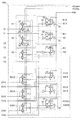
図4は、制御回路30のブロック図である。
FIG. 4 is a block diagram of the
制御回路30は、320行の走査線Y(Y1〜Y320)に対応して、320個の単位制御回路P(P1〜P320)を備える。各単位制御回路Pには、電圧VCOMLと、電圧VCOMHと、電圧VCOMLまたは電圧VCOMHのいずれかを選択する極性制御信号POLと、が供給される。
The
単位制御回路Pは、極性制御信号POLを保持するラッチ回路Qと、極性制御信号POLに応じて電圧VCOMLまたは電圧VCOMHのいずれかを選択的に出力する選択回路Rと、を備える。ラッチ回路Qは、極性制御信号POLを保持する方法から、2つに大別できる。1つは、1行目の走査線Y1に対応して設けられたラッチ回路Q1と、320行目の走査線Y320に対応して設けられたラッチ回路Q320と、である。もう1つは、上述のラッチ回路Q1,Q320を除くラッチ回路Q2〜Q319である。 The unit control circuit P includes a latch circuit Q that holds the polarity control signal POL, and a selection circuit R that selectively outputs either the voltage VCOML or the voltage VCOMH according to the polarity control signal POL. The latch circuit Q can be roughly divided into two types from the method of holding the polarity control signal POL. One is a latch circuit Q1 provided corresponding to the first scanning line Y1, and a latch circuit Q320 provided corresponding to the 320th scanning line Y320. The other is latch circuits Q2 to Q319 excluding the above-described latch circuits Q1 and Q320.
まず、ラッチ回路Q2〜Q319について、以下に説明する。 First, the latch circuits Q2 to Q319 will be described below.
q行目(qは、2≦q≦319を満たす整数)の走査線Yqに対応して設けられたラッチ回路Qqは、否定論理和演算回路(以降、NOR回路と呼ぶ)31と、第1のインバータ32と、第2のインバータ33と、第1のクロックドインバータ34と、第2のクロックドインバータ35と、を備える。
A latch circuit Qq provided corresponding to the scanning line Yq in the q-th row (q is an integer satisfying 2 ≦ q ≦ 319) includes a negative OR operation circuit (hereinafter referred to as a NOR circuit) 31,
NOR回路31の2つの入力端子には、それぞれ、(q−1)行目の走査線Y(q−1)と、(q+1)行目の走査線Y(q+1)と、が接続されている。NOR回路31の出力端子には、第1のインバータ32の入力端子と、第1のクロックドインバータ34の反転入力制御端子と、第2のクロックドインバータ35の非反転入力制御端子と、が接続されている。
The two input terminals of the NOR
第1のインバータ32の出力端子には、第1のクロックドインバータ34の非反転入力制御端子と、第2のクロックドインバータ35の反転入力制御端子と、が接続されている。
The output terminal of the
第1のクロックドインバータ34の入力端子からは、極性制御信号POLが入力される。第1のクロックドインバータ34の出力端子には、第2のインバータ33の入力端子が接続されている。
The polarity control signal POL is input from the input terminal of the first clocked
第2のクロックドインバータ35の入力端子には、第2のインバータ33の出力端子が接続され、第2のクロックドインバータ35の出力端子には、第2のインバータ33の入力端子が接続されている。
The output terminal of the
以上のラッチ回路Qqは、以下のように動作する。 The above latch circuit Qq operates as follows.
すなわち、走査線Y(q−1)と走査線Y(p+1)とのうち少なくともいずれかに第1の選択電圧が供給されると、ラッチ回路Qqが備えるNOR回路31は、Lレベルの信号を出力する。このLレベルの信号は、第1のクロックドインバータ34の反転入力制御端子に入力されるとともに、第1のインバータ32で反転され、Hレベルの信号として第1のクロックドインバータ34の非反転入力端子に入力される。このため、第1のクロックドインバータ34は、オン状態となり、極性制御信号POLを反転して出力する。この第1のクロックドインバータ34から反転して出力された極性制御信号POLは、第2のインバータ33により反転されて選択回路Rに出力される。
That is, when the first selection voltage is supplied to at least one of the scanning line Y (q−1) and the scanning line Y (p + 1), the NOR
以上のように、走査線駆動回路により走査線Y(q−1)と走査線Y(q+1)とのうち少なくともいずれかに第1の選択電圧が供給されると、ラッチ回路Qpは、極性制御信号POLを取り込む。 As described above, when the first selection voltage is supplied to at least one of the scanning line Y (q−1) and the scanning line Y (q + 1) by the scanning line driving circuit, the latch circuit Qp controls the polarity. The signal POL is captured.
一方、走査線Y(q−1)と走査線Y(p+1)との両方に第1の選択電圧が供給されないと、ラッチ回路Qqが備えるNOR回路31は、Hレベルの信号を出力する。このHレベルの信号は、第2のクロックドインバータ35の非反転入力制御端子に入力されるとともに、第1のインバータ32で反転され、Lレベルの信号として第2のクロックドインバータ35の反転入力端子に入力される。このため、第2のクロックドインバータ35は、オン状態となり、第2のインバータ33から出力された極性制御信号POLを反転して出力する。この第2のクロックドインバータ35から反転して出力された極性制御信号POLは、再度、第2のインバータ33により入力される。
On the other hand, when the first selection voltage is not supplied to both the scanning line Y (q−1) and the scanning line Y (p + 1), the NOR
以上のように、走査線駆動回路により走査線Y(q−1)と走査線Y(p+1)との両方に第1の選択電圧が供給されないと、ラッチ回路Qpは、既に取り込んでいる極性制御信号POLを第2のインバータ33および第2のクロックドインバータ35により保持する。
As described above, if the first selection voltage is not supplied to both the scanning line Y (q−1) and the scanning line Y (p + 1) by the scanning line driving circuit, the latch circuit Qp has already taken in the polarity control. The signal POL is held by the
次に、ラッチ回路Q1,Q320について、以下に説明する。 Next, the latch circuits Q1 and Q320 will be described below.
ラッチ回路Q1,Q320は、上述のラッチ回路Qqと比べて、NOR回路31の代わりに、Lレベルの信号を出力する電圧VLLの低電位電源を備える。その他の構成は、上述のラッチ回路Qqと同様である。
Latch circuits Q1 and Q320 include a low-potential power supply of voltage VLL that outputs an L level signal, instead of NOR
これらラッチ回路Q1,Q320は、以下のように動作する。 These latch circuits Q1 and Q320 operate as follows.
すなわち、電圧VLLの低電位電源からは、常にLレベルの信号が出力される。このLレベルの信号は、第1のクロックドインバータ34の反転入力制御端子に入力されるとともに、第1のインバータ32で反転され、Hレベルの信号として第1のクロックドインバータ34の非反転入力制御端子に入力される。このため、第1のクロックドインバータ34は、常にオン状態となり、常に極性制御信号POLを反転して出力する。この第1のクロックドインバータ34から反転して出力された極性制御信号POLは、第2のインバータ33により反転されて選択回路Rに出力される。
That is, an L level signal is always output from the low potential power source of the voltage VLL. This L level signal is input to the inverting input control terminal of the first clocked
以上のように、ラッチ回路Q1,Q320は、常に極性制御信号POLを取り込む。 As described above, the latch circuits Q1 and Q320 always take in the polarity control signal POL.
選択回路Rは、インバータ36と、CMOSトランジスタからなる第1のトランスファゲート37と、CMOSトランジスタからなる第2のトランスファゲート38と、を備える。
The selection circuit R includes an
インバータ36の入力端子には、ラッチ回路Qが備える第2のインバータ33の出力端子が接続され極性制御信号POLが入力される。インバータ36の出力端子には、第1のトランスファゲート37の非反転入力制御端子と、第2のトランスファゲート38の反転入力制御端子と、が接続されている。
The output terminal of the
第1のトランスファゲート37の反転入力制御端子(ゲート端子)には、ラッチ回路Qが備える第2のインバータ33の出力端子が接続され極性制御信号POLが入力される。第1のトランスファゲート37の出力端子(ドレイン端子)には、共通線Zが接続されている。
The output terminal of the
また、奇数行目の走査線Yに対応して設けられた選択回路Rが備える第1のトランスファゲート37の入力端子(ソース端子)からは、電圧VCOMHが入力される。一方、偶数行目の走査線Yに対応して設けられた選択回路Rが備える第1のトランスファゲート37の入力端子からは、電圧VCOMLが入力される。
The voltage VCOMH is input from the input terminal (source terminal) of the
第2のトランスファゲート38の非反転入力制御端子には、ラッチ回路Qが備える第2のインバータ33の出力端子が接続され極性制御信号POLが入力される。第2のトランスファゲート38の出力端子には、共通線Zが接続されている。
The output terminal of the
また、奇数行目の走査線Yに対応して設けられた選択回路Rが備える第2のトランスファゲート38の入力端子からは、電圧VCOMLが入力される。一方、偶数行目の走査線Yに対応して設けられた選択回路Rが備える第2のトランスファゲート38の入力端子からは、電圧VCOMHが入力される。
The voltage VCOML is input from the input terminal of the
以上の選択回路Rは、以下のように動作する。 The above selection circuit R operates as follows.
すなわち、ラッチ回路Qが備える第2のインバータ33からLレベルの極性制御信号POLが出力されると、このLレベルの極性制御信号POLは、第1のトランスファゲート37の反転入力制御端子に入力されるとともに、インバータ36で反転され、Hレベルの極性制御信号POLとして第1のトランスファゲート37の非反転入力制御端子に入力される。このため、第1のトランスファゲート37は、オン状態となる。
That is, when the L level polarity control signal POL is output from the
オン状態となった第1のトランスファゲート37が、奇数行目の走査線Yに対応して設けられた選択回路Rが備えるものであれば、電圧VCOMHを共通線Zに出力する。一方、オン状態となった第1のトランスファゲート37が、偶数行目の走査線Yに対応して設けられた選択回路Rが備えるものであれば、電圧VCOMLを共通線Zに出力する。
If the
一方、ラッチ回路Qが備える第2のインバータ33からHレベルの極性制御信号POLが出力されると、このHレベルの極性制御信号POLは、第2のトランスファゲート38の非反転入力制御端子に入力されるとともに、インバータ36で反転され、Lレベルの極性制御信号POLとして第2のトランスファゲート38の反転入力制御端子に入力される。このため、第2のトランスファゲート38は、オン状態となる。
On the other hand, when the H level polarity control signal POL is output from the
オン状態となった第2のトランスファゲート38が、奇数行目の走査線Yに対応して設けられた選択回路Rが備えるものであれば、電圧VCOMLを共通線Zに出力する。一方、オン状態となった第2のトランスファゲート38が、偶数行目の走査線Yに対応して設けられた選択回路Rが備えるものであれば、電圧VCOMHを共通線Zに出力する。
If the
<第1実施形態の選択回路Rの変形例>
図5は、前記選択回路Rの変形例である選択回路RAのブロック図であり、トランスファゲートに用いるスイッチング素子として単チャネルのスイッチングトランジスタを使用した例を示している。
<Modification of Selection Circuit R of First Embodiment>
FIG. 5 is a block diagram of a selection circuit RA which is a modification of the selection circuit R, and shows an example in which a single channel switching transistor is used as a switching element used for a transfer gate.
選択回路RAは、PchのスイッチングトランジスタからなるPchトランスファゲートRPと、NchのスイッチングトランジスタからなるNchトランスファゲートRNと、を備える。 The selection circuit RA includes a Pch transfer gate RP composed of a Pch switching transistor and an Nch transfer gate RN composed of an Nch switching transistor.
PchトランスファゲートRPの入力端子(ソース端子)には、電圧VCOMHが接続され、PchトランスファゲートRPの制御端子(ゲート端子)には、ラッチ回路Qの出力端子が接続され極性制御信号POLが入力される。PchトランスファゲートRPの出力端子(ドレイン端子)には、共通線Zが接続されている。 The voltage VCOMH is connected to the input terminal (source terminal) of the Pch transfer gate RP, the output terminal of the latch circuit Q is connected to the control terminal (gate terminal) of the Pch transfer gate RP, and the polarity control signal POL is input. The A common line Z is connected to the output terminal (drain terminal) of the Pch transfer gate RP.
PchトランスファゲートRPの入力端子に電圧VCOMHを接続することで、NchトランスファゲートRNの入力端子に電圧VCOMHを接続する場合よりもゲート−ソース間の電圧VGSを大きくすることができるため、動作良好で、更に、低オン抵抗化とオフリークの低減も実現することができる。 By connecting the voltage VCOMH to the input terminal of the Pch transfer gate RP, the gate-source voltage VGS can be made larger than when the voltage VCOMH is connected to the input terminal of the Nch transfer gate RN. In addition, a low on-resistance and a reduction in off-leak can be realized.
NchトランスファゲートRNの入力端子(ソース端子)には、電圧VCOMLが接続され、NchトランスファゲートRNの制御端子(ゲート端子)には、ラッチ回路Qの出力端子が接続され極性制御信号POLが入力される。NchトランスファゲートRNの出力端子(ドレイン端子)には、共通線Zが接続されている。 The voltage VCOML is connected to the input terminal (source terminal) of the Nch transfer gate RN, the output terminal of the latch circuit Q is connected to the control terminal (gate terminal) of the Nch transfer gate RN, and the polarity control signal POL is input. The A common line Z is connected to the output terminal (drain terminal) of the Nch transfer gate RN.
NchトランスファゲートRNの入力端子に電圧VCOMLを接続することで、PchトランスファゲートRPを用いる場合よりもゲート−ソース間の電圧VGSを大きくすることができるため、動作良好で、更に、低オン抵抗化とオフリークの低減も実現することができる。 By connecting the voltage VCOML to the input terminal of the Nch transfer gate RN, the gate-source voltage VGS can be made larger than when the Pch transfer gate RP is used, so that the operation is good and the on-resistance is further reduced. In addition, off-leakage can be reduced.
尚、選択回路RAを用いる場合には、偶数行目の走査線Yに対応して設けられたラッチ回路Qにおいて、第2のインバータ33を削除して、第1のクロックドインバータ34から反転して出力された極性制御信号POLをそのままに出力するように構成することで、共通線Zに電圧VCOMHと電圧VCOMLを交互に出力することができる。
When the selection circuit RA is used, the
以上の選択回路RAは、以下のように動作する。 The above selection circuit RA operates as follows.
すなわち、ラッチ回路QからLレベルの極性制御信号POLが出力されると、このLレベルの極性制御信号POLは、PchトランスファゲートRPの制御端子に入力される。このため、PchトランスファゲートRPは、オン状態となる。オン状態となったPchトランスファゲートRPは、電圧VCOMHを共通線Zに出力する。 That is, when the L level polarity control signal POL is output from the latch circuit Q, the L level polarity control signal POL is input to the control terminal of the Pch transfer gate RP. For this reason, the Pch transfer gate RP is turned on. The Pch transfer gate RP in the on state outputs the voltage VCOMH to the common line Z.
一方、ラッチ回路QからHレベルの極性制御信号POLが出力されると、このHレベルの極性制御信号POLは、NchトランスファゲートRNの制御端子に入力される。このため、NchトランスファゲートRNは、オン状態となる。オン状態となったNchトランスファゲートRNは、電圧VCOMLを共通線Zに出力する。 On the other hand, when the H level polarity control signal POL is output from the latch circuit Q, the H level polarity control signal POL is input to the control terminal of the Nch transfer gate RN. For this reason, the Nch transfer gate RN is turned on. The Nch transfer gate RN in the on state outputs the voltage VCOML to the common line Z.
このように選択回路RAでは、トランスファゲートに用いるスイッチング素子を単チャネル化することにより、前記選択回路Rに用いられているようなCMOSスイッチング素子を用いる場合に比べて回路面積を小さくすることができる。また、高電位の電圧VCOMHにPchのスイッチング素子を接続し、低電位の電圧VCOMLにNchのスイッチング素子を接続する構成とし、夫々を排他的にオンするように構成したことにより、選択回路RAは1本の制御信号のみでの駆動が可能となり、前記選択回路Rのようにインバータ36を用いた反転信号を形成する必要が無いため、インバータ36を削減できる。従って、一層の回路面積の削減を実現することができる。
As described above, in the selection circuit RA, the circuit area can be reduced by using a single channel switching element used for the transfer gate as compared with the case where the CMOS switching element used in the selection circuit R is used. . In addition, the selection circuit RA is configured such that the Pch switching element is connected to the high potential voltage VCOMH and the Nch switching element is connected to the low potential voltage VCOML, and each is turned on exclusively. Driving with only one control signal is possible, and it is not necessary to form an inversion signal using the
尚、電圧VCOMHと電圧VCOMLと、スイッチング素子のゲート電位としてゲート端子に印加する極性制御信号POLの電位関係は、ゲートHigh電圧(極性制御信号POLの高電位)>電圧VCOMH>電圧VCOML>=ゲートLow電圧(極性制御信号POLの低電位)、の関係を満足するように構成する。 The potential relationship between the voltage VCOMH and the voltage VCOML and the polarity control signal POL applied to the gate terminal as the gate potential of the switching element is as follows: gate high voltage (high potential of the polarity control signal POL)> voltage VCOMH> voltage VCOML> = gate The configuration is such that the relationship between the low voltage (low potential of the polarity control signal POL) is satisfied.
このように構成することにより、トランスファゲートに用いるスイッチング素子を単チャネル化しても効率的な低オン抵抗化とスイッチング素子のオフリーク低減を実現することが出来る。 With such a configuration, even if the switching element used for the transfer gate is made into a single channel, it is possible to efficiently reduce the on-resistance and reduce the off-leakage of the switching element.
更に好ましくは、電圧VCOMHと電圧VCOMLと、スイッチング素子のゲート電位としてゲート端子に印加する極性制御信号POLの電位関係を、ゲートHigh電圧>電圧VCOMH−|Pchのトランスファゲートの閾値|>電圧VCOML+|Nchのトランスファゲートの閾値|>=ゲートLow電圧、を満足するように構成することで、各スイッチング素子は閾値以下でオフできるため、オフリークを確実に防止することができる。 More preferably, the potential relationship between the voltage VCOMH and the voltage VCOML and the polarity control signal POL applied to the gate terminal as the gate potential of the switching element is expressed as follows: gate high voltage> voltage VCOMH− | Pch transfer gate threshold value |> voltage VCOML + | By configuring the Nch transfer gate to satisfy the threshold value | >> = the gate low voltage, each switching element can be turned off below the threshold value, so that off-leakage can be reliably prevented.
尚、各電圧の設定は、例えば、ゲートHigh電圧は後述する電圧VGHと同じ8V、ゲートLow電圧は後述する電圧VGLと同じ0V、電圧VCOMHは4V、電圧VCOMLは0Vに設定される。 For example, the gate high voltage is set to 8 V which is the same as the voltage VGH described later, the gate low voltage is set to 0 V which is the same as the voltage VGL described later, the voltage VCOMH is set to 4 V, and the voltage VCOML is set to 0 V.
以上のラッチ回路Qおよび選択回路R(又は選択回路RA)を備えた制御回路30の動作について、図5を用いて説明する。
The operation of the
図6は、走査線駆動回路10および制御回路30のタイミングチャートである。
FIG. 6 is a timing chart of the scanning
時刻t1,t2,・・・は、それぞれ1水平期間を示している。 Times t1, t2,... Each indicate one horizontal period.
まず、時刻t1において、極性制御信号POLを電圧VLLとして、極性制御信号POLをLレベルとする。すると、単位制御回路P1,P320は、常に極性制御信号POLを取り込むラッチ回路Q1,Q320により、Lレベルの極性制御信号POL(選択回路RAを用いる場合は、ラッチ回路Q320により、Hレベルの極性制御信号POL)を取り込んで、選択回路R1,R320により、電圧VCOMHおよび電圧VCOMLをそれぞれ出力する。このため、単位制御回路P1に接続された共通線Z1は、電圧VCOMHとなり、単位制御回路P320に接続された共通線Z320は、電圧VCOMLとなる。 First, at time t1, the polarity control signal POL is set to the voltage VLL, and the polarity control signal POL is set to the L level. Then, the unit control circuits P1 and P320 always use the latch circuits Q1 and Q320 to fetch the polarity control signal POL, and the L level polarity control signal POL (if the selection circuit RA is used, the latch circuit Q320 controls the H level polarity. The signal POL) is taken in, and the voltage VCOMH and the voltage VCOML are output by the selection circuits R1 and R320, respectively. Therefore, the common line Z1 connected to the unit control circuit P1 becomes the voltage VCOMH, and the common line Z320 connected to the unit control circuit P320 becomes the voltage VCOML.
また、電圧VGHは、第1の選択電圧と同じ8Vであり、電圧VGLは、第2の選択電圧と同じ0Vである。 The voltage VGH is 8V, which is the same as the first selection voltage, and the voltage VGL is 0V, which is the same as the second selection voltage.
次に、時刻t2において、走査線駆動回路10から1行目の走査線Y1に第1の選択電圧を供給して、走査線Y1の電圧を電圧VGHとする。すると、走査線Y1に隣接する走査線Y2に対応して設けられた単位制御回路P2は、ラッチ回路Q2により、Lレベルの極性制御信号POL(選択回路RAを用いる場合は、ラッチ回路Q2により、Hレベルの極性制御信号POL)を取り込んで、選択回路R2により、電圧VCOMLを出力する。このため、単位制御回路P2に接続された共通線Z2は、電圧VCOMHから電圧VCOMLに変化する。共通線Z2が4Vから0Vに変化すると、対応する画素電極55の電位は、0Vから−4Vに変化する。このときTFT51のゲートは電圧VGL(0V)であるため、TFT51のドレインからソース、すなわち、画素電極55からデータ線Xにリーク電流が流れてしまう。次に、時刻t3において、走査線駆動回路10から走査線Y1に第1の選択電圧を供給するのを停止して、走査線Y1の電圧を電圧VGLとする。
Next, at time t2, the first selection voltage is supplied from the scanning
同時に、走査線駆動回路10から2行目の走査線Y2に第1の選択電圧を供給して、走査線Y2の電圧を電圧VGHとする。走査線Y2の電位が電圧VGHになることで、データ線駆動回路20から正極性の画像信号が画素電極55に供給される。
At the same time, the first selection voltage is supplied from the scanning
時刻t3で、走査線Y2の電圧が電圧VGHになると、走査線Y2に隣接する走査線Y3に対応して設けられた単位制御回路P3は、ラッチ回路Q3により、Lレベルの極性制御信号POLを取り込んで、選択回路R3により、電圧VCOMHを出力する。このため、単位制御回路P3に接続された共通線Z3は、電圧VCOMHとなる。 When the voltage of the scanning line Y2 becomes the voltage VGH at time t3, the unit control circuit P3 provided corresponding to the scanning line Y3 adjacent to the scanning line Y2 receives the L level polarity control signal POL by the latch circuit Q3. The voltage VCOMH is output by the selection circuit R3. For this reason, the common line Z3 connected to the unit control circuit P3 becomes the voltage VCOMH.
次に、時刻t4において、走査線駆動回路10から走査線Y2に第1の選択電圧を供給するのを停止して、走査線Y2の電圧を電圧VGLとして、対応するTFT51のゲートを0Vとする。このとき画素電極55は正極性の画像信号(0V→4Vの信号)の書き込みにより、例えば、4Vの電位になっているため、画素電極55からデータ線Xへのリーク電流は発生しない。
Next, at time t4, the supply of the first selection voltage from the scanning
走査線Y2の電圧を電圧VGLにするのと同時に、走査線駆動回路10から3行目の走査線Y3に第1の選択電圧を供給して、走査線Y3の電圧を電圧VGHとする。すると、走査線Y3に隣接する走査線Y4に対応して設けられた単位制御回路P4は、ラッチ回路Q4により、Lレベルの極性制御信号POL(選択回路RAを用いる場合は、ラッチ回路Q4により、Hレベルの極性制御信号POL)を取り込んで、選択回路R4により、電圧VCOMLを出力する。このため、単位制御回路P4に接続された共通線Z4は、電圧VCOMLとなる。
Simultaneously with setting the voltage of the scanning line Y2 to the voltage VGL, the first selection voltage is supplied from the scanning
また、走査線Y3に隣接する走査線Y2に対応して設けられた単位制御回路P2は、ラッチ回路Q2により、Lレベルの極性制御信号POLを取り込んで、選択回路R2により、電圧VCOMLを出力する。このため、単位制御回路P2に接続された共通線Z2は、電圧VCOMLとなる。 The unit control circuit P2 provided corresponding to the scanning line Y2 adjacent to the scanning line Y3 takes in the L-level polarity control signal POL by the latch circuit Q2, and outputs the voltage VCOML by the selection circuit R2. . For this reason, the common line Z2 connected to the unit control circuit P2 becomes the voltage VCOML.
次に、時刻t5において、走査線駆動回路10から走査線Y3に第1の選択電圧を供給するのを停止して、走査線Y3の電圧を電圧VGLとする。
Next, at time t5, the supply of the first selection voltage from the scanning
同時に、走査線駆動回路10から4行目の走査線Y4に第1の選択電圧を供給して、走査線Y4の電圧を電圧VGHとする。すると、走査線Y4に隣接する走査線Y5に対応して設けられた単位制御回路P5は、ラッチ回路Q5により、Lレベルの極性制御信号POLを取り込んで、選択回路R5により、電圧VCOMHを出力する。このため、単位制御回路P5に接続された共通線Z5は、電圧VCOMHとなる。
At the same time, the first selection voltage is supplied from the scanning
また、走査線Y4に隣接する走査線Y3に対応して設けられた単位制御回路P3は、ラッチ回路Q3により、Lレベルの極性制御信号POLを取り込んで、選択回路R3により、電圧VCOMHを出力する。このため、単位制御回路P3に接続された共通線Z3は、電圧VCOMHとなる。 The unit control circuit P3 provided corresponding to the scanning line Y3 adjacent to the scanning line Y4 takes in the L level polarity control signal POL by the latch circuit Q3 and outputs the voltage VCOMH by the selection circuit R3. . For this reason, the common line Z3 connected to the unit control circuit P3 becomes the voltage VCOMH.
以降、走査線駆動回路10から奇数行目の走査線Y(ただし、1行目の走査線Y1を除く)に第1の選択電圧を供給すると、時刻t4のように動作し、偶数行目の走査線Y(ただし、320行目の走査線Y320を除く)に第1の選択電圧を供給すると、時刻t5のように動作する。
Thereafter, when the first selection voltage is supplied from the scanning
次に、時刻t7において、走査線駆動回路10から320行目の走査線Y320に第1の選択電圧を供給するのを停止して、走査線Y320の電圧を電圧VGLとする。
Next, at time t7, supply of the first selection voltage from the scanning
同時に、極性制御信号POLを電圧VHHとして、極性制御信号POLをHレベルとする。すると、単位制御回路P1,P320は、常に極性制御信号POLを取り込むラッチ回路Q1,Q320により、Hレベルの極性制御信号POL(選択回路RAを用いる場合は、ラッチ回路Q320により、Lレベルの極性制御信号POL)を取り込んで、選択回路R1,R320により、電圧VCOMLおよび電圧VCOMHをそれぞれ出力する。このため、単位制御回路P1に接続された共通線Z1は、電圧VCOMLとなり、単位制御回路P320に接続された共通線Z320は、電圧VCOMHとなる。 At the same time, the polarity control signal POL is set to the voltage VHH, and the polarity control signal POL is set to the H level. Then, the unit control circuits P1 and P320 always use the latch circuits Q1 and Q320 to take in the polarity control signal POL, and the H level polarity control signal POL (if the selection circuit RA is used, the latch circuit Q320 controls the L level polarity. The signal POL) is taken in, and the voltage VCOML and the voltage VCOMH are output by the selection circuits R1 and R320, respectively. Therefore, the common line Z1 connected to the unit control circuit P1 becomes the voltage VCOML, and the common line Z320 connected to the unit control circuit P320 becomes the voltage VCOMH.
次に、時刻t8において、時刻t2と同様に、走査線駆動回路10から走査線Y1に第1の選択電圧を供給して、走査線Y1の電圧を電圧VGHとする。すると、単位制御回路P2は、電圧VCOMHを出力するので、この単位制御回路P2に接続された共通線Z2は、電圧VCOMHとなる。
Next, at time t8, similarly to time t2, the first selection voltage is supplied from the scanning
次に、時刻t9において、時刻t3と同様に、走査線駆動回路10から走査線Y1に第1の選択電圧を供給するのを停止して、走査線Y1の電圧を電圧VGLとする。
Next, at time t9, similarly to time t3, the supply of the first selection voltage from the scanning
同時に、時刻t3と同様に、走査線駆動回路10から走査線Y2に第1の選択電圧を供給して、走査線Y2の電圧を電圧VGHとする。すると、単位制御回路P3は、電圧VCOMLを出力するので、この単位制御回路P3に接続された共通線Z3は、電圧VCOMLとなる。
At the same time, similarly to time t3, the first selection voltage is supplied from the scanning
次に、時刻t10において、時刻t4と同様に、走査線駆動回路10から走査線Y2に第1の選択電圧を供給するのを停止して、走査線Y2の電圧を電圧VGLとする。
Next, at time t10, similarly to time t4, the supply of the first selection voltage from the scanning
同時に、時刻t4と同様に、走査線駆動回路10から走査線Y3に第1の選択電圧を供給して、走査線Y3の電圧を電圧VGHとする。すると、単位制御回路P4は、電圧VCOMHを出力するので、この単位制御回路P4に接続された共通線Z4は、電圧VCOMHとなる。
At the same time, as at time t4, the first selection voltage is supplied from the scanning
また、時刻t4と同様に、単位制御回路P2は、電圧VCOMHを出力するので、この単位制御回路P2に接続された共通線Z2は、電圧VCOMHとなる。 Similarly to time t4, the unit control circuit P2 outputs the voltage VCOMH, so the common line Z2 connected to the unit control circuit P2 becomes the voltage VCOMH.
次に、時刻t11において、時刻t5と同様に、走査線駆動回路10から走査線Y3に第1の選択電圧を供給するのを停止して、走査線Y3の電圧を電圧VGLとする。
Next, at time t11, similarly to time t5, the supply of the first selection voltage from the scanning
同時に、時刻t5と同様に、走査線駆動回路10から走査線Y4に第1の選択電圧を供給して、走査線Y4の電圧を電圧VGHとする。すると、単位制御回路P5は、電圧VCOMLを出力するので、この単位制御回路P5に接続された共通線Z5は、電圧VCOMLとなる。
At the same time, similarly to time t5, the first selection voltage is supplied from the scanning
また、時刻t5と同様に、単位制御回路P3は、電圧VCOMLを出力するので、この単位制御回路P3に接続された共通線Z3は、電圧VCOMLとなる。 Similarly to time t5, the unit control circuit P3 outputs the voltage VCOML, so the common line Z3 connected to the unit control circuit P3 becomes the voltage VCOML.
以降、走査線駆動回路10から奇数行目の走査線Y(ただし、走査線Y1を除く)に第1の選択電圧を供給すると、時刻t10のように動作し、偶数行目の走査線Y(ただし、走査線Y320を除く)に第1の選択電圧を供給すると、時刻t11のように動作する。
Thereafter, when the first selection voltage is supplied from the scanning
尚、本実施形態では、負電源回路を備えず、走査線Yに供給される第2の選択電圧が0Vであるため、共通線Zが電圧VCOMH(4V)から電圧VCOML(0V)に変位した際に、それに連動して、当該共通線Zに接続された共通電極56と対になった画素電極55の電位が0Vから−4Vに変化すると、当該画素電極55が接続されたTFT51のゲート電位は、0Vであるため、画素電極55からソースにリーク電流が流れてしまうことになる。
In the present embodiment, the negative power supply circuit is not provided, and the second selection voltage supplied to the scanning line Y is 0 V. Therefore, the common line Z is displaced from the voltage VCOMH (4 V) to the voltage VCOML (0 V). In conjunction with this, when the potential of the
しかし、1水平期間後には、当該TFT51のゲートに接続された走査線に第1の選択電圧が1水平期間供給され、正極性の画像信号(0から4Vの電圧)が、データ線駆動回路20から画素電極55に供給される。その後、TFT51このように、リーク電流が流れるのは1水平期間のみであるため、リーク電流による影響が小さい。よって、負電源回路を省略し、正電源回路のみで駆動することができ、回路面積削減またはICの削減や、低消費電力化に貢献することができる。
However, after one horizontal period, the first selection voltage is supplied to the scanning line connected to the gate of the
以上の制御回路30を備えた液晶装置1の動作について、図7、図8を用いて説明する。
The operation of the
図7は、液晶装置1の正極性書込時のタイミングチャートである。図8は、液晶装置1の負極性書込時のタイミングチャートである。
FIG. 7 is a timing chart at the time of positive polarity writing of the
図7、8において、GATE(r)は、320行の走査線Yのうちr行目(rは、1≦r≦320を満たす整数)の走査線Yrの電圧であり、SOURCE(s)は、240列のデータ線Xのうちs列目(sは、1≦s≦240を満たす整数)のデータ線Xsの電圧である。また、PIX(r,s)は、r行目の走査線Yrと、s列目のデータ線Xsと、の交差に対応して設けられたr行s列目の画素50が備える画素電極55の電圧である。また、VCOM(r)は、r行目の共通線Zrに接続された共通電極56の電圧である。
7 and 8, GATE (r) is the voltage of the scanning line Yr of the r-th row (r is an integer satisfying 1 ≦ r ≦ 320) among the 320 scanning lines Y, and SOURCE (s) is , The voltage of the data line Xs of the s-th column (s is an integer satisfying 1 ≦ s ≦ 240) among the 240 data lines X. PIX (r, s) is a
まず、液晶装置1の正極性書込時について、図7を用いて説明する。
First, the positive polarity writing of the
時刻t21において、制御回路30により、共通線Zrに電圧VCOML(0V)を供給する。すると、共通線Zrに接続された共通電極56の電圧VCOM(r)は、電圧VCOMH(4V)から徐々に低下して、時刻t22では、電圧VCOML(0V)となる。
At time t21, the
共通線Zrに接続された共通電極56の電圧VCOM(r)が低下すると、r行s列目の画素50が備える画素電極55の電圧PIX(r,s)は、前記電圧VCOM(r)の低下分(−4V)に応じて電圧VCOM(r)と電圧PIX(r,s)との電位差を保つように低下する。このため、r行s列目の画素50が備える画素電極55の電圧PIX(r,s)は、電圧VP2から徐々に低下して、時刻t22では、電圧VP1((VP2−4)V)となる。よって、この時点で、TFT51のドレインは、画素電極55の負電位、ゲートは、第2の選択電圧の0V、ソースは、電圧VP2になるため、TFT51のドレインからソースにリーク電流が流れてしまう。
When the voltage VCOM (r) of the
しかし、時刻t23において、走査線駆動回路10により、走査線Yrに第1の選択電圧が供給される。すると、走査線Yrの電圧GATE(r)は、上昇して、時刻t24では、電圧VGH(8V)となる。これにより、走査線Yrに接続されたTFT51が全てオン状態となる。したがって、前記リーク電流は流れなくなる。
However, at time t23, the scanning
時刻t25において、データ線駆動回路20により、データ線Xsに正極性の画像信号(0Vから4Vの信号)を供給する。すると、データ線Xsの電圧SOURCE(s)は、徐々に上昇して、時刻t26では、0V以上の電圧VP3となる。 At time t25, the data line driving circuit 20 supplies a positive image signal (a signal from 0V to 4V) to the data line Xs. Then, the voltage SOURCE (s) of the data line Xs gradually increases, and becomes a voltage VP3 of 0 V or more at time t26.
データ線Xsの電圧SOURCE(s)は、正極性の画像信号に基づく画像電圧として、走査線Yrに接続されたオン状態のTFT51を介して、r行s列目の画素50が備える画素電極55に書き込まれる。このため、r行s列目の画素50が備える画素電極55の電圧PIX(r,s)は、徐々に上昇して、時刻t26では、データ線Xsの電圧SOURCE(s)と同電位である電圧VP3となる。
The voltage SOURCE (s) of the data line Xs is an image voltage based on a positive-polarity image signal, and the
時刻t27において、走査線駆動回路10により、走査線Yrに第1の選択電圧を供給するのを停止する。すると、走査線Yrの電圧GATE(r)は、低下して、時刻t28では、電圧VGL(0V)となる。これにより、走査線Yrに接続されたTFT51が全てオフ状態となる。
At time t27, the scanning
このとき、走査線Yrの電圧GATE(r)<画素電極55の電圧VP3であるためドレインからソースへリーク電流は流れない。
At this time, since the voltage GATE (r) of the scanning line Yr <the voltage VP3 of the
次に、液晶装置1の負極性書込時について、図8を用いて説明する。
Next, the negative polarity writing of the
時刻t31において、制御回路30により、共通線Zrに電圧VCOMH(4V)を供給する。すると、共通線Zrに接続された共通電極56の電圧VCOM(r)は、電圧VCOML(0V)から徐々に上昇して、時刻t32では、電圧VCOMH(4V)となる。
At time t31, the
共通線Zrに接続された共通電極56の電圧VCOM(r)が上昇すると、r行s列目の画素50が備える画素電極55の電圧PIX(r,s)は、前記電圧VCOM(r)の上昇分(4V)に応じて電圧VCOM(r)と電圧PIX(r,s)との電位差を保つように上昇する。このため、r行s列目の画素50が備える画素電極55の電圧PIX(r,s)は、徐々に上昇して、時刻t32では、電圧VP5から電圧VP6((VP5+4)V)となる。よって、TFT51のドレインからソースにリーク電流は流れない。
When the voltage VCOM (r) of the
時刻t33において、走査線駆動回路10により、走査線Yrに第1の選択電圧を供給する。すると、走査線Yrの電圧GATE(r)は、上昇して、時刻t34では、電圧VGH(8V)となる。これにより、走査線Yrに接続されたTFT51が全てオン状態となる。
At time t33, the scanning
時刻t35において、データ線駆動回路20により、データ線Xsに負極性の画像信号(4Vから0Vの信号(前記正極性の画像信号の逆極性の信号))を供給する。すると、データ線Xsの電圧SOURCE(s)は、徐々に低下して、時刻t36では、電圧VP4となる。 At time t35, the data line driving circuit 20 supplies a negative polarity image signal (a signal of 4V to 0V (a signal having a polarity opposite to that of the positive polarity image signal)) to the data line Xs. Then, the voltage SOURCE (s) of the data line Xs gradually decreases and becomes the voltage VP4 at time t36.
データ線Xsの電圧SOURCE(s)は、負極性の画像信号に基づく画像電圧として、走査線Yrに接続されたオン状態のTFT51を介して、r行s列目の画素50が備える画素電極55に書き込まれる。このため、r行s列目の画素50が備える画素電極55の電圧PIX(r,s)は、徐々に低下して、時刻t36では、データ線Xsの電圧SOURCE(s)と同電位である電圧VP4となる。
The voltage SOURCE (s) of the data line Xs is an image voltage based on a negative image signal, and the
時刻t37において、走査線駆動回路10により、走査線Yrに第1の選択電圧を供給するのを停止する。すると、走査線Yrの電圧GATE(r)は、低下して、時刻t38では、電圧VGLとなる。これにより、走査線Yrに接続されたTFT51が全てオフ状態となる。
At time t37, the scanning
本実施形態によれば、以下のような効果がある。 According to this embodiment, there are the following effects.
(1)電圧VCOMLを共通線Zに供給して、共通電極56の電圧を電圧VCOMLとした後に、正極性の画像信号をデータ線Xに供給して、正極性の画像電圧を画素電極55に書き込んだ。また、電圧VCOMHを共通線Zに供給して、共通電極56の電圧を電圧VCOMHとした後に、負極性の画像信号をデータ線Xに供給して、負極性の画像電圧を画素電極55に書き込んだ。このため、上述した従来例のように、蓄積容量53と画素容量54との間で電荷が移動しないので、蓄積容量53に特性ばらつきが発生しても、画素電極55の電圧にばらつきが生じない。よって、表示品位の低下を抑制できる。
(1) After supplying the voltage VCOML to the common line Z and setting the voltage of the
(2)共通電極56の電圧VCOM(r)を電圧VCOMLまたは電圧VCOMHに変動させた。したがって、蓄積容量53の一方の電極(補助容量電極57)の電圧を、共通電極56と同様に変動させることができるので、蓄積容量53を画素容量54と一体に形成できる。よって、液晶を挟持する一対の基板として素子基板60および対向基板70のうち素子基板60に、画素容量54を構成する画素電極55および共通電極56を備える液晶装置1により、本発明の液晶装置を構成できる。
(2) The voltage VCOM (r) of the
(3)1水平ラインごとに共通電極56を分割した。そして、電圧VCOMLと電圧VCOMHとを1水平ラインごとに交互に共通電極56に供給するとともに、これら共通電極56の電圧に対応して、正極性の画像信号と、負極性の画像信号とを、1水平ラインごとに交互に各データ線Xに供給した。このため、1フレーム内に正極性書込を行った画素50と負極性書込を行った画素50とを混在させ、これら画素50の間でフリッカを相殺させることができるので、表示品位の低下をさらに抑制できる。
(3) The
(4)制御回路30に、320行の走査線Y(Y1〜Y320)に対応して、320個の単位制御回路P(P1〜P320)を設け、各単位制御回路Pに、ラッチ回路Qおよび選択回路Rを設けた。よって、制御回路30により、電圧VCOMLまたは電圧VCOMHのいずれかを選択的に共通電極56に供給できる。
(4) The
(5)単位制御回路Pに対応する走査線Yに隣接する走査線Yに第1の選択電圧が供給されると、ラッチ回路Qにより、極性制御信号を保持した。このため、複数の単位制御回路Pには、走査線駆動回路10により複数の走査線Yに順次供給される第1の選択電圧に基づいて、極性制御信号が順次保持される。このため、制御回路30は、複数の単位制御回路Pに順次極性制御信号を転送するために、シフトレジスタ回路といった順次転送回路を必要としないので、消費電力を低減できる。
(5) When the first selection voltage is supplied to the scanning line Y adjacent to the scanning line Y corresponding to the unit control circuit P, the latch circuit Q holds the polarity control signal. For this reason, the plurality of unit control circuits P sequentially hold the polarity control signals based on the first selection voltage sequentially supplied to the plurality of scanning lines Y by the scanning
(6)ラッチ回路Q1,Q320により、常に極性制御信号POLを取り込むとともに、ラッチ回路Q2〜Q319により、隣接する2つの走査線Yのうち少なくともいずれかに第1の選択電圧が供給されると、極性制御信号を取り込んだ。このため、走査線駆動回路10により走査線Y1から走査線Y320の順に選択される場合だけでなく、走査線駆動回路10により走査線Y320から走査線Y1の順に選択される場合でも、制御回路30は、複数の単位制御回路Pに順次極性制御信号を転送できる。
(6) When the polarity control signal POL is constantly taken in by the latch circuits Q1 and Q320, and the first selection voltage is supplied to at least one of the two adjacent scanning lines Y by the latch circuits Q2 to Q319, Imported polarity control signal. Therefore, not only when the scanning
(7)本実施形態では、負電源回路を備えず、走査線Yに供給される第2の選択電圧が0Vであるため、共通線Zが電圧VCOMH(4V)から電圧VCOML(0V)に変位した際に、それに連動して、当該共通線Zに接続された共通電極56と対になった画素電極55の電位が0Vから−4Vに変化すると、当該画素電極55が接続されたTFT51のゲート電位は、0Vであるため、画素電極55からソースにリーク電流が流れてしまうことになるが、1水平期間後には、当該TFT51のゲートに接続された走査線に第1の選択電圧が供給され、正極性の画像信号が、データ線駆動回路20から画素電極55に供給される。このように、リーク電流が流れるのは1水平期間のみであるため、リーク電流による影響が小さい。よって、負電源回路を省略し、正電源回路のみで駆動することができ、回路面積削減またはICの削減や、低消費電力化に貢献することができる。
(7) In the present embodiment, since the second selection voltage supplied to the scanning line Y is 0 V without the negative power supply circuit, the common line Z is displaced from the voltage VCOMH (4 V) to the voltage VCOML (0 V). In conjunction with this, when the potential of the
<第2実施形態>
図9は、本発明の第2実施形態に係る制御回路30Aのブロック図である。
Second Embodiment
FIG. 9 is a block diagram of a
本実施形態では、1行目の走査線Y1に対応して設けられたラッチ回路Q1Aと、320行目の走査線Y320に対応して設けられたラッチ回路Q320Aと、の構成が、第1実施形態のラッチ回路Q1,Q320とは異なる。その他の構成については、第1実施形態と同様であり、説明を省略する。 In the present embodiment, the configuration of the latch circuit Q1A provided corresponding to the first scanning line Y1 and the latch circuit Q320A provided corresponding to the 320th scanning line Y320 is the first implementation. Is different from the latch circuits Q1 and Q320. About another structure, it is the same as that of 1st Embodiment, and abbreviate | omits description.
尚、選択回路Rに代えて、選択回路RAを用いることもできる。この場合には、第1実施形態の変形例での説明と同様に、偶数行目の走査線Yに対応して設けられたラッチ回路Qにおいて、第2のインバータ33を削除して、第1のクロックドインバータ34から反転して出力された極性制御信号POLをそのままに出力するように構成することで、共通線Zに電圧VCOMHと電圧VCOMLを交互に出力するように構成するとよい。
In place of the selection circuit R, a selection circuit RA can be used. In this case, as described in the modification of the first embodiment, the
ラッチ回路Q1A,Q320Aは、それぞれ、第1のインバータ32と、第2のインバータ33と、第1のクロックドインバータ34と、第2のクロックドインバータ35と、第3のインバータ39と、を備える。
Each of the latch circuits Q1A and Q320A includes a
ラッチ回路Q1Aが備える第3のインバータ39の入力端子には、走査線Y1が接続され、ラッチ回路Q320Aが備える第3のインバータ39の入力端子には、走査線Y320が接続されている。これら第3のインバータ39の出力端子には、第1のインバータ32の入力端子と、第1のクロックドインバータ34の反転入力制御端子と、第2のクロックドインバータ35の非反転入力制御端子と、が接続されている。
The scanning line Y1 is connected to the input terminal of the
このラッチ回路Q1Aは、以下のように動作する。 The latch circuit Q1A operates as follows.
すなわち、走査線Y1に第1の選択電圧が供給されると、ラッチ回路Q1Aが備える第3のインバータ39は、Lレベルの信号を出力する。このLレベルの信号は、第1のクロックドインバータ34の反転入力制御端子に入力されるとともに、第1のインバータ32で反転され、Hレベルの信号として第1のクロックドインバータ34の非反転入力端子に入力される。このため、第1のクロックドインバータ34は、オン状態となり、極性制御信号POLを反転して出力する。この第1のクロックドインバータ34から反転して出力された極性制御信号POLは、第2のインバータ33により反転されて出力される。
That is, when the first selection voltage is supplied to the scanning line Y1, the
また、ラッチ回路Q320Aは、走査線Y320に第1の選択電圧が供給されると、上述のラッチ回路Q1Aと同様に(ただし、選択回路RAを用いる場合は、第1のクロックドインバータ34から反転して出力された極性制御信号POLをそのまま出力するように)動作する。
Further, when the first selection voltage is supplied to the scanning line Y320, the latch circuit Q320A is inverted from the first clocked
以上のように、走査線駆動回路10により走査線Y1に第1の選択電圧が供給されると、ラッチ回路Q1Aは、極性制御信号POLを取り込み、走査線駆動回路10により走査線Y320に第1の選択電圧が供給されると、ラッチ回路Q320Aは、極性制御信号POLを取り込む。
As described above, when the first selection voltage is supplied to the scanning line Y1 by the scanning
図10は、制御回路30Aのタイミングチャートである。
FIG. 10 is a timing chart of the
図10に示す制御回路30Aのタイミングチャートでは、図6に示した第1実施形態の制御回路30のタイミングチャートと比べて、共通線Z1,Z320の電圧が変動するタイミングが異なる。
The timing chart of the
共通線Z1は、走査線駆動回路10から走査線Y1に第1の選択電圧を供給すると同時に、電圧が反転する。
The common line Z1 supplies the first selection voltage from the scanning
具体的には、時刻t41において、走査線駆動回路10から走査線Y1に第1の選択電圧が供給されると同時に、単位制御回路P1Aは、ラッチ回路Q1Aにより、Lレベルの極性制御信号POLを取り込んで、選択回路R1により、電圧VCOMHを出力する。このため、単位制御回路P1Aに接続された共通線Z1は、電圧VCOMHとなる。また、時刻t44において、走査線駆動回路10から走査線Y1に第1の選択電圧が供給されると同時に、単位制御回路P1Aは、ラッチ回路Q1Aにより、Hレベルの極性制御信号POLを取り込んで、選択回路R1により、電圧VCOMLを出力する。このため、単位制御回路P1Aに接続された共通線Z1は、電圧VCOMLとなる。
Specifically, at time t41, at the same time as the first selection voltage is supplied from the scanning
また、共通線Z320は、共通線Z1と同様に、走査線駆動回路10から走査線Y320に第1の選択電圧が供給されると同時に、電圧の極性が反転する。
Similarly to the common line Z1, the common line Z320 is supplied with the first selection voltage from the scanning
具体的には、時刻t43において、走査線駆動回路10から走査線Y320に第1の選択電圧が供給されると同時に、単位制御回路P320Aは、ラッチ回路Q320Aにより、Lレベルの極性制御信号POL(選択回路RAを用いる場合は、ラッチ回路Q320Aにより、Hレベルの極性制御信号POL)を取り込んで、選択回路R320により、電圧VCOMLを出力する。このため、単位制御回路P320Aに接続された共通線Z320は、電圧VCOMLとなる。
Specifically, at time t43, the first selection voltage is supplied from the scanning
また、時刻t44において、走査線駆動回路10から走査線Y320に第1の選択電圧が供給されると同時に、単位制御回路P320Aは、ラッチ回路Q320Aにより、Hレベルの極性制御信号POLを取り込んで、選択回路R320により、電圧VCOMHを出力する。このため、単位制御回路P320Aに接続された共通線Z320は、電圧VCOMHとなる。
At time t44, the first selection voltage is supplied from the scanning
本実施形態によれば、以下のような効果がある。 According to this embodiment, there are the following effects.
(8)図2に示したように、共通電極56は、1水平ラインごとに分割されている。このため、共通電極56の電圧が隣接する1水平ラインごとに異なると、これらの間で電界が発生して、液晶の配向や秩序が微妙に変化する場合がある。特に、第1実施形態では、図6で示したように、時刻t6〜t7の期間において、共通線Z319の電圧は、電圧VCOMHであり、共通線Z320の電圧は、電圧VCOMLである。ここで、時刻t6〜t7の期間は、走査線駆動回路10により走査線Yを選択する期間の3倍の期間に相当する。このため、時刻t6〜t7の期間において、共通線Z319に接続された共通電極56と、共通線Z320に接続された共通電極56と、の間で電界が発生して、液晶の配向や秩序が大きく変化する場合があった。
(8) As shown in FIG. 2, the
そこで、走査線Y320に第1の選択電圧が供給されると同時に、共通線Z320の電圧の極性を反転させ、共通線Z319の電圧と、共通線Z320の電圧と、が異なる期間を時刻t42〜t43の期間とした。ここで、時刻t42〜t43の期間は、走査線駆動回路10により走査線Yを選択する期間の2倍の期間に相当するので、第1実施形態と比べて、共通線Z319の電圧と、共通線Z320の電圧と、が異なる期間が短い。このため、第1実施形態と比べて、共通線Z319に接続された共通電極56と、共通線Z320に接続された共通電極56と、の間で電界が発生して、液晶の配向や秩序が変化するのを抑制できる。
Therefore, at the same time as the first selection voltage is supplied to the scanning line Y320, the polarity of the voltage of the common line Z320 is inverted, and a period in which the voltage of the common line Z319 and the voltage of the common line Z320 are different is from time t42 to time t42. The period was t43. Here, the period from time t42 to t43 corresponds to a period twice as long as the period for selecting the scanning line Y by the scanning
<第3実施形態>
図11は、本発明の第3実施形態に係る画素50Aの拡大平面図である。
<Third Embodiment>
FIG. 11 is an enlarged plan view of a
本実施形態では、画素50Aが補助共通線ZAおよびコンタクト部58を備える点が、第1実施形態の画素50とは異なる。その他の構成については、第1実施形態と同様であり、説明を省略する。
This embodiment is different from the
補助共通線ZAは、導電性の金属からなり、1水平ラインごとに分割して設けられた共通電極56に対応して設けられている。この補助共通線ZAは、走査線Yに沿って形成されている。
The auxiliary common line ZA is made of a conductive metal and is provided corresponding to the
コンタクト部58は、導電性の金属からなり、領域581において、補助共通線ZAと接続され、領域582において、共通電極56および共通線Zに接続されている。
The
本実施形態によれば、以下のような効果がある。 According to this embodiment, there are the following effects.
(9)1水平ラインごとに分割して設けられた共通電極56に対応して導電性の金属からなる補助共通線ZAを設け、導電性の金属からなるコンタクト部58を介して、共通電極56および共通線Zと、補助共通線ZAと、を接続した。よって、共通電極56および共通線Zの時定数を小さくできる。
(9) An auxiliary common line ZA made of conductive metal is provided corresponding to the
<変形例>
なお、本発明は上述の各実施形態に限定されるものではなく、本発明の目的を達成できる範囲での変形、改良等は本発明に含まれるものである。
<Modification>
Note that the present invention is not limited to the above-described embodiments, and modifications, improvements, and the like within a scope in which the object of the present invention can be achieved are included in the present invention.
例えば、上述の各実施形態では、320行の走査線Yと、240列のデータ線Xと、を備えるものとしたが、これに限らず、例えば、480行の走査線Yと、640列のデータ線Xと、を備えてもよい。 For example, in each of the above-described embodiments, 320 rows of scanning lines Y and 240 columns of data lines X are provided. However, the present invention is not limited to this. For example, 480 rows of scanning lines Y and 640 columns of rows are provided. And a data line X.
また、上述の各実施形態では、透過型の表示を行うものとしたが、これに限らず、例えば、バックライト41からの光を利用する透過型表示と、外光の反射光を利用する反射型表示と、を兼ね備えた半透過反射型の表示を行ってもよい。 In each of the above-described embodiments, the transmissive display is performed. However, the present invention is not limited to this. For example, the transmissive display using light from the backlight 41 and the reflection using reflected light of external light are used. A transflective display having both mold display and display may be performed.
また、上述の各実施形態では、TFTとして低温ポリシリコンからなるTFT51を設けたが、これに限らず、例えばアモルファスシリコンからなるTFTを設けてもよい。
In each of the embodiments described above, the
また、上述の各実施形態では、共通電極56の上に第2絶縁膜64を形成し、この第2絶縁膜64の上に画素電極55を形成したが、これに限らず、例えば、画素電極55の上に第2絶縁膜64を形成し、この第2絶縁膜64の上に共通電極56を形成してもよい。
In each of the above-described embodiments, the second insulating
また、上述の各実施形態では、液晶がFFSモードで動作するものとしたが、これに限らず、例えばIPSモードで動作するものであってもよい。 In each of the above-described embodiments, the liquid crystal operates in the FFS mode. However, the present invention is not limited to this, and the liquid crystal may operate in the IPS mode, for example.
また、上述の各実施形態では、共通電極56を1水平ラインごとに分割して設けたが、これに限らず、例えば、2水平ラインごとや3水平ラインごとに分割して設けてもよい。
In each of the above-described embodiments, the
ここで、例えば、共通電極56を2水平ラインごとに分割して設けた場合には、制御回路30は、電圧VCOMLと電圧VCOMHとを、各共通電極56に接続された2つの共通線Zごとに、交互に供給する。また、データ線駆動回路20は、正極性書込と負極性書込とを、共通電極56に対応する2水平ラインごとに交互に行う。
Here, for example, when the
<応用例>
次に、上述した第1実施形態に係る液晶装置1を適用した電子機器について説明する。
<Application example>
Next, an electronic apparatus to which the
図14は、液晶装置1を適用した携帯電話機の構成を示す斜視図である。携帯電話機3000は、複数の操作ボタン3001およびスクロールボタン3002、ならびに液晶装置1を備える。スクロールボタン3002を操作することによって、液晶装置1に表示される画面がスクロールされる。
FIG. 14 is a perspective view showing a configuration of a mobile phone to which the
なお、液晶装置1が適用される電子機器としては、図14に示すもののほか、パーソナルコンピュータ、情報携帯端末、デジタルスチルカメラ、液晶テレビ、ビューファインダ型、モニタ直視型のビデオテープレコーダ、カーナビゲーション装置、ページャ、電子手帳、電卓、ワードプロセッサ、ワークステーション、テレビ電話、POS端末、タッチパネルを備えた機器などが挙げられる。そして、これらの各種電子機器の表示部として、前述した液晶装置が適用可能である。
As electronic devices to which the
1…液晶装置、10…走査線駆動回路、15…正電源回路、20…データ線駆動回路、30,30A…制御回路、31…NOR回路、32…第1のインバータ、33…第2のインバータ、34…第1のクロックドインバータ、35…第2のクロックドインバータ、36…インバータ、37…第1のトランスファゲート、38…第2のトランスファゲート、39…第3のインバータ、41…バックライト、50…画素、51…TFT、511…ゲート電極、512…ソース電極、513…ドレイン電極、53…補助容量としての蓄積容量、54…画素容量、55…画素電極、55A…スリット、56…共通電極、57…補助容量電極、60…第1基板としての素子基板、62…ゲート絶縁膜、63…第1絶縁膜、64…第2絶縁膜、68,74…ガラス基板、70…第2基板としての対向基板、71…遮光膜、72…カラーフィルタ、3000…電子機器としての携帯電話機、AA…液晶パネル、A…表示領域、E…電界、P…単位制御回路、POL…極性制御信号、Q…ラッチ回路、R,RA…選択回路、RP…Pchトランスファゲート、RN…Nchトランスファゲート、VCOML…第1電圧としての電圧、VCOMH…第2電圧としての電圧、VHH…電圧、VLL…電圧、X…データ線、Y…走査線、Z…共通線、ZA…補助共通線。
DESCRIPTION OF
Claims (3)
液晶を挟んで前記第1基板に対向配置された第2基板と、
前記複数の走査線及び前記複数の共通線に接続され、第1電圧と、当該第1電圧よりも電位の高い第2電圧と、を交互に前記共通線に供給する制御回路と、
水平走査期間ごとに前記複数の走査線から順次選択した前記走査線に対し、前記画素トランジスタをオンする0V以上の第1の選択電圧を供給するとともに、当該水平走査期間の終了時に前記画素トランジスタをオフする0V以上の第2の選択電圧を供給する走査線駆動回路と、
前記画素トランジスタがオンされた際に、前記共通線を介して共通電極に前記第1電圧が供給されていたときは、前記第1電圧よりも電位の高い正極性の画像信号をオンされた前記画素トランジスタに対応する前記データ線に供給し、前記共通電極に前記第2電圧が供給されていたときは、前記第2電圧よりも電位の低い負極性の画像信号を当該データ線に供給するデータ線駆動回路と、を備え、
前記制御回路は、前記共通線それぞれに対応する単位制御回路で構成され、前記単位制御回路は、
前記共通線に対応する前記走査線と隣接する走査線に接続し、前記隣接する走査線に前記第1の選択電圧が検出されたときは、前記第1電圧または前記第2電圧のどちらを出力するかを決める極性制御信号を反転させ、前記隣接する走査線に前記第1の選択電圧が検出されないときは、前記極性制御信号を保持するラッチ回路と、
前記極性制御信号に応じて、前記第1電圧または前記第2電圧のいずれかを前記共通線に出力する選択回路と、
を有し、前記走査線に前記第1の選択電圧が供給されたことを検出すると、次の水平走査期間に選択される前記走査線に対応する前記共通線に対して供給する電圧を反転させ、前記第1電圧が供給されていたときは前記第2電圧を、前記第2電圧が供給されていたときは前記第1電圧を供給する、
液晶装置。 A plurality of scanning lines, a plurality of data lines intersecting the scanning lines, a plurality of common lines parallel to the scanning lines, and a pixel transistor provided corresponding to the intersection of the plurality of scanning lines and the plurality of data lines A first substrate having:
A second substrate disposed opposite to the first substrate across the liquid crystal;
A control circuit connected to the plurality of scanning lines and the plurality of common lines, and alternately supplying a first voltage and a second voltage having a higher potential than the first voltage to the common line;
A first selection voltage of 0 V or higher for turning on the pixel transistor is supplied to the scanning lines sequentially selected from the plurality of scanning lines for each horizontal scanning period, and the pixel transistor is turned on at the end of the horizontal scanning period. A scanning line driving circuit for supplying a second selection voltage of 0 V or more to be turned off;
When the first voltage is supplied to the common electrode through the common line when the pixel transistor is turned on, the positive image signal having a higher potential than the first voltage is turned on. Data that is supplied to the data line corresponding to the pixel transistor and supplies a negative-polarity image signal having a lower potential than the second voltage to the data line when the second voltage is supplied to the common electrode. A line drive circuit,
The control circuit includes unit control circuits corresponding to the common lines, and the unit control circuit includes:
Connected to the scanning line adjacent to the scanning line corresponding to the common line, and outputs the first voltage or the second voltage when the first selection voltage is detected on the adjacent scanning line A latch circuit that holds the polarity control signal when the polarity control signal for deciding whether to invert and when the first selection voltage is not detected on the adjacent scanning line;
A selection circuit that outputs either the first voltage or the second voltage to the common line in response to the polarity control signal;
And detecting that the first selection voltage is supplied to the scanning line, the voltage supplied to the common line corresponding to the scanning line selected in the next horizontal scanning period is inverted. The second voltage is supplied when the first voltage is supplied, and the first voltage is supplied when the second voltage is supplied.
Liquid crystal device.
Priority Applications (1)
| Application Number | Priority Date | Filing Date | Title |
|---|---|---|---|
| JP2007171634A JP5224735B2 (en) | 2006-07-03 | 2007-06-29 | Liquid crystal device and electronic device |
Applications Claiming Priority (3)
| Application Number | Priority Date | Filing Date | Title |
|---|---|---|---|
| JP2006183051 | 2006-07-03 | ||
| JP2006183051 | 2006-07-03 | ||
| JP2007171634A JP5224735B2 (en) | 2006-07-03 | 2007-06-29 | Liquid crystal device and electronic device |
Publications (2)
| Publication Number | Publication Date |
|---|---|
| JP2008033298A JP2008033298A (en) | 2008-02-14 |
| JP5224735B2 true JP5224735B2 (en) | 2013-07-03 |
Family
ID=39122721
Family Applications (1)
| Application Number | Title | Priority Date | Filing Date |
|---|---|---|---|
| JP2007171634A Expired - Fee Related JP5224735B2 (en) | 2006-07-03 | 2007-06-29 | Liquid crystal device and electronic device |
Country Status (1)
| Country | Link |
|---|---|
| JP (1) | JP5224735B2 (en) |
Families Citing this family (2)
| Publication number | Priority date | Publication date | Assignee | Title |
|---|---|---|---|---|
| US8081178B2 (en) | 2007-07-10 | 2011-12-20 | Sony Corporation | Electro-optical device, driving circuit, and electronic apparatus |
| WO2013002228A1 (en) * | 2011-06-30 | 2013-01-03 | シャープ株式会社 | Shift register, display drive circuit, display panel, and display device |
Family Cites Families (4)
| Publication number | Priority date | Publication date | Assignee | Title |
|---|---|---|---|---|
| JP2002221941A (en) * | 2001-01-25 | 2002-08-09 | Hitachi Ltd | Liquid crystal display and image display device using the same |
| KR100652215B1 (en) * | 2003-06-27 | 2006-11-30 | 엘지.필립스 엘시디 주식회사 | Liquid crystal display device |
| JP2005300948A (en) * | 2004-04-13 | 2005-10-27 | Hitachi Displays Ltd | Display device and driving method therefor |
| JP2006078920A (en) * | 2004-09-13 | 2006-03-23 | Sony Corp | Display apparatus and driving method for same |
-
2007
- 2007-06-29 JP JP2007171634A patent/JP5224735B2/en not_active Expired - Fee Related
Also Published As
| Publication number | Publication date |
|---|---|
| JP2008033298A (en) | 2008-02-14 |
Similar Documents
| Publication | Publication Date | Title |
|---|---|---|
| JP4241850B2 (en) | Liquid crystal device, driving method of liquid crystal device, and electronic apparatus | |
| KR100968720B1 (en) | Liquid crystal device and electronic apparatus | |
| JP4415393B2 (en) | Driving circuit, liquid crystal device, electronic apparatus, and driving method of liquid crystal device | |
| JP4277894B2 (en) | Electro-optical device, drive circuit, and electronic device | |
| JP4420080B2 (en) | Scanning line driving circuit, electro-optical device, and electronic apparatus | |
| TW200919435A (en) | Electro-optical device, driving circuit, and electronic apparatus | |
| JP4241858B2 (en) | Liquid crystal device and electronic device | |
| US20070229431A1 (en) | Display panel and method of driving display panel using inversion driving method | |
| WO2012133281A1 (en) | Display device | |
| JP4957169B2 (en) | Electro-optical device, scanning line driving circuit, and electronic apparatus | |
| JP2009020213A (en) | Electro-optical device, drive circuit and electronic device | |
| JP5224735B2 (en) | Liquid crystal device and electronic device | |
| JP5046230B2 (en) | Liquid crystal device and electronic device | |
| JP2011013420A (en) | Electro-optical device, method for driving the same, and electronic apparatus | |
| JP4428401B2 (en) | Electro-optical device, drive circuit, and electronic device | |
| JP2009223173A (en) | Electro-optical device, driving circuit, and electronic device | |
| JP2008076733A (en) | Electro-optical device and electronic equipment | |
| JP4811445B2 (en) | Electro-optical device, drive circuit, and electronic device | |
| JP2008096699A (en) | Electro-optic device, method for driving electro-optic device and electronic equipment | |
| JP2009223174A (en) | Electro-optical device, driving circuit, and electronic device | |
| JP2008015399A (en) | Electro-optical device, driving circuit and electronic apparatus | |
| JP2009003068A (en) | Electro-optic device, driving method for it, and electronic apparatus | |
| JP2009216805A (en) | Electro-optical device, driving circuit, and electronic equipment |
Legal Events
| Date | Code | Title | Description |
|---|---|---|---|
| A621 | Written request for application examination |
Free format text: JAPANESE INTERMEDIATE CODE: A621 Effective date: 20091224 |
|
| A711 | Notification of change in applicant |
Free format text: JAPANESE INTERMEDIATE CODE: A711 Effective date: 20100526 |
|
| RD02 | Notification of acceptance of power of attorney |
Free format text: JAPANESE INTERMEDIATE CODE: A7422 Effective date: 20100526 |
|
| A521 | Written amendment |
Free format text: JAPANESE INTERMEDIATE CODE: A523 Effective date: 20100630 |
|
| A131 | Notification of reasons for refusal |
Free format text: JAPANESE INTERMEDIATE CODE: A131 Effective date: 20120214 |
|
| A711 | Notification of change in applicant |
Free format text: JAPANESE INTERMEDIATE CODE: A711 Effective date: 20120330 |
|
| A521 | Written amendment |
Free format text: JAPANESE INTERMEDIATE CODE: A523 Effective date: 20120409 |
|
| A131 | Notification of reasons for refusal |
Free format text: JAPANESE INTERMEDIATE CODE: A131 Effective date: 20120703 |
|
| A521 | Written amendment |
Free format text: JAPANESE INTERMEDIATE CODE: A523 Effective date: 20120828 |
|
| TRDD | Decision of grant or rejection written | ||
| A01 | Written decision to grant a patent or to grant a registration (utility model) |
Free format text: JAPANESE INTERMEDIATE CODE: A01 Effective date: 20130219 |
|
| A61 | First payment of annual fees (during grant procedure) |
Free format text: JAPANESE INTERMEDIATE CODE: A61 Effective date: 20130312 |
|
| R150 | Certificate of patent or registration of utility model |
Ref document number: 5224735 Country of ref document: JP Free format text: JAPANESE INTERMEDIATE CODE: R150 Free format text: JAPANESE INTERMEDIATE CODE: R150 |
|
| FPAY | Renewal fee payment (event date is renewal date of database) |
Free format text: PAYMENT UNTIL: 20160322 Year of fee payment: 3 |
|
| R250 | Receipt of annual fees |
Free format text: JAPANESE INTERMEDIATE CODE: R250 |
|
| R250 | Receipt of annual fees |
Free format text: JAPANESE INTERMEDIATE CODE: R250 |
|
| R250 | Receipt of annual fees |
Free format text: JAPANESE INTERMEDIATE CODE: R250 |
|
| R250 | Receipt of annual fees |
Free format text: JAPANESE INTERMEDIATE CODE: R250 |
|
| R250 | Receipt of annual fees |
Free format text: JAPANESE INTERMEDIATE CODE: R250 |
|
| LAPS | Cancellation because of no payment of annual fees |