JP5219364B2 - Time interval adjustment type differential capacitance sensor device - Google Patents
Time interval adjustment type differential capacitance sensor device Download PDFInfo
- Publication number
- JP5219364B2 JP5219364B2 JP2006345902A JP2006345902A JP5219364B2 JP 5219364 B2 JP5219364 B2 JP 5219364B2 JP 2006345902 A JP2006345902 A JP 2006345902A JP 2006345902 A JP2006345902 A JP 2006345902A JP 5219364 B2 JP5219364 B2 JP 5219364B2
- Authority
- JP
- Japan
- Prior art keywords
- circuit
- detector
- drive
- adjustment circuit
- drive signal
- Prior art date
- Legal status (The legal status is an assumption and is not a legal conclusion. Google has not performed a legal analysis and makes no representation as to the accuracy of the status listed.)
- Expired - Fee Related
Links
Images


Classifications
-
- G—PHYSICS
- G01—MEASURING; TESTING
- G01D—MEASURING NOT SPECIALLY ADAPTED FOR A SPECIFIC VARIABLE; ARRANGEMENTS FOR MEASURING TWO OR MORE VARIABLES NOT COVERED IN A SINGLE OTHER SUBCLASS; TARIFF METERING APPARATUS; MEASURING OR TESTING NOT OTHERWISE PROVIDED FOR
- G01D5/00—Mechanical means for transferring the output of a sensing member; Means for converting the output of a sensing member to another variable where the form or nature of the sensing member does not constrain the means for converting; Transducers not specially adapted for a specific variable
- G01D5/12—Mechanical means for transferring the output of a sensing member; Means for converting the output of a sensing member to another variable where the form or nature of the sensing member does not constrain the means for converting; Transducers not specially adapted for a specific variable using electric or magnetic means
- G01D5/14—Mechanical means for transferring the output of a sensing member; Means for converting the output of a sensing member to another variable where the form or nature of the sensing member does not constrain the means for converting; Transducers not specially adapted for a specific variable using electric or magnetic means influencing the magnitude of a current or voltage
- G01D5/24—Mechanical means for transferring the output of a sensing member; Means for converting the output of a sensing member to another variable where the form or nature of the sensing member does not constrain the means for converting; Transducers not specially adapted for a specific variable using electric or magnetic means influencing the magnitude of a current or voltage by varying capacitance
Description
本発明は、差動容量センサ装置及び方法に関し、特に、零変位における容量検知回路のヌル・バイアス調整(零位偏倚調整:null bias trimming)に関する。 The present invention relates to a differential capacitance sensor device and method, and more particularly to null bias adjustment (zero bias adjustment) of a capacitance detection circuit at zero displacement.
差動容量センサ・デバイスは、一般に周知である。近年の加速度計、圧力変換器、及び同様の変換器は、差動容量システムを採用して、検知エレメント、例えば、検査質量(proof-mass)又はダイアフラムのヌル位置又は運動を、基本的な機械−電気変換原理にしたがって検出することが多い。これは、特に、差動容量が利用されている微小電気機械システム(MEMS)センサ・デバイスに当てはまる。差動容量を検出して検知エレメントのヌル・バイアス又は運動を検出するセンサ・デバイスの生産において、コストを押し上げる主要な要因となっているのは、零変位においてヌル・バイアスとなるように容量性検知システムを調整する必要があることである。 Differential capacitive sensor devices are generally well known. Modern accelerometers, pressure transducers, and similar transducers employ a differential capacitive system to detect the null position or motion of sensing elements, such as proof-mass or diaphragms, basic machinery. -It is often detected according to the principle of electrical conversion. This is especially true for microelectromechanical system (MEMS) sensor devices where differential capacitance is utilized. In the production of sensor devices that detect differential capacitance to detect the sensing element's null bias or motion, the major factor driving the cost is the capacitive nature of null displacement at zero displacement. It is necessary to adjust the detection system.
既存の差動容量検出駆動回路は、通常、逆極性、即ち、「ミラー的(対称的:mirrored)励起信号を差動センサの一対のコンデンサに印加する。全てのものが等しいとすると、これにより、一対のコンデンサ間の共通接続点において、ヌル信号(零位)が生成し、トランスインピーダンス増幅器の入力となる。実際のセンサでは、ミラー的励起信号は、一対のコンデンサのヌル・バイアスにおいて、共通接続点にてヌル信号の偏倚が生ずる。何故なら、回路を完全に均衡にすることはできず、コンデンサ対を形成する2つの感知コンデンサを全く同一にすることはできないからである。このため、従来の回路は、従前よりフロント・エンド偏倚調整を導入して、プログラム可能コンデンサ・アレイを追加することにより、ヌル・バイアスにおいてヌル信号を生成するようにしている。 Existing differential capacitance sensing drive circuits typically apply a reverse polarity, or “mirrored” excitation signal, to a pair of capacitors in a differential sensor. A null signal (zero) is generated at the common connection point between a pair of capacitors and becomes the input of a transimpedance amplifier.In actual sensors, the mirror excitation signal is common at the null bias of a pair of capacitors. A null signal bias occurs at the connection point because the circuit cannot be perfectly balanced and the two sensing capacitors forming the capacitor pair cannot be exactly the same. Traditional circuits have previously introduced a front end bias adjustment and added a programmable capacitor array to eliminate null bias. And so as to generate null signals.
これらの追加のコンデンサ・アレイは、種々の構成において応用することができる。例えば、既存の差動容量検出器駆動回路は、通常、並列バイアス調整アレイ又は駆動レベル・バイアス調整アレイのいずれかを利用して、容量性検知システムを調整して零変位においてヌル・バイアスとなるようにしている。 These additional capacitor arrays can be applied in various configurations. For example, existing differential capacitance detector drive circuits typically use either a parallel bias adjustment array or a drive level bias adjustment array to adjust the capacitive sensing system to null bias at zero displacement I am doing so.
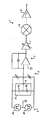
図1は、既存の検出器駆動回路1の典型的な並列構成の一例を示す。駆動回路1は、一対の駆動信号発生器2a及び2bを有する駆動部2を備えており、駆動信号発生器2a及び2bは、逆極性即ち「ミラー的」励起信号を、差動容量センサ3の2つの感知コンデンサ3a及び3bに印加するような構造となっている。回路の均衡が完全に取れており、しかも2つの感知コンデンサ3a、3bが全く同一であれば、これらのミラー的励起信号の印加によって、零変位において、コンデンサ対3a、3b間の共通接続点4にてヌル電位となり、トランスインピーダンス増幅器5への入力となる。しかしながら、実際の差動容量センサでは、コンデンサ対3a、3bの零変位において、信号は共通接続点4では偏倚しており、ヌル電位ではない。このため、プログラマブル・コンデンサ・アレイ6によってフロント・エンド・バイアス調整を導入して、ヌル信号を生成している。
FIG. 1 shows an example of a typical parallel configuration of an existing detector driving circuit 1. The drive circuit 1 includes a drive unit 2 having a pair of
バイアス調整コンデンサ・アレイ6を切り換えて、2つの感知コンデンサ3a又は3bの内小さい方と並列となるように、回路1に加えると、大きい方との差が得られる。このとき、零変位においてコンデンサ対3a、3b間の共通接続点4にて生成するヌル信号を、トランスインピーダンス増幅器5に入力する。トランスインピーダンス増幅器5の出力は、可変利得増幅器7の入力となり、増幅した信号を同期復調器8に出力する。同期復調器8の出力は、フィルタ・バッファ9によりフィルタリングされる。
When the bias adjustment capacitor array 6 is switched and added to the circuit 1 so as to be in parallel with the smaller one of the two sensing capacitors 3a or 3b, a difference from the larger one is obtained. At this time, a null signal generated at the
図2は、検出器駆動回路1の別の共通構成を示し、バイアス調整コンデンサ・アレイ6を切り換えて、駆動部2が出力する励起駆動信号の経路に加入し、印加された励起電圧、つまり、コンデンサ対3a、3bのその側からの有効信号を優先的に低減する。 FIG. 2 shows another common configuration of the detector driving circuit 1, which switches the bias adjusting capacitor array 6 to join the path of the excitation driving signal output by the driving unit 2, and applies the applied excitation voltage, that is, The effective signal from that side of the capacitor pair 3a, 3b is preferentially reduced.
このようなプログラマブルなバイアス調整コンデンサ・アレイ6によるフロント・エンド・バイアス調整は、従来技術によって教示されているように、コスト高で、しかも適正に実現するのが困難である。図示のように、典型的な手法では複雑な回路が必要となり、個別形態で実現するのが困難であり、特定用途の集積回路に多大な投資が必要となるのが通常である。
したがって、典型的な技術的現状における、MEMS加速度計、圧力変換器、及びその他の変換デバイスにおける差動容量検出器駆動回路の均衡化に対する、これら及びその他の制約を克服するデバイス及び方法が望まれている。
Such front-end bias adjustment with the programmable bias adjustment capacitor array 6 is costly and difficult to implement properly, as taught by the prior art. As shown in the figure, a typical technique requires a complicated circuit, is difficult to realize in an individual form, and usually requires a large investment in a specific application integrated circuit.
Accordingly, devices and methods are desired that overcome these and other constraints on the balancing of differential capacitance detector drive circuits in MEMS accelerometers, pressure transducers, and other conversion devices in a typical technical state of the art. ing.
本発明は、差動容量変換器の動作のための装置及び方法であり、一対の駆動信号発生器の動作により、実質的に逆極性の励起駆動信号を発生すること、励起駆動信号を差動容量センサの一対の感知コンデンサに印加すること、一対の感知コンデンサ間にある共通接続点において差動容量を検知すること、ならびに共通接続点において感知コンデンサ対のヌル・バイアスを調整するために駆動信号発生器を個別に制御することを含む。 The present invention is an apparatus and method for the operation of a differential capacitance converter, wherein an excitation drive signal having substantially opposite polarity is generated by the operation of a pair of drive signal generators, and the excitation drive signal is differentially generated. Driving signal to apply to a pair of sensing capacitors of a capacitance sensor, to sense differential capacitance at a common connection point between the pair of sensing capacitors, and to adjust the null bias of the sensing capacitor pair at the common connection point Including individually controlling the generator.
本発明の装置及び方法は、逆極性の励起駆動信号のタイミングを個別に指令することによって、従前からの切換バイアス調整コンデンサ・アレイの複雑さ及び高コストを解消する。この個別指令により、2つの励起駆動信号の一方を他方に比較して、しかるべき時間間隔だけ広げ、2つの励起駆動信号が正確に対称的ではなくなるようする。長い方の駆動間隔が事実上有効な励起駆動信号を増大させ、これに比例して、広い方、即ち、期間が長い方の駆動側のセンサ容量の重み(significance)が増す。このように、従来技術の検出器駆動回路の高価な切換バイアス調整コンデンサ・アレイを用いずに、ヌル・バイアスを調整する。更に、励起駆動信号の個別指令を、単純なデジタル・コントローラを用いて制御する。励起駆動信号を発生する信号発生器を、周波数が高い方のクロック発振器の分周のために設ける場合、駆動励起信号の時間幅は、クロックの時間刻み幅(1周期)ずつ個別に調節することができ、これによって、調整可能性比がクロック刻み幅対駆動幅の比率と同等となる。 The apparatus and method of the present invention eliminates the complexity and high cost of traditional switched bias adjustment capacitor arrays by individually commanding the timing of reverse polarity excitation drive signals. This individual command causes one of the two excitation drive signals to be compared to the other and spread by an appropriate time interval so that the two excitation drive signals are not exactly symmetrical. The longer drive interval effectively increases the effective excitation drive signal, and in proportion to this, the sensor capacitance weight on the wider side, i.e. the longer side, is increased. Thus, the null bias is adjusted without using the expensive switched bias adjustment capacitor array of the prior art detector driver circuit. Furthermore, the individual commands of the excitation drive signal are controlled using a simple digital controller. When a signal generator for generating an excitation drive signal is provided for frequency division of the clock oscillator having the higher frequency, the time width of the drive excitation signal should be adjusted individually for each time interval (one period) of the clock. This allows the adjustability ratio to be equal to the ratio of clock step to drive width.
例えば、4MHzの基準クロックを用いて、50%デューティ・サイクルで、40KHz励起駆動信号を駆動する場合、クロックの時間刻み幅は励起信号の1%となる。励起信号の一方の幅を、1クロック刻み幅だけ変化させると、元の差動容量不均衡が1%調整されることになる。クロック・レート対駆動比を高くすることによって、直接的にバイアス調整分解能を高くすることができる。
本発明の一態様によれば、調整刻み幅が駆動サイクル毎に一定とならないようにジッタを追加し、分解能を更に高めることができる。
For example, when a 40 KHz excitation drive signal is driven with a 50 MHz duty cycle using a 4 MHz reference clock, the time interval of the clock is 1% of the excitation signal. Changing the width of one of the excitation signals by one clock step will adjust the original differential capacitance imbalance by 1%. By increasing the clock rate to drive ratio, the bias adjustment resolution can be directly increased.
According to one embodiment of the present invention, jitter can be added so that the adjustment step size does not become constant for each driving cycle, and the resolution can be further improved.
本発明の別の態様によれば、同じデジタル・コントローラを用いて倍率を調整することにより、バイアス零位を調整する。限定ではなく一例として、倍率調整回路は、同期復調器へのゲート・スイッチの時間を増分し、スイッチのデューティ・サイクルに比例する、信号の一部だけを通過させる。スイッチの「オン」時間を制御することにより、積分器/フィルタに流す全信号の割合を制御する。 According to another aspect of the invention, the bias zero is adjusted by adjusting the magnification using the same digital controller. By way of example and not limitation, the scaling circuit increments the time of the gate switch to the synchronous demodulator and passes only a portion of the signal that is proportional to the duty cycle of the switch. By controlling the “on” time of the switch, the proportion of the total signal that flows to the integrator / filter is controlled.
本発明の別の態様によれば、同じデジタル・コントローラを用い、温度センサから入力を供給することによって、バイアス零位調整及び倍率調整機能の一方又は双方に温度補償を行う。デジタル・コントローラは、温度センサからの入力の関数として、可変刻み幅を供給するようにプログラムされている。 According to another aspect of the present invention, temperature compensation is performed for one or both of the bias zero adjustment function and the magnification adjustment function by using the same digital controller and supplying an input from the temperature sensor. The digital controller is programmed to provide a variable step size as a function of the input from the temperature sensor.
図面において、同様の番号は同様の要素を示すものとする。
図面は、新規のヌル・バイアス調整を行う、差動容量変換デバイスを動作させる検出器駆動回路のための、本発明の装置及び方法を示す。
In the drawings, like numerals indicate like elements.
The drawings show the apparatus and method of the present invention for a detector driver circuit operating a differential capacitance conversion device with a novel null bias adjustment.
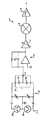
図3は、検出器駆動回路10として具体化した本発明のヌル・バイアス調整装置及び方法を、限定ではなく一例として示す模式図である。本発明の検出器駆動回路10は、一対の駆動信号発生器12a及び12bを有する駆動回路12を含み、信号発生器12a及び12bは、差動容量センサ14の2つの異なる感知コンデンサ14a及び14bに、実質的に逆極性の励起駆動信号を印加するような構造となっている。コンデンサ対14a、14b間の共通接続点16が、トランスインピーダンス増幅器18に結合されている。トランスインピーダンス増幅器18の出力は、同期復調器20を介して結合されており、同期復調器20の出力は、フィルタ・バッファ22によってフィルタリングされる。
FIG. 3 is a schematic diagram illustrating, by way of example and not limitation, the null bias adjustment apparatus and method of the present invention embodied as the detector drive circuit 10. The detector drive circuit 10 of the present invention includes a drive circuit 12 having a pair of
駆動回路12の一対の信号発生器12a及び12bが発生する励起駆動信号は、高周波システム・クロック発振器24の分周のために供給される。一対のスイッチ26a及び26bは、異なる駆動信号発生器12a及び12bを個別に制御する。既知の形式のプログラマブル・デジタル・コントローラ28は、個々のスイッチ26a、26bを制御し、スイッチ26a、26bによって、信号発生器12a、12b、及びこれらが発生する励起駆動信号を個々に制御する。励起駆動信号は、信号発生器12a、12bによって、励起周波数で発生されるが、システム・クロック発振器24のクロック周波数の方が遥かに高く、励起周波数はその端数(fraction)である。
The excitation drive signals generated by the pair of
本発明によれば、デジタル・コントローラ28によって回路30をプログラムすることによって、センサ励起信号を発生し、ヌル・バイアス調整機能を設けるためのスイッチ26a、26bの動作タイミングを与える。例えば、デジタル・コントローラ28は、従来のPICプロセッサ又はプログラマブル・ロジック・アレイであり、その出力線32が駆動信号発生器12a、12bに接続されている。デジタル・コントローラ28は、個別に駆動信号発生器12a、12b、したがって逆極性の励起駆動信号のタイミングを指令することにより、検知エレメント(図示せず)の零変位において、コンデンサ対14a、14bの間の共通接続点16にて測定したときに、ヌル・バイアスが実質的に零となるようにする。このように、通常高価な従来技術の切換バイアス調整コンデンサ・アレイ6がなくても、共通接続点16におけるヌル・バイアスを調整することができる。
In accordance with the present invention, the circuit 30 is programmed by the
オプションの選択肢として、デジタル・コントローラ28によって倍率調整機能回路(scale factor trim function circuit)34を設ける。つまり、別のコントローラ出力線36を通じて、デジタル・コントローラ28は、同期復調器20に供給する信号を制御するゲート・スイッチ38に指令を送る。倍率調整機能回路34は、同期復調器のスイッチ38の「オン」時間を制御する。一方、スイッチの「オン」時間を制御することにより、復調器20及びフィルタ22に達する全信号の割合(%)を制御する。例えば、倍率調整機能回路34は、差動容量センサ14からの出力信号の一部のみを通すために、同期復調器20への同期復調器ゲート・スイッチ38の時間を増分する。同期復調器スイッチ38によって通過が許された信号の部分は、スイッチ38のデューティ・サイクルに比例する。このように、「オン」時間を制御して、復調器20及びフィルタ22まで達することが許される全信号の割合を決定することにより、同じデジタル・コントローラ28によってデバイスの倍率を調整し、デバイスのヌル・バイアス調整を行う。
As an optional option, a scale factor
図4は、本発明にしたがって、デジタル・コントローラ28が個々に制御する機能として、2つの駆動信号発生器12a、12bが出力する励起駆動信号に対するヌル・バイアス調整機能の効果を示す。これによって、デジタル・コントローラ28のヌル・バイアス調整回路30は、逆極性の励起駆動信号のタイミングを個別に指令する。このように励起駆動信号のタイミングを個別に指令することによって、2つの駆動信号発生器の一方12a(又は12b)が出力する励起駆動信号を、2つの駆動信号発生器の他方12b(又は12a)が出力する他方の励起駆動信号に対して、しかるべき調整時間間隔(i1)だけ広げることができ、2つの励起駆動信号が、従来技術においてそうであるように、完全な対称とはならないようにする。つまり、2つの駆動信号発生器の一方12a(又は12b)が出力する初期励起駆動信号40は、2つの駆動信号発生器の他方12b(又は12a)が出力する逆極性の励起駆動信号42のミラー・イメージ(mirror image)であり、これによって、双方の励起駆動信号40及び42は実質的に同じ時間長(t0)を有することになる。本発明によれば、デジタル・コントローラ28のヌル・バイアス調整回路30は、2つの駆動信号発生器の一方12a(又は12b)のタイミングを個別に指令して、励起駆動信号44を発生し、te=t0+i1にしたがって、初期信号長(t0)を、しかるべき調整時間間隔(i1)だけ長くして、延長信号長(te)とする。ここで、調整時間間隔(i1)は、システム・クロック24の1つ以上の時間刻み幅(i)である。
FIG. 4 illustrates the effect of the null bias adjustment function on the excitation drive signals output by the two
駆動時間間隔(to)が長い程、有効励起駆動信号が事実上大きくなり、これに比例して、広い方、即ち、期間が長い方の駆動側のセンサ容量の重み(significance)が増す。したがって、従来技術では通常である高価な切換偏倚調整アレイがなくても、ヌル・バイアスを調整する。更に、図3に示す形式の回路10にしたがって、単純なデジタル・コントローラ28を用いて、個々の励起駆動信号を制御する。2つの駆動信号発生器12a、12bは、励起信号の周波数よりも高いクロック発振器24の周波数を分周するために設けられている。したがって、回路10を用いて、周波数が高い方のクロック24の時間刻み幅ずつ、個々の駆動励起信号間隔t0及びteの幅を調節することができる。周波数が高い方のクロック24の1つ以上の時間刻み幅(i)の単位で個々の駆動励起時間間隔t0及びteの幅を調節することにより、調整可能率(trimmability ratio)が、クロック刻み幅対駆動幅の比率と同等となる。これを以下の例によって実証する。
The longer the drive time interval (t o ), the greater the effective excitation drive signal, and proportionally the sensor capacitance weight on the drive side that is wider, that is, the longer is increased. Therefore, the null bias is adjusted without the expensive switching bias adjustment array that is normal in the prior art. Further, individual excitation drive signals are controlled using a simple
一例として、システム・クロック発振器24を4MHz基準クロックに選択し、デューティ・サイクルが50パーセントである、40KHz励起駆動信号を駆動するために用いる。この例では、クロック時間刻み幅は、駆動励起時間間隔t0の1パーセントである。したがって、励起信号の一方の幅を、クロック刻み幅1つだけ変化させることにより、初期の差動容量不均衡が1パーセントだけ調整される。バイアス調整分解能を高めるには、クロック・レート対駆動比を高めることによって直接得られる。あるいは、第2バイアス調整段を追加することによって、ジッタを駆動励起時間間隔teに追加して、偏倚調整の分解能を高め、2つの時間間隔状態の間で駆動が断片的に交代するようにする。これによって、有効バイアス調整は、2つの状態間で、いずれかの状態において費やした時間の端数に直接比例することになる。この端数駆動技法は、基準クロック刻み幅の他に、数種類の大きさ(several orders magnitude)の調整分解能を容易に得ることができる。 As an example, the system clock oscillator 24 is selected to be a 4 MHz reference clock and used to drive a 40 KHz excitation drive signal having a 50% duty cycle. In this example, the clock time step size is 1% of the driving excitation time interval t 0. Thus, changing the width of one of the excitation signals by one clock step will adjust the initial differential capacitance imbalance by 1 percent. Increasing the bias adjustment resolution is directly obtained by increasing the clock rate versus drive ratio. Alternatively, by adding a second bias adjustment stage, adding jitter to drive the excitation time interval t e, increase the resolution of the bias adjustment, so that the drive between the two time intervals state is fragmentarily Substitution To do. This makes the effective bias adjustment directly proportional to the fraction of time spent in either state between the two states. This fractional driving technique can easily obtain adjustment resolutions of several orders magnitude in addition to the reference clock step size.
選択肢として、コントローラ28が、電源投入時に、名目クロック−駆動「スキュー」(nominal clock-to-drive skew)に固定する。その後、デジタル・コントローラのヌル・バイアス調整回路30が、精細なバイアス調節スイッチとして、個々のスイッチ26a、26bを制御する。
As an option, the
これらの微細調整のバイアス調節スイッチ26a、26bは、検出駆動回路10の温度補償としても機能する。また、本発明のヌル・バイアス調整方法は、システム温度センサ46(図3に示す)からの入力の関数として、可変量の時間刻み幅(i)を提供するようにデジタル・プロセス・コントローラ28をプログラムすれば、非常に低コストの温度補償方法としても機能する。システム温度センサ46は、システム温度を表す温度信号(T)を出力するような構造となっている。デジタル・コントローラのヌル・バイアス調整回路30は、可変時間刻み幅(i)を個々のスイッチ26a、26bの一方又は双方に印加し、ヌル・バイアス調整を、システム温度の関数として制御するようにプログラムされている。任意選択肢として、可変時間刻み幅(i)を同期復調器ゲート・スイッチ38に印加して、調整の倍率を、システム温度の関数として制御するように、デジタル・コントローラの倍率調整機能回路34をプログラムすることもできる。
These fine adjustment bias adjustment switches 26 a and 26 b also function as temperature compensation for the detection drive circuit 10. The null bias adjustment method of the present invention also allows the
任意選択肢として、デジタル・コントローラのヌル・バイアス調整回路30によって、ジッタを駆動信号に追加し、バイアス調整刻み幅i1が駆動サイクル毎に一定ではないようにする。このジッタ導入による多様化(inconsistency)は、分解能を高めることになるが、低周波側波帯が混入することが予想され、用途によってはこの低周波側波帯をフィルタリングする必要がある場合もある。 Optionally, the digital controller's null bias adjustment circuit 30 adds jitter to the drive signal so that the bias adjustment step size i 1 is not constant from drive cycle to drive cycle. This inconsistency due to the introduction of jitter will increase the resolution, but it is expected that low frequency sidebands will be mixed, and depending on the application, it may be necessary to filter the low frequency sidebands. .
以上、本発明の好適な実施形態について図示し説明したが、発明の技術的思想及び範囲から逸脱することなく、種々の変更が可能であることは認められるであろう。 While the preferred embodiment of the invention has been illustrated and described, it will be appreciated that various changes can be made without departing from the spirit and scope of the invention.
Claims (10)
一対の感知コンデンサ(14a、14b)と、
前記感知コンデンサ(14a、14b)のそれぞれに、実質的に逆極性の励起駆動信号をそれぞれ印加するよう構成された一対の駆動信号発生器(12a、12b)と、
前記駆動信号発生器(12a、12b)のそれぞれを個別に制御するヌル・バイアス調整回路(30)及びスイッチ(38)を制御する倍率調整回路(34)を含むプロセスコントローラ(28)と、
前記一対の感知コンデンサ(14a、14b)の間の共通接合点(16)に結合されているトランスインピーダンス増幅器(18)と、
前記トランスインピーダンス増幅器(18)の出力に結合されている同期復調器(20)と、
前記同期復調器(20)の出力に結合されているフィルタ・バッファ(22)と
を備え、前記スイッチ(38)は前記トランスインピーダンス増幅器(18)の出力と前記同期復調器(20)との間に結合され、前記ヌル・バイアス調整回路(30)は前記一対の感知コンデンサ(14a、14b)のヌル・バイアスを調整し、前記倍率調整回路(34)は前記スイッチ(38)の「オン」時間を制御することにより前記変換器のデバイス倍率を調整することを特徴とする検出器駆動回路。 A detector drive circuit (10) for operation of the differential capacitance converter comprising:
A pair of sensing capacitors (14a, 14b);
A pair of drive signal generators (12a, 12b) configured to apply a substantially opposite polarity excitation drive signal to each of the sensing capacitors (14a, 14b);
A process controller (28) including a null bias adjustment circuit (30) for individually controlling each of the drive signal generators (12a, 12b) and a magnification adjustment circuit (34) for controlling the switch (38);
A transimpedance amplifier (18) coupled to a common junction (16) between the pair of sensing capacitors (14a, 14b);
A synchronous demodulator (20) coupled to the output of the transimpedance amplifier (18);
And a filter buffer (22) coupled to the output of the synchronous demodulator (20), the switch (38) between the output of the transimpedance amplifier (18) and the synchronous demodulator (20). And the null bias adjustment circuit (30) adjusts the null bias of the pair of sensing capacitors (14a, 14b), and the magnification adjustment circuit (34) sets the “on” time of the switch (38). A detector driving circuit for adjusting a device magnification of the converter by controlling
システム温度を表す温度信号を前記倍率調整回路(34)に出力するように結合されている温度センサ(46)を備えており、
前記倍率調整回路(34)は更に、前記温度信号の関数として前記スイッチ(38)を可変制御するよう構成されていることを特徴とする検出器駆動回路。 The detector drive circuit (10) of claim 1, further comprising:
A temperature sensor (46) coupled to output a temperature signal representative of system temperature to the magnification adjustment circuit (34);
The detector drive circuit, wherein the magnification adjustment circuit (34) is further configured to variably control the switch (38) as a function of the temperature signal.
高周波システム・クロック発振器と、
前記第1及び第2駆動信号発生器のそれぞれを制御するよう接続されている第1及び第2スイッチ(26a、26b)と
をさらに備え、
前記ヌル・バイアス調整回路(30)は前記第1及び第2スイッチ(26a、26b)を個別に制御するよう接続されていることを特徴とする検出器駆動回路。 The detector drive circuit (10) of claim 1, further comprising a system clock oscillator (24), wherein the pair of sensing capacitors (14a, 14b) is a common connection point (16). The pair of drive signal generators are provided for frequency division of the system clock oscillator (24) and are substantially opposite in polarity to the first and second sense capacitors coupled to the first and second sense capacitors. First and second drive signal generators (12a, 12b) configured to generate a second excitation drive signal, respectively, wherein the first and second drive signal generators (12a, 12b) Each of the first and second excitation drive signals is connected to be applied to each of the first and second sensing capacitors (14a, 14b) of the differential capacitance converter;
High frequency system clock oscillator,
First and second switches (26a, 26b) connected to control each of the first and second drive signal generators;
The detector drive circuit, wherein the null bias adjustment circuit (30) is connected to control the first and second switches (26a, 26b) individually.
Applications Claiming Priority (2)
| Application Number | Priority Date | Filing Date | Title |
|---|---|---|---|
| US11/317,383 US7368923B2 (en) | 2005-12-22 | 2005-12-22 | Time interval trimmed differential capacitance sensor |
| US11/317,383 | 2005-12-22 |
Publications (3)
| Publication Number | Publication Date |
|---|---|
| JP2007171203A JP2007171203A (en) | 2007-07-05 |
| JP2007171203A5 JP2007171203A5 (en) | 2009-09-17 |
| JP5219364B2 true JP5219364B2 (en) | 2013-06-26 |
Family
ID=38192881
Family Applications (1)
| Application Number | Title | Priority Date | Filing Date |
|---|---|---|---|
| JP2006345902A Expired - Fee Related JP5219364B2 (en) | 2005-12-22 | 2006-12-22 | Time interval adjustment type differential capacitance sensor device |
Country Status (3)
| Country | Link |
|---|---|
| US (1) | US7368923B2 (en) |
| EP (1) | EP1855096A3 (en) |
| JP (1) | JP5219364B2 (en) |
Cited By (2)
| Publication number | Priority date | Publication date | Assignee | Title |
|---|---|---|---|---|
| JP2015135245A (en) * | 2014-01-16 | 2015-07-27 | セイコーエプソン株式会社 | Physical quantity detection circuit, physical quantity detection device, electronic apparatus, and moving body |
| JP2016109465A (en) * | 2014-12-02 | 2016-06-20 | 株式会社堀場エステック | Electrical capacitance sensor |
Families Citing this family (11)
| Publication number | Priority date | Publication date | Assignee | Title |
|---|---|---|---|---|
| EP1959562B1 (en) * | 2007-02-15 | 2010-12-08 | STMicroelectronics Srl | Fully differential demodulator with variable gain and method for demodulating a signal |
| DE102007048402A1 (en) * | 2007-10-09 | 2009-04-16 | Gerd Reime | Control unit and method for triggering a function |
| DE102009000950A1 (en) | 2009-02-02 | 2010-08-05 | Robert Bosch Gmbh | Component with a micromechanical microphone structure and method for operating such a microphone component |
| EP2473901A1 (en) | 2009-09-03 | 2012-07-11 | Koninklijke Philips Electronics N.V. | Touch sensing output device |
| JP2011193978A (en) * | 2010-03-18 | 2011-10-06 | Canon Inc | Apparatus and method for driving capacitive electromechanical transduction apparatus |
| WO2011154468A1 (en) | 2010-06-08 | 2011-12-15 | Iee International Electronics & Engineering S.A. | Robust capacitive measurement system |
| US9551738B2 (en) * | 2010-06-08 | 2017-01-24 | Iee International Electronics & Engineering S.A. | Robust capacitive measurement system |
| DE102012210004B4 (en) | 2012-06-14 | 2014-11-06 | Robert Bosch Gmbh | Bar detector with control circuit |
| US20150268268A1 (en) * | 2013-06-17 | 2015-09-24 | Freescale Semiconductor, Inc. | Inertial sensor with trim capacitance and method of trimming offset |
| US10006930B2 (en) * | 2014-06-03 | 2018-06-26 | Northrop Grumman Systems Corporation | Performance optimization of a differential capacitance based motion sensor |
| EP3495826B1 (en) * | 2017-12-07 | 2020-11-25 | EM Microelectronic-Marin SA | Electronic device for measuring a physical parameter |
Family Cites Families (29)
| Publication number | Priority date | Publication date | Assignee | Title |
|---|---|---|---|---|
| JP2675861B2 (en) * | 1988-07-01 | 1997-11-12 | キヤノン株式会社 | Recording method and apparatus |
| US4890598A (en) * | 1988-07-29 | 1990-01-02 | Nu-Tech Industries, Inc. | High efficiency blower |
| US4896100A (en) * | 1988-08-30 | 1990-01-23 | Hitec Products, Inc. | Signal conditioner for capacitive transducer |
| US4987779A (en) * | 1989-02-28 | 1991-01-29 | United Technologies Corporation | Pulse-driven accelerometer arrangement |
| FR2656698B1 (en) * | 1989-12-29 | 1992-05-07 | Vectavib | DEVICE FOR MEASURING VARIATIONS IN THE CAPACITY OF A CAPACITOR FORMING, IN PARTICULAR, A SENSOR. |
| JPH05322921A (en) * | 1992-05-19 | 1993-12-07 | Hitachi Ltd | Acceleration sensor and air bag system using the same |
| US5367217A (en) * | 1992-11-18 | 1994-11-22 | Alliedsignal Inc. | Four bar resonating force transducer |
| US5450762A (en) * | 1992-12-17 | 1995-09-19 | Alliedsignal Inc. | Reactionless single beam vibrating force sensor |
| US5456111A (en) * | 1994-01-24 | 1995-10-10 | Alliedsignal Inc. | Capacitive drive vibrating beam accelerometer |
| JPH07325102A (en) * | 1994-06-02 | 1995-12-12 | Canon Inc | Angular velocity indicator |
| JPH0862247A (en) * | 1994-08-23 | 1996-03-08 | Hitachi Ltd | Acceleration sensor and its manufacturing method |
| JP3139305B2 (en) * | 1994-08-24 | 2001-02-26 | 株式会社村田製作所 | Capacitive acceleration sensor |
| JP3322067B2 (en) * | 1995-04-24 | 2002-09-09 | 株式会社デンソー | Physical quantity detector |
| GB2301671B (en) * | 1995-05-30 | 1999-10-13 | Allied Signal Inc | Angular rate sensor electronic balance |
| US5682788A (en) * | 1995-07-12 | 1997-11-04 | Netzer; Yishay | Differential windshield capacitive moisture sensor |
| JP3435979B2 (en) * | 1996-04-26 | 2003-08-11 | 株式会社デンソー | Physical quantity detector |
| US5744968A (en) * | 1996-04-30 | 1998-04-28 | Motorola Inc. | Ratiometric circuit |
| US5831164A (en) | 1997-01-21 | 1998-11-03 | Conrad Technologies, Inc. | Linear and rotational accelerometer |
| JPH11258092A (en) * | 1998-03-13 | 1999-09-24 | Omron Corp | Physical quantity measuring device |
| US6269698B1 (en) * | 1999-03-25 | 2001-08-07 | Alliedsignal Inc. | Vibrating beam force sensor |
| JP3588276B2 (en) * | 1999-07-26 | 2004-11-10 | 株式会社山武 | Sensor signal processing circuit |
| JP4327395B2 (en) * | 1999-08-31 | 2009-09-09 | アナログ デバイセス インコーポレーテッド | Sensors and micromachined equipment |
| US6731121B1 (en) | 1999-10-15 | 2004-05-04 | Microsensors Corp. | Highly configurable capacitive transducer interface circuit |
| JP4870889B2 (en) * | 1999-10-15 | 2012-02-08 | アプロレーザ ディベロップメント カンパニー リミテッド ライアビリティー カンパニー | Highly configurable capacitive transducer interface circuit |
| US6366099B1 (en) * | 1999-12-21 | 2002-04-02 | Conrad Technologies, Inc. | Differential capacitance sampler |
| JP4553084B2 (en) * | 2000-12-11 | 2010-09-29 | 株式会社豊田中央研究所 | Physical quantity detection circuit |
| JP2004361388A (en) * | 2003-05-15 | 2004-12-24 | Mitsubishi Electric Corp | Capacitive type inertial force detection device |
| JP2004364366A (en) * | 2003-06-02 | 2004-12-24 | Seiko Epson Corp | Pwm control system |
| EP1548409A1 (en) * | 2003-12-23 | 2005-06-29 | Dialog Semiconductor GmbH | Differential capacitance measurement |
-
2005
- 2005-12-22 US US11/317,383 patent/US7368923B2/en active Active
-
2006
- 2006-12-20 EP EP06126597A patent/EP1855096A3/en not_active Withdrawn
- 2006-12-22 JP JP2006345902A patent/JP5219364B2/en not_active Expired - Fee Related
Cited By (2)
| Publication number | Priority date | Publication date | Assignee | Title |
|---|---|---|---|---|
| JP2015135245A (en) * | 2014-01-16 | 2015-07-27 | セイコーエプソン株式会社 | Physical quantity detection circuit, physical quantity detection device, electronic apparatus, and moving body |
| JP2016109465A (en) * | 2014-12-02 | 2016-06-20 | 株式会社堀場エステック | Electrical capacitance sensor |
Also Published As
| Publication number | Publication date |
|---|---|
| US7368923B2 (en) | 2008-05-06 |
| EP1855096A3 (en) | 2008-08-20 |
| US20070146019A1 (en) | 2007-06-28 |
| EP1855096A2 (en) | 2007-11-14 |
| JP2007171203A (en) | 2007-07-05 |
Similar Documents
| Publication | Publication Date | Title |
|---|---|---|
| JP5219364B2 (en) | Time interval adjustment type differential capacitance sensor device | |
| WO2010150736A1 (en) | Angular velocity sensor, and synchronous detection circuit used therein | |
| JP3932661B2 (en) | Angular velocity sensor drive circuit | |
| JP2007171203A5 (en) | ||
| JP4310571B2 (en) | Capacitance detection type vibration gyro and capacitance change detection method | |
| JP5458462B2 (en) | Vibration type inertial force detection sensor | |
| JP2006220454A (en) | Sensor circuit for capacitance type physical quantity sensor | |
| JP4561528B2 (en) | Sensor circuit | |
| JP2001333583A (en) | Vibrator driver | |
| JP2018028473A5 (en) | ||
| JP5104936B2 (en) | Acceleration and angular velocity detection device | |
| JP3123174B2 (en) | Sensor signal extraction circuit | |
| JP2006329637A (en) | Angular velocity detector | |
| US9513309B2 (en) | Inertia sensor with switching elements | |
| JP4075152B2 (en) | Angular velocity sensor | |
| IT201900000989A1 (en) | CIRCUIT FOR DETECTING AN ANALOG SIGNAL GENERATED BY A CORRESPONDING SENSOR, ELECTRONIC SYSTEM AND PROCEDURE | |
| JP5187836B2 (en) | Sensor sensitivity adjusting means and sensor manufacturing method | |
| JP2004198310A (en) | Control method of accelerometer | |
| JP2006010408A (en) | Vibratory gyro | |
| JP4631537B2 (en) | Sensor circuit of capacitive physical quantity sensor | |
| JP4406863B2 (en) | Vibration type angular velocity sensor device | |
| JP2014149229A (en) | Angular velocity sensor | |
| JP4935300B2 (en) | Sensor circuit with abnormality detection circuit for self-diagnosis | |
| JP2007093233A (en) | Angular velocity signal processing circuit | |
| KR100270768B1 (en) | Turing angle speed sensor. |
Legal Events
| Date | Code | Title | Description |
|---|---|---|---|
| A521 | Request for written amendment filed |
Free format text: JAPANESE INTERMEDIATE CODE: A523 Effective date: 20090804 |
|
| A621 | Written request for application examination |
Free format text: JAPANESE INTERMEDIATE CODE: A621 Effective date: 20090804 |
|
| RD04 | Notification of resignation of power of attorney |
Free format text: JAPANESE INTERMEDIATE CODE: A7424 Effective date: 20110913 |
|
| A977 | Report on retrieval |
Free format text: JAPANESE INTERMEDIATE CODE: A971007 Effective date: 20111109 |
|
| A131 | Notification of reasons for refusal |
Free format text: JAPANESE INTERMEDIATE CODE: A131 Effective date: 20111115 |
|
| A601 | Written request for extension of time |
Free format text: JAPANESE INTERMEDIATE CODE: A601 Effective date: 20120215 |
|
| A602 | Written permission of extension of time |
Free format text: JAPANESE INTERMEDIATE CODE: A602 Effective date: 20120220 |
|
| A521 | Request for written amendment filed |
Free format text: JAPANESE INTERMEDIATE CODE: A523 Effective date: 20120307 |
|
| A131 | Notification of reasons for refusal |
Free format text: JAPANESE INTERMEDIATE CODE: A131 Effective date: 20120803 |
|
| A521 | Request for written amendment filed |
Free format text: JAPANESE INTERMEDIATE CODE: A523 Effective date: 20121015 |
|
| TRDD | Decision of grant or rejection written | ||
| A01 | Written decision to grant a patent or to grant a registration (utility model) |
Free format text: JAPANESE INTERMEDIATE CODE: A01 Effective date: 20130204 |
|
| A61 | First payment of annual fees (during grant procedure) |
Free format text: JAPANESE INTERMEDIATE CODE: A61 Effective date: 20130305 |
|
| FPAY | Renewal fee payment (event date is renewal date of database) |
Free format text: PAYMENT UNTIL: 20160315 Year of fee payment: 3 |
|
| R150 | Certificate of patent or registration of utility model |
Free format text: JAPANESE INTERMEDIATE CODE: R150 |
|
| R250 | Receipt of annual fees |
Free format text: JAPANESE INTERMEDIATE CODE: R250 |
|
| R250 | Receipt of annual fees |
Free format text: JAPANESE INTERMEDIATE CODE: R250 |
|
| LAPS | Cancellation because of no payment of annual fees |