JP5218219B2 - Manufacturing method of multilayer ceramic electronic component - Google Patents
Manufacturing method of multilayer ceramic electronic component Download PDFInfo
- Publication number
- JP5218219B2 JP5218219B2 JP2009086588A JP2009086588A JP5218219B2 JP 5218219 B2 JP5218219 B2 JP 5218219B2 JP 2009086588 A JP2009086588 A JP 2009086588A JP 2009086588 A JP2009086588 A JP 2009086588A JP 5218219 B2 JP5218219 B2 JP 5218219B2
- Authority
- JP
- Japan
- Prior art keywords
- rod
- laminate
- groove
- forming
- electronic component
- Prior art date
- Legal status (The legal status is an assumption and is not a legal conclusion. Google has not performed a legal analysis and makes no representation as to the accuracy of the status listed.)
- Active
Links
Images

Landscapes
- Ceramic Capacitors (AREA)
- Fixed Capacitors And Capacitor Manufacturing Machines (AREA)
Description
本発明は、たとえば積層セラミックコンデンサなどの積層セラミック電子部品の製造方法に関する。 The present invention relates to a method for manufacturing a multilayer ceramic electronic component such as a multilayer ceramic capacitor.
たとえば積層セラミックコンデンサなどの積層セラミック電子部品の製造方法としては、たとえば、グリーンシートと内部パターンを積層してシート積層体を形成し、これを焼成し、焼成された積層体を切断することによって棒状の積層体を形成し、棒状の積層体に外部電極を導電ペースト塗布等によって形成し、棒状の積層体をさらに切断して個片にする製造方法が知られている(特許文献1および特許文献2等を参照)。
For example, as a method of manufacturing a multilayer ceramic electronic component such as a multilayer ceramic capacitor, for example, a green laminate and an internal pattern are laminated to form a sheet laminate, which is fired, and the fired laminate is cut into a rod shape There is known a manufacturing method in which a laminated body is formed, an external electrode is formed on a rod-shaped laminated body by applying a conductive paste, and the rod-shaped laminated body is further cut into pieces (
しかし、従来技術に係る製造方法では、一つの棒状の積層体ごとに導電ペーストを塗布等することによって外部電極を形成しているため、外部電極の形成に手間がかかり、生産効率に問題がある。 However, in the manufacturing method according to the prior art, since the external electrode is formed by applying a conductive paste to each bar-shaped laminated body, it takes time to form the external electrode, and there is a problem in production efficiency. .
本発明は、このような実状に鑑みてなされ、その目的は、生産効率を改善した積層セラミック電子部品の製造方法を提供することである。 The present invention has been made in view of such a situation, and an object thereof is to provide a method of manufacturing a multilayer ceramic electronic component with improved production efficiency.
上記目的を達成するために、本発明の積層セラミック電子部品の製造方法は、
焼成後に内部電極層となる内部電極パターンと、焼成後にセラミック層となるグリーンシートとが積層してあるシート積層体を準備する工程と、
前記シート積層体を焼成および切断することによって、前記内部電極層が露出する切断面と、前記シート積層体の積層方向に略垂直な側面とを有しており、長手方向に細長い複数の棒状積層体を形成する工程と、
前記複数の棒状積層体を再配列し、前記複数の棒状積層体の前記側面が互いに密着しており、前記複数の棒状積層体の前記切断面が略同一の平面に沿って配置された積層体集合体を形成する工程と、
前記積層体集合体を構成する前記棒状積層体の一部を切除し、前記棒状積層体の前記切断面に溝部を形成する工程と、
前記積層体集合体における前記複数の棒状積層体の前記切断面に外部電極を薄膜形成する工程と、
前記棒状積層体を個片状に切断する工程と、を有する。
In order to achieve the above object, a method for producing a multilayer ceramic electronic component of the present invention comprises:
Preparing a sheet laminate in which an internal electrode pattern that becomes an internal electrode layer after firing and a green sheet that becomes a ceramic layer after firing are laminated;
By firing and cutting the sheet laminate, a plurality of rod-like laminates having a cut surface from which the internal electrode layer is exposed and a side surface substantially perpendicular to the stacking direction of the sheet laminate are elongated in the longitudinal direction. Forming a body;
The laminated body in which the plurality of rod-like laminated bodies are rearranged, the side surfaces of the plurality of rod-like laminated bodies are in close contact with each other, and the cut surfaces of the plurality of rod-like laminated bodies are arranged along substantially the same plane. Forming an aggregate;
Cutting a part of the rod-like laminate constituting the laminate aggregate and forming a groove in the cut surface of the rod-like laminate; and
Forming a thin film of external electrodes on the cut surfaces of the plurality of rod-like laminates in the laminate assembly; and
Cutting the rod-shaped laminate into individual pieces.
本発明に係る積層セラミック電子部品の製造方法では、複数の棒状積層体を再配列した積層体集合体を形成することによって、複数の棒状積層体に対して同時に外部電極を薄膜形成することができる。複数の棒状積層体に対して一度に外部電極の形成ができるため、本発明に係る製造方法は生産効率が良い。また、側面を密着させることによって、外部電極を構成する材料が棒状積層体の側面に回り込むことを防止できる。また、棒状積層体の切断面に溝部を形成することによって、形成される外部電極の面積を増加させることができる。本発明に係る積層セラミック電子部品の製造方法によって得られた電子部品は、外部電極の面積が広いため、高い実装強度を有する。 In the method for manufacturing a multilayer ceramic electronic component according to the present invention, it is possible to simultaneously form a thin film of external electrodes on a plurality of rod-like laminates by forming a laminate assembly in which a plurality of rod-like laminates are rearranged. . Since external electrodes can be formed at a time for a plurality of rod-shaped laminates, the production method according to the present invention has good production efficiency. Moreover, it can prevent that the material which comprises an external electrode wraps around the side surface of a rod-shaped laminated body by sticking a side surface. Moreover, the area of the external electrode to be formed can be increased by forming the groove in the cut surface of the rod-shaped laminate. The electronic component obtained by the method for manufacturing a multilayer ceramic electronic component according to the present invention has a high mounting strength because the area of the external electrode is large.
また、本発明に係る積層電子部品の製造方法では、前記溝部の形状を制御する工程をさらに有していてもよく、これによって製造される電子部品の実装強度等を調整または制御することができる。 Moreover, in the method for manufacturing a laminated electronic component according to the present invention, the method may further include a step of controlling the shape of the groove, and the mounting strength and the like of the electronic component manufactured thereby can be adjusted or controlled. .
また、例えば、前記溝部を形成する工程において、前記溝部は、前記積層体集合体における前記複数の棒状積層体の長手方向に略直交する方向に延在するように形成されてもよい。また、前記溝部を形成する工程において、略V字状の前記溝部を形成してもよい。 Further, for example, in the step of forming the groove portion, the groove portion may be formed so as to extend in a direction substantially orthogonal to a longitudinal direction of the plurality of rod-shaped stacked bodies in the stacked body aggregate. Further, in the step of forming the groove portion, the substantially V-shaped groove portion may be formed.
また、例えば、本発明に係る積層電子部品の製造方法では、前記棒状積層体を個片状に切断する工程において、前記積層体集合体を構成する前記複数の棒状積層体を、前記溝部に沿って切断してもよい。これによって、切断時または切断後における電子部品の角部欠けおよび割れ等を防止することができる。また、前記溝部に沿って切断することにより、切断時の位置精度を向上させることができる。 Further, for example, in the method for manufacturing a laminated electronic component according to the present invention, in the step of cutting the rod-like laminate into individual pieces, the plurality of rod-like laminates constituting the laminate assembly are arranged along the groove portions. May be cut. As a result, it is possible to prevent chipping and cracking of the electronic component during or after cutting. Moreover, the position accuracy at the time of a cutting | disconnection can be improved by cut | disconnecting along the said groove part.
また、本発明に係る積層電子部品の製造方法では、前記シート積層体の表面を平滑化する工程をさらに有してもよい。これにより、棒状積層体の側面が平滑化されるため、外部電極を薄膜形成する際に、外部電極を構成する材料が棒状積層体の側面に回り込むことを効果的に防止できる。 Moreover, in the manufacturing method of the multilayer electronic component which concerns on this invention, you may further have the process of smoothing the surface of the said sheet | seat laminated body. Thereby, since the side surface of the rod-shaped laminated body is smoothed, when forming the thin film of the external electrode, it is possible to effectively prevent the material constituting the external electrode from wrapping around the side surface of the rod-shaped laminated body.
本発明の第2の観点に係る積層電子部品の製造方法では、
焼成後に内部電極層となる内部電極パターンと、焼成後にセラミック層となるグリーンシートとが積層してあるシート積層体を準備する工程と、
前記シート積層体の一部を切除し、前記シート積層体の表面に溝部を形成する工程と、
前記シート積層体を焼成および前記溝部に沿って切断することによって、前記内部電極層が露出する切断面と、前記シート積層体の積層方向に略垂直な側面とを有しており、長手方向に細長い複数の棒状積層体を形成する工程と、
前記複数の棒状積層体を再配列し、前記複数の棒状積層体の前記側面が互いに密着しており、前記複数の棒状積層体の前記切断面が略同一の平面に沿って配置された積層体集合体を形成する工程と、
前記積層体集合体における前記複数の棒状積層体の前記切断面に外部電極を薄膜形成する工程と、
前記棒状積層体を個片状に切断する工程と、を有する。
In the method for manufacturing a laminated electronic component according to the second aspect of the present invention,
Preparing a sheet laminate in which an internal electrode pattern that becomes an internal electrode layer after firing and a green sheet that becomes a ceramic layer after firing are laminated;
Cutting a part of the sheet laminate and forming a groove on the surface of the sheet laminate;
The sheet laminate is fired and cut along the groove to have a cut surface at which the internal electrode layer is exposed, and a side surface substantially perpendicular to the stacking direction of the sheet laminate, and in the longitudinal direction Forming a plurality of elongated rod-shaped laminates;
The laminated body in which the plurality of rod-like laminated bodies are rearranged, the side surfaces of the plurality of rod-like laminated bodies are in close contact with each other, and the cut surfaces of the plurality of rod-like laminated bodies are arranged along substantially the same plane. Forming an aggregate;
Forming a thin film of external electrodes on the cut surfaces of the plurality of rod-like laminates in the laminate assembly; and
Cutting the rod-shaped laminate into individual pieces.
本発明の第2の観点に係る積層セラミック電子部品の製造方法は、第1の観点に係る製造方法と同様に、複数の棒状積層体に対して一括で外部電極の形成を行うため、生産効率が良い。また、棒状積層体の切断面に溝部を形成することによって、外部電極が形成される面積を増加させ、製造される電子部品の実装強度を向上させることができる。さらに、本発明に係る積層セラミック電子部品の製造方法は、切断時または切断後における電子部品の角部欠けおよび割れ等を防止することができる。 Since the method for manufacturing a multilayer ceramic electronic component according to the second aspect of the present invention forms external electrodes for a plurality of rod-shaped laminates at the same time as in the method for manufacturing according to the first aspect, the production efficiency is improved. Is good. In addition, by forming the groove on the cut surface of the bar-shaped laminate, the area where the external electrode is formed can be increased, and the mounting strength of the manufactured electronic component can be improved. Furthermore, the method for manufacturing a multilayer ceramic electronic component according to the present invention can prevent corner chipping and cracking of the electronic component during or after cutting.
第1実施形態
まず、本発明の実施形態に係る方法により製造される積層型電子部品の一実施形態として、セラミック層としての誘電体層を有する積層セラミックコンデンサの全体構成について説明する。
First Embodiment First, an overall configuration of a multilayer ceramic capacitor having a dielectric layer as a ceramic layer will be described as an embodiment of a multilayer electronic component manufactured by a method according to an embodiment of the present invention.
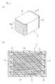
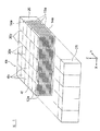
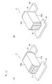
図1(A)に示すように、本実施形態に係る積層セラミックコンデンサ2は、素子本体4と、第1外部電極6と第2外部電極8とを有する。素子本体4は、図1(B)に示すように、第1内部電極層12および第2内部電極層13を有し、第1内側誘電体層10および第2内側誘電体層11の間に、これらの内部電極層12,13が交互に積層してある。
As shown in FIG. 1A, the multilayer
素子本体4は、その積層方向の両端面に、外側誘電体層14を有する。交互に積層される一方の第1内部電極層12は、素子本体4の第1端部の外側に形成してある第1外部電極6の内側に対して電気的に接続してある。また、交互に積層される他方の第2内部電極層13は、素子本体4の第2端部の外側に形成してある第2外部電極8の内側に対して電気的に接続してある。
The
第1および第2内側誘電体層10,11および外側誘電体層14の材質は、特に限定されず、たとえばチタン酸カルシウム、チタン酸ストロンチウムおよび/またはチタン酸バリウムなどの誘電体材料で構成される。各内側誘電体層10,11の厚みは、特に限定されないが、数μm〜数十μmのものが一般的である。また、外側誘電体層14からなる外層部の厚みは、特に限定されないが、好ましくは10〜200μmの範囲である。
The materials of the first and second inner
第1および第2外部電極6,8の材質も特に限定されないが、通常、Ni,Pd,Ag,Au,Cu,Pt,Rh,Ru,Ir,Sn,Ti等の少なくとも1種、又はそれらの合金を用いることができる。通常は、Cu,Cu合金、Ni又はNi合金等や、Ag,Ag−Pd合金、In−Ga合金等が使用される。外部電極6,8の厚みも特に限定されないが、例えば、5〜30μm程度とすることができる。
The material of the first and second
積層セラミックコンデンサ2の形状やサイズは、目的や用途に応じて適宜決定すればよい。積層セラミックコンデンサ2は、通常、縦0.2〜5.7mm×横0.1〜5.0mm×厚み0.1〜3.2mm程度である。
The shape and size of the multilayer
次に、本発明の一実施形態としての積層セラミックコンデンサ2の製造方法について説明する。
Next, the manufacturing method of the multilayer
まず、図2〜図5に示すシート積層体4aを形成する。このシート積層体4aを形成するために、図3に示すように、第1内部電極パターン12aが形成される第1グリーンシート10aと、第2内部電極パターン13aが形成される第2グリーンシート11aを交互に積層し、シート積層体4aを形成する。
First, the
グリーンシート10a,11aを形成するための誘電体用ペーストは、通常、セラミック粉末と有機ビヒクルとを混練して得られた有機溶剤系ペースト、または水系ペーストで構成される。本実施形態では、これらのペーストは、有機溶剤系ペーストであることが好ましい。
The dielectric paste for forming the
なお、有機ビヒクルとは、バインダを有機溶剤中に溶解したものである。有機ビヒクルに用いるバインダは特に限定されず、エチルセルロース、ポリビニルブチラール等の通常の各種バインダから適宜選択すればよい。 The organic vehicle is obtained by dissolving a binder in an organic solvent. The binder used for the organic vehicle is not particularly limited, and may be appropriately selected from usual various binders such as ethyl cellulose and polyvinyl butyral.
内部電極パターン12a,13aは、グリーンシート10a,11aの表面に形成される。内部電極パターン12a,13aを形成するための内部電極用ペーストは、各種導電性金属や合金からなる導電材、あるいは焼成後に導電材となる各種酸化物、有機金属化合物、レジネート等と、上記した有機ビヒクルとを混練して調製する。なお、内部電極用ペーストには、必要に応じて、共材としてセラミック粉末が含まれていても良い。共材は、焼成過程において導電性粉末の焼結を抑制する作用を奏する。
The
グリーンシート10a,11aは、上記の誘電体用ペーストを用いたドクターブレード法などで形成される。また、グリーンシート10a,11aの各表面に内部電極パターン12a,13aを形成するには、上記の内部電極用ペーストを用いてスクリーン印刷などを行えばよい。
The
シート積層体4aにおける第1グリーンシート10aは、最終的には図1に示す第1内側誘電体層10となる部分であり、第2グリーンシート11aは、最終的には図1に示す第2内側誘電体層11となる部分である。また、第1内部電極パターン12aは、最終的には図1に示す第1内部電極層12となる部分であり、第2内部電極パターン13aは、最終的には図1に示す第2内部電極層13となる部分である。
The first
図3では、図示の容易化のために、シート積層体4aにおける内部電極パターン12aおよび13aの積層数を少なく図示してあるが、数層から数百層と自由に設定することができる。
In FIG. 3, for ease of illustration, the number of laminated
なお、図2および図3に示すように、シート積層体4aにおける積層方向Zの両端部には、外側誘電体層14となるべきグリーンシート14aが積層してある。シート積層体4aにおける積層方向Zの厚みは、焼成後において、図1に示す素子本体4の厚みに対応する。
As shown in FIGS. 2 and 3,
図2および図3に示すように、シート積層体4aにおいて、第1内部電極パターン12aと第2内部電極パターン13aとは、パターン12a,13aの電極長手方向X(以下、X軸とも言う)に沿って、半パターンずらしてある長方形の繰り返しパターンである。
As shown in FIGS. 2 and 3, in the
また、パターン12a,13aの電極長手方向Xと積層方向Z(以下、Z軸とも言う)との双方に垂直であるシート積層体4aの電極切断方向Y(以下、Y軸または積層体長手方向Yとも言う)に沿って見れば、第1内部電極パターン12aと第2内部電極パターン13aとは、同じピッチ長さの分離した長方形パターン(図2参照)である。
Further, the electrode cutting direction Y (hereinafter referred to as Y axis or laminate longitudinal direction Y) of the
なお、図2に示すように、これらの第1内部電極パターン12aおよび第2内部電極パターン13aは、シート積層体4aのY軸に沿って両端位置には形成されない領域が存在し、その領域が端部切り捨て部分26となる。
As shown in FIG. 2, the first
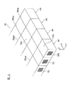
図2および図3では、シート積層体4aと素子本体要素4bとの関係を分かりやすくするために、最終的な切断予定線30x,30yを図示してある。なお、素子本体要素4bは、図1に示す素子本体4となる部分である。図2および図3に示す切断予定線30x,30yの通りに最終的に切断するために、この実施形態では、図4に示すように、シート積層体4aの最外表面4f(積層方向Zに直交する表面)に、電極ペーストによる印刷法で、切断位置マーク30aを形成してある。
2 and 3,
それらの切断位置マーク30aを複数のカメラ32で読み取ることにより、シート積層体4aの位置合わせを行い、図5に示すように、マーキング用押切刃34で、シート積層体4aの表面に、マーキング用切り溝30xa,30yaを形成する。
The cutting position marks 30a are read by a plurality of
この実施形態では、図5に示すマーキング用切り溝30xa,30yaは、図2および図3に示す切断予定線30x,30yに対応し、マトリックス状に形成される。マーキング用切り溝30xa,30yaの溝深さは、特に限定されず、シート積層体4aを焼成後にも、それらのマーキング用切り溝30xa,30yaをカメラにより認識できる程度であればよい。
In this embodiment, the marking grooves 30xa and 30ya shown in FIG. 5 correspond to the
次に、この実施形態では、マーキング用切り溝30xa,30yaが形成されたシート積層体4aに対して、脱バインダ処理および焼成処理を施し、図6に示す焼結後のシート積層体4cを得る。脱バインダ処理および焼成処理の諸条件は特に限定されないが、焼成温度としては、たとえば1000〜1400°Cである。
Next, in this embodiment, the
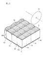
その後に、図6に示すように、焼結後のシート積層体4cの表面に形成してある切断位置マーク30aを、複数のカメラ32で読み取り、シート積層体4cの位置決めを行う。その後に、図7に示すように、スライサーの回転切断刃36を用いて、焼結後のシート積層体4cを、マーキング用切り溝30yaに沿って切断分離し、図8および図9に示す複数の棒状積層体4dを得る。
After that, as shown in FIG. 6, the
図8は、焼結後のシート積層体4cを、マーキング用切り溝30yaに沿って切断した直後の状態を示す斜視図である。棒状積層体4dは、電極切断方向Yと一致する積層体長手方向Yに細長い棒状の形状を有している。切断された直後のマーキング用切り溝30yaは、図2および図3に示す切断予定線30yに対応し、棒状積層体4dの第1切断面30bには、内部電極層12または13が露出する。すなわち、棒状積層体4dの一方の第1切断面30bには、第2内部電極層13が露出しており、他方の第1切断面30bには、第1内部電極層12が露出している。
FIG. 8 is a perspective view showing a state immediately after the
また、棒状積層体4dは、内部電極層12,13に略平行であって、積層方向Zに略垂直な側面30cを有する。側面30cは、切断前のシート積層体4cにおいて、積層方向Zに垂直な最外表面4fであった面である。
The rod-shaped
なお、本実施形態では、シート積層体4aを焼結した後に、焼結後のシート積層体4cを、マーキング用切り溝30yaに沿って切断したが、焼結および切断は、これと逆の順番であってもよい。すなわち、シート積層体4aを、マーキング用切り溝30yaに沿って切断した後に焼結することによって、棒状積層体4dを作製してもよい。
In this embodiment, after the
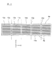
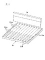
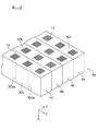
次に、本実施形態に係る製造方法では、複数の棒状積層体4dを、再配列して、図10に示す積層体集合体4eを作製する。積層体集合体4eを作製するために、まず、図8に示す棒状積層体4dを、図9に示すように回転させて、棒状積層体4dの側面30cおよび第1切断面30bの向きを変更する。
Next, in the manufacturing method according to the present embodiment, a plurality of rod-
図8に示すように、棒状積層体4dの姿勢を変更する前において、棒状積層体4dの側面30cは、棒状積層体4dの設置面に対して略平行であり、第1切断面30bは、設置面に対して略垂直である。図9に示すように、棒状積層体4dの姿勢を変更させた後において、棒状積層体4dの側面30cは、棒状積層体4dの設置面に対して略垂直であり、第1切断面30bは、設置面に対して略平行である。
As shown in FIG. 8, before changing the posture of the bar-shaped
さらに、姿勢を変更させた棒状積層体4dを、互いに側面30cが密着するように配列して、積層体集合体4eを作製する。各棒状積層体4dの寸法は略同一であるため、棒状積層体4dの第1切断面30bは、図10に示すように、略同一の平面に沿って配列される。したがって、積層体集合体4eの一方の面は、第2内部電極層13が露出する第1切断面30bによって構成され、積層体集合体4eの他方の面は、第1内部電極層12が露出する第1切断面30bによって構成される。
Furthermore, the
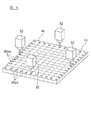
積層体集合体4eには、図11に示すように、溝部52が形成される。溝部52は、積層体集合体4eを構成する棒状積層体4dの第1切断面30bに形成される。溝部52は、例えばV字状のカッター、ブラスト、レーザー等によって、積層体集合体4eの一部を切除することによって形成する。
As shown in FIG. 11, a
溝部52は、棒状積層体4dの電極長手方向X(X軸方向)および積層体長手方向切Y(Y軸方向)に直交する積層方向Z(Z軸方向)に沿って形成される。また、溝部52は、図2に示す切断予定線30xに沿って形成される。したがって、溝部52は、図11に示すように、各棒状積層体4dのマーキング用切り溝30xaを通過する。
The
本実施形態に係る製造方法において、溝部52は、棒状積層体4dの第1切断面30bのうち、第1内部電極層12が露出している第1切断面30bと、第2内部電極層13が露出している第1切断面30bの両方に形成される。第1切断面30bに形成される溝部52の形状としては、特に限定されないが、溝部52の側部52bが、切断予定線30xの近傍から切断予定線30xへ向かって傾斜する略V字状の形状を有することが好ましい。また、溝部52は、最終切断工程で使用する回転切断刃36の刃幅や、溝部52の表面に形成される外部電極6,8の厚さ等を考慮して、平坦な底部52aを有していても良い。
In the manufacturing method according to the present embodiment, the
溝部52の形状は、溝部52を形成する前に、溝部52を形成するためのブレードの形状等を変更したり、ブラストまたはレーザー等の出力を調整することによって、変更・制御してもよい。溝部52の形状を制御することによって、最終的に得られるセラミックコンデンサ2における外部電極6,8の形状が変わるため、セラミックコンデンサ2の実装強度を最適化することができる。例えば、溝部52の形状を制御し、外部電極6,8の面積を拡大することによって、実装時におけるセラミックコンデンサ2の固着強度(セラミックコンデンサ2が実装基板から剥がれないでくっついている耐性)を高めることができる。また、溝部52の形状を制御し、外部電極6,8の面積拡大を抑制することによって、実装時におけるセラミックコンデンサ2の撓み強度(セラミックコンデンサ2が実装された基板が外力で撓む場合に、セラミックコンデンサ2と実装基板の電気的接続が維持される耐性。固着強度とトレードオフとなる場合がある。)を高めることができる。
The shape of the
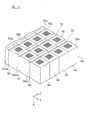
本実施形態に係る製造方法では、図12に示すように、棒状積層体4dの第1切断面30bに溝部52を形成した後、積層体集合体4eを構成する棒状積層体4dの第1切断面30bに、外部電極6,8を薄膜形成する。外部電極6,8を薄膜形成する方法としては、特に限定されないが、例えばスパッタ法や、蒸着法等を用いることができる。なお、積層方向Zに沿って溝部52を形成した後に、外部電極6,8の形成を行うことによって、例えば焼成時において内部電極12,13の引き込みが発生した場合にでも、内部電極12,13と、外部電極6,8を導通させることができる。第1切断面30bを切除して溝部52を形成することによって、焼成時に引き込まれた内部電極12,13を露出させることができるからである。
In the manufacturing method according to the present embodiment, as shown in FIG. 12, after the
外部電極6,8を形成した後に、最終切断工程を行う。最終切断工程では、図12に示すように、外部電極6,8が形成された棒状積層体4dを、スライサーの回転切断刃36によって、図2に示す切断予定線30xに沿って切断し、図13に示す個片状のセラミックコンデンサ2を得る。
After forming the
本実施形態に係る製造方法では、棒状積層体4dによって積層体集合体4eを構成した状態で、最終切断工程を行う。溝部52は、切断予定線30x(図2参照)に沿って形成されているので、最終切断工程では、図12に示すように、棒状積層体4dを、溝部52に沿って切断する。
In the manufacturing method according to the present embodiment, the final cutting step is performed in a state where the
本実施形態に係る最終切断工程では、溝部52に沿って棒状積層体4dを切断するため、個片状に切断する際にセラミックコンデンサ2の角部が欠けたり、角部付近に割れが発生したりすることを効果的に防止することができる。また、本実施形態に係る製造方法によって得られるセラミックコンデンサ2は、図13に示すように、セラミックコンデンサ2の角部が面取りされた形状を有しているため、輸送時等における割れ・欠け等の発生を抑制できる。
In the final cutting step according to the present embodiment, the rod-shaped
なお、本実施形態に係る製造方法では、外部電極6,8を形成した後に、最終切断工程を行ったが、外部電極6,8の形成は、最終切断工程の後に行っても良い。すなわち、図11に示す積層体集合体4eを、溝部52に沿って切断した後、個片に分離する前に、外部電極6,8を薄膜形成しても良い。
In the manufacturing method according to this embodiment, the final cutting process is performed after the
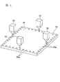
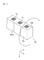
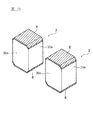
図14(A)および図14(B)は、セラミックコンデンサ2をランド54に対して配置する配置例を示した図である。セラミックコンデンサ2は、図14(A)に示すように、棒状積層体4dの側面30cであった面がランド54の実装面と略垂直となり、最終切断工程によって発生した面である第2切断面30eが実施面と略平行となるように配置することができる。また、セラミックコンデンサ2は、図14(B)に示すように、棒状積層体4dの側面30cであった面がランド54の実装面と略平行となり、第2切断面30eが実装面と略垂直になるように配置することもできる。
FIGS. 14A and 14B are diagrams showing an arrangement example in which the
本実施形態に係る積層セラミックコンデンサ2の製造方法では、複数の棒状積層体4dを再配列した積層体集合体4eを形成することによって、複数の棒状積層体4dに対して同時に外部電極6,8を薄膜形成することができる。複数の棒状積層体4dに対して一括で外部電極6,8の形成ができるため、本発明に係る製造方法は生産効率が良い。また、棒状積層体4dの側面30cを密着させることによって、外部電極6,8を構成する材料が、棒状積層体4dの側面30cに回り込むことを防止できる。そのため、回り込み防止のためにマスキング等の対策を行う工程を省略することができ、効率的な生産が可能である。
In the manufacturing method of the multilayer
本実施形態に係る製造方法によって得られるセラミックコンデンサ2は、直方体形状の対向面にのみ外部電極が形成されている従来技術に係るセラミックコンデンサに比べて、外部電極6,8の面積が広い。したがって、図12に示すセラミックコンデンサ2は、従来技術に係るセラミックコンデンサに比べて実装強度が高い。
The
また、本発明に係る積層電子部品の製造方法では、最終切断工程において、積層体集合体4eを構成する複数の棒状積層体4dを、溝部52に沿って切断する。これによって、切断時または切断後におけるセラミックコンデンサ2の角部欠けおよび割れ等を防止することができる。また、溝部52に沿って切断することにより、切断時の位置精度を向上させることができる。
In the method for manufacturing a laminated electronic component according to the present invention, the plurality of rod-
その他の実施形態
第1実施形態に係る製造方法では、図11に示すように、棒状積層体4dの切断面に溝部52を形成したが、溝部52と同様の溝部を、焼成後のシート積層体4cに形成してもよい。この場合、図7に示す焼成後のシート積層体4cにおける最外表面4fに、切断予定線30yに沿って、溝部を形成することができる。
Other Embodiments In the manufacturing method according to the first embodiment, as shown in FIG. 11, the
焼成後のシート積層体4cを、最外表面4fに形成された溝部に沿って切断し、棒状積層体4dを得ることによって、切断時の割れ、欠けを防止することができる。または、その後、第1実施形態と同様にして、セラミックコンデンサを作製することができる。このように作製されたセラミックコンデンサは、第1実施形態に係るセラミックコンデンサ2と同様に、外部電極の面積が広く、従来技術に係るセラミックコンデンサに比べて実装強度が高い。
By cutting the fired
また、セラミックコンデンサ2の製造方法は、第1実施形態に係る製造方法に含まれる工程に加えて、棒状積層体4dの側面30cまたは焼成後のシート積層体4cの最外表面4fを平滑化する工程を有していても良い。図10に示す積層体集合体を形成する前に、棒状積層体4dの側面30cまたは焼成後のシート積層体4cの最外表面4fを平滑化することによって、隣接する棒状積層体4dの側面30c同士の密着性を高めることができる。隣接する棒状積層体4dの側面30c同士の密着性を高めることによって、外部電極6,8を形成する工程において、側面30cに外部電極6,8の材料が付着することを防止することができる。
In addition to the steps included in the manufacturing method according to the first embodiment, the method for manufacturing the
棒状積層体4dの側面30cまたは焼成後のシート積層体4cの最外表面4fを平滑化する工程は、棒状積層体4dの側面30cまたは焼成後のシート積層体4cの最外表面4fを、機械的または化学的に研磨等することによって実施される。
The step of smoothing the
また、第1実施形態に係る製造方法では、図7に示す溝部52を形成する工程において、隣接する2つの溝部52は、棒状積層体4dの積層体長手方向Yに1つの素子本体要素4bを挟むように形成される。しかし、他の実施形態に係る製造方法では、溝部52を形成する工程において、隣接する2つの溝部52は、棒状積層体4dの積層体長手方向Yに2つの素子本体要素4bを挟むように形成されてもよい。このようにして得られたセラミックコンデンサは、図11に示すセラミックコンデンサ2とは異なり、片側の2つの辺のみが面取りされた形状を有しているが、セラミックコンデンサ2と同様の効果を有する。
In the manufacturing method according to the first embodiment, in the step of forming the
2… 積層セラミックコンデンサ
4… 素子本体
4a… シート積層体
4b… 素子本体要素
4d… 棒状積層体
6… 第1外部電極
8… 第2外部電極
10… 第1内側誘電体層
10a… 第1グリーンシート
11… 第2内側誘電体層
11a… 第2グリーンシート
12… 第1内部電極層
12a… 第1内部電極パターン
13… 第2内部電極層
13a… 第2内部電極パターン
30b… 第1切断面
30c… 側面
30x,30y… 切断予定線
30xa,30ya… マーキング用切り溝
52… 溝部
2 ... multilayer
Claims (6)
前記シート積層体を焼成および切断することによって、前記内部電極層が露出する切断面と、前記シート積層体の積層方向に略垂直な側面とを有しており、長手方向に細長い複数の棒状積層体を形成する工程と、
前記複数の棒状積層体を再配列し、前記複数の棒状積層体の前記側面が互いに密着しており、前記複数の棒状積層体の前記切断面が略同一の平面に沿って配置された積層体集合体を形成する工程と、
前記積層体集合体を構成する前記棒状積層体の一部を切除し、前記棒状積層体の前記切断面に溝部を形成する工程と、
前記溝部が形成された前記積層体集合体における前記複数の棒状積層体の前記切断面に外部電極を薄膜形成する工程と、
前記棒状積層体を個片状に切断する工程と、を有する
積層セラミック電子部品の製造方法。 Preparing a sheet laminate in which an internal electrode pattern that becomes an internal electrode layer after firing and a green sheet that becomes a ceramic layer after firing are laminated;
By firing and cutting the sheet laminate, a plurality of rod-like laminates having a cut surface from which the internal electrode layer is exposed and a side surface substantially perpendicular to the stacking direction of the sheet laminate are elongated in the longitudinal direction. Forming a body;
The laminated body in which the plurality of rod-like laminated bodies are rearranged, the side surfaces of the plurality of rod-like laminated bodies are in close contact with each other, and the cut surfaces of the plurality of rod-like laminated bodies are arranged along substantially the same plane. Forming an aggregate;
Cutting a part of the rod-like laminate constituting the laminate aggregate and forming a groove in the cut surface of the rod-like laminate; and
Forming an external electrode in a thin film on the cut surface of the plurality of rod-like laminates in the laminate assembly in which the groove is formed ;
Cutting the rod-shaped laminate into individual pieces, and a method for producing a multilayer ceramic electronic component.
請求項1から請求項3までのいずれか1項に記載された積層セラミック電子部品の製造方法。 The method for manufacturing a multilayer ceramic electronic component according to claim 1, further comprising a step of controlling the shape of the groove.
請求項1から請求項5までのいずれか1項に記載された積層セラミック電子部品の製造方法。 The method for producing a multilayer ceramic electronic component according to any one of claims 1 to 5, further comprising a step of smoothing a surface of the fired sheet laminate.
Priority Applications (1)
| Application Number | Priority Date | Filing Date | Title |
|---|---|---|---|
| JP2009086588A JP5218219B2 (en) | 2009-03-31 | 2009-03-31 | Manufacturing method of multilayer ceramic electronic component |
Applications Claiming Priority (1)
| Application Number | Priority Date | Filing Date | Title |
|---|---|---|---|
| JP2009086588A JP5218219B2 (en) | 2009-03-31 | 2009-03-31 | Manufacturing method of multilayer ceramic electronic component |
Publications (2)
| Publication Number | Publication Date |
|---|---|
| JP2010238991A JP2010238991A (en) | 2010-10-21 |
| JP5218219B2 true JP5218219B2 (en) | 2013-06-26 |
Family
ID=43093050
Family Applications (1)
| Application Number | Title | Priority Date | Filing Date |
|---|---|---|---|
| JP2009086588A Active JP5218219B2 (en) | 2009-03-31 | 2009-03-31 | Manufacturing method of multilayer ceramic electronic component |
Country Status (1)
| Country | Link |
|---|---|
| JP (1) | JP5218219B2 (en) |
Families Citing this family (5)
| Publication number | Priority date | Publication date | Assignee | Title |
|---|---|---|---|---|
| JP5780169B2 (en) * | 2011-03-14 | 2015-09-16 | 株式会社村田製作所 | Manufacturing method of multilayer ceramic electronic component |
| JP5590054B2 (en) * | 2012-02-07 | 2014-09-17 | 株式会社村田製作所 | Manufacturing method of multilayer ceramic electronic component |
| JP6179480B2 (en) * | 2013-09-20 | 2017-08-16 | 株式会社村田製作所 | Capacitor element manufacturing method and manufacturing apparatus |
| JP6648689B2 (en) | 2016-12-28 | 2020-02-14 | 株式会社村田製作所 | Manufacturing method of multilayer electronic component and multilayer electronic component |
| JP6648690B2 (en) | 2016-12-28 | 2020-02-14 | 株式会社村田製作所 | Manufacturing method of multilayer electronic component and multilayer electronic component |
Family Cites Families (5)
| Publication number | Priority date | Publication date | Assignee | Title |
|---|---|---|---|---|
| JPS57155717A (en) * | 1981-03-20 | 1982-09-25 | Matsushita Electric Industrial Co Ltd | Method of producing chip part |
| JPH0696990A (en) * | 1992-09-16 | 1994-04-08 | Matsushita Electric Ind Co Ltd | Production of multilayer ceramic chip component |
| JPH06132182A (en) * | 1992-10-19 | 1994-05-13 | Tdk Corp | Manufacture of small electronic parts |
| JPH07115008A (en) * | 1993-10-15 | 1995-05-02 | Matsushita Electric Ind Co Ltd | Manufacturing method of chip resistor |
| JP3384309B2 (en) * | 1997-12-16 | 2003-03-10 | 松下電器産業株式会社 | Manufacturing method of multiple electronic components |
-
2009
- 2009-03-31 JP JP2009086588A patent/JP5218219B2/en active Active
Also Published As
| Publication number | Publication date |
|---|---|
| JP2010238991A (en) | 2010-10-21 |
Similar Documents
| Publication | Publication Date | Title |
|---|---|---|
| CN103247442B (en) | The manufacture method of monolithic ceramic electronic component | |
| CN113140405B (en) | Multilayer ceramic capacitor | |
| JP5218219B2 (en) | Manufacturing method of multilayer ceramic electronic component | |
| JP4983873B2 (en) | Laminated electronic components | |
| JP4358220B2 (en) | Multilayer piezoelectric element | |
| JP2017212272A (en) | Multilayer ceramic capacitor | |
| JP5141046B2 (en) | Multilayer piezoelectric element | |
| TWI482185B (en) | Laminated ceramic capacitors | |
| KR102166591B1 (en) | Method for manufacturing multilayer ceramic electronic component | |
| JP7283221B2 (en) | Electronic component manufacturing method | |
| JP2015111652A (en) | Electronic component | |
| JP2015109409A (en) | Electronic component | |
| JP4692539B2 (en) | Manufacturing method of multilayer electronic component | |
| JP2015111654A (en) | Method of manufacturing laminated electric component and laminated electronic component | |
| JP4561826B2 (en) | Manufacturing method of multilayer electronic component | |
| JPH09260187A (en) | Manufacture of ceramic electronic part | |
| JP2008166385A (en) | Manufacturing method of laminated inductor | |
| JP4502130B2 (en) | Manufacturing method of laminated electronic component | |
| JP4525733B2 (en) | Manufacturing method of multilayer electronic component | |
| JP5444593B2 (en) | Multilayer piezoelectric element | |
| JP2009164189A (en) | Manufacturing method of multilayer ceramic electronic component | |
| JP2010238989A (en) | Method for manufacturing laminated ceramic electronic component | |
| WO2014125930A1 (en) | Ceramic electronic component and method for producing same | |
| JP2011003847A (en) | Method of manufacturing ceramic electronic component | |
| JP4539489B2 (en) | Manufacturing method of multilayer capacitor |
Legal Events
| Date | Code | Title | Description |
|---|---|---|---|
| A621 | Written request for application examination |
Free format text: JAPANESE INTERMEDIATE CODE: A621 Effective date: 20111101 |
|
| A977 | Report on retrieval |
Free format text: JAPANESE INTERMEDIATE CODE: A971007 Effective date: 20121108 |
|
| A131 | Notification of reasons for refusal |
Free format text: JAPANESE INTERMEDIATE CODE: A131 Effective date: 20121113 |
|
| A521 | Request for written amendment filed |
Free format text: JAPANESE INTERMEDIATE CODE: A523 Effective date: 20130115 |
|
| RD02 | Notification of acceptance of power of attorney |
Free format text: JAPANESE INTERMEDIATE CODE: A7422 Effective date: 20130115 |
|
| TRDD | Decision of grant or rejection written | ||
| A01 | Written decision to grant a patent or to grant a registration (utility model) |
Free format text: JAPANESE INTERMEDIATE CODE: A01 Effective date: 20130205 |
|
| A61 | First payment of annual fees (during grant procedure) |
Free format text: JAPANESE INTERMEDIATE CODE: A61 Effective date: 20130218 |
|
| FPAY | Renewal fee payment (event date is renewal date of database) |
Free format text: PAYMENT UNTIL: 20160315 Year of fee payment: 3 |
|
| R150 | Certificate of patent or registration of utility model |
Ref document number: 5218219 Country of ref document: JP Free format text: JAPANESE INTERMEDIATE CODE: R150 Free format text: JAPANESE INTERMEDIATE CODE: R150 |
|
| R250 | Receipt of annual fees |
Free format text: JAPANESE INTERMEDIATE CODE: R250 |
|
| R250 | Receipt of annual fees |
Free format text: JAPANESE INTERMEDIATE CODE: R250 |