JP5216446B2 - Plasma CVD apparatus and display device manufacturing method - Google Patents
Plasma CVD apparatus and display device manufacturing method Download PDFInfo
- Publication number
- JP5216446B2 JP5216446B2 JP2008172141A JP2008172141A JP5216446B2 JP 5216446 B2 JP5216446 B2 JP 5216446B2 JP 2008172141 A JP2008172141 A JP 2008172141A JP 2008172141 A JP2008172141 A JP 2008172141A JP 5216446 B2 JP5216446 B2 JP 5216446B2
- Authority
- JP
- Japan
- Prior art keywords
- plasma
- layer
- semiconductor layer
- gas
- processing chamber
- Prior art date
- Legal status (The legal status is an assumption and is not a legal conclusion. Google has not performed a legal analysis and makes no representation as to the accuracy of the status listed.)
- Expired - Fee Related
Links
- 238000004519 manufacturing process Methods 0.000 title claims description 30
- 238000005268 plasma chemical vapour deposition Methods 0.000 title claims description 30
- 239000004065 semiconductor Substances 0.000 claims description 152
- 238000012545 processing Methods 0.000 claims description 97
- 239000000758 substrate Substances 0.000 claims description 49
- 238000000034 method Methods 0.000 claims description 27
- 239000010410 layer Substances 0.000 description 299
- 239000007789 gas Substances 0.000 description 119
- 239000010408 film Substances 0.000 description 36
- 239000003990 capacitor Substances 0.000 description 32
- 239000012535 impurity Substances 0.000 description 27
- 230000015572 biosynthetic process Effects 0.000 description 24
- 239000004973 liquid crystal related substance Substances 0.000 description 22
- 239000001307 helium Substances 0.000 description 19
- 229910052734 helium Inorganic materials 0.000 description 19
- SWQJXJOGLNCZEY-UHFFFAOYSA-N helium atom Chemical compound [He] SWQJXJOGLNCZEY-UHFFFAOYSA-N 0.000 description 19
- 239000001257 hydrogen Substances 0.000 description 17
- 229910052739 hydrogen Inorganic materials 0.000 description 17
- BLRPTPMANUNPDV-UHFFFAOYSA-N Silane Chemical compound [SiH4] BLRPTPMANUNPDV-UHFFFAOYSA-N 0.000 description 15
- 230000001681 protective effect Effects 0.000 description 15
- UFHFLCQGNIYNRP-UHFFFAOYSA-N Hydrogen Chemical compound [H][H] UFHFLCQGNIYNRP-UHFFFAOYSA-N 0.000 description 14
- 229910052710 silicon Inorganic materials 0.000 description 13
- XKRFYHLGVUSROY-UHFFFAOYSA-N Argon Chemical compound [Ar] XKRFYHLGVUSROY-UHFFFAOYSA-N 0.000 description 12
- 229910052581 Si3N4 Inorganic materials 0.000 description 12
- 229910052782 aluminium Inorganic materials 0.000 description 12
- XAGFODPZIPBFFR-UHFFFAOYSA-N aluminium Chemical compound [Al] XAGFODPZIPBFFR-UHFFFAOYSA-N 0.000 description 12
- 239000000463 material Substances 0.000 description 12
- 239000010703 silicon Substances 0.000 description 12
- HQVNEWCFYHHQES-UHFFFAOYSA-N silicon nitride Chemical compound N12[Si]34N5[Si]62N3[Si]51N64 HQVNEWCFYHHQES-UHFFFAOYSA-N 0.000 description 12
- IJGRMHOSHXDMSA-UHFFFAOYSA-N Atomic nitrogen Chemical compound N#N IJGRMHOSHXDMSA-UHFFFAOYSA-N 0.000 description 11
- 238000000151 deposition Methods 0.000 description 9
- XUIMIQQOPSSXEZ-UHFFFAOYSA-N Silicon Chemical compound [Si] XUIMIQQOPSSXEZ-UHFFFAOYSA-N 0.000 description 8
- 230000008021 deposition Effects 0.000 description 8
- 229910052990 silicon hydride Inorganic materials 0.000 description 8
- 239000011521 glass Substances 0.000 description 7
- 239000011229 interlayer Substances 0.000 description 7
- 229910000077 silane Inorganic materials 0.000 description 7
- VYPSYNLAJGMNEJ-UHFFFAOYSA-N silicon dioxide Inorganic materials O=[Si]=O VYPSYNLAJGMNEJ-UHFFFAOYSA-N 0.000 description 7
- 229910021417 amorphous silicon Inorganic materials 0.000 description 6
- 229910052786 argon Inorganic materials 0.000 description 6
- QVGXLLKOCUKJST-UHFFFAOYSA-N atomic oxygen Chemical compound [O] QVGXLLKOCUKJST-UHFFFAOYSA-N 0.000 description 6
- 238000005530 etching Methods 0.000 description 6
- 229910052751 metal Inorganic materials 0.000 description 6
- 239000002184 metal Substances 0.000 description 6
- 229910021424 microcrystalline silicon Inorganic materials 0.000 description 6
- 239000001301 oxygen Substances 0.000 description 6
- 229910052760 oxygen Inorganic materials 0.000 description 6
- -1 silicon halide Chemical class 0.000 description 6
- 230000004888 barrier function Effects 0.000 description 5
- 238000010790 dilution Methods 0.000 description 5
- 239000012895 dilution Substances 0.000 description 5
- 229910021420 polycrystalline silicon Inorganic materials 0.000 description 5
- 229910052814 silicon oxide Inorganic materials 0.000 description 5
- RYGMFSIKBFXOCR-UHFFFAOYSA-N Copper Chemical compound [Cu] RYGMFSIKBFXOCR-UHFFFAOYSA-N 0.000 description 4
- PXGOKWXKJXAPGV-UHFFFAOYSA-N Fluorine Chemical compound FF PXGOKWXKJXAPGV-UHFFFAOYSA-N 0.000 description 4
- RTAQQCXQSZGOHL-UHFFFAOYSA-N Titanium Chemical compound [Ti] RTAQQCXQSZGOHL-UHFFFAOYSA-N 0.000 description 4
- 229910052802 copper Inorganic materials 0.000 description 4
- 239000010949 copper Substances 0.000 description 4
- 239000011737 fluorine Substances 0.000 description 4
- 229910052731 fluorine Inorganic materials 0.000 description 4
- 230000001771 impaired effect Effects 0.000 description 4
- 238000005499 laser crystallization Methods 0.000 description 4
- 229910052757 nitrogen Inorganic materials 0.000 description 4
- 238000000926 separation method Methods 0.000 description 4
- 239000010409 thin film Substances 0.000 description 4
- 229910052719 titanium Inorganic materials 0.000 description 4
- 239000010936 titanium Substances 0.000 description 4
- VYZAMTAEIAYCRO-UHFFFAOYSA-N Chromium Chemical compound [Cr] VYZAMTAEIAYCRO-UHFFFAOYSA-N 0.000 description 3
- ZOKXTWBITQBERF-UHFFFAOYSA-N Molybdenum Chemical compound [Mo] ZOKXTWBITQBERF-UHFFFAOYSA-N 0.000 description 3
- 229910052804 chromium Inorganic materials 0.000 description 3
- 239000011651 chromium Substances 0.000 description 3
- PMHQVHHXPFUNSP-UHFFFAOYSA-M copper(1+);methylsulfanylmethane;bromide Chemical compound Br[Cu].CSC PMHQVHHXPFUNSP-UHFFFAOYSA-M 0.000 description 3
- 238000005520 cutting process Methods 0.000 description 3
- 229910001873 dinitrogen Inorganic materials 0.000 description 3
- 229910052736 halogen Inorganic materials 0.000 description 3
- 150000002367 halogens Chemical class 0.000 description 3
- 238000010438 heat treatment Methods 0.000 description 3
- 150000002431 hydrogen Chemical class 0.000 description 3
- 239000011261 inert gas Substances 0.000 description 3
- 239000011810 insulating material Substances 0.000 description 3
- 229910052743 krypton Inorganic materials 0.000 description 3
- DNNSSWSSYDEUBZ-UHFFFAOYSA-N krypton atom Chemical compound [Kr] DNNSSWSSYDEUBZ-UHFFFAOYSA-N 0.000 description 3
- 229910052750 molybdenum Inorganic materials 0.000 description 3
- 239000011733 molybdenum Substances 0.000 description 3
- 229910052754 neon Inorganic materials 0.000 description 3
- GKAOGPIIYCISHV-UHFFFAOYSA-N neon atom Chemical compound [Ne] GKAOGPIIYCISHV-UHFFFAOYSA-N 0.000 description 3
- 230000003647 oxidation Effects 0.000 description 3
- 238000007254 oxidation reaction Methods 0.000 description 3
- 229920005591 polysilicon Polymers 0.000 description 3
- 238000000746 purification Methods 0.000 description 3
- 238000007348 radical reaction Methods 0.000 description 3
- 239000003870 refractory metal Substances 0.000 description 3
- 239000000523 sample Substances 0.000 description 3
- 125000006850 spacer group Chemical group 0.000 description 3
- CURLTUGMZLYLDI-UHFFFAOYSA-N Carbon dioxide Chemical compound O=C=O CURLTUGMZLYLDI-UHFFFAOYSA-N 0.000 description 2
- 238000001069 Raman spectroscopy Methods 0.000 description 2
- XLOMVQKBTHCTTD-UHFFFAOYSA-N Zinc monoxide Chemical compound [Zn]=O XLOMVQKBTHCTTD-UHFFFAOYSA-N 0.000 description 2
- 125000004429 atom Chemical group 0.000 description 2
- 239000000460 chlorine Substances 0.000 description 2
- 238000004140 cleaning Methods 0.000 description 2
- 238000004891 communication Methods 0.000 description 2
- 238000011109 contamination Methods 0.000 description 2
- 239000013078 crystal Substances 0.000 description 2
- 238000007872 degassing Methods 0.000 description 2
- 230000005669 field effect Effects 0.000 description 2
- 238000011049 filling Methods 0.000 description 2
- 238000011010 flushing procedure Methods 0.000 description 2
- 125000002887 hydroxy group Chemical group [H]O* 0.000 description 2
- 239000012528 membrane Substances 0.000 description 2
- 239000007769 metal material Substances 0.000 description 2
- 239000013081 microcrystal Substances 0.000 description 2
- 239000010453 quartz Substances 0.000 description 2
- 239000012495 reaction gas Substances 0.000 description 2
- 238000003860 storage Methods 0.000 description 2
- 238000006557 surface reaction Methods 0.000 description 2
- 229910052715 tantalum Inorganic materials 0.000 description 2
- GUVRBAGPIYLISA-UHFFFAOYSA-N tantalum atom Chemical compound [Ta] GUVRBAGPIYLISA-UHFFFAOYSA-N 0.000 description 2
- ZOXJGFHDIHLPTG-UHFFFAOYSA-N Boron Chemical compound [B] ZOXJGFHDIHLPTG-UHFFFAOYSA-N 0.000 description 1
- OKTJSMMVPCPJKN-UHFFFAOYSA-N Carbon Chemical compound [C] OKTJSMMVPCPJKN-UHFFFAOYSA-N 0.000 description 1
- ZAMOUSCENKQFHK-UHFFFAOYSA-N Chlorine atom Chemical compound [Cl] ZAMOUSCENKQFHK-UHFFFAOYSA-N 0.000 description 1
- 229910052779 Neodymium Inorganic materials 0.000 description 1
- OAICVXFJPJFONN-UHFFFAOYSA-N Phosphorus Chemical compound [P] OAICVXFJPJFONN-UHFFFAOYSA-N 0.000 description 1
- 239000004642 Polyimide Substances 0.000 description 1
- 229910003902 SiCl 4 Inorganic materials 0.000 description 1
- NRTOMJZYCJJWKI-UHFFFAOYSA-N Titanium nitride Chemical compound [Ti]#N NRTOMJZYCJJWKI-UHFFFAOYSA-N 0.000 description 1
- 230000002159 abnormal effect Effects 0.000 description 1
- 238000010521 absorption reaction Methods 0.000 description 1
- NIXOWILDQLNWCW-UHFFFAOYSA-N acrylic acid group Chemical group C(C=C)(=O)O NIXOWILDQLNWCW-UHFFFAOYSA-N 0.000 description 1
- 230000003321 amplification Effects 0.000 description 1
- 229910052785 arsenic Inorganic materials 0.000 description 1
- RQNWIZPPADIBDY-UHFFFAOYSA-N arsenic atom Chemical compound [As] RQNWIZPPADIBDY-UHFFFAOYSA-N 0.000 description 1
- 229910052796 boron Inorganic materials 0.000 description 1
- 229910052799 carbon Inorganic materials 0.000 description 1
- 229910002092 carbon dioxide Inorganic materials 0.000 description 1
- 239000001569 carbon dioxide Substances 0.000 description 1
- 229910010293 ceramic material Inorganic materials 0.000 description 1
- 239000007795 chemical reaction product Substances 0.000 description 1
- 238000005229 chemical vapour deposition Methods 0.000 description 1
- 229910052801 chlorine Inorganic materials 0.000 description 1
- SLLGVCUQYRMELA-UHFFFAOYSA-N chlorosilicon Chemical compound Cl[Si] SLLGVCUQYRMELA-UHFFFAOYSA-N 0.000 description 1
- 230000003749 cleanliness Effects 0.000 description 1
- 239000011248 coating agent Substances 0.000 description 1
- 238000000576 coating method Methods 0.000 description 1
- 239000004020 conductor Substances 0.000 description 1
- 238000002425 crystallisation Methods 0.000 description 1
- 230000008025 crystallization Effects 0.000 description 1
- 230000003247 decreasing effect Effects 0.000 description 1
- 230000007547 defect Effects 0.000 description 1
- 230000003111 delayed effect Effects 0.000 description 1
- 238000013461 design Methods 0.000 description 1
- 238000003745 diagnosis Methods 0.000 description 1
- 238000009792 diffusion process Methods 0.000 description 1
- 238000007865 diluting Methods 0.000 description 1
- 239000003085 diluting agent Substances 0.000 description 1
- PZPGRFITIJYNEJ-UHFFFAOYSA-N disilane Chemical compound [SiH3][SiH3] PZPGRFITIJYNEJ-UHFFFAOYSA-N 0.000 description 1
- 238000001312 dry etching Methods 0.000 description 1
- 239000007772 electrode material Substances 0.000 description 1
- 238000005265 energy consumption Methods 0.000 description 1
- 238000001704 evaporation Methods 0.000 description 1
- 239000010419 fine particle Substances 0.000 description 1
- QUZPNFFHZPRKJD-UHFFFAOYSA-N germane Chemical compound [GeH4] QUZPNFFHZPRKJD-UHFFFAOYSA-N 0.000 description 1
- 229910052732 germanium Inorganic materials 0.000 description 1
- GNPVGFCGXDBREM-UHFFFAOYSA-N germanium atom Chemical compound [Ge] GNPVGFCGXDBREM-UHFFFAOYSA-N 0.000 description 1
- GGJOARIBACGTDV-UHFFFAOYSA-N germanium difluoride Chemical compound F[Ge]F GGJOARIBACGTDV-UHFFFAOYSA-N 0.000 description 1
- 229910052986 germanium hydride Inorganic materials 0.000 description 1
- AMGQUBHHOARCQH-UHFFFAOYSA-N indium;oxotin Chemical compound [In].[Sn]=O AMGQUBHHOARCQH-UHFFFAOYSA-N 0.000 description 1
- 230000009191 jumping Effects 0.000 description 1
- 238000005259 measurement Methods 0.000 description 1
- VNWKTOKETHGBQD-UHFFFAOYSA-N methane Chemical compound C VNWKTOKETHGBQD-UHFFFAOYSA-N 0.000 description 1
- 238000002156 mixing Methods 0.000 description 1
- 239000000203 mixture Substances 0.000 description 1
- 229910021421 monocrystalline silicon Inorganic materials 0.000 description 1
- QEFYFXOXNSNQGX-UHFFFAOYSA-N neodymium atom Chemical compound [Nd] QEFYFXOXNSNQGX-UHFFFAOYSA-N 0.000 description 1
- 229910052756 noble gas Inorganic materials 0.000 description 1
- 238000003199 nucleic acid amplification method Methods 0.000 description 1
- 239000002245 particle Substances 0.000 description 1
- 238000005192 partition Methods 0.000 description 1
- 230000000149 penetrating effect Effects 0.000 description 1
- 229910052698 phosphorus Inorganic materials 0.000 description 1
- 239000011574 phosphorus Substances 0.000 description 1
- 238000000206 photolithography Methods 0.000 description 1
- 229920001721 polyimide Polymers 0.000 description 1
- 230000001902 propagating effect Effects 0.000 description 1
- 239000011241 protective layer Substances 0.000 description 1
- 238000007670 refining Methods 0.000 description 1
- 229910052706 scandium Inorganic materials 0.000 description 1
- SIXSYDAISGFNSX-UHFFFAOYSA-N scandium atom Chemical compound [Sc] SIXSYDAISGFNSX-UHFFFAOYSA-N 0.000 description 1
- 238000007650 screen-printing Methods 0.000 description 1
- HBMJWWWQQXIZIP-UHFFFAOYSA-N silicon carbide Chemical compound [Si+]#[C-] HBMJWWWQQXIZIP-UHFFFAOYSA-N 0.000 description 1
- 229910010271 silicon carbide Inorganic materials 0.000 description 1
- 229910052709 silver Inorganic materials 0.000 description 1
- 239000004332 silver Substances 0.000 description 1
- 238000001179 sorption measurement Methods 0.000 description 1
- 238000004544 sputter deposition Methods 0.000 description 1
- 230000006641 stabilisation Effects 0.000 description 1
- 238000011105 stabilization Methods 0.000 description 1
- 229910001220 stainless steel Inorganic materials 0.000 description 1
- 239000010935 stainless steel Substances 0.000 description 1
- 230000002459 sustained effect Effects 0.000 description 1
- XOLBLPGZBRYERU-UHFFFAOYSA-N tin dioxide Chemical compound O=[Sn]=O XOLBLPGZBRYERU-UHFFFAOYSA-N 0.000 description 1
- 229910001887 tin oxide Inorganic materials 0.000 description 1
- 238000012546 transfer Methods 0.000 description 1
- 238000011144 upstream manufacturing Methods 0.000 description 1
- 238000007740 vapor deposition Methods 0.000 description 1
- 238000001039 wet etching Methods 0.000 description 1
- 239000011787 zinc oxide Substances 0.000 description 1
Images


Classifications
-
- G—PHYSICS
- G02—OPTICS
- G02F—OPTICAL DEVICES OR ARRANGEMENTS FOR THE CONTROL OF LIGHT BY MODIFICATION OF THE OPTICAL PROPERTIES OF THE MEDIA OF THE ELEMENTS INVOLVED THEREIN; NON-LINEAR OPTICS; FREQUENCY-CHANGING OF LIGHT; OPTICAL LOGIC ELEMENTS; OPTICAL ANALOGUE/DIGITAL CONVERTERS
- G02F1/00—Devices or arrangements for the control of the intensity, colour, phase, polarisation or direction of light arriving from an independent light source, e.g. switching, gating or modulating; Non-linear optics
- G02F1/01—Devices or arrangements for the control of the intensity, colour, phase, polarisation or direction of light arriving from an independent light source, e.g. switching, gating or modulating; Non-linear optics for the control of the intensity, phase, polarisation or colour
- G02F1/13—Devices or arrangements for the control of the intensity, colour, phase, polarisation or direction of light arriving from an independent light source, e.g. switching, gating or modulating; Non-linear optics for the control of the intensity, phase, polarisation or colour based on liquid crystals, e.g. single liquid crystal display cells
- G02F1/1303—Apparatus specially adapted to the manufacture of LCDs
-
- C—CHEMISTRY; METALLURGY
- C23—COATING METALLIC MATERIAL; COATING MATERIAL WITH METALLIC MATERIAL; CHEMICAL SURFACE TREATMENT; DIFFUSION TREATMENT OF METALLIC MATERIAL; COATING BY VACUUM EVAPORATION, BY SPUTTERING, BY ION IMPLANTATION OR BY CHEMICAL VAPOUR DEPOSITION, IN GENERAL; INHIBITING CORROSION OF METALLIC MATERIAL OR INCRUSTATION IN GENERAL
- C23C—COATING METALLIC MATERIAL; COATING MATERIAL WITH METALLIC MATERIAL; SURFACE TREATMENT OF METALLIC MATERIAL BY DIFFUSION INTO THE SURFACE, BY CHEMICAL CONVERSION OR SUBSTITUTION; COATING BY VACUUM EVAPORATION, BY SPUTTERING, BY ION IMPLANTATION OR BY CHEMICAL VAPOUR DEPOSITION, IN GENERAL
- C23C16/00—Chemical coating by decomposition of gaseous compounds, without leaving reaction products of surface material in the coating, i.e. chemical vapour deposition [CVD] processes
- C23C16/44—Chemical coating by decomposition of gaseous compounds, without leaving reaction products of surface material in the coating, i.e. chemical vapour deposition [CVD] processes characterised by the method of coating
- C23C16/50—Chemical coating by decomposition of gaseous compounds, without leaving reaction products of surface material in the coating, i.e. chemical vapour deposition [CVD] processes characterised by the method of coating using electric discharges
- C23C16/511—Chemical coating by decomposition of gaseous compounds, without leaving reaction products of surface material in the coating, i.e. chemical vapour deposition [CVD] processes characterised by the method of coating using electric discharges using microwave discharges
-
- G—PHYSICS
- G02—OPTICS
- G02F—OPTICAL DEVICES OR ARRANGEMENTS FOR THE CONTROL OF LIGHT BY MODIFICATION OF THE OPTICAL PROPERTIES OF THE MEDIA OF THE ELEMENTS INVOLVED THEREIN; NON-LINEAR OPTICS; FREQUENCY-CHANGING OF LIGHT; OPTICAL LOGIC ELEMENTS; OPTICAL ANALOGUE/DIGITAL CONVERTERS
- G02F1/00—Devices or arrangements for the control of the intensity, colour, phase, polarisation or direction of light arriving from an independent light source, e.g. switching, gating or modulating; Non-linear optics
- G02F1/01—Devices or arrangements for the control of the intensity, colour, phase, polarisation or direction of light arriving from an independent light source, e.g. switching, gating or modulating; Non-linear optics for the control of the intensity, phase, polarisation or colour
- G02F1/13—Devices or arrangements for the control of the intensity, colour, phase, polarisation or direction of light arriving from an independent light source, e.g. switching, gating or modulating; Non-linear optics for the control of the intensity, phase, polarisation or colour based on liquid crystals, e.g. single liquid crystal display cells
- G02F1/133—Constructional arrangements; Operation of liquid crystal cells; Circuit arrangements
- G02F1/136—Liquid crystal cells structurally associated with a semi-conducting layer or substrate, e.g. cells forming part of an integrated circuit
- G02F1/1362—Active matrix addressed cells
-
- H—ELECTRICITY
- H01—ELECTRIC ELEMENTS
- H01J—ELECTRIC DISCHARGE TUBES OR DISCHARGE LAMPS
- H01J37/00—Discharge tubes with provision for introducing objects or material to be exposed to the discharge, e.g. for the purpose of examination or processing thereof
- H01J37/32—Gas-filled discharge tubes
- H01J37/32009—Arrangements for generation of plasma specially adapted for examination or treatment of objects, e.g. plasma sources
- H01J37/32192—Microwave generated discharge
-
- H—ELECTRICITY
- H01—ELECTRIC ELEMENTS
- H01L—SEMICONDUCTOR DEVICES NOT COVERED BY CLASS H10
- H01L21/00—Processes or apparatus adapted for the manufacture or treatment of semiconductor or solid state devices or of parts thereof
- H01L21/02—Manufacture or treatment of semiconductor devices or of parts thereof
- H01L21/02104—Forming layers
- H01L21/02107—Forming insulating materials on a substrate
- H01L21/02225—Forming insulating materials on a substrate characterised by the process for the formation of the insulating layer
- H01L21/0226—Forming insulating materials on a substrate characterised by the process for the formation of the insulating layer formation by a deposition process
- H01L21/02263—Forming insulating materials on a substrate characterised by the process for the formation of the insulating layer formation by a deposition process deposition from the gas or vapour phase
- H01L21/02271—Forming insulating materials on a substrate characterised by the process for the formation of the insulating layer formation by a deposition process deposition from the gas or vapour phase deposition by decomposition or reaction of gaseous or vapour phase compounds, i.e. chemical vapour deposition
- H01L21/02274—Forming insulating materials on a substrate characterised by the process for the formation of the insulating layer formation by a deposition process deposition from the gas or vapour phase deposition by decomposition or reaction of gaseous or vapour phase compounds, i.e. chemical vapour deposition in the presence of a plasma [PECVD]
-
- H—ELECTRICITY
- H01—ELECTRIC ELEMENTS
- H01L—SEMICONDUCTOR DEVICES NOT COVERED BY CLASS H10
- H01L21/00—Processes or apparatus adapted for the manufacture or treatment of semiconductor or solid state devices or of parts thereof
- H01L21/02—Manufacture or treatment of semiconductor devices or of parts thereof
- H01L21/02104—Forming layers
- H01L21/02365—Forming inorganic semiconducting materials on a substrate
- H01L21/02656—Special treatments
- H01L21/02664—Aftertreatments
- H01L21/02667—Crystallisation or recrystallisation of non-monocrystalline semiconductor materials, e.g. regrowth
Landscapes
- Physics & Mathematics (AREA)
- Chemical & Material Sciences (AREA)
- Engineering & Computer Science (AREA)
- Plasma & Fusion (AREA)
- General Physics & Mathematics (AREA)
- Nonlinear Science (AREA)
- Crystallography & Structural Chemistry (AREA)
- Manufacturing & Machinery (AREA)
- Microelectronics & Electronic Packaging (AREA)
- Chemical Kinetics & Catalysis (AREA)
- Optics & Photonics (AREA)
- Power Engineering (AREA)
- Metallurgy (AREA)
- General Chemical & Material Sciences (AREA)
- Analytical Chemistry (AREA)
- Materials Engineering (AREA)
- Mechanical Engineering (AREA)
- Organic Chemistry (AREA)
- Condensed Matter Physics & Semiconductors (AREA)
- Computer Hardware Design (AREA)
- Mathematical Physics (AREA)
- Thin Film Transistor (AREA)
- Liquid Crystal (AREA)
- Plasma Technology (AREA)
- Electroluminescent Light Sources (AREA)
Description
本発明は、微結晶半導体の作製方法、微結晶半導体薄膜トランジスタにより構成される表示装置の作製方法に関する。 The present invention relates to a method for manufacturing a microcrystalline semiconductor and a method for manufacturing a display device including a microcrystalline semiconductor thin film transistor.
既に液晶ディスプレイの用途において、薄膜トランジスタ(以下、「TFT」とも記す。)は広く用いられている。TFTは電界効果トランジスタの一種であり、チャネルを形成する半導体が薄膜で形成される。チャネルを形成する半導体層がアモルファスシリコンで形成されるものと多結晶シリコンで形成されるものがあり、前者は液晶テレビジョンなどの大画面パネルにおいて、後者は携帯電話機のモニタ画面など小型高精細の用途において使われている。 Thin film transistors (hereinafter also referred to as “TFTs”) have already been widely used in liquid crystal display applications. A TFT is a kind of field effect transistor, and a semiconductor forming a channel is formed of a thin film. The semiconductor layer forming the channel is made of amorphous silicon and polycrystalline silicon. The former is a large screen panel such as a liquid crystal television, and the latter is a small high definition such as a monitor screen of a mobile phone. Used in applications.
ところで、微結晶シリコンはアモルファスシリコンと並び、古くから知られた材料であり、電界効果型トランジスタに関するものについては1980年代に報告されている(例えば、特許文献1参照)。しかしながら、今日に至るまで微結晶シリコンを用いたTFTは、アモルファスシリコントランジスタと多結晶シリコントランジスタの間に埋もれて実用化が遅れている。微結晶シリコンは、学会レベルで報告されている(例えば、非特許文献1参照)。
微結晶シリコン膜は、シランなどの水素化珪素気体を水素で多量希釈して、プラズマを利用した化学的気相成長法(プラズマCVD法)により形成される。この場合、成膜条件を最適化しても微結晶シリコン膜を成膜する速度は0.1nm/秒以下であった。概略100nm以上の膜厚を必要とするTFTにおいて、このような成膜速度の遅いプロセスを採用することは実用的でなかった。即ち、アモルファスシリコンTFTと比べて生産性が悪いという問題があった。 The microcrystalline silicon film is formed by a chemical vapor deposition method (plasma CVD method) using plasma by diluting a large amount of silicon hydride gas such as silane with hydrogen. In this case, the speed at which the microcrystalline silicon film was formed was 0.1 nm / second or less even when the film formation conditions were optimized. In a TFT requiring a film thickness of approximately 100 nm or more, it has not been practical to employ such a process with a slow film formation rate. That is, there is a problem that productivity is poor as compared with the amorphous silicon TFT.
本発明はこのような問題を解決するものであり、気相成長法で形成される微結晶半導体層の成膜速度を向上させ、微結晶半導体のTFTにより構成される表示装置の生産性を向上させることを目的とする。また本発明は、微結晶半導体のTFTを生産する製造装置を提供することを目的とする。 The present invention solves these problems, and improves the deposition rate of a microcrystalline semiconductor layer formed by a vapor deposition method and improves the productivity of a display device including a microcrystalline semiconductor TFT. The purpose is to let you. Another object of the present invention is to provide a manufacturing apparatus for producing a microcrystalline semiconductor TFT.
並置された複数の導波管と、壁面とで囲まれた処理室にヘリウムを含む反応性気体を供給する手段等を備えた製造装置において、ヘリウムを含む反応性気体を供給し、処理室内の圧力を大気圧若しくは準大気圧に保持しつつ、並置された導波管で挟まれた空間にマイクロ波を供給してプラズマを生成し、処理室内に載置された基板上に微結晶半導体でなる微結晶半導体層を堆積する。反応性気体はヘリウムに加えて、半導体材料ガスや希釈ガスが含まれる。 In a manufacturing apparatus including a plurality of waveguides juxtaposed and a means for supplying a reactive gas containing helium to a processing chamber surrounded by a wall surface, the reactive gas containing helium is supplied, While maintaining the pressure at atmospheric pressure or quasi-atmospheric pressure, microwaves are supplied to the space between the juxtaposed waveguides to generate plasma, and a microcrystalline semiconductor is formed on the substrate placed in the processing chamber. A microcrystalline semiconductor layer is deposited. The reactive gas includes semiconductor material gas and dilution gas in addition to helium.
並置された複数の導波管の対向する面にスリットが設けられ、該スリットを介して処理室内にマイクロ波が供給されることによりプラズマが生成される。このように生成されたプラズマは安定したものである。プラズマを生成するとき処理室の圧力は大気圧若しくは準大気圧であり、代表的には、1×10²Pa以上1×10⁵Pa以下(1Torr以上760Torr以下)の圧力が適用される。安定化が図られたプラズマを用いることで、1×10²Pa以上1×10⁵Pa以下(1Torr以上760Torr以下)の圧力で水素と水素化珪素気体若しくはハロゲン化珪素気体を反応せしめ、微結晶半導体層を形成する。並置された導波管で挟まれた空間に安定して高密度なプラズマを生成することができるため、本発明の微結晶半導体層を概略1×10²Pa以上1×10⁵Pa以下の圧力であっても安定して形成することができる。 Slits are provided on the opposing surfaces of the plurality of waveguides juxtaposed, and plasma is generated by supplying microwaves into the processing chamber through the slits. The plasma generated in this way is stable. When generating plasma, the pressure in the processing chamber is atmospheric pressure or sub-atmospheric pressure, and typically, a pressure of 1 × 10 2 Pa to 1 × 10 5 Pa (1 Torr to 760 Torr) is applied. By using stabilized plasma, hydrogen and a silicon hydride gas or a silicon halide gas are reacted at a pressure of 1 × 10 2 Pa to 1 × 10 5 Pa (1 Torr to 760 Torr or less) to form microcrystals. A semiconductor layer is formed. Since a high-density plasma can be stably generated in a space sandwiched between juxtaposed waveguides, the microcrystalline semiconductor layer of the present invention has a pressure of approximately 1 × 10 2 Pa to 1 × 10 5 Pa. Even so, it can be formed stably.
微結晶半導体層は微小な結晶構造を半導体膜中に含み、自由エネルギー的に安定な第3の状態を有する半導体であって、短距離秩序を持ち格子歪みを有する結晶質なものである。当該結晶は概略2nm〜100nmのサイズを有している。電子顕微鏡では当該結晶は柱状若しくは錐形状の形状で観測することができる。微結晶半導体層は格子歪みを有し、例えば微結晶シリコン膜をラマン分光法で観測すると、単結晶シリコンの520.7cm−1と非晶質シリコンの480cm−1の間であって、代表的には514cm−1から519cm−1の間にラマンピークがみられ、格子歪みを有することがわかる。また、未結合手(ダングリングボンド)を補償するものとして水素またはハロゲンを含ませるとよい。水素又はハロゲンは、少なくとも1原子%またはそれ以上含ませる。さらに、ヘリウム、アルゴン、クリプトン、ネオンなどの希ガスを含ませて格子歪みをさらに助長させた微結晶半導体もある。 The microcrystalline semiconductor layer is a semiconductor that includes a microcrystalline structure in a semiconductor film and has a third state that is stable in terms of free energy and has a short-range order and a lattice distortion. The crystal has a size of approximately 2 nm to 100 nm. In an electron microscope, the crystal can be observed in a columnar or conical shape. Microcrystalline semiconductor layer has a lattice strain, for example, a microcrystalline silicon film observed by Raman spectroscopy, be between 520.7Cm -1 and the amorphous silicon 480 cm -1 of single crystal silicon, a representative , A Raman peak is observed between 514 cm −1 and 519 cm −1 , and it can be seen that it has lattice distortion. In addition, hydrogen or halogen is preferably included as compensation for dangling bonds. Hydrogen or halogen is contained in at least 1 atomic% or more. Further, there is a microcrystalline semiconductor in which a rare gas such as helium, argon, krypton, or neon is included to further promote lattice distortion.
微結晶半導体の成膜時の圧力を大気圧若しくは準大気圧として、安定なマイクロ波プラズマを生成することにより、成膜速度を低下させずに微結晶半導体を作製することができる。そのような微結晶半導体層でTFTを作製することが可能である。微結晶半導体層でチャネルが形成されるTFTはアモルファスシリコンTFTに比べ電気的特性が優れている。この発明によれば、微結晶半導体層でチャネルが形成されるTFTで表示装置を製造する際にも、生産性を損なうことがない。本発明の微結晶半導体層は、従来と比較して、50倍程度の堆積速度で形成することができる。 By generating a stable microwave plasma by setting the pressure at the time of film formation of the microcrystalline semiconductor to atmospheric pressure or quasi-atmospheric pressure, the microcrystalline semiconductor can be manufactured without reducing the film formation rate. A TFT can be manufactured using such a microcrystalline semiconductor layer. A TFT in which a channel is formed with a microcrystalline semiconductor layer has superior electrical characteristics as compared with an amorphous silicon TFT. According to the present invention, productivity is not impaired even when a display device is manufactured using a TFT in which a channel is formed of a microcrystalline semiconductor layer. The microcrystalline semiconductor layer of the present invention can be formed at a deposition rate about 50 times that of the conventional one.
本発明の実施の形態について、図面を用いて以下に説明する。但し、本発明は以下の説明に限定されず、本発明の趣旨及びその範囲から逸脱することなくその形態及び詳細をさまざまに変更し得ることは当業者であれば容易に理解される。従って、本発明は以下に示す実施の形態の記載内容に限定して解釈されるものではない。以下に説明する本発明の構成において、同じものを指す符号は異なる図面間で共通して用いる。 Embodiments of the present invention will be described below with reference to the drawings. However, the present invention is not limited to the following description, and it will be easily understood by those skilled in the art that modes and details can be variously changed without departing from the spirit and scope of the present invention. Therefore, the present invention should not be construed as being limited to the description of the embodiments below. In the structure of the present invention described below, the same reference numerals are used in common in different drawings.
(マルチ・チャンバ・マイクロ波プラズマCVD装置の一構成例)
微結晶半導体層はプラズマCVD法により作製する。本形態では微結晶半導体層の成膜条件として、大気圧若しくは準大気圧の圧力が適用される。この圧力として代表的な範囲は1×10²Pa以上1×10⁵Pa以下(1Torr以上760Torr以下)である。この圧力で生成されるプラズマは、電子密度が1×1011cm−3以上1×1013cm−3以下であり、電子温度が0.2eV以上2.0eV以下(より好ましくは0.5eV以上1.5eV以下)程度であるものを用いることが好ましい。電子密度が高く、電子温度が低いプラズマを利用するとプラズマダメージが少ないため、欠陥が少ない良質な微結晶半導体層を形成することができる。
(One configuration example of a multi-chamber microwave plasma CVD apparatus)
The microcrystalline semiconductor layer is formed by a plasma CVD method. In this embodiment mode, atmospheric pressure or quasi-atmospheric pressure is applied as the deposition condition of the microcrystalline semiconductor layer. A typical range for this pressure is 1 × 10 2 Pa or more and 1 × 10 5 Pa or less (1 Torr or more and 760 Torr or less). The plasma generated at this pressure has an electron density of 1 × 10 11 cm −3 or more and 1 × 10 13 cm −3 or less, and an electron temperature of 0.2 eV or more and 2.0 eV or less (more preferably 0.5 eV or more). It is preferable to use one having a level of about 1.5 eV or less. When plasma with high electron density and low electron temperature is used, plasma damage is small, so that a high-quality microcrystalline semiconductor layer with few defects can be formed.
このようなプラズマを生成するために、好適にはマイクロ波電力がプラズマCVD装置の処理室に供給される。液晶用のガラス基板のような大面積のマザーガラス基板に対しても、高密度のプラズマを作用させるために、処理室へは導波管によってマイクロ波電力が供給されるとよい。処理室の構成として、導波管は複数並置され、導波管にはスリットが設けられる。スリットは、互いに隣接した導波管が対向する面にマイクロ波が漏洩するよう設けられる。並置された導波管で挟まれた空間にマイクロ波を供給してプラズマを生成し、水素と、希釈された水素化珪素気体若しくはハロゲン化珪素気体とに作用させることで微結晶半導体層を成膜することができる。以下に微結晶半導体層を成膜するのに適した装置の一例を示す。 In order to generate such plasma, microwave power is preferably supplied to the processing chamber of the plasma CVD apparatus. Microwave power is preferably supplied to the processing chamber by a waveguide in order to cause a high-density plasma to act on a mother glass substrate having a large area such as a glass substrate for liquid crystal. As a configuration of the processing chamber, a plurality of waveguides are juxtaposed, and a slit is provided in the waveguide. The slit is provided so that the microwave leaks to the surface where the adjacent waveguides face each other. A microcrystalline semiconductor layer is formed by supplying a microwave to a space sandwiched between juxtaposed waveguides to generate plasma and reacting with hydrogen and diluted silicon hydride gas or silicon halide gas. Can be membrane. An example of an apparatus suitable for forming a microcrystalline semiconductor layer is described below.
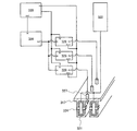
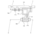
図1は複数の処理室を備えたマルチ・チャンバ・マイクロ波プラズマCVD装置の一例を示す。この装置は共通室306と、ロード/アンロード室301、第1処理室302、第2処理室303、第3処理室304を備えた構成となっている。ロード/アンロード室301のカセット308に装填される素子基板は、共通室306の搬送機構309によって各処理室に搬出入され、プラズマCVD装置は枚葉式の構成となる。共通室306と各室の間にはゲートバルブ307が備えられ、各処理室で行われる処理が、相互に干渉しないように構成されている。各処理室は形成する薄膜の種類によって区分されている。例えば、第1処理室302ではゲート絶縁膜などの絶縁膜を成膜し、第2処理室303ではチャネルを形成する微結晶半導体層を成膜し、第3処理室304ではソース及びドレインを形成する一導電型の不純物半導体層を成膜する。勿論、処理室の数はこれに限定されるわけではなく、必要に応じて任意に増減することができる。また、上述のように一の処理室で一の膜を成膜するようにしても良いし、一の処理室で複数の膜を成膜するように構成しても良い。
FIG. 1 shows an example of a multi-chamber microwave plasma CVD apparatus provided with a plurality of processing chambers. This apparatus includes a
各処理室内は不活性ガス又は窒素ガスで置換され、概略1×10²Pa以上1×10⁵Pa以下の圧力で反応ガスを流すことができるように、ガス供給手段312、排気手段310が接続されている。本装置による成膜は大気圧若しくは準大気圧で行われるので、排気手段310は吸引排気能力が高いものが好ましい。排気手段310と各処理室との間には開閉制御バルブ311が設けられており、これによって排気速度を制御することもできる。
The gas supply means 312 and the exhaust means 310 are connected so that each processing chamber is replaced with an inert gas or nitrogen gas, and the reaction gas can flow at a pressure of approximately 1 × 10 2 Pa to 1 × 10 5 Pa. Has been. Since film formation by this apparatus is performed at atmospheric pressure or quasi-atmospheric pressure, it is preferable that the exhaust means 310 has a high suction exhaust capability. An open /
ガス供給手段312はシリンダ313、バルブ314、流量制御機器315などで構成されており、シリンダ313には半導体材料ガス若しくは希ガスなどプロセスに用いる処理用ガス等が充填されている。希ガスとしてヘリウムを用いた場合、プラズマを安定に発生させることもできる。ガス供給手段312gは第1処理室302に接続され、ゲート絶縁膜を成膜するための処理用ガスを供給する。ガス供給手段312iは第2処理室303に接続され、チャネルを形成するi型半導体層用のガスを供給する。ガス供給手段312nは第3処理室304に接続され、ソース及びドレインを形成するn型半導体層用のガスを供給する。ガス供給手段312hは水素を供給し、ガス供給手段312fは処理室内のクリーニングに用いるエッチングガスを供給する系統であり、これらは各処理室共通のラインとして構成されている。
The gas supply means 312 includes a
各処理室にはプラズマ発生手段305が設けられている。プラズマ発生手段305は処理室内でプラズマを発生させる発振器が含まれる。例えば、マイクロ波電源、マイクロ波増幅器とマイクロ波を処理室まで誘導する導波管などで構成される。プラズマ発生手段305は各処理室において一又は複数設けられている。プラズマ発生手段305は、被処理基板の面積に対して成膜される被膜の均一性を維持するために必要な数だけ設ければ良い。 Each processing chamber is provided with plasma generating means 305. The plasma generating means 305 includes an oscillator that generates plasma in the processing chamber. For example, it includes a microwave power source, a microwave amplifier, and a waveguide that guides the microwave to the processing chamber. One or a plurality of plasma generating means 305 are provided in each processing chamber. The number of plasma generation means 305 may be provided as many as necessary to maintain the uniformity of the film formed on the area of the substrate to be processed.
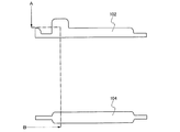
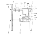
図2は処理室の一例を説明する断面図である。処理室は処理容器316と蓋体317とからなる。処理容器316は壁面を有しており、蓋体317は並置された複数の導波管321を有している。処理容器316と、蓋体317との密閉構造により圧力を概略1×10²Pa以上1×10⁵Pa以下に保持できる。処理容器316は、例えば、ステンレス鋼、アルミニウムなどの金属で形成されている。蓋体317と処理容器316で密閉空間が形成される処理室内は不活性ガス又は窒素ガスで置換可能となるようにガス供給手段312が設けられている。この処理室に接続される排気手段310によって処理室に供給したガスを排出することができる。処理室内は雰囲気を置換するために真空排気するようにしても良く、その場合、排気手段310を真空ポンプで構成しても良い。
FIG. 2 is a cross-sectional view illustrating an example of a processing chamber. The processing chamber includes a
処理容器316の内部には基板など被処理体を載置するサセプタ318が設けられている。サセプタ318は窒化アルミニウム、窒化シリコン、シリコンカーバイトなどのセラミックス材で構成されている。サセプタ318の内部には、ヒータ319が設けられている。ヒータ319はヒータ電源320に接続されている。ヒータ319はサセプタ318に埋め込まれており、ヒータ電源320から電力が供給されることにより発熱し、サセプタ318に載置された基板を所定の温度に保持する。
A
蓋体317は処理容器316の上部を密閉する。蓋体317が有する導波管321は、複数が並置され、櫛歯状に突出している。導波管321はマイクロ波電源322と連結されている。導波管321にはスリット323が設けられ、そこからマイクロ波が漏洩するようになっている。漏洩するとは、スリット323はマイクロ波を透過する誘電体板324で塞がれており、誘電体板324を介してマイクロ波が供給される状態を示す。誘電体板324は、導波管321の中に処理用ガスが流れ込まないようにスリット323を塞いでおり、石英などから形成される。誘電体板324は、プラズマを均一に発生させるため、導波管321の中央に配置されている。スリット323の位置は、導波管321の側面、つまり並置された導波管が互いに対向する側に設けられており、スリットも互いに対向している。
The
ガス供給手段312は、処理用ガス(反応性気体)が充填されたシリンダ313、バルブ314、流量制御機器315などで構成されている。流量制御機器315で流量が調整された処理用ガスは処理容器316内に供給される。シリンダ313は微結晶半導体の成膜に必要な処理用ガスが充填されている。成膜に必要な処理用ガスとしては、水素若しくはフッ素、又はヘリウム若しくはアルゴンなどの希ガスと、シラン若しくはジシランなどの半導体材料ガスとが含まれる。処理容器316にはガス供給ノズル325、ガス供給ノズル326があり、当該ノズルから処理用ガスが処理容器316内に流れ出す構成となっている。例えば、ガス供給ノズル325には水素若しくはフッ素、又はヘリウム若しくはアルゴンなどの希ガスを供給し、マイクロ波が供給される誘電体板324の近傍で高密度のラジカルを生成させる。高密度のラジカルによって、被処理基板上で微結晶半導体の成長表面における表面反応を促進させる。ガス供給ノズル326には被膜堆積用の半導体材料ガスを供給する。このように、ガスの供給経路を分離することで、誘電体板324への被膜の堆積を抑えることができる。成膜の段階では、ガス供給ノズル325から水素若しくはフッ素、又はヘリウム若しくはアルゴンなどの希ガスを供給し続けても良い。
The gas supply means 312 includes a
マイクロ波は誘電体板324を通して処理室内に供給される。導波管321を2mm以上10mm以下といった狭い間隔で並置してスリット323を対向する面に設けることにより、導波管321で挟まれた空間に高密度のプラズマを生成することができる。例えば、誘電体板324の表面を伝搬する表面波を利用して表面波プラズマを形成すると、高密度で均一なプラズマを形成することができる。この場合、導波管321で挟まれた狭い空間、つまり上記狭い間隔にプラズマを形成するので、概略1×10²Pa以上1×10⁵Pa以下の圧力であっても安定してプラズマを形成することができる。導波管の間隔は2mm以上10mm以下の範囲で、上記圧力が高いほど狭く、上記圧力が低いほど広くすることができる。
The microwave is supplied into the processing chamber through the
導波管321で挟まれた空間には、プラズマ発生器327が設けられている。プラズマ発生器327は、導波管321で挟まれた空間に、導波管321に沿って複数備えられている。プラズマ発生器327は、導波管321に接続されるものとは別のマイクロ波電源328に接続されている。マイクロ波電源328とプラズマ発生器327の間には電力増幅器329が設けられている。プラズマ発生器327は、導波管321へマイクロ波電力を投入して放電を開始するときに動作させ、プラズマ生成のきっかけをつくるために用いる。
A
プラズマ発生器327にはプラズマの状態を診断するプラズマモニタ機能が備えられており、その出力値が電力増幅器329に入力される。プラズマの状態を診断する方法としては、例えばラングミュアプローブなどが用いられ、電子密度や電子温度などを検出する。制御回路330には、処理室に設置された複数のプラズマ発生器327によりモニタされたプラズマの測定値が入力され、その値から処理室内のプラズマの密度が均一になるように、電力増幅器329のそれぞれに、増幅率を変える個別の制御信号を出力する。プラズマのジャンピング現象と呼ばれ、プラズマの高密度領域が放電空間内を遊動する現象を抑制するために有効である。
The
本形態のマイクロ波プラズマCVD装置は、導波管を複数に分割して並置することで、基板サイズの大型化に対しても均一なプラズマを生成することができる。基板サイズとしては、液晶ガラスで第1世代と呼ばれる300mm×400mmから、第3世代の550mm×650mm、第4世代の730mm×920mm、第5世代の1000mm×1200mm、第6世代の2450mm×1850mm、第7世代の1870mm×2200mm、第8世代の2000mm×2400mmなどで代表される各種の基板サイズに柔軟に対応することができる。 The microwave plasma CVD apparatus of this embodiment can generate a uniform plasma even when the substrate size is increased by dividing the waveguide into a plurality of pieces and juxtaposing the waveguides. As the substrate size, from 300 mm × 400 mm called the first generation in the liquid crystal glass, the third generation 550 mm × 650 mm, the fourth generation 730 mm × 920 mm, the fifth generation 1000 mm × 1200 mm, the sixth generation 2450 mm × 1850 mm, Various substrate sizes typified by the seventh generation 1870 mm × 2200 mm and the eighth generation 2000 mm × 2400 mm can be flexibly supported.
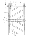
図3はこのような処理室の蓋体317と導波管321の構成を示す斜視図である。
導波管が2mm以上10mm以下といった狭い間隔で並置されることにより、これらに挟まれた細溝状の空間が形成されている。並置される導波管321の対向する面にスリット323を塞ぐ誘電体板324が設けられ、そこからマイクロ波が漏洩してプラズマを生成する。プラズマ発生器327は、並置される導波管321の細溝状の空間に沿って複数設けられている。
FIG. 3 is a perspective view showing the configuration of the
The waveguides are juxtaposed at a narrow interval of 2 mm or more and 10 mm or less, so that a narrow groove-like space is formed between them. A
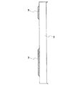
図4は蓋体317の構成を示す平面図である。蓋体317には導波管321が複数並置されている。導波管321にはスリット323が設けられ、そこからマイクロ波が漏洩するようになっている。スリット323の位置は並置される導波管321が対向する側に設けられている。スリット323は、導波管321の中に処理用ガスが流れ込まないように、マイクロ波を透過する誘電体板324で塞がれている。被処理基板の面積が大きい場合であっても、複数の導波管321を並置させ、その挟まれた空間にマイクロ波放電を生成することでプラズマ密度の均一化を図ることができる。さらに、当該空間には、並置された導波管321の間隔よりも広い間隔となるようにプラズマ発生器327を複数設け、電力増幅器329及び制御回路330によりプラズマ発生器327を制御してプラズマの安定化とプラズマ密度の均一化を図っている。このような構成により、本装置では730mm×920mmのガラス基板、若しくは一辺が1mを超えるサイズのガラス基板に対して処理を行うことができる。
FIG. 4 is a plan view showing the configuration of the
図5はプラズマ発生器327の一構成例を示す。ガスノズル331はガス供給手段312に接続されている。ガスノズル331の外側にはマイクロ波電力が供給される放電用電極332が設けられている。石英等でなるガスノズル331にはヘリウムなど放電開始電圧の低い非堆積性ガスが供給され、放電用電極332に電力が印加されることにより無電極放電が行われる。ガスノズル331の中で生成したプラズマは、ノズルの外側まで拡散する。このプラズマ発生器327を処理室に設けることで、ここで生成されたプラズマが放電開始のきっかけとなる。プローブ333はプラズマ診断用に用意されているものであり、例えばラングミュアプローブが適用される。このモニタ値は、電力増幅器329を介して制御回路330に入力される。
FIG. 5 shows a configuration example of the
図6は単室でゲート絶縁層から半導体層までを連続して成膜するマイクロ波プラズマCVD装置の一例を示す。第1処理室302とロード/アンロード室301等のその他の構成は図1と同様である。
FIG. 6 shows an example of a microwave plasma CVD apparatus for continuously forming a film from a gate insulating layer to a semiconductor layer in a single chamber. Other configurations such as the
第1処理室302は不活性ガス又は窒素ガスで置換され、概略1×10²Pa以上1×10⁵Pa以下の圧力で反応ガスを流すことができるように、ガス供給手段312と排気手段310が接続されている。ガス供給手段312は、シリンダ313、バルブ314、流量制御機器315などで構成されている。シリンダ313は、半導体材料ガス若しくは希ガスなどが充填されている。ガス供給手段312gは第1処理室302に接続され、ゲート絶縁層形成用のガスを供給する。ガス供給手段312iも第1処理室302に接続され、チャネル形成領域を構成するi型半導体層用のガスを供給する。ガス供給手段312nも第1処理室302に接続され、ソース及びドレインを構成するn型半導体層用のガスを供給する。ガス供給手段312hは水素を供給し、ガス供給手段312fは処理室内のクリーニングに用いるエッチングガスを供給する系統であり、これらは各処理室共通のラインとして構成されている。
The
処理室にはプラズマ発生手段305が設けられている。プラズマ発生手段305は処理室内でプラズマを発生させる発振器が含まれる。例えば、マイクロ波電源、マイクロ波増幅器とマイクロ波を処理室まで誘導する導波管などで構成される。プラズマ発生手段305は処理室において一又は複数設けられている。プラズマ発生手段305は、被処理基板の面積に対して成膜される被膜の均一性を維持するために必要な数だけ設ければ良い。 Plasma generating means 305 is provided in the processing chamber. The plasma generating means 305 includes an oscillator that generates plasma in the processing chamber. For example, it includes a microwave power source, a microwave amplifier, and a waveguide that guides the microwave to the processing chamber. One or a plurality of plasma generating means 305 are provided in the processing chamber. The number of plasma generation means 305 may be provided as many as necessary to maintain the uniformity of the film formed on the area of the substrate to be processed.
このような構成のプラズマCVD装置によっても、基板が載置された処理室内に反応性気体を供給し、基板と略平行に対向配置された導波管に設けられたスリットを介して処理室内にマイクロ波を供給する。そしてプラズマが生成され、基板上に微結晶半導体層を形成することができる。一つの処理室でゲート絶縁層と微結晶半導体層を積層形成する場合には、微結晶半導体層の形成前に放電を止めてSiH4ガスによる処理室内洗浄(フラッシング)を行っても良い。フラッシングにより、処理室内に残留する酸素、N2Oなどの残留不純物を効果的に除去することができる。 Even with the plasma CVD apparatus having such a configuration, a reactive gas is supplied into the processing chamber in which the substrate is placed, and the processing chamber is inserted into the processing chamber through a slit provided in the waveguide disposed so as to be substantially parallel to the substrate. Supply microwaves. Then, plasma is generated, and a microcrystalline semiconductor layer can be formed over the substrate. In the case where the gate insulating layer and the microcrystalline semiconductor layer are stacked in one treatment chamber, discharge may be stopped and flushing in the treatment chamber with SiH 4 gas may be performed before the formation of the microcrystalline semiconductor layer. By flushing, residual impurities such as oxygen and N 2 O remaining in the processing chamber can be effectively removed.
上記構成のプラズマCVD装置を用いて微結晶半導体の成膜をする場合には、処理室内でプラズマを発生させるときにヘリウムを用いることが好ましい。つまりプラズマを発生させる電力を供給する前にヘリウムを供給すると好ましい。ヘリウムは24.5eVとすべての気体中で最も高いイオン化エネルギーを持つが、そのイオン化エネルギーよりも少し低い、約20eVの準位に準安定状態があるので、放電持続中においては、イオン化するエネルギーには、差分となる約4eVしか必要とせず、安定した放電が持続できる。また放電開始電圧も全ての気体中最も低い値を示す。このような特性から、大気圧若しくは準大気圧における放電で、ヘリウムはプラズマを安定的に維持することができる。また、均一なプラズマを形成することができるので、微結晶半導体層を堆積する基板の面積が大きくなっても均一な膜を堆積することができる。 In the case where a microcrystalline semiconductor film is formed using the plasma CVD apparatus having the above structure, helium is preferably used when generating plasma in the treatment chamber. That is, it is preferable to supply helium before supplying power for generating plasma. Helium has the highest ionization energy of all gases at 24.5 eV, but there is a metastable state at a level of about 20 eV, which is slightly lower than the ionization energy. Requires only about 4 eV as a difference, and stable discharge can be sustained. Moreover, the discharge start voltage also shows the lowest value among all gases. From such characteristics, helium can stably maintain the plasma by discharge at atmospheric pressure or sub-atmospheric pressure. In addition, since uniform plasma can be formed, a uniform film can be deposited even when the area of the substrate on which the microcrystalline semiconductor layer is deposited is increased.
微結晶半導体層は、シラン(不純物を有する微結晶半導体とする場合には、シランに加えドーピングガスを用いる)と水素及び/又は希ガスを混合して高密度プラズマにより成膜する。シランは水素及び/又は希ガスで10倍から2000倍に希釈される。このような希釈に用いるガスを希釈ガスともよぶ。そのため多量の水素及び/又は希ガスが必要とされるため、微結晶半導体の成膜時に供給したガスは回収して再利用するとよい。図7はプラズマCVD装置に適用するガス精製循環装置334の一例を示す。
The microcrystalline semiconductor layer is formed by high-density plasma by mixing silane (in the case of a microcrystalline semiconductor having an impurity, a doping gas is used in addition to silane) and hydrogen and / or a rare gas. Silane is diluted 10 to 2000 times with hydrogen and / or a noble gas. A gas used for such dilution is also referred to as a dilution gas. Therefore, since a large amount of hydrogen and / or a rare gas is required, the gas supplied at the time of forming the microcrystalline semiconductor may be recovered and reused. FIG. 7 shows an example of a
ガス精製循環装置334としては、シランなどの半導体材料ガスを回収精製するもの、ヘリウムなどの希ガスを回収精製するものがある。ガス精製循環装置334は第1処理室302、第2処理室303、第3処理室304のそれぞれに設けることができる。第1処理室302にガス精製循環装置334が接続する場合で説明すると、第1処理室302の処理用ガスはサーキュレータ(循環機)等で構成される排気手段310から使用済みガスとして排出される。排気手段310から排出される使用済みガスはフィルタ335により微粒子が除去されて回収ガス容器336に蓄積される。回収ガス容器336に蓄積された後は、昇圧器337により昇圧され、分離器338によりヘリウムなどの希ガスのみを分離する。分離器338の構成としては、膜分離、吸着分離、吸収分離、深冷分離方式などが適用される。分離精製されたガスは充填容器339に蓄積される。充填容器339に蓄積されたガスは、圧力調整器340で所定の圧力に調整され、ガス供給手段312の流量制御機器315の上流側に供給される。このようにしてガスを再利用することで、微結晶半導体に必要なガスの消費量を削減することができる。すなわち、ヘリウムなどの希ガスを再利用することにより表示装置の製造に係る全エネルギー消費量を低減することができ、二酸化炭素の排出量を削減することができる。
Examples of the gas refining / circulating
本形態のマイクロ波プラズマCVD装置によれば、微結晶半導体層を大面積基板に均質に堆積することが可能である。以下、表示装置の製造工程の概略について説明する。 According to the microwave plasma CVD apparatus of this embodiment, a microcrystalline semiconductor layer can be uniformly deposited on a large-area substrate. Hereinafter, the outline of the manufacturing process of the display device will be described.
(実施の形態1)
微結晶半導体層でチャネルを形成するTFTにより構成される表示装置の一製造工程を図面を参照して説明する。図8、図9、図10、図11は画素の平面図を示し、当該図中に示すA−B切断線に対応する断面図を図12、図13、図14、図15、図16に示す。以下の説明ではこれら平面図と断面図を適宜参照しながら説明する。
(Embodiment 1)
One manufacturing process of a display device including a TFT which forms a channel with a microcrystalline semiconductor layer is described with reference to drawings. 8, 9, 10, and 11 are plan views of the pixel, and cross-sectional views corresponding to the A-B cutting line shown in the drawing are shown in FIGS. 12, 13, 14, 15, and 16. Show. The following description will be given with reference to these plan views and cross-sectional views as appropriate.
(1)ゲート電極及び容量電極の形成
TFTが作製される素子基板100は、ガラス基板等の絶縁表面を有する平板状の基板が適用される。素子基板100には、ゲート電極層102、容量電極層104が形成される(図8、図12)。
(1) Formation of Gate Electrode and Capacitance Electrode A flat substrate having an insulating surface such as a glass substrate is applied to the
ゲート電極層102と容量電極層104は金属材料で形成される。金属材料としてはアルミニウム、クロム、チタン、タンタル、モリブデン、銅などが適用される。ゲート電極層102と容量電極層104の好適例は、アルミニウム又はアルミニウムとバリア金属の積層構造体によって形成される。バリア金属としては、チタン、モリブデン、クロムなどの高融点金属が適用される。バリア金属はアルミニウムのヒロック防止、酸化防止のために設けることが好ましい。
The
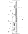
(2)ゲート絶縁層、微結晶半導体層、不純物半導体層の形成
ゲート電極層102と容量電極層104を形成した後、ゲート絶縁層106、微結晶半導体層108、不純物半導体層110を素子基板100上に形成する(図13)。これらの層は、図1乃至図7で説明するプラズマCVD装置を用いることで、各層界面を大気に触れさせることなく連続して積層させることが可能である。
(2) Formation of Gate Insulating Layer, Microcrystalline Semiconductor Layer, and Impurity Semiconductor Layer After forming the
ゲート絶縁層106は、窒化シリコン、酸化シリコン、窒化酸化シリコン、酸化窒化シリコン、窒化アルミニウム、窒化酸化アルミニウムなどの絶縁材料で形成する。まず、図1で示すような構成の処理室にゲート電極層102と容量電極層104が形成された素子基板100を搬送する。そして、該処理室にヘリウムを含む反応性気体を供給し、処理室内の圧力を大気圧若しくは準大気圧に保持しつつ、大気圧若しくは準大気圧においてマイクロ波電力の供給により生成されるプラズマによりゲート絶縁層106の形成を行う。なお、処理室の内側には、窒化シリコン膜又は酸化シリコン膜などゲート絶縁層106と同じ種類若しくは類似する種類の膜をコーティングしておいても良い。それにより、処理室内壁からの脱ガスの割合が低減し、金属不純物などの汚染を防ぐことができる。
The
このように作製されるゲート絶縁層106としては、例えば、ゲート電極層102及び容量電極層104上に第1ゲート絶縁層106aとして窒化シリコン層(又は窒化酸化シリコン層)を設け、その上に第2ゲート絶縁層106bとして酸化シリコン層(又は酸化窒化シリコン層)を設ける。このようにゲート絶縁層106を複数の層で形成することで、複数の機能をゲート絶縁層106に付与することができる。すなわち、第1ゲート絶縁層106aとして窒化シリコン層(又は窒化酸化シリコン層)を設けることで、素子基板100からの不純物拡散を防止し、ゲート電極層102などの酸化防止を図ることができる。また、ゲート電極層102としてアルミニウムを使用する場合には、アルミニウムのヒロックを防止することができる。第2ゲート絶縁層106bとして酸化シリコン層(又は酸化窒化シリコン層)を設けることで、半導体層との密着性を高め、第1ゲート絶縁層106aの応力歪みの影響を緩和する。第1ゲート絶縁層106aは10nm〜100nm、第2ゲート絶縁層106bは50nm〜150nmの厚さで形成することが好ましい。
As the
なお、酸化窒化シリコン膜とは、窒素よりも酸素の含有量が多いものであって、例えば濃度範囲として酸素が55〜65原子%、窒素が1〜20原子%、Siが25〜35原子%、水素(及び/又はOH基)が0.1〜10原子%の範囲で含まれるものをいう。また、窒化酸化シリコン膜とは、その組成として酸素よりも窒素の含有量が多いものであって、例えば濃度範囲として酸素が15〜30原子%、窒素が20〜35原子%、Siが25〜35原子%、水素(及び/又はOH基)が15〜25原子%の範囲で含まれるものをいう。 Note that the silicon oxynitride film has a higher oxygen content than nitrogen. For example, the concentration range is oxygen of 55 to 65 atomic%, nitrogen of 1 to 20 atomic%, and Si of 25 to 35 atomic%. , Hydrogen (and / or OH group) is contained in the range of 0.1 to 10 atomic%. The silicon nitride oxide film has a nitrogen content higher than that of oxygen as a composition. For example, the concentration ranges from 15 to 30 atomic% for oxygen, 20 to 35 atomic% for nitrogen, and 25 to 25 for Si. 35 atom%, and hydrogen (and / or OH group) means what is contained in the range of 15 to 25 atom%.
微結晶半導体層108は、処理室内に載置された素子基板100のゲート絶縁層106上に形成する。その際、処理室にヘリウムを含む反応性気体を供給し、処理室内の圧力を大気圧若しくは準大気圧に保持しつつ、並置された導波管で挟まれた空間にマイクロ波を供給してプラズマを生成させる。反応性気体には、水素と水素化珪素気体若しくはハロゲン化珪素気体とが含まれる。
The
微結晶半導体層108は反応性気体に含まれる水素化珪素気体であるシランをマイクロ波(代表的には2.45GHz)の電磁エネルギーによりプラズマ化して、反応生成物を堆積させることにより形成される。代表的な水素化珪素気体としては、SiH4若しくはSi2H6である。その他、ハロゲン化珪素気体若しくはハロゲン水素化珪素気体としてSiH2Cl2、SiHCl3、SiCl4、SiF4などを用いることができる。基板の加熱温度は100℃から400℃(好ましくは200℃から350℃)とすれば良い。微結晶半導体層108の厚さは50nm〜500nm(好ましくは100nm〜250nm)の厚さとすれば良い。なお、処理室の内側には、微結晶半導体層108と同じ種類若しくは類似する種類の膜をコーティングしておいても良い。微結晶半導体層108をシリコンで形成する場合、シリコン膜などをコーティングする。それにより、処理室内壁からの脱ガスの割合が低減し、金属をはじめとする不純物などの汚染を防ぐことができる。また、プラズマを生成する前に、微結晶半導体層の半導体材料ガス、例えばSiH4ガスを流して処理室中の残留酸素、水分等と反応させて、清浄度を高める処置を行うことが望ましい。
The
この水素化珪素気体などを、希釈ガスで希釈して用いることで微結晶の形成を容易なものとすることができる。希釈ガスには、水素、希ガス(ヘリウム、アルゴン、クリプトン、ネオン)、及びハロゲン気体(フッ素、塩素など)のいずれか一、又はこれらを組み合わせて用いることができ、さらに希ガスであるヘリウム、アルゴン、クリプトン、ネオンは複数組み合わせて用いることもできる。希釈率は10倍〜2000倍の範囲で半導体材料ガスを希釈することが好ましい。プラズマを生成する圧力は、大気圧若しくは準大気圧(1×10²Pa以上1×10⁵Pa以下)で行えば良い。このような圧力でプラズマを生成すると、気相中でラジカル反応が進み、微結晶半導体層における表面反応と相まって成膜速度が向上する。また、気相中でのラジカル反応により微結晶核が生成されることにより、初期段階であるゲート絶縁層106上の被形成面から微結晶性の層を堆積することができる。すなわち、微結晶半導体層108の堆積初期段階において非晶質層が形成されてしまうことを極力防ぐことが可能となる。成膜中に、マイクロ波を1kHz〜100kHzのパルス放電にすることで、気相中でのラジカル反応は制御され気相中で粒子が生成されるなどの異常成長を抑えることができ、好ましい。このように形成される微結晶半導体層は、従来と比較して、50倍程度の堆積速度を達成することができる。
The formation of microcrystals can be facilitated by using the silicon hydride gas diluted with a diluent gas. As the dilution gas, any one of hydrogen, rare gas (helium, argon, krypton, neon), and halogen gas (fluorine, chlorine, etc.) or a combination thereof can be used. Argon, krypton, and neon can be used in combination. It is preferable to dilute the semiconductor material gas in a dilution rate range of 10 to 2000 times. The pressure for generating plasma may be atmospheric pressure or quasi-atmospheric pressure (1 × 10 2 Pa to 1 × 10 5 Pa). When plasma is generated at such a pressure, radical reaction proceeds in the gas phase, and the film formation rate is improved in combination with surface reaction in the microcrystalline semiconductor layer. Further, microcrystalline nuclei are generated by a radical reaction in a gas phase, whereby a microcrystalline layer can be deposited from a formation surface over the
プラズマを生成するためには1GHz〜5GHz、代表的には2.45GHzの電磁波を供給すれば良い。基板加熱温度は500℃以下が好ましく、100℃〜400℃の基板加熱温度が推奨される。また、半導体材料ガス中にCH4、C2H6などの炭素の水素化物、GeH4、GeF4などの水素化ゲルマニウム、フッ化ゲルマニウムを混合して、エネルギーバンド幅を1.5〜2.4eV、若しくは0.9〜1.1eVに調節しても良い。微結晶半導体層を構成するシリコンに、炭素又はゲルマニウムを加えるとTFTの温度特性を変えることができる。 In order to generate plasma, an electromagnetic wave of 1 GHz to 5 GHz, typically 2.45 GHz may be supplied. The substrate heating temperature is preferably 500 ° C. or lower, and a substrate heating temperature of 100 ° C. to 400 ° C. is recommended. Further, carbon hydride such as CH 4 and C 2 H 6 , germanium hydride such as GeH 4 and GeF 4 , and germanium fluoride are mixed in the semiconductor material gas, so that the energy bandwidth is 1.5-2. You may adjust to 4 eV or 0.9-1.1 eV. When carbon or germanium is added to silicon forming the microcrystalline semiconductor layer, the temperature characteristics of the TFT can be changed.
不純物半導体層(不純物を有する半導体層)110は、価電子制御を目的とした一導電型不純物が添加されている。不純物半導体層110をn型とする場合にはリン又は砒素が添加され、p型の場合には硼素が添加される。不純物半導体層110は非晶質半導体又は微結晶半導体で構成される。
The impurity semiconductor layer (semiconductor layer having an impurity) 110 is added with one conductivity type impurity for the purpose of valence electron control. Phosphorus or arsenic is added when the
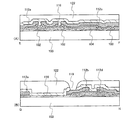
(3)半導体層の加工
素子基板100上に形成された微結晶半導体層108と不純物半導体層110は所定のパターンにエッチング加工される。表示装置の画素領域においては、ゲート電極層102と少なくとも一部、又は全部が重畳するように微結晶半導体層108及び不純物半導体層110をエッチング加工する(図9、図14参照)。このような構造とすることで、TFTのチャネル部の遮光を行うことができ、光の影響を受けることがなく、ゲート電圧を微結晶半導体層108に均一に作用させることができる。微結晶半導体層108及び不純物半導体層110の端部はテーパ状に加工することで、この上層に形成する配線層の段差被覆性を改善し、また半導体層の端部を流れるリーク電流を低減する効果がある。なお、ゲート電極層102及び容量電極層104と、後の工程で作製される配線層との交差部に相当する位置に、ゲート電極層102及び容量電極層104に重ねて半導体層109を設けておくことで、当該交差部における配線層の段差被覆性を改善することができる(図9参照)。半導体層109は、微結晶半導体層108と同じように形成することができる。
(3) Processing of semiconductor layer The
(4)配線層と保護層の形成
ゲート電極層102と交差する方向に延びた配線層及び保護絶縁層116を形成する(図10、図15参照)。配線層は、TFTのソース若しくはドレイン側の電位が付与される配線層112a、画素電極と接続しTFTのドレイン若しくはソース側の電位が付与される配線層112b、容量電極層112cを有している。
(4) Formation of wiring layer and protective layer A wiring layer and a protective
配線層112a、配線層112b、容量電極層112cは、アルミニウム、若しくは銅、耐熱性向上元素若しくはヒロック防止元素(シリコン、チタン、ネオジム、スカンジウムなど)が添加されたアルミニウムを用いて形成することが好ましい。アルミニウムなどをスパッタリング法若しくは蒸着法で形成し、フォトリソグラフィーにより所定のレジストマスクを形成し、エッチングを行うことにより形成される。エッチングはドライエッチング又はウエットエッチングにより行うことができる。このとき作製したレジストマスクを利用して、不純物半導体層110をエッチングする。このエッチングにより微結晶半導体層108の一部は食刻されても良い。配線層112aと配線層112bは、不純物半導体層110と接し、微結晶半導体層108上で離間している。配線層112aと配線層112bの間にある不純物半導体層110をエッチングで除去することにより、TFTのチャネル形成領域が形成される。
The
また配線層112a、配線層112b、容量電極層112cは、銀、銅などの導電性ナノペーストを用いてスクリーン印刷法、インクジェット法、ナノインプリント法を用いて形成しても良い。
Further, the
配線層112a、配線層112b、容量電極層112cは上述のアルミニウム、銅などで形成すれば良いが、下地との密着性向上と拡散を防ぐバリア層として機能する導電性材料を組み合わせた積層構造としても良い。例えば、バリア層として機能する第1導電層113をモリブデン、クロム、チタン、タンタル、窒化チタン等の高融点金属で形成し、第2導電層114を上述のアルミニウム等で形成し、第3導電層115を第1導電層113と同等の高融点金属で形成することができる。
The
保護絶縁層116は、微結晶半導体層108、配線層112a、配線層112b、容量電極層112cなどを被覆するように形成する。保護絶縁層116は、窒化シリコン、窒化酸化シリコンで形成することが好ましい。保護絶縁層116には配線層112bを開口するコンタクトホール117、容量電極層112cを開口するコンタクトホール118を形成する。
The protective
(5)画素電極の形成
画素電極120を保護絶縁層116上に形成する(図11、図16)。画素電極120はコンタクトホール117で配線層112bと、コンタクトホール118で容量電極層112cと接続する。画素電極120は酸化インジウムスズ、酸化亜鉛、酸化スズなどの透明電極材料で形成する。また有機導電性材料で形成しても良い。
(5) Formation of pixel electrode The
画素電極120にはスリットを設けることで液晶の配向を制御することができる。このような構成は、VA(Vertical Alignment)型液晶において適用される。VA型液晶とは、液晶パネルの液晶分子の配列を制御する方式の一種である。VA型液晶は、電圧が印加されていないときにパネル面に対して液晶分子が垂直方向を向く方式である。素子基板100に対向基板を貼り合わせ、その間に液晶層を設けることで液晶表示装置を完成させることができる。
The alignment of the liquid crystal can be controlled by providing a slit in the
このようにして、素子基板100上にTFTとそれに接続する画素電極120、及び保持容量部が形成される。本形態によれば、TFTのチャネルが微結晶半導体で形成されることにより、TFTのしきい値電圧の変動が抑えられ、表示装置の動作安定性を確保することができる。微結晶半導体層はプラズマCVD法により作製可能であり、ポリシリコンのようにレーザ結晶化のような工程が必要ないので生産性を損なうことがない。
In this manner, the TFT, the
(実施の形態2)
本実施の形態ではVA(Vertical Alignment)型液晶であって、画素(ピクセル)をいくつかの領域(サブピクセル)に分けた所謂マルチドメイン設計が考慮された液晶パネルの画素について例示する。図17は、その画素の平面図を示し、当該図中に示すC−D切断線に対応する断面図を図18に示す。
(Embodiment 2)
In this embodiment, an example of a pixel of a liquid crystal panel which is a VA (Vertical Alignment) type liquid crystal and which considers a so-called multi-domain design in which a pixel (pixel) is divided into several regions (sub-pixels) will be described. FIG. 17 is a plan view of the pixel, and FIG. 18 is a cross-sectional view corresponding to the CD cut line shown in the figure.
素子基板100、ゲート電極層102、容量電極層104、ゲート絶縁層106、微結晶半導体層108、不純物半導体層110、配線層112a、112b、容量電極層112cの構成は実施の形態1と同様である。保護絶縁層116の上には層間絶縁層122が形成され、それらを貫通するコンタクトホール117が形成されている。層間絶縁層122は酸化シリコンなどの無機絶縁材料、ポリイミド、アクリルなどで代表される有機絶縁材料で形成される。
The structure of the
画素電極120は層間絶縁層122上に設けられている。画素電極120には液晶の配向を制御するためにスリットが設けられている。画素電極120に隣接する画素電極121は、画素電極120に接続するTFTと同じタイミングでゲート電位が印加される別のTFTと接続している。本形態では1画素(ピクセル)は、画素電極120と画素電極121により構成されている。すなわち、画素電極120と画素電極121はそれぞれ画素のサブピクセルを構成する。この場合、容量電極層104と容量電極層105との電位を異ならせることで、画素電極120と画素電極121との電位を異ならせることができる。すなわち、容量電極層104と容量電極層105との電位を個別に制御することにより液晶の配向を精密に制御して視野角を広げることができる。
The
図19は素子基板100と対向基板101を重ね合わせ、液晶を注入した状態を示している。対向基板101においてスペーサ136が形成される位置には、遮光層126、第1着色層128、第2着色層130、第3着色層132、対向電極134が形成されている。この構造により、液晶の配向を制御するための突起状のリブ138とスペーサ136の高さを異ならせている。画素電極120と対向電極134には配向膜124が形成されている。この間に液晶層140が形成されている。
FIG. 19 shows a state in which the
本形態によれば、TFTのチャネルが微結晶半導体で形成されることにより、TFTのしきい値電圧の変動が抑えられ、マルチドメイン型の液晶表示装置の動作安定性を確保することができる。微結晶半導体層はプラズマCVD法により作製可能であり、ポリシリコンのようにレーザ結晶化のような工程が必要ないので生産性を損なうことがない。 According to this embodiment, since the TFT channel is formed of a microcrystalline semiconductor, variation in the threshold voltage of the TFT can be suppressed, and the operation stability of the multi-domain liquid crystal display device can be ensured. The microcrystalline semiconductor layer can be manufactured by a plasma CVD method and does not require a process such as laser crystallization like polysilicon, so that productivity is not impaired.
(実施の形態3)
微結晶半導体層でチャネルを形成するTFTにより構成される表示装置の一製造工程を、図面を参照して説明する。本形態では画素に発光素子を設けた構成の表示装置について示す。図20、図21、図22、図23は画素の平面図を示し、断面図を図24、図25、図26、図27、図28、図29、図30に示す。図24、図25、図26、図27、図28、図29、図30において、平面図に示すE−F切断線に対応する断面図をそれぞれ(A)に、G−H切断線に対応する断面図をそれぞれ(B)に示す。以下の説明ではこれら平面図と断面図を適宜参照しながら説明する。
(Embodiment 3)
One manufacturing process of a display device including a TFT in which a channel is formed using a microcrystalline semiconductor layer is described with reference to drawings. In this embodiment mode, a display device in which a pixel is provided with a light-emitting element is described. 20, FIG. 21, FIG. 22, and FIG. 23 are plan views of the pixels, and cross-sectional views are shown in FIG. 24, FIG. 25, FIG. 26, FIG. 24, 25, 26, 27, 28, 29, and 30, (A) is a cross-sectional view corresponding to the EF cutting line shown in the plan view, and (G) is a GH cutting line. Sectional views to be shown are shown in FIG. The following description will be given with reference to these plan views and cross-sectional views as appropriate.
(1)ゲート電極及び容量電極の形成
TFTが作製される素子基板100は、ガラス基板等の絶縁表面を有する平板状の基板が適用される。素子基板100には、ゲート電極層102、ゲート電極層103、容量電極層104が形成される(図20、図24(A)(B)参照)。
(1) Formation of Gate Electrode and Capacitance Electrode A flat substrate having an insulating surface such as a glass substrate is applied to the
(2)ゲート絶縁層、微結晶半導体層の形成
ゲート電極層102、ゲート電極層103、容量電極層104を形成した後、ゲート絶縁層106、微結晶半導体層108を素子基板100上に形成する(図25(A)(B)参照)。これらの層は、図1乃至図7で説明するプラズマCVD装置を用いることで、各層界面を大気に触れさせることなく連続して積層させることが可能である。成膜方法については実施の形態1と同様である。
(2) Formation of Gate Insulating Layer and Microcrystalline Semiconductor Layer After forming the
(3)半導体層の加工
素子基板100上に形成された微結晶半導体層108は所定のパターンにエッチング加工する。その後チャネル保護絶縁層111a、チャネル保護絶縁層111bを形成する。(図21、図26(A)(B)参照)。チャネル保護絶縁層111aは微結晶半導体層108aがゲート電極層102と重なるように形成し、チャネル保護絶縁層111bは微結晶半導体層108bがゲート電極層103と重なるように形成する。チャネル保護絶縁層111a、チャネル保護絶縁層111bは微結晶半導体層108a、微結晶半導体層108bの酸化を防止するために窒化シリコンで形成することが好ましい。ゲート絶縁層106には下層のゲート電極層103を露出させるコンタクトホール107を形成する。
(3) Processing of semiconductor layer The
(4)不純物半導体層と配線層の形成
不純物半導体層110aと配線層112a、不純物半導体層110bと配線層112b、不純物半導体層110cと容量電極層112c、及び不純物半導体層110dと容量電極層112dは同じレジストマスクパターンを使って形成する(図22、図27(A)(B)参照)。配線層112aはゲート電極層102と交差する配線でありソース線若しくはデータ線とも呼ばれる。配線層112bは画素電極とトランジスタを接続する配線である。容量電極層112cは画素に設けられる2つのトランジスタを接続する配線であり、コンタクトホール107でゲート電極層103と接続する。また、容量電極層112cと容量電極層104との重畳領域にはゲート絶縁層106が介在し、この領域に保持容量が形成される。
(4) Formation of impurity semiconductor layer and wiring layer The
(5)保護絶縁層と層間絶縁層の形成
配線層112a、112bと容量電極層112c、112dの上層に保護絶縁層116と層間絶縁層122を形成する。そして、配線層112bを開口するコンタクトホール119を形成する(図28(A)(B)参照)。
(5) Formation of protective insulating layer and interlayer insulating layer The protective
(6)画素電極と隔壁絶縁層の形成
画素電極120を層間絶縁層122上に形成する(図23、図29(A)(B)参照)。画素電極120はコンタクトホール119で配線層112bと接続する。画素電極120上に絶縁層123を形成する。絶縁層123は画素電極120の周辺を覆い内側を開口する絶縁層であり、隣接する画素を区分けしている。
(6) Formation of Pixel Electrode and Partition Insulating Layer The
(7)EL層と対向電極層の形成
その後、EL層142と対向電極層144を形成する(図30(A)(B)参照)。EL層142はエレクトロルミネセンス材料を含んで形成される層である。EL層142を画素電極120と対向電極層144で挟むことにより発光素子が形成され、当該発光素子が各画素に設けられることとなる。画素電極120を非透光性の電極で形成し、対向電極層144を透光性の電極とすることにより、発光素子からの光が対向電極層144側に出るトップエミッション型の表示装置を構成することができる。また、画素電極120を透光性の電極とし、対向電極層144を非透光性の電極とすることにより、発光素子からの光が画素電極120側に出るボトムエミッション型の表示装置を構成することができる。
(7) Formation of EL layer and counter electrode layer Then, an
本形態によれば、TFTのチャネルが微結晶半導体で形成されることにより、TFTのしきい値電圧の変動が抑えられ、発光素子を各画素に設ける表示装置の動作安定性を確保することができる。微結晶半導体層はプラズマCVD法により作製可能であり、ポリシリコンのようにレーザ結晶化のような工程が必要ないので生産性を損なうことがない。レーザ結晶化は結晶化斑が生じやすい場合があり、それがTFT特性に影響を与え発光素子の輝度バラツキの原因となる。しかし、本形態によれば微結晶半導体層を均一に形成することができるので、発光素子の輝度バラツキによる表示斑の影響を受けにくいという特性がある。 According to this embodiment, since the TFT channel is formed of a microcrystalline semiconductor, variation in the threshold voltage of the TFT can be suppressed, and operation stability of the display device in which the light emitting element is provided in each pixel can be ensured. it can. The microcrystalline semiconductor layer can be manufactured by a plasma CVD method and does not require a process such as laser crystallization like polysilicon, so that productivity is not impaired. Laser crystallization may cause crystallization spots, which affects TFT characteristics and causes variations in luminance of light emitting elements. However, according to this embodiment, since the microcrystalline semiconductor layer can be formed uniformly, there is a characteristic that the microcrystalline semiconductor layer is hardly affected by display unevenness due to luminance variation of the light-emitting element.
(実施の形態4)
実施の形態1乃至3で例示される表示装置は様々な用途に適用することができる。図31はその一例であり、インターネットに代表される情報ネットワークに接続される表示装置の一例を示す。この表示装置200は微結晶半導体層でチャネルが形成されるTFTにより画素が構成される表示パネル201を有している。表示装置200は、例えばネットワーク接続アダプタ206を介して通信ネットワークと接続される。表示装置200は操作ボード203によって表示画像等の選択をすることができる。操作ボード203は入力部205を有する。入力部205はキーボードの他、マウスなどのポインティングデバイス、図示するようなペン204により情報を入力する方式としても良い。また音声入力部207を設けてペン入力や音声認識機能といった直感的な操作方式とすることもできる。操作ボード203は赤外線若しくは電波を使った無線通信方式202により表示装置200と接続可能とされる。送受信される情報を表示装置200に表示させながら操作ボード203により情報の受信及び送信を行うことができる。微結晶半導体層でチャネルが形成されるTFTにより画素が構成される表示パネル201を有しているので、高精細画面を構成することが可能であり、情報密度の高い画像を自在に取捨選択して楽しむことができる。
(Embodiment 4)
The display devices described in
100 素子基板
101 対向基板
102、103 ゲート電極層
104、105 容量電極層
106 ゲート絶縁層
107 コンタクトホール
108 微結晶半導体層
109 半導体層
110 不純物半導体層
113〜115 導電層
116 保護絶縁層
117〜119 コンタクトホール
120、121 画素電極
122 層間絶縁層
123 絶縁層
124 配向膜
126 遮光層
128〜132 着色層
134 対向電極
136 スペーサ
138 リブ
140 液晶層
100
Claims (8)
前記サセプタの上部に、互いに間隔をおいて並んで設けられた複数の導波管と、
隣り合う前記導波管同士で挟まれた空間に設けられたプラズマ発生器と、
を有する処理室を有し、
前記処理室内の圧力を1×10 2 Pa以上1×10 5 Pa以下に保持しつつ、前記プラズマ発生器を動作させ、前記空間においてプラズマを生成することで、前記被処理体に微結晶半導体層を成膜することを特徴とするプラズマCVD装置。 A susceptor on which an object is placed;
A plurality of waveguides provided on top of the susceptor and spaced apart from each other;
A plasma generator provided in a space sandwiched between the adjacent waveguides;
A processing chamber having
While maintaining the pressure in the processing chamber at 1 × 10 2 Pa or more and 1 × 10 5 Pa or less, the plasma generator is operated to generate plasma in the space, whereby a microcrystalline semiconductor layer is formed on the object to be processed. A plasma CVD apparatus characterized by forming a film.
前記サセプタの上部に、互いに間隔をおいて並んで設けられた複数の導波管と、
隣り合う前記導波管同士で挟まれた空間に設けられたプラズマ発生器と、
を有する処理室を有し、
複数の前記導波管は前記被処理体の被処理面に対して平行な方向に延びた形状であり、
前記空間は細溝状であり、
前記処理室内の圧力を1×10 2 Pa以上1×10 5 Pa以下に保持しつつ、前記プラズマ発生器を動作させ、前記空間においてプラズマを生成することで、前記被処理体に微結晶半導体層を成膜することを特徴とするプラズマCVD装置。 A susceptor on which an object is placed;
A plurality of waveguides provided on top of the susceptor and spaced apart from each other;
A plasma generator provided in a space sandwiched between the adjacent waveguides;
A processing chamber having
The plurality of waveguides have a shape extending in a direction parallel to the surface to be processed of the object to be processed,
The space has a narrow groove shape,
While maintaining the pressure in the processing chamber at 1 × 10 2 Pa or more and 1 × 10 5 Pa or less, the plasma generator is operated to generate plasma in the space, whereby a microcrystalline semiconductor layer is formed on the object to be processed. A plasma CVD apparatus characterized by forming a film.
複数の前記導波管のそれぞれの側面にはスリットが設けられ、
隣り合う前記導波管同士において、前記スリット同士が対向するように設けられ、
前記スリットからマイクロ波が漏洩して前記プラズマを生成することを特徴とするプラズマCVD装置。 In claim 1 or claim 2,
A slit is provided on each side surface of the plurality of waveguides,
In the adjacent waveguides, the slits are provided to face each other,
A plasma CVD apparatus characterized in that microwaves leak from the slit to generate the plasma.
前記スリットは誘電体板により塞がれていることを特徴とするプラズマCVD装置。 In claim 3,
The plasma CVD apparatus, wherein the slit is closed by a dielectric plate.
前記処理室は、前記サセプタと前記導波管と間に2つのガス供給ノズルを有し、
前記ガス供給ノズルの一方からは希ガスを供給し、他方からは成膜用のガスを供給することを特徴とするプラズマCVD装置。 In any one of Claims 1 thru | or 4,
The processing chamber has two gas supply nozzles between the susceptor and the waveguide,
A plasma CVD apparatus, wherein a rare gas is supplied from one of the gas supply nozzles and a film forming gas is supplied from the other.
複数の前記導波管同士は、2mm以上10mm以下の間隔をおいて並んで設けられていることを特徴とするプラズマCVD装置。 In any one of Claims 1 thru | or 5 ,
The plasma CVD apparatus, wherein the plurality of waveguides are provided side by side with an interval of 2 mm to 10 mm.
前記処理室内の圧力を1×10 2 Pa以上1×10 5 Pa以下に保持しつつ、前記プラズマ発生器を動作させ、前記空間においてプラズマを生成することで、前記被処理基板上に微結晶半導体層を形成することを特徴とする表示装置の作製方法。 A susceptor on which the object to be processed is placed; a plurality of waveguides provided side by side at intervals; and a plasma generator provided in a space sandwiched between the adjacent waveguides. In the processing chamber, a substrate to be processed is prepared on the susceptor,
A microcrystalline semiconductor is formed on the substrate to be processed by operating the plasma generator and generating plasma in the space while maintaining the pressure in the processing chamber at 1 × 10 2 Pa or more and 1 × 10 5 Pa or less. A method for manufacturing a display device, comprising forming a layer.
前記プラズマは電子密度が1×1011cm−3以上1×1013cm−3以下であり、電子温度が0.2eV以上2.0eV以下であることを特徴とする表示装置の作製方法。 In claim 7 ,
The plasma has an electron density of 1 × 10 11 cm −3 to 1 × 10 13 cm −3 and an electron temperature of 0.2 eV to 2.0 eV.
Priority Applications (1)
| Application Number | Priority Date | Filing Date | Title |
|---|---|---|---|
| JP2008172141A JP5216446B2 (en) | 2007-07-27 | 2008-07-01 | Plasma CVD apparatus and display device manufacturing method |
Applications Claiming Priority (3)
| Application Number | Priority Date | Filing Date | Title |
|---|---|---|---|
| JP2007196189 | 2007-07-27 | ||
| JP2007196189 | 2007-07-27 | ||
| JP2008172141A JP5216446B2 (en) | 2007-07-27 | 2008-07-01 | Plasma CVD apparatus and display device manufacturing method |
Publications (3)
| Publication Number | Publication Date |
|---|---|
| JP2009054996A JP2009054996A (en) | 2009-03-12 |
| JP2009054996A5 JP2009054996A5 (en) | 2011-08-04 |
| JP5216446B2 true JP5216446B2 (en) | 2013-06-19 |
Family
ID=40295760
Family Applications (1)
| Application Number | Title | Priority Date | Filing Date |
|---|---|---|---|
| JP2008172141A Expired - Fee Related JP5216446B2 (en) | 2007-07-27 | 2008-07-01 | Plasma CVD apparatus and display device manufacturing method |
Country Status (3)
| Country | Link |
|---|---|
| US (1) | US8178398B2 (en) |
| JP (1) | JP5216446B2 (en) |
| KR (1) | KR101512758B1 (en) |
Families Citing this family (12)
| Publication number | Priority date | Publication date | Assignee | Title |
|---|---|---|---|---|
| JP4719184B2 (en) * | 2007-06-01 | 2011-07-06 | 株式会社サイアン | Atmospheric pressure plasma generator and work processing apparatus using the same |
| JP5058084B2 (en) * | 2007-07-27 | 2012-10-24 | 株式会社半導体エネルギー研究所 | Method for manufacturing photoelectric conversion device and microwave plasma CVD apparatus |
| JP5572307B2 (en) | 2007-12-28 | 2014-08-13 | 株式会社半導体エネルギー研究所 | Method for manufacturing photoelectric conversion device |
| US8803245B2 (en) * | 2008-06-30 | 2014-08-12 | Mcafee, Inc. | Method of forming stacked trench contacts and structures formed thereby |
| JP5632654B2 (en) * | 2009-05-29 | 2014-11-26 | 株式会社半導体エネルギー研究所 | Display device |
| JP5752447B2 (en) * | 2010-03-15 | 2015-07-22 | 株式会社半導体エネルギー研究所 | Semiconductor device |
| US8440548B2 (en) | 2010-08-06 | 2013-05-14 | Semiconductor Energy Laboratory Co., Ltd. | Manufacturing method of microcrystalline silicon film and manufacturing method of thin film transistor |
| US9553195B2 (en) * | 2011-06-30 | 2017-01-24 | Applied Materials, Inc. | Method of IGZO and ZNO TFT fabrication with PECVD SiO2 passivation |
| US20120175667A1 (en) * | 2011-10-03 | 2012-07-12 | Golle Aaron J | Led light disposed on a flexible substrate and connected with a printed 3d conductor |
| KR102377794B1 (en) * | 2015-07-06 | 2022-03-23 | 엘지전자 주식회사 | Display device using semiconductor light emitting device and method for manufacturing |
| JP6899693B2 (en) * | 2017-04-14 | 2021-07-07 | 東京エレクトロン株式会社 | Plasma processing equipment and control method |
| JP2023033720A (en) * | 2021-08-30 | 2023-03-13 | 東京エレクトロン株式会社 | Deposition method and deposition device |
Family Cites Families (52)
| Publication number | Priority date | Publication date | Assignee | Title |
|---|---|---|---|---|
| JPS6029295B2 (en) * | 1979-08-16 | 1985-07-10 | 舜平 山崎 | Non-single crystal film formation method |
| US5091334A (en) * | 1980-03-03 | 1992-02-25 | Semiconductor Energy Laboratory Co., Ltd. | Semiconductor device |
| JPS56122123A (en) * | 1980-03-03 | 1981-09-25 | Shunpei Yamazaki | Semiamorphous semiconductor |
| JPS5771126A (en) | 1980-10-21 | 1982-05-01 | Semiconductor Energy Lab Co Ltd | Semiamorhous semiconductor |
| JPS5972781A (en) | 1982-10-20 | 1984-04-24 | Semiconductor Energy Lab Co Ltd | Photoelectric conversion semiconductor device |
| JPS61241921A (en) * | 1985-04-19 | 1986-10-28 | Hitachi Ltd | Plasma treatment apparatus |
| JPS6262073A (en) | 1985-09-11 | 1987-03-18 | Ishikawajima Harima Heavy Ind Co Ltd | Device for controlling temperature of poppet valve |
| US4760008A (en) * | 1986-01-24 | 1988-07-26 | Semiconductor Energy Laboratory Co., Ltd. | Electrophotographic photosensitive members and methods for manufacturing the same using microwave radiation in magnetic field |
| US4988642A (en) * | 1988-05-25 | 1991-01-29 | Semiconductor Energy Laboratory Co., Ltd. | Semiconductor device, manufacturing method, and system |
| JPH0253941A (en) | 1988-08-17 | 1990-02-22 | Tsudakoma Corp | Operation apparatus for loom |
| JP2876318B2 (en) * | 1989-01-20 | 1999-03-31 | 三洋電機株式会社 | Thin film formation method |
| US7115902B1 (en) * | 1990-11-20 | 2006-10-03 | Semiconductor Energy Laboratory Co., Ltd. | Electro-optical device and method for manufacturing the same |
| KR950013784B1 (en) * | 1990-11-20 | 1995-11-16 | 가부시키가이샤 한도오따이 에네루기 겐큐쇼 | Field effect trasistor and its making method and tft |
| US5849601A (en) * | 1990-12-25 | 1998-12-15 | Semiconductor Energy Laboratory Co., Ltd. | Electro-optical device and method for manufacturing the same |
| US5514879A (en) * | 1990-11-20 | 1996-05-07 | Semiconductor Energy Laboratory Co., Ltd. | Gate insulated field effect transistors and method of manufacturing the same |
| US7576360B2 (en) * | 1990-12-25 | 2009-08-18 | Semiconductor Energy Laboratory Co., Ltd. | Electro-optical device which comprises thin film transistors and method for manufacturing the same |
| US7098479B1 (en) * | 1990-12-25 | 2006-08-29 | Semiconductor Energy Laboratory Co., Ltd. | Electro-optical device and method for manufacturing the same |
| JPH0613329A (en) * | 1992-06-25 | 1994-01-21 | Canon Inc | Semiconductor device and manufacture thereof |
| US5946587A (en) * | 1992-08-06 | 1999-08-31 | Canon Kabushiki Kaisha | Continuous forming method for functional deposited films |
| US6835523B1 (en) * | 1993-05-09 | 2004-12-28 | Semiconductor Energy Laboratory Co., Ltd. | Apparatus for fabricating coating and method of fabricating the coating |
| US5932302A (en) * | 1993-07-20 | 1999-08-03 | Semiconductor Energy Laboratory Co., Ltd. | Method for fabricating with ultrasonic vibration a carbon coating |
| JPH11103082A (en) | 1997-09-26 | 1999-04-13 | Canon Inc | Photosensor and manufacture thereof |
| JP2000277439A (en) | 1999-03-25 | 2000-10-06 | Kanegafuchi Chem Ind Co Ltd | Plasma cvd method for crystalline silicon thin-film and manufacture of silicon thin-film photoelectric conversion device |
| WO2000074127A1 (en) * | 1999-05-26 | 2000-12-07 | Tokyo Electron Limited | Plasma process device |
| JP2000353666A (en) | 1999-06-11 | 2000-12-19 | Matsushita Electric Ind Co Ltd | Semiconductor thin film and manufacture thereof |
| JP2001313257A (en) * | 2000-04-28 | 2001-11-09 | Mitsubishi Heavy Ind Ltd | Method for producing high quality silicon based thin film |
| JP2002033307A (en) | 2000-07-17 | 2002-01-31 | Shibaura Mechatronics Corp | Plasma generator and plasma treatment equipment provided with the generator |
| JP2002371357A (en) * | 2001-06-14 | 2002-12-26 | Canon Inc | Method for forming silicon-based thin film, silicon-based thin film, semiconductor device, and apparatus for forming silicon-based thin film |
| TW521540B (en) * | 2001-10-03 | 2003-02-21 | Hau-Ran Ni | An ECR plasma reactor system with multiple exciters |
| JP4173679B2 (en) * | 2002-04-09 | 2008-10-29 | エム・イー・エス・アフティ株式会社 | ECR plasma source and ECR plasma apparatus |
| JP2004014958A (en) | 2002-06-11 | 2004-01-15 | Fuji Electric Holdings Co Ltd | Thin film polycrystalline solar cell and manufacturing method therefor |
| JP2004336019A (en) * | 2003-04-18 | 2004-11-25 | Advanced Lcd Technologies Development Center Co Ltd | Film forming method, forming method of semiconductor element, semiconductor element, forming method of indicating device, and indicating device |
| JP4748954B2 (en) | 2003-07-14 | 2011-08-17 | 株式会社半導体エネルギー研究所 | Liquid crystal display |
| TWI336921B (en) * | 2003-07-18 | 2011-02-01 | Semiconductor Energy Lab | Method for manufacturing semiconductor device |
| JP4480968B2 (en) * | 2003-07-18 | 2010-06-16 | 株式会社半導体エネルギー研究所 | Display device |
| US7211454B2 (en) * | 2003-07-25 | 2007-05-01 | Semiconductor Energy Laboratory Co., Ltd. | Manufacturing method of a light emitting device including moving the source of the vapor deposition parallel to the substrate |
| JP2005050905A (en) * | 2003-07-30 | 2005-02-24 | Sharp Corp | Method for manufacturing silicon thin film solar cell |
| KR101130232B1 (en) * | 2003-11-14 | 2012-03-27 | 가부시키가이샤 한도오따이 에네루기 켄큐쇼 | Display device and method for manufacturing the same |
| JP4393844B2 (en) * | 2003-11-19 | 2010-01-06 | 東京エレクトロン株式会社 | Plasma film forming apparatus and plasma film forming method |
| JP4659377B2 (en) | 2004-03-19 | 2011-03-30 | 株式会社 液晶先端技術開発センター | Insulating film formation method |
| JP5013393B2 (en) * | 2005-03-30 | 2012-08-29 | 東京エレクトロン株式会社 | Plasma processing apparatus and method |
| JP2006294422A (en) * | 2005-04-11 | 2006-10-26 | Tokyo Electron Ltd | Plasma treatment apparatus, slot antenna and plasma treatment method |
| TWI408734B (en) * | 2005-04-28 | 2013-09-11 | Semiconductor Energy Lab | Semiconductor device and method for manufacturing the same |
| US7608490B2 (en) * | 2005-06-02 | 2009-10-27 | Semiconductor Energy Laboratory Co., Ltd. | Semiconductor device and manufacturing method thereof |
| JP4597792B2 (en) | 2005-06-27 | 2010-12-15 | 東京エレクトロン株式会社 | Process gas supply structure and plasma processing apparatus |
| JP4777717B2 (en) | 2005-08-10 | 2011-09-21 | 東京エレクトロン株式会社 | Film forming method, plasma processing apparatus, and recording medium |
| US7301215B2 (en) * | 2005-08-22 | 2007-11-27 | Canon Kabushiki Kaisha | Photovoltaic device |
| US7692610B2 (en) * | 2005-11-30 | 2010-04-06 | Semiconductor Energy Laboratory Co., Ltd. | Display device |
| JP5068458B2 (en) * | 2006-01-18 | 2012-11-07 | 東京エレクトロン株式会社 | Plasma processing apparatus and plasma processing method |
| JP4978985B2 (en) * | 2006-03-30 | 2012-07-18 | 東京エレクトロン株式会社 | Plasma processing method |
| JP5364293B2 (en) * | 2007-06-01 | 2013-12-11 | 株式会社半導体エネルギー研究所 | Display device manufacturing method and plasma CVD apparatus |
| US8207010B2 (en) * | 2007-06-05 | 2012-06-26 | Semiconductor Energy Laboratory Co., Ltd. | Method for manufacturing photoelectric conversion device |
-
2008
- 2008-07-01 JP JP2008172141A patent/JP5216446B2/en not_active Expired - Fee Related
- 2008-07-18 US US12/219,244 patent/US8178398B2/en not_active Expired - Fee Related
- 2008-07-21 KR KR1020080070707A patent/KR101512758B1/en not_active Application Discontinuation
Also Published As
| Publication number | Publication date |
|---|---|
| KR20090012094A (en) | 2009-02-02 |
| KR101512758B1 (en) | 2015-04-16 |
| JP2009054996A (en) | 2009-03-12 |
| US20090029498A1 (en) | 2009-01-29 |
| US8178398B2 (en) | 2012-05-15 |
Similar Documents
| Publication | Publication Date | Title |
|---|---|---|
| JP5216446B2 (en) | Plasma CVD apparatus and display device manufacturing method | |
| US8368075B2 (en) | Plasma CVD apparatus | |
| TWI793890B (en) | Liquid crystal display device | |
| TWI447915B (en) | Manufacturing method of semiconductor device | |
| JP5542277B2 (en) | Method for manufacturing microcrystalline semiconductor film and thin film transistor | |
| JP5478380B2 (en) | Plasma deposition system | |
| TWI601188B (en) | Method for manufacturing microcrystalline semiconductor film and method for manufacturing semiconductor device | |
| US7446060B2 (en) | Thin-film forming method using silane and an oxidizing gas | |
| TWI437642B (en) | Method for manufacturing semiconductor device | |
| US8525170B2 (en) | Thin film transistor and manufacturing method thereof | |
| US9935183B2 (en) | Multilayer passivation or etch stop TFT | |
| JP4018625B2 (en) | Multi-stage CVD method for thin film transistors | |
| JP2007221137A (en) | Method of forming silicon layer, and method of manufacturing display substrate using same | |
| KR20090054902A (en) | Method for manufacturing semiconductor device | |
| KR101752646B1 (en) | Method for forming microcrystalline semiconductor film and method for manufacturing thin film transistor | |
| TWI497724B (en) | Thin film transistor and manufacturing method thereof | |
| JP2005252012A (en) | Deposited film forming method, forming method of semiconductor element, semiconductor device and display device | |
| TWM497672U (en) | Reduced zinc showerhead | |
| WO2013132937A1 (en) | Method for manufacturing thin film transistor and method for manufacturing display device | |
| WO2012176410A1 (en) | Method for manufacturing thin film transistor substrate, thin film transistor substrate manufactured by same, and method for manufacturing semiconductor film | |
| JPH104062A (en) | High frequency plasma cvd apparatus |
Legal Events
| Date | Code | Title | Description |
|---|---|---|---|
| A521 | Request for written amendment filed |
Free format text: JAPANESE INTERMEDIATE CODE: A523 Effective date: 20110616 |
|
| A621 | Written request for application examination |
Free format text: JAPANESE INTERMEDIATE CODE: A621 Effective date: 20110616 |
|
| A977 | Report on retrieval |
Free format text: JAPANESE INTERMEDIATE CODE: A971007 Effective date: 20120127 |
|
| A131 | Notification of reasons for refusal |
Free format text: JAPANESE INTERMEDIATE CODE: A131 Effective date: 20130108 |
|
| A521 | Request for written amendment filed |
Free format text: JAPANESE INTERMEDIATE CODE: A523 Effective date: 20130207 |
|
| TRDD | Decision of grant or rejection written | ||
| A01 | Written decision to grant a patent or to grant a registration (utility model) |
Free format text: JAPANESE INTERMEDIATE CODE: A01 Effective date: 20130226 |
|
| A61 | First payment of annual fees (during grant procedure) |
Free format text: JAPANESE INTERMEDIATE CODE: A61 Effective date: 20130304 |
|
| R150 | Certificate of patent or registration of utility model |
Ref document number: 5216446 Country of ref document: JP Free format text: JAPANESE INTERMEDIATE CODE: R150 Free format text: JAPANESE INTERMEDIATE CODE: R150 |
|
| FPAY | Renewal fee payment (event date is renewal date of database) |
Free format text: PAYMENT UNTIL: 20160308 Year of fee payment: 3 |
|
| FPAY | Renewal fee payment (event date is renewal date of database) |
Free format text: PAYMENT UNTIL: 20160308 Year of fee payment: 3 |
|
| R250 | Receipt of annual fees |
Free format text: JAPANESE INTERMEDIATE CODE: R250 |
|
| R250 | Receipt of annual fees |
Free format text: JAPANESE INTERMEDIATE CODE: R250 |
|
| R250 | Receipt of annual fees |
Free format text: JAPANESE INTERMEDIATE CODE: R250 |
|
| R250 | Receipt of annual fees |
Free format text: JAPANESE INTERMEDIATE CODE: R250 |
|
| R250 | Receipt of annual fees |
Free format text: JAPANESE INTERMEDIATE CODE: R250 |
|
| R250 | Receipt of annual fees |
Free format text: JAPANESE INTERMEDIATE CODE: R250 |
|
| LAPS | Cancellation because of no payment of annual fees |