JP5207777B2 - Solid-state imaging device and manufacturing method thereof - Google Patents
Solid-state imaging device and manufacturing method thereof Download PDFInfo
- Publication number
- JP5207777B2 JP5207777B2 JP2008056283A JP2008056283A JP5207777B2 JP 5207777 B2 JP5207777 B2 JP 5207777B2 JP 2008056283 A JP2008056283 A JP 2008056283A JP 2008056283 A JP2008056283 A JP 2008056283A JP 5207777 B2 JP5207777 B2 JP 5207777B2
- Authority
- JP
- Japan
- Prior art keywords
- vertical transfer
- solid
- imaging device
- state imaging
- insulating film
- Prior art date
- Legal status (The legal status is an assumption and is not a legal conclusion. Google has not performed a legal analysis and makes no representation as to the accuracy of the status listed.)
- Expired - Fee Related
Links
- 238000003384 imaging method Methods 0.000 title claims description 132
- 238000004519 manufacturing process Methods 0.000 title claims description 33
- 229910052751 metal Inorganic materials 0.000 claims description 78
- 239000002184 metal Substances 0.000 claims description 78
- 239000011229 interlayer Substances 0.000 claims description 49
- 239000000758 substrate Substances 0.000 claims description 37
- 238000006243 chemical reaction Methods 0.000 claims description 36
- 239000004065 semiconductor Substances 0.000 claims description 35
- 238000000034 method Methods 0.000 claims description 25
- 239000000463 material Substances 0.000 claims description 24
- 238000005530 etching Methods 0.000 claims description 17
- 239000011159 matrix material Substances 0.000 claims description 12
- 229910052581 Si3N4 Inorganic materials 0.000 claims description 8
- HQVNEWCFYHHQES-UHFFFAOYSA-N silicon nitride Chemical compound N12[Si]34N5[Si]62N3[Si]51N64 HQVNEWCFYHHQES-UHFFFAOYSA-N 0.000 claims description 8
- 238000011144 upstream manufacturing Methods 0.000 claims description 6
- 238000012986 modification Methods 0.000 description 32
- 230000004048 modification Effects 0.000 description 29
- 238000000926 separation method Methods 0.000 description 12
- 239000010410 layer Substances 0.000 description 10
- 230000035945 sensitivity Effects 0.000 description 10
- 239000011347 resin Substances 0.000 description 9
- 229920005989 resin Polymers 0.000 description 9
- 229910052782 aluminium Inorganic materials 0.000 description 6
- XAGFODPZIPBFFR-UHFFFAOYSA-N aluminium Chemical compound [Al] XAGFODPZIPBFFR-UHFFFAOYSA-N 0.000 description 6
- 150000004767 nitrides Chemical class 0.000 description 6
- 229910021332 silicide Inorganic materials 0.000 description 6
- FVBUAEGBCNSCDD-UHFFFAOYSA-N silicide(4-) Chemical compound [Si-4] FVBUAEGBCNSCDD-UHFFFAOYSA-N 0.000 description 6
- WFKWXMTUELFFGS-UHFFFAOYSA-N tungsten Chemical compound [W] WFKWXMTUELFFGS-UHFFFAOYSA-N 0.000 description 6
- 229910052721 tungsten Inorganic materials 0.000 description 6
- 239000010937 tungsten Substances 0.000 description 6
- VYPSYNLAJGMNEJ-UHFFFAOYSA-N Silicium dioxide Chemical compound O=[Si]=O VYPSYNLAJGMNEJ-UHFFFAOYSA-N 0.000 description 5
- 229910052814 silicon oxide Inorganic materials 0.000 description 5
- 230000007547 defect Effects 0.000 description 2
- 238000010586 diagram Methods 0.000 description 2
- 238000000059 patterning Methods 0.000 description 2
- 229920002120 photoresistant polymer Polymers 0.000 description 2
- XUIMIQQOPSSXEZ-UHFFFAOYSA-N Silicon Chemical compound [Si] XUIMIQQOPSSXEZ-UHFFFAOYSA-N 0.000 description 1
- 230000005540 biological transmission Effects 0.000 description 1
- 230000015572 biosynthetic process Effects 0.000 description 1
- 239000005380 borophosphosilicate glass Substances 0.000 description 1
- 230000000052 comparative effect Effects 0.000 description 1
- 238000011109 contamination Methods 0.000 description 1
- 230000006866 deterioration Effects 0.000 description 1
- 230000000694 effects Effects 0.000 description 1
- 230000005684 electric field Effects 0.000 description 1
- 238000009413 insulation Methods 0.000 description 1
- 238000002955 isolation Methods 0.000 description 1
- 230000002093 peripheral effect Effects 0.000 description 1
- 229910021420 polycrystalline silicon Inorganic materials 0.000 description 1
- 229920005591 polysilicon Polymers 0.000 description 1
- 229910052710 silicon Inorganic materials 0.000 description 1
- 239000010703 silicon Substances 0.000 description 1
Images


Classifications
-
- H—ELECTRICITY
- H01—ELECTRIC ELEMENTS
- H01L—SEMICONDUCTOR DEVICES NOT COVERED BY CLASS H10
- H01L27/00—Devices consisting of a plurality of semiconductor or other solid-state components formed in or on a common substrate
- H01L27/14—Devices consisting of a plurality of semiconductor or other solid-state components formed in or on a common substrate including semiconductor components sensitive to infrared radiation, light, electromagnetic radiation of shorter wavelength or corpuscular radiation and specially adapted either for the conversion of the energy of such radiation into electrical energy or for the control of electrical energy by such radiation
- H01L27/144—Devices controlled by radiation
- H01L27/146—Imager structures
- H01L27/148—Charge coupled imagers
- H01L27/14806—Structural or functional details thereof
- H01L27/14812—Special geometry or disposition of pixel-elements, address lines or gate-electrodes
- H01L27/14818—Optical shielding
-
- H—ELECTRICITY
- H01—ELECTRIC ELEMENTS
- H01L—SEMICONDUCTOR DEVICES NOT COVERED BY CLASS H10
- H01L27/00—Devices consisting of a plurality of semiconductor or other solid-state components formed in or on a common substrate
- H01L27/14—Devices consisting of a plurality of semiconductor or other solid-state components formed in or on a common substrate including semiconductor components sensitive to infrared radiation, light, electromagnetic radiation of shorter wavelength or corpuscular radiation and specially adapted either for the conversion of the energy of such radiation into electrical energy or for the control of electrical energy by such radiation
- H01L27/144—Devices controlled by radiation
- H01L27/146—Imager structures
- H01L27/14601—Structural or functional details thereof
- H01L27/14625—Optical elements or arrangements associated with the device
-
- H—ELECTRICITY
- H01—ELECTRIC ELEMENTS
- H01L—SEMICONDUCTOR DEVICES NOT COVERED BY CLASS H10
- H01L27/00—Devices consisting of a plurality of semiconductor or other solid-state components formed in or on a common substrate
- H01L27/14—Devices consisting of a plurality of semiconductor or other solid-state components formed in or on a common substrate including semiconductor components sensitive to infrared radiation, light, electromagnetic radiation of shorter wavelength or corpuscular radiation and specially adapted either for the conversion of the energy of such radiation into electrical energy or for the control of electrical energy by such radiation
- H01L27/144—Devices controlled by radiation
- H01L27/146—Imager structures
- H01L27/14683—Processes or apparatus peculiar to the manufacture or treatment of these devices or parts thereof
- H01L27/14685—Process for coatings or optical elements
-
- H—ELECTRICITY
- H04—ELECTRIC COMMUNICATION TECHNIQUE
- H04N—PICTORIAL COMMUNICATION, e.g. TELEVISION
- H04N25/00—Circuitry of solid-state image sensors [SSIS]; Control thereof
- H04N25/60—Noise processing, e.g. detecting, correcting, reducing or removing noise
- H04N25/62—Detection or reduction of noise due to excess charges produced by the exposure, e.g. smear, blooming, ghost image, crosstalk or leakage between pixels
- H04N25/625—Detection or reduction of noise due to excess charges produced by the exposure, e.g. smear, blooming, ghost image, crosstalk or leakage between pixels for the control of smear
-
- H—ELECTRICITY
- H04—ELECTRIC COMMUNICATION TECHNIQUE
- H04N—PICTORIAL COMMUNICATION, e.g. TELEVISION
- H04N25/00—Circuitry of solid-state image sensors [SSIS]; Control thereof
- H04N25/70—SSIS architectures; Circuits associated therewith
- H04N25/71—Charge-coupled device [CCD] sensors; Charge-transfer registers specially adapted for CCD sensors
- H04N25/713—Transfer or readout registers; Split readout registers or multiple readout registers
Landscapes
- Engineering & Computer Science (AREA)
- Physics & Mathematics (AREA)
- Power Engineering (AREA)
- Electromagnetism (AREA)
- Condensed Matter Physics & Semiconductors (AREA)
- General Physics & Mathematics (AREA)
- Computer Hardware Design (AREA)
- Microelectronics & Electronic Packaging (AREA)
- Multimedia (AREA)
- Signal Processing (AREA)
- Solid State Image Pick-Up Elements (AREA)
- Transforming Light Signals Into Electric Signals (AREA)
Description
本発明は、固体撮像装置、特にはCCD(charge coupled device)型の固体撮像装置に関する。 The present invention relates to a solid-state imaging device, and more particularly to a CCD (charge coupled device) type solid-state imaging device.
近年、デジタルカメラやデジタルムービーカメラ、更にはカメラ付携帯電話の急速な普及により、固体撮像装置の需要が急速に伸びている。特に最近では、多画素化や動画対応の要求により、固体撮像装置の画素微細化と高速駆動化との両立が強く要求されている。その要求に対する一つの解決策として、転送電極がポリシリコンなどの高抵抗電極膜とアルミニウム、タングステン、又はシリサイドなどの低抵抗電極膜との積層膜で構成される低抵抗転送電極構造が提案されている(例えば、特許文献1参照)。 In recent years, with the rapid spread of digital cameras, digital movie cameras, and camera-equipped mobile phones, the demand for solid-state imaging devices has increased rapidly. In particular, recently, due to demands for increasing the number of pixels and moving images, it has been strongly required to achieve both pixel miniaturization and high-speed driving in a solid-state imaging device. As one solution to that requirement, a low resistance transfer electrode structure is proposed in which the transfer electrode is composed of a laminated film of a high resistance electrode film such as polysilicon and a low resistance electrode film such as aluminum, tungsten, or silicide. (For example, refer to Patent Document 1).
まず、従来の固体撮像装置の基本的な構造について説明する。 First, the basic structure of a conventional solid-state imaging device will be described.
図9は、従来の固体撮像装置の全体構成を概略的に示す構成図である。 FIG. 9 is a configuration diagram schematically showing an overall configuration of a conventional solid-state imaging device.
図9に示す従来の固体撮像装置では、n型シリコン基板からなる半導体基板1にマトリクス状(行列状:水平方向及び垂直方向)に間隔を置いて配置された複数の画素2が設けられており、該複数の画素2が配置されている領域が結像領域3となる。
In the conventional solid-state imaging device shown in FIG. 9, a plurality of
複数の画素2の各々は、垂直方向(列方向)に延伸する複数の垂直転送チャネル4と、該複数の垂直転送チャネル4の各々に隣り合うと共にマトリクス状に配置された複数のフォトダイオード5(Photo diode)とを備えている。また、半導体基板1には、複数の垂直転送チャネル4の各々の転送方向(垂直方向)の先に、水平方向(行方向)に延伸する水平転送チャネル6が形成されており、該水平転送チャネル6の出力端には出力アンプ7が設けられている。なお、図9上における矢印a〜cは電荷の転送方向を示している。
Each of the plurality of
結像領域3の周辺領域には、該結像領域3の外縁に沿って複数の垂直バスライン配線8が設けられており、複数の垂直バスライン配線8の各々には、互いに異なる転送パルスΦV1〜ΦV4が外部から供給される。また、水平転送チャネル6に沿って、複数の水平バスライン配線9が設けられており、複数の水平バスライン配線9の各々には、互いに異なる転送パルスΦH1及びΦH2が外部から供給される。
In the peripheral region of the
複数の垂直転送チャネル4の上には、水平方向に延伸する複数の垂直転送電極10が形成されており、該複数の垂直転送電極10の各々の両端において、垂直バスライン配線8のいずれかと接続されている。同様に、水平転送チャネル6の上には、複数の水平転送電極11が形成されており、該複数の水平転送電極11の各々の端部において、水平バスライン配線9のいずれかと接続されている。
A plurality of
次に、上記図9に示した固体撮像装置における画素の構成について具体的に説明する。 Next, the configuration of the pixel in the solid-state imaging device shown in FIG. 9 will be specifically described.
図10は、上記図9に示した画素の垂直方向における断面図である。 FIG. 10 is a sectional view of the pixel shown in FIG. 9 in the vertical direction.
図10に示すように、半導体基板21の表面近傍には、列方向に延伸する複数の垂直転送チャネル22と、マトリクス状に間隔を置いて配置された複数のフォトダイオード(PD)23とが形成されている。半導体基板21上の全面に、複数の垂直転送チャネル22及び複数のフォトダイオード23を覆うように、ゲート絶縁膜24が形成されている。ゲート絶縁膜24の上には、複数の垂直転送チャネル22を覆う一方で複数のフォトダイオード23の各々の一部を露出させるように、ゲート電極25及び金属遮光膜26からなる複数の垂直転送電極27が形成されている。ゲート絶縁膜24の上には、複数の垂直転送電極27を覆うように、複数のフォトダイオード23の各々の上で凹部を有する層間絶縁膜28が形成されており、該層間絶縁膜28の上には、高屈折率膜29が形成されている。なお、層間絶縁膜28及び高屈折率膜29によって層内レンズ30が構成される。また、層間絶縁膜28の上には、平坦化膜31が形成されており、該平坦化膜31の上には、カラーフィルタ32が形成されている。カラーフィルタ32の上には、平坦化膜33が形成されており、該平坦化膜33の上には、トップレンズ34が形成されている。以上のように構成された画素構造において、トップレンズ34で集光した光Lが層内レンズ30を介して各フォトダイオード23上の開口部に入射される。
As shown in FIG. 10, a plurality of
次に、上記特許文献1に記載された従来例1に係る固体撮像装置の画素構造について説明する。
Next, the pixel structure of the solid-state imaging device according to Conventional Example 1 described in
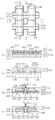
図11(a)〜(e)は、従来例1に係る固体撮像装置の画素構造を示す平面図((a))、水平断面図((d)及び(e))、垂直断面図((b)及び(c))を示しており、該断面図(b)〜(e)の各々は、平面図(a)におけるXIb-XIb線、XIc-XIc線、XId-XId線、XIe-XIe線の断面にそれぞれ対応している。なお、平面図(a)では、便宜上、断面図に示される構成部分の一部の図示を省略している。 11A to 11E are a plan view ((a)), a horizontal sectional view ((d) and (e)), and a vertical sectional view (( b) and (c)), and each of the cross-sectional views (b) to (e) includes an XIb-XIb line, an XIc-XIc line, an XId-XId line, and an XIe-XIe in the plan view (a). Each corresponds to a cross section of the line. In the plan view (a), for the sake of convenience, illustration of some of the components shown in the cross-sectional view is omitted.
図11(a)〜(e)に示すように、従来例1の固体撮像装置の画素構造では、半導体基板41の表面近傍には、垂直方向に延伸する複数の垂直転送チャネル42と、マトリクス状に配置された複数のフォトダイオード(PD)43とが形成されている。半導体基板41上の全面に、複数の垂直転送チャネル42及び複数のフォトダイオード43を覆うように、ゲート絶縁膜44が形成されている。ゲート絶縁膜44の上には、複数の垂直転送チャネル42を覆う一方で複数のフォトダイオード43の各々の一部を露出させるように、ゲート電極45、並びにタングステン、アルミニウム、シリサイド、又はサリサイドなどの金属遮光膜46からなる第1及び第2の垂直転送電極47a及び47bが垂直方向に交互に複数形成されている。さらに、第1の垂直転送電極47aと第2の垂直転送電極47bとの隙間と、複数のフォトダイオード43を露出させる開口部43R((a)参照)に露出する第1及び第2の垂直転送電極47a及び47bの側壁部とに、遮光性樹脂48が形成されている。
As shown in FIGS. 11A to 11E, in the pixel structure of the solid-state imaging device of the first conventional example, a plurality of
また、ゲート絶縁膜44の上には、複数の第1及び第2の垂直転送電極47a及び47bを覆うように、複数のフォトダイオード43の各々の上で凹部を有する層間絶縁膜49が形成されており、該層間絶縁膜49の上には、この層間絶縁膜49の屈折率よりも高い屈折率を持つ高屈折率膜50が形成されている。なお、層間絶縁膜49及び高屈折率膜50によって層内レンズ51が構成される。また、図示しないが、高屈折率膜50の上には、上記図10と同様に、平坦化膜、カラーフィルタ、平坦化膜、及びトップレンズがこの順で形成される。
On the
次に、上記特許文献1に記載された従来例2に係る固体撮像装置の画素構造について説明する。
Next, the pixel structure of the solid-state imaging device according to Conventional Example 2 described in
図12(a)〜(c)は、従来例2に係る固体撮像装置の画素構造を示す平面図((a))、水平断面図((b)及び(c))を示しており、該断面図(b)及び(c)は、平面図(a)におけるXIIb-XIIb線、XIIc-XIIc線の断面にそれぞれ対応している。なお、平面図(a)では、便宜上、断面図に示される構成部分の一部の図示を省略している。また、図11(b)及び(c)で示した垂直断面図は、この従来例2に係る固体撮像装置の場合も同様である。 12A to 12C are a plan view ((a)) and horizontal sectional views ((b) and (c)) showing a pixel structure of a solid-state imaging device according to Conventional Example 2, Cross-sectional views (b) and (c) correspond to the XIIb-XIIb line and XIIc-XIIc line cross sections in the plan view (a), respectively. In the plan view (a), for the sake of convenience, illustration of some of the components shown in the cross-sectional view is omitted. Further, the vertical sectional views shown in FIGS. 11B and 11C are the same in the case of the solid-state imaging device according to Conventional Example 2.
図12(a)〜(c)に示す従来例2に係る固体撮像装置は、上記従来例1に係る固体撮像装置の画素構造と比較すると、遮光性樹脂48の形成されている領域が異なり、その他の構造は同様である。すなわち、従来例2に係る固体撮像装置における遮光性樹脂48は、開口部43Rに露出する第1及び第2の垂直転送電極47a及び47bの側壁部には形成されておらず((a)及び(b)参照)、さらに、第1の垂直転送電極47aと第2の垂直転送電極47bとの間の隙間に形成されている遮光性樹脂48は、開口部43Rに露出する部分が内側に後退して形成されている((a)及び(c)参照)。
しかしながら、上記従来例1に係る固体撮像装置の画素構造では、以下の1)〜3)に説明する問題点が生じる。すなわち、1)図11(a)、(c)及び(d)に示すように、開口部43Rに露出する第1の垂直転送電極47a及び第2の垂直転送電極47bの側壁部には、遮光性樹脂48が形成されているため、開口部43Rの領域が狭く、感度が低下する。また、2)図11(b)〜(e)に示すように、第1の垂直転送電極47a及び第2の垂直転送電極47bの開口部43Rの底部に対する段差が低いため、層内レンズの曲率が小さい。このため、層内レンズ51の集光力が弱く、入射光が広がるため、垂直転送チャネル42に漏れ込み、スミアが悪化する。さらに、3)図11(a)、(b)及び(d)に示すように、第1の垂直転送電極47aと第2の垂直転送電極47bとの間の隙間に埋め込まれる遮光性樹脂48は、金属遮光膜に比べて一般的に遮光性が低いため、太陽光などの強い光を透過してしまい、垂直転送チャネル42に漏れ込み、スミアが悪化する。
However, the pixel structure of the solid-state imaging device according to Conventional Example 1 has problems described in 1) to 3) below. That is, 1) As shown in FIGS. 11A, 11C, and 11D, the side walls of the first
一方、上記従来例2に係る固体撮像装置の画素構造では、図12(a)及び(b)に示すように、遮光性樹脂48は、開口部43Rに露出する第1及び第2の垂直転送電極47a及び47bの側壁部には形成されていないため、開口部43Rの領域は、上記従来例1に係る固体撮像装置の場合に比べて広く、領域12bに示すように、感度が向上する。このように、上記従来例2に係る固体撮像装置によると、上記従来例1に係る固体撮像装置に対する問題点1)は解消できるものの、問題点2)及び3)を解消することはできない。その上、上記従来例2に係る固体撮像装置の画素構造では、図12(c)に示すように、第1の垂直転送電極47aと第2の垂直転送電極47bとの間の隙間に形成されている遮光性樹脂48は、その開口部43Rに露出する部分が内側に後退して形成されるため、第1の垂直転送電極47aと第2の垂直転送電極47bとの間の隙間の端部から入射光が、領域12cにおいて垂直転送チャネル42に入りやすくなり、スミアが悪化するという新たな問題が生じる。
On the other hand, in the pixel structure of the solid-state imaging device according to the conventional example 2, as shown in FIGS. 12A and 12B, the
前記に鑑み、本発明の目的は、感度を高めると共にスミアを低減することにより、撮像画像の画質に優れ、高速動作を可能とする構造を有する固体撮像装置及びその製造方法を提供することである。 In view of the above, an object of the present invention is to provide a solid-state imaging device having a structure that is excellent in image quality of a captured image and enables high-speed operation by increasing sensitivity and reducing smear, and a method for manufacturing the same. .
前記の目的を達成するために、本発明の一形態に係る固体撮像装置は、表面近傍に、各々が垂直方向に延伸する複数の垂直転送チャネル領域と、マトリクス状に互いに間隔を置いて設けられると共に複数の垂直転送チャネル領域の各々と隣り合って設けられた複数の光電変換領域とを有する半導体基板と、半導体基板の上に、各々がゲート電極及び第1の金属遮光膜からなり、複数の光電変換領域の各々を露出させると共に互いに間隔を置いて水平方向に延伸するように、ゲート絶縁膜を介して形成された複数の垂直転送電極と、複数の垂直転送チャネル領域上における複数の垂直転送電極の各々の間に存在する隙間に形成された透明絶縁膜と、複数の垂直転送電極及び透明絶縁膜の上に、少なくとも複数の垂直転送チャネル領域の各々を覆うように第1の層間絶縁膜を介して形成された第2の金属遮光膜とを備えている。 In order to achieve the above object, a solid-state imaging device according to an aspect of the present invention is provided in the vicinity of a surface with a plurality of vertical transfer channel regions each extending in a vertical direction and spaced apart from each other in a matrix. And a semiconductor substrate having a plurality of photoelectric conversion regions provided adjacent to each of the plurality of vertical transfer channel regions, and on the semiconductor substrate, each comprising a gate electrode and a first metal light shielding film, A plurality of vertical transfer electrodes formed through the gate insulating film so as to expose each of the photoelectric conversion regions and extend in the horizontal direction at intervals, and a plurality of vertical transfers on the plurality of vertical transfer channel regions A transparent insulating film formed in a gap existing between each of the electrodes, and a plurality of vertical transfer electrodes and the transparent insulating film covering at least each of the plurality of vertical transfer channel regions; And a second metal light-shielding film formed through the first interlayer insulating film so as.
本発明の一形態に係る固体撮像装置において、透明絶縁膜は、複数の光電変換領域の各々に露出している複数の垂直転送電極の側壁部の各々にさらに形成されている。 In the solid-state imaging device according to an aspect of the present invention, the transparent insulating film is further formed on each of the sidewall portions of the plurality of vertical transfer electrodes exposed to each of the plurality of photoelectric conversion regions.
本発明の一形態に係る固体撮像装置において、第2の金属遮光膜は、垂直方向に並ぶ複数の光電変換領域間における領域の各々の上にさらに形成されている。 In the solid-state imaging device according to an aspect of the present invention, the second metal light-shielding film is further formed on each of the regions between the plurality of photoelectric conversion regions arranged in the vertical direction.
本発明の一形態に係る固体撮像装置において、複数の垂直転送電極は、互いに隣り合う、垂直方向に並ぶ光電変換領域間における領域上を含んで水平方向に延伸する第1の垂直転送電極と、水平方向に並ぶ光電変換領域間における領域上に形成された読み出し電極を兼ねる第2の垂直転送電極とを複数備えてなり、第2の垂直転送電極は、第2の金属遮光膜と電気的に接続されており、第2の金属遮光膜の下部には、第1の垂直転送電極が形成されている。 In the solid-state imaging device according to an aspect of the present invention, the plurality of vertical transfer electrodes includes a first vertical transfer electrode extending in the horizontal direction including the region between the photoelectric conversion regions adjacent to each other and arranged in the vertical direction; A plurality of second vertical transfer electrodes also serving as readout electrodes formed on regions between the photoelectric conversion regions arranged in the horizontal direction, and the second vertical transfer electrodes are electrically connected to the second metal light shielding film. A first vertical transfer electrode is formed below the second metal light shielding film.
本発明の一形態に係る固体撮像装置において、第1の垂直転送電極と第2の垂直転送電極との隙間は、水平方向に並ぶ光電変換領域間の領域における垂直方向の上流側及び下流側に位置している。 In the solid-state imaging device according to an aspect of the present invention, the gap between the first vertical transfer electrode and the second vertical transfer electrode is on the upstream side and the downstream side in the vertical direction in the region between the photoelectric conversion regions arranged in the horizontal direction. positioned.
本発明の一形態に係る固体撮像装置において、第2の金属遮光膜は、垂直方向に分割された複数の部分からなり、第1の垂直転送電極及び第2の垂直転送電極の各々は、第2の金属遮光膜における複数の部分間の隙間が、水平方向に並ぶ光電変換領域間における領域の中央部に位置するように、形成されている。 In the solid-state imaging device according to an aspect of the present invention, the second metal light-shielding film includes a plurality of portions divided in the vertical direction, and each of the first vertical transfer electrode and the second vertical transfer electrode includes The gaps between the plurality of portions of the two metal light shielding films are formed so as to be positioned at the center of the region between the photoelectric conversion regions arranged in the horizontal direction.
本発明の一形態に係る固体撮像装置において、第2の垂直転送電極の各々は、島状に独立して形成されている。 In the solid-state imaging device according to an aspect of the present invention, each of the second vertical transfer electrodes is independently formed in an island shape.
本発明の一形態に係る固体撮像装置において、透明絶縁膜は、シリコン窒化膜よりなる。 In the solid-state imaging device according to an aspect of the present invention, the transparent insulating film is made of a silicon nitride film.
本発明の一形態に係る固体撮像装置において、半導体基板の上に、第2の金属遮光膜を覆うように形成され、複数の光電変換領域の各々の上に凹部を有する第2の層間絶縁膜と、第2の層間絶縁膜の上に形成され、第2の層間絶縁膜の屈折率よりも高い屈折率を有する高屈折率膜とをさらに備えている。 In the solid-state imaging device according to an aspect of the present invention, the second interlayer insulating film is formed on the semiconductor substrate so as to cover the second metal light-shielding film and has a recess on each of the plurality of photoelectric conversion regions. And a high refractive index film formed on the second interlayer insulating film and having a refractive index higher than that of the second interlayer insulating film.
本発明の一形態に係る固体撮像装置において、屈折率膜の上に形成されたカラーフィルタと、カラーフィルタの上に形成されたトップレンズとをさらに備えている。 The solid-state imaging device according to an aspect of the present invention further includes a color filter formed on the refractive index film and a top lens formed on the color filter.
本発明の一形態に係る固体撮像装置の製造方法は、半導体基板の表面近傍に、各々が垂直方向に延伸する複数の垂直転送チャネル領域と、マトリクス状に互いに間隔を置いて設けられると共に複数の垂直転送チャネル領域の各々と隣り合って設けられた複数の光電変換領域とを形成する工程(a)と、半導体基板の上に、各々がゲート電極及び第1の金属遮光膜からなり、複数の光電変換領域の各々を露出させると共に互いに間隔を置いて水平方向に延伸するように、ゲート絶縁膜を介して複数の垂直転送電極を形成する工程(b)と、複数の垂直転送チャネル領域上における複数の垂直転送電極の各々の間に存在する隙間に透明絶縁膜を形成する工程(c)と、複数の垂直転送電極及び透明絶縁膜の上に、少なくとも複数の垂直転送チャネル領域の各々を覆うように第1の層間絶縁膜を介して第2の金属遮光膜を形成する工程(d)とを備える。 A manufacturing method of a solid-state imaging device according to an embodiment of the present invention includes a plurality of vertical transfer channel regions each extending in a vertical direction and provided in the vicinity of a surface of a semiconductor substrate and spaced apart from each other in a matrix. A step (a) of forming a plurality of photoelectric conversion regions provided adjacent to each of the vertical transfer channel regions; and a plurality of gate electrodes and a first metal light-shielding film on the semiconductor substrate, A step (b) of forming a plurality of vertical transfer electrodes through the gate insulating film so as to expose each of the photoelectric conversion regions and extend in the horizontal direction at intervals, and on the plurality of vertical transfer channel regions A step (c) of forming a transparent insulating film in a gap existing between each of the plurality of vertical transfer electrodes; and at least a plurality of vertical transfer channels on the plurality of vertical transfer electrodes and the transparent insulating film. And a (d) forming a second metal light through the first interlayer insulating film so as to cover the respective areas.
本発明の一形態に係る固体撮像装置の製造方法において、前期工程(c)は、半導体基板の全面上に、透明絶縁膜材料を堆積した後に、透明絶縁膜材料に対して異方性エッチングを行うことにより、複数の垂直転送チャネル領域上における複数の垂直転送電極の各々の間に存在する隙間に透明絶縁膜材料を残存させてなる透明絶縁膜を形成する工程を含む。 In the method for manufacturing a solid-state imaging device according to an aspect of the present invention, in the first step (c), after the transparent insulating film material is deposited on the entire surface of the semiconductor substrate, anisotropic etching is performed on the transparent insulating film material. And performing a step of forming a transparent insulating film in which a transparent insulating film material is left in a gap existing between each of the plurality of vertical transfer electrodes on the plurality of vertical transfer channel regions.
本発明の一形態に係る固体撮像装置の製造方法において、工程(c)は、半導体基板の全面上に、透明絶縁膜材料を堆積した後に、透明絶縁膜材料に対して等方性エッチングを行うことにより、複数の垂直転送チャネル領域上における複数の垂直転送電極の各々の間に存在する隙間に透明絶縁膜材料を残存させると共に、複数の光電変換領域の各々に露出している複数の垂直転送電極の側壁部の各々に残存させてなる、透明絶縁膜を形成する工程を含む。 In the method for manufacturing a solid-state imaging device according to an aspect of the present invention, in the step (c), after the transparent insulating film material is deposited on the entire surface of the semiconductor substrate, isotropic etching is performed on the transparent insulating film material. As a result, the transparent insulating film material remains in the gaps between the plurality of vertical transfer electrodes on the plurality of vertical transfer channel regions, and the plurality of vertical transfers exposed in the plurality of photoelectric conversion regions. A step of forming a transparent insulating film left on each of the side wall portions of the electrode.
本発明の一形態に係る固体撮像装置の製造方法において、工程(d)は、垂直方向に並ぶ複数の光電変換領域間における領域の各々の上に第2の金属遮光膜をさらに形成する工程を含む。 In the method for manufacturing a solid-state imaging device according to an aspect of the present invention, the step (d) includes a step of further forming a second metal light-shielding film on each of the regions between the plurality of photoelectric conversion regions arranged in the vertical direction. Including.
本発明の一形態に係る固体撮像装置の製造方法において、工程(b)は、互いに隣り合う、垂直方向に並ぶ光電変換領域間の領域上を含んで水平方向に延伸する第1の垂直転送電極と、水平方向に並ぶ光電変換領域間の領域上に形成された読み出し電極を兼ねる第2の垂直転送電極とを複数備えてなる、複数の垂直転送電極を形成する工程を含み、工程(d)は、第1の層間絶縁膜に設けたコンタクトホールを介して第2の金属遮光膜と電気的に接続されると共に、第1の垂直転送電極を覆うように、第2の金属遮光膜を形成する工程を含む。 In the method for manufacturing a solid-state imaging device according to an aspect of the present invention, the step (b) includes a first vertical transfer electrode extending in the horizontal direction including the region between the photoelectric conversion regions adjacent to each other and arranged in the vertical direction. And a step of forming a plurality of vertical transfer electrodes comprising a plurality of second vertical transfer electrodes that also serve as readout electrodes formed on regions between the photoelectric conversion regions arranged in the horizontal direction, the step (d) Is electrically connected to the second metal light-shielding film through a contact hole provided in the first interlayer insulating film, and a second metal light-shielding film is formed so as to cover the first vertical transfer electrode The process of carrying out is included.
本発明の一形態に係る固体撮像装置の製造方法において、工程(b)は、第1の垂直転送電極と第2の垂直転送電極との隙間が、水平方向に並ぶ光電変換領域間の領域における垂直方向の上流側及び下流側に位置するように行われる。 In the method for manufacturing a solid-state imaging device according to an aspect of the present invention, in the step (b), the gap between the first vertical transfer electrode and the second vertical transfer electrode is in a region between the photoelectric conversion regions arranged in the horizontal direction. It is performed so as to be positioned on the upstream side and the downstream side in the vertical direction.
本発明の一形態に係る固体撮像装置の製造方法において、工程(d)は、垂直方向に分割された複数の部分からなる第2の金属遮光膜を形成する工程を含み、工程(b)は、第1の垂直転送電極及び第2の垂直転送電極の各々が、第2の金属遮光膜における複数の部分間の隙間が、水平方向に並ぶ光電変換領域間における領域の中央部に位置するように、行われる。 In the method for manufacturing a solid-state imaging device according to an aspect of the present invention, the step (d) includes a step of forming a second metal light-shielding film including a plurality of portions divided in the vertical direction, and the step (b) In each of the first vertical transfer electrode and the second vertical transfer electrode, the gap between the plurality of portions in the second metal light-shielding film is positioned at the center of the region between the photoelectric conversion regions arranged in the horizontal direction. To be done.
本発明の一形態に係る固体撮像装置の製造方法において、工程(d)の後に、半導体基板の上に、第2の金属遮光膜を覆うように、複数の光電変換領域の各々の上に凹部を有する第2の層間絶縁膜を形成する工程(e)と、第2の層間絶縁膜の上に、第2の層間絶縁膜の屈折率よりも高い屈折率を有する高屈折率膜を形成する工程(f)とをさらに備える。 In the method for manufacturing a solid-state imaging device according to an aspect of the present invention, after step (d), a recess is formed on each of the plurality of photoelectric conversion regions on the semiconductor substrate so as to cover the second metal light-shielding film. And forming a second refractive index film having a refractive index higher than the refractive index of the second interlayer dielectric film on the second interlayer dielectric film. A step (f).
本発明の一形態に係る固体撮像装置の製造方法において、高屈折率絶縁膜の上にカラーフィルタを形成する工程(g)と、カラーフィルタの上にトップレンズを形成する工程(h)とをさらに備える。 In the method for manufacturing a solid-state imaging device according to an aspect of the present invention, the step (g) of forming a color filter on the high refractive index insulating film and the step (h) of forming a top lens on the color filter are included. Further prepare.
本発明によると、感度を高めると共にスミアを低減し、撮像画像の画質に優れ、高速動作を可能とする固体撮像装置が実現される。 According to the present invention, it is possible to realize a solid-state imaging device that increases sensitivity and reduces smear, has excellent image quality of a captured image, and enables high-speed operation.
以下、本発明の各実施形態について図面を参照しながら説明する。 Hereinafter, embodiments of the present invention will be described with reference to the drawings.
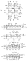
(第1の実施形態)
図1(a)〜(e)は、本発明の第1の実施形態に係る固体撮像装置の画素構造を示す平面図((a))、水平断面図((d)及び(e))、垂直断面図((b)及び(c))を示しており、該断面図(b)〜(e)の各々は、平面図(a)におけるIb-Ib線、Ic-Ic線、Id-Id線、Ie-Ie線の断面にそれぞれ対応している。なお、平面図(a)では、便宜上、断面図に示される構成部分の一部の図示を省略している。また、固体撮像装置の基本的な構成は、上述した図9を用いた説明と同様であって、ここではその説明は省略する。
(First embodiment)
1A to 1E are a plan view (a), a horizontal sectional view (d and e) showing a pixel structure of a solid-state imaging device according to the first embodiment of the present invention, The vertical sectional views ((b) and (c)) are shown, and each of the sectional views (b) to (e) is an Ib-Ib line, an Ic-Ic line, and an Id-Id in the plan view (a). Corresponds to the cross section of the line and the Ie-Ie line. In the plan view (a), for the sake of convenience, illustration of some of the components shown in the cross-sectional view is omitted. Further, the basic configuration of the solid-state imaging device is the same as that described with reference to FIG. 9, and the description thereof is omitted here.
図1(a)〜(e)に示すように、本実施形態に係る固体撮像装置の画素構造では、半導体基板101の表面近傍には、垂直方向に延伸する複数の垂直転送チャネル102と、マトリクス状に配置された複数のフォトダイオード(PD:光電変換領域)103とが形成されている。半導体基板101上の全面に、複数の垂直転送チャネル102及び複数のフォトダイオード103を覆うように、ゲート絶縁膜104が形成されている。ゲート絶縁膜104の上には、複数の垂直転送チャネル102を覆う一方で複数のフォトダイオード103の各々の一部を露出させるように、ゲート電極105、並びにタングステン、アルミニウム、シリサイド、又はサリサイドなどの金属遮光膜106からなる第1及び第2の垂直転送電極107a及び107bが垂直方向に交互に複数形成されている。さらに、第1の垂直転送電極107aと第2の垂直転送電極107bとの隙間と、複数のフォトダイオード103を露出させる開口部103R((a)参照)に露出する第1及び第2の垂直転送電極107a及び107bの側壁部とに、酸化膜(例えばシリコン酸化膜)又は窒化膜(例えばシリコン窒化膜)からなる透明絶縁膜108が形成されている。ここで、透明絶縁膜108の形成方法として異方性エッチングを用いている。
As shown in FIGS. 1A to 1E, in the pixel structure of the solid-state imaging device according to this embodiment, a plurality of
また、ゲート絶縁膜104の上には、複数の第1及び第2の垂直転送電極107a及び107bを覆うように、層間絶縁膜109が形成されており、該層間絶縁膜109の上には、垂直転送チャネル102上を覆うように、金属遮光膜111が形成されている。層間絶縁膜109の上には、金属遮光膜111を覆うように、複数のフォトダイオード103の各々の上で凹部を有する層間絶縁膜112が形成されており、該層間絶縁膜112の上には、この層間絶縁膜112の屈折率よりも高い屈折率を持つ高屈折率膜113が形成されている。なお、層間絶縁膜112及び高屈折率膜113によって層内レンズ114が構成される。また、図示しないが、高屈折率膜113の上には、平坦化膜、カラーフィルタ、平坦化膜、及びトップレンズがこの順で形成される(例えば上述した図10参照)。
Further, an
以上の画素構造を有する本実施形態に係る固体撮像装置によると、図1(a)、(c)〜(e)に示すように、複数のフォトダイオード103を露出させる開口部103Rに露出する第1及び第2の垂直転送電極107a及び107bの側壁部には、上記従来例1の遮光性樹脂とは異なり、酸化膜(例えばシリコン酸化膜)又は窒化膜(例えばシリコン窒化膜)からなる透明絶縁膜108が形成されているため、フォトダイオード103の開口部103Rの大きさは、実質的に第1及び第2の垂直転送電極107a及び107bと金属遮性遮光膜111とで決まり、上記従来例1と比べて実質的に広くなるので、感度が上記従来例1に比べて向上する。
According to the solid-state imaging device according to the present embodiment having the above-described pixel structure, as shown in FIGS. 1A and 1C, the first exposed
また、図1(d)及び(e)に示すように、第1及び第2の垂直転送電極107a及び107b上には、金属遮光膜111が形成されているため、金属遮光膜111の上面からフォトダイオード103までの段差は上記従来例1の場合に比べて大きくなる。このため、層内レンズ114を構成する層間絶縁膜112には、フォトダイオード103上に、従来例1の場合に比べて深さが深い凹部が形成される。このため、層間絶縁膜112及び高屈折率膜113からなる層内レンズ114の曲率が大きくなる。その結果、例えば図1(d)の領域1dRに示すように、層内レンズ114の集光力が強まり、入射光Lの広がりが抑制され、従来例1の場合に比べてスミアが改善される。
Further, as shown in FIGS. 1D and 1E, since the metal light-shielding
また、図1(a)、(c)〜(e)に示すように、第1の垂直転送電極107aと第2の垂直転送電極107bとの間の隙間上には、上記従来例1の場合の遮光性樹脂よりも遮光性の高い金属遮光膜111が形成されているため、太陽光などの強い光が入射しても透過が抑制される。このように、例えば図1(e)の領域1eRに透過する光が上記従来例1の場合に比べて抑制されるため、本実施形態では上記従来例1の場合に比べてスミアが改善される。
Further, as shown in FIGS. 1A, 1C, and 1E, in the case of the above-described conventional example 1, the gap between the first
さらに、透明絶縁膜108を構成する材料として、例えばシリコン窒化膜などの誘電率の高い窒化膜を用いた場合には、図1(b)に示す断面において、第1の垂直転送電極107aと第2の垂直転送電極107bとの間の電気的な隙間が狭まるため、第1の垂直転送電極107aと第2の垂直転送電極107bとの間の隙間に起因する転送効率の劣化を抑制することができる。
Further, when a nitride film having a high dielectric constant, such as a silicon nitride film, is used as a material constituting the transparent
−第1の実施形態の変形例1−
次に、本実施形態の変形例1に係る固体撮像装置の画素構造について説明する。
-
Next, a pixel structure of the solid-state imaging device according to the first modification of the present embodiment will be described.
図2(a)〜(c)は、本実施形態の変形例1に係る固体撮像装置の画素構造を示す平面図((a))、水平断面図((b)及び(c))を示しており、該断面図(b)及び(c)は、平面図(a)におけるIIb-IIb線、IIc-IIc線の断面にそれぞれ対応している。なお、平面図(a)では、便宜上、断面図に示される構成部分の一部の図示を省略している。また、図1(b)で示した垂直断面図は、本変形例1に係る固体撮像装置の場合も同様であり、図1(c)に示した垂直断面図における第1及び第2の垂直転送電極107a及び107bの側壁に位置する透明絶縁膜が存在しない構造が、本変形例1に係る固体撮像装置の対応する断面構造に相当する。
2A to 2C are a plan view (a) and a horizontal sectional view (b and c) showing a pixel structure of a solid-state imaging device according to the first modification of the present embodiment. The cross-sectional views (b) and (c) correspond to the cross sections taken along the lines IIb-IIb and IIc-IIc in the plan view (a), respectively. In the plan view (a), for the sake of convenience, illustration of some of the components shown in the cross-sectional view is omitted. The vertical sectional view shown in FIG. 1B is the same as that of the solid-state imaging device according to the first modification, and the first and second vertical sections in the vertical sectional view shown in FIG. The structure in which the transparent insulating film located on the side walls of the
図2(a)〜(c)に示す本変形例1に係る固体撮像装置は、図1(a)〜(e)に示した固体撮像装置の画素構造と比較すると、透明絶縁膜108の形成されている領域が異なり、その他の構造は同様である。すなわち、本変形例1に係る固体撮像装置における透明絶縁膜108は、図2(a)〜(c)に示すように、開口部103Rに露出する第1及び第2の垂直転送電極107a及び107bの側壁部には形成されておらず、さらに、第1の垂直転送電極107aと第2の垂直転送電極107bとの間の隙間に形成されている透明絶縁膜108は、開口部103Rに露出する部分が内側に後退して形成されている(図2(c)参照)。ここで、透明絶縁膜108の形成方法として等方性エッチングを用いている。
The solid-state imaging device according to the first modification shown in FIGS. 2A to 2C has a transparent
以上の画素構造を有する本変形例1に係る固体撮像装置によると、図2(a)及び(c)に示すように、第1の垂直転送電極107aと第2の垂直転送電極107bとの間の隙間に形成されている透明絶縁膜108は、開口部103Rに露出する部分が内側に後退して形成されているが、第1の垂直転送電極107aと第2の垂直転送電極107bとの間の隙間上は金属遮光膜111で遮光されるため、入射光が、第1の垂直転送電極47aと第2の垂直転送電極47bとの間の隙間の端部から、例えば領域2cRにおいて垂直転送チャネル42に入りやすいということが抑制され、上記従来例2の場合に比べてスミアが改善される。
According to the solid-state imaging device according to the first modification example having the above-described pixel structure, as shown in FIGS. 2A and 2C, the first
また、図2(b)に示すように、透明絶縁膜108は、等方性エッチングにより、開口部103Rに露出する第1及び第2の垂直転送電極107a及び107bの側壁部には形成されないため、転送効率を向上させるために透明絶縁膜108として窒化膜(例えばシリコン窒化膜)などの誘電率の高い材料を用いた場合であっても、透明絶縁膜108のエッジに入射した光が屈折して半導体基板101内で広がる(図1(d)及び(e)参照)ことなく、例えば領域2bRに示すように垂直に入射する。このため、図1(a)〜(e)に示した固体撮像装置において誘電率の高い材料からなる透明絶縁膜108を用いた場合に比べてスミアが更に改善される。
Further, as shown in FIG. 2B, the transparent
−第1の実施形態の変形例2−
次に、本実施形態の変形例2に係る固体撮像装置の画素構造について説明する。
-
Next, a pixel structure of a solid-state imaging device according to
図3(a)、(c)〜(e)は、本実施形態の変形例2に係る固体撮像装置の画素構造を示す平面図((a))、垂直断面図((c))、水平断面図((d)及び(e))を示しており、該断面図(c)〜(e)は、平面図(a)におけるIIIc-IIIc線、IIId-IIId線、IIIe-IIIe線の断面にそれぞれ対応している。なお、平面図(a)では、便宜上、断面図に示される構成部分の一部の図示を省略している。また、図1(b)で示した垂直断面図は、本変形例2に係る固体撮像装置における対応する断面も同様である。また、図3(d)及び(e)に示す水平断面図は、上記図1(d)及び(e)に示した垂直断面図と同じである。さらに、図3(b)に示した垂直断面図は、本変形例2に対する比較例として上記図1(c)の垂直断面図に入射光Lをさらに示した図である。 3A, 3C to 3E are a plan view (a), a vertical sectional view (c), and a horizontal view showing a pixel structure of a solid-state imaging device according to the second modification of the present embodiment. Sectional views ((d) and (e)) are shown, and the sectional views (c) to (e) are cross sections taken along lines IIIc-IIIc, IIId-IIId, and IIIe-IIIe in the plan view (a). It corresponds to each. In the plan view (a), for the sake of convenience, illustration of some of the components shown in the cross-sectional view is omitted. Further, the vertical sectional view shown in FIG. 1B is the same in the corresponding cross section in the solid-state imaging device according to the second modification. 3D and 3E are the same as the vertical sectional views shown in FIGS. 1D and 1E. Further, the vertical cross-sectional view shown in FIG. 3B is a view further showing the incident light L in the vertical cross-sectional view of FIG.
図3(a)、(c)〜(e)に示す本変形例2に係る固体撮像装置は、図1(a)〜(e)に示した固体撮像装置の画素構造と比較すると、金属遮光膜111の形成されている領域が異なり、その他の構造は同様である。すなわち、本変形例2に係る固体撮像装置における金属遮光膜111は、垂直転送チャネル102の上に形成されているのみならず、垂直画素分離部上、すなわち、垂直方向に並ぶ隣り合うフォトダイオード103間の領域上にも形成されている。
Compared with the pixel structure of the solid-state imaging device shown in FIGS. 1A to 1E, the solid-state imaging device according to the second modification shown in FIGS. The region where the
以上の画素構造を有する本変形例2に係る固体撮像装置によると、図3(a)及び(c)に示すように、金属遮光膜111は、垂直画素分離部上にも形成されているため、垂直分離部上における第1の垂直転送電極107aと第2の垂直転送電極107bとの間の隙間は遮光される。このため、上記図1(c)に示す構造のように垂直画素分離部上に金属遮光膜111が形成されていないと、図3(b)に示すように、入射光の周辺の斜め光が、垂直分離部上における第1の垂直転送電極107aと第2の垂直転送電極107bとの間の隙間や、垂直画素分離部上の第1及び第2の垂直転送電極107a及び107b上を通過して隣り合うフォトダイード103に入り込んでクロストークの原因となるが、本変形例2によるとこのクロストークが抑制される。
According to the solid-state imaging device according to the second modification having the above pixel structure, as shown in FIGS. 3A and 3C, the metal light-shielding
また、図3(c)に示すように、金属遮光膜111は、垂直転送チャネル102の上に形成されているのみならず、垂直画素分離部上にも形成されているため、開口部103Rにおける垂直画素分離部に隣接する部分のフォトダイオード103に対する段差が大きくなる。このため、層内レンズ114の曲率もより大きくなる結果、層内レンズ114の集光力が強まり、入射光Lの蹴られが抑制されるため、上記図1(a)〜(e)に示した固体撮像装置の場合よりも感度及び光の入射角特性が向上する。
Further, as shown in FIG. 3C, the metal light-shielding
なお、本変形例2では、上記図1(a)〜(e)に示した固体撮像装置の構造に対して金属遮光膜111の形状が変更された構造である場合について説明したが、同様に、上記図2(a)〜(c)に示した変形例1に対しても適用できる構造であって、クロストーク低減及び感度向上という効果を得ることができる。
In the second modification, the case where the shape of the metal light-shielding
(第2の実施形態)
図4(a)〜(e)は、本発明の第2の実施形態に係る固体撮像装置の画素構造を示す平面図((a))、水平断面図((d)及び(e))、垂直断面図((b)及び(c))を示しており、該断面図(b)〜(e)の各々は、平面図(a)におけるIVb-IVb線、IVc-IVc線、IVd-IVd線、IVe-IVe線の断面にそれぞれ対応している。なお、平面図(a)では、便宜上、断面図に示される構成部分の一部の図示を省略している。また、固体撮像装置の基本的な構成は、上述した図9を用いた説明と同様であって、ここではその説明は省略する。
(Second Embodiment)
4A to 4E are a plan view ((a)), a horizontal sectional view ((d) and (e)) showing a pixel structure of a solid-state imaging device according to the second embodiment of the present invention, The vertical sectional views ((b) and (c)) are shown, and each of the sectional views (b) to (e) is IVb-IVb line, IVc-IVc line, IVd-IVd in the plan view (a). Corresponds to the cross section of the line IVe-IVe. In the plan view (a), for the sake of convenience, illustration of some of the components shown in the cross-sectional view is omitted. Further, the basic configuration of the solid-state imaging device is the same as that described with reference to FIG. 9, and the description thereof is omitted here.
図4(a)〜(e)に示すように、本実施形態に係る固体撮像装置の画素構造では、半導体基板101の表面近傍には、垂直方向に延伸する複数の垂直転送チャネル102と、マトリクス状に配置された複数のフォトダイオード(PD)103とが形成されている。半導体基板101上の全面に、複数の垂直転送チャネル102及び複数のフォトダイオード103を覆うように、ゲート絶縁膜104が形成されている。ゲート絶縁膜104の上には、複数の垂直転送チャネル102を覆う一方で複数のフォトダイオード103の各々の一部を露出させるように、ゲート電極105、並びにタングステン、アルミニウム、シリサイド、又はサリサイドなどの金属遮光膜106からなる第1及び第2の垂直転送電極107a及び107bが垂直方向に交互に複数形成されている。ここで、第1の垂直転送電極107aは、垂直方向に並ぶフォトダイオード103間の領域に存在する垂直画素分離部上を水平方向に延伸するように形成されている。また、第2の垂直転送電極107bは、水平方向に並ぶフォトダイオード103間の領域に島状に独立して形成されている。
As shown in FIGS. 4A to 4E, in the pixel structure of the solid-state imaging device according to this embodiment, a plurality of
さらに、第1の垂直転送電極107aと第2の垂直転送電極107bとの隙間には、酸化膜(例えばシリコン酸化膜)又は窒化膜(例えばシリコン窒化膜)からなる透明絶縁膜108が形成されている。ここで、透明絶縁膜108の形成方法として異方性エッチングを用いることで、第1の垂直転送電極107aと第2の垂直転送電極107bとの隙間に形成された透明絶縁膜108は、開口部143に露出する部分が内側に後退して形成されている。
Further, a transparent
また、ゲート絶縁膜104の上には、複数の第1及び第2の垂直転送電極107a及び107bを覆うように、層間絶縁膜109が形成されており、該層間絶縁膜109にはコンタクトホールが形成されており、該コンタクトホールには金属膜が埋め込まれてなるコンタクト140が形成されている。層間絶縁膜109の上には、垂直転送チャネル102上を覆うように、コンタクト140を介して第2の垂直転送電極107bと接続する金属遮光膜111が形成されている。層間絶縁膜109の上には、金属遮光膜111を覆うように、複数のフォトダイオード103の各々の上で凹部を有する層間絶縁膜112が形成されており、該層間絶縁膜112の上には、この層間絶縁膜112の屈折率よりも高い屈折率を持つ高屈折率膜113が形成されている。なお、層間絶縁膜112及び高屈折率膜113によって層内レンズ114が構成される。また、図示しないが、高屈折率膜113の上には、平坦化膜、カラーフィルタ、平坦化膜、及びトップレンズがこの順で形成される(例えば上述した図10参照)。
Further, an
以上のように、図4(a)〜(e)に示した本実施形態に係る固体撮像装置の画素構造では、金属遮光膜111が、コンタクト140を介して第2の垂直転送電極107bと接続されており、金属遮光膜111を介して転送パルスが供給される構造となっている。また、第2の垂直転送電極107bが、島状の独立した形状を有し、フォトダイオード103に隣り合うように形成されているため、第1の垂直転送電極107aと第2の垂直転送電極107bとの間の隙間が、水平方向に並ぶフォトダイード103間の領域であって、その上流側及び下流側に位置している。
As described above, in the pixel structure of the solid-state imaging device according to this embodiment shown in FIGS. 4A to 4E, the metal
以上の画素構造を有する本実施形態に係る固体撮像装置によると、図4(a)に示すように、第2の垂直転送電極107bが、フォトダイオード103の中央部に隣り合うように形成されているため、第1の垂直転送電極107aと第2の垂直転送電極107bとの間の隙間が、水平方向に並ぶフォトダイード103間の領域における上流端及び下流端付近に形成される。このため、例えば図4(e)に示すように、この隙間には、層内レンズ114で集められた光の周辺の光Leであるためにほとんど入射することがない。その結果、本実施形態では、上記第1の実施形態の場合に比べて、この隙間部分における領域4eRへの光の漏れ込みによるスミアが大幅に改善される。
According to the solid-state imaging device according to the present embodiment having the above pixel structure, the second
また、図4(a)及び(c)に示すように、第2の垂直転送電極107bに転送パルスを供給する金属遮光膜111は、第1の垂直転送電極107a上に重なるように形成されるため、垂直方向に並ぶフォトダイード103間の領域である垂直画素分離部の配線幅を狭めることができる。その結果、開口部143の垂直方向における開口幅を大幅に広げることができるため、感度が更に向上する。
Further, as shown in FIGS. 4A and 4C, the metal
さらに、第2の垂直転送電極107bに高電圧(12V)の読み出しパルスを印加しても、図4(a)及び(c)に示すように、垂直画素分離部上では、金属遮光膜111の下部には第1の垂直転送電極107aが形成されているため、第1の垂直転送電極107aがシールド電極として働くので、垂直画素分離部の基板部分に対して読み出しパルスの電界が加わらず、フォトダイオード103から信号電荷を安定して読み出すことが可能となる。
Further, even when a high voltage (12V) readout pulse is applied to the second
−第2の実施形態の変形例−
次に、本実施形態の変形例に係る固体撮像装置の画素構造について説明する。
-Modification of the second embodiment-
Next, a pixel structure of a solid-state imaging device according to a modification example of the present embodiment will be described.
図5(a)〜(c)は、本実施形態の変形例に係る固体撮像装置の画素構造を示す平面図((a))、垂直断面図((b))、水平断面図((c))を示しており、該断面図(b)及び(c)は、平面図(a)におけるVb-Vb線、Vc-Vc線の断面にそれぞれ対応している。なお、平面図(a)では、便宜上、断面図に示される構成部分の一部の図示を省略している。また、図4(c)で示した垂直断面図は、本変形例に係る固体撮像装置の対応する断面構造に相当する。 5A to 5C are a plan view (a), a vertical cross-sectional view (b), and a horizontal cross-sectional view ((c) showing a pixel structure of a solid-state imaging device according to a modification of the present embodiment. )), And the cross-sectional views (b) and (c) correspond to the cross-sections of the Vb-Vb line and the Vc-Vc line in the plan view (a), respectively. In the plan view (a), for the sake of convenience, illustration of some of the components shown in the cross-sectional view is omitted. Further, the vertical sectional view shown in FIG. 4C corresponds to a corresponding sectional structure of the solid-state imaging device according to this modification.
図5(a)〜(c)に示す本変形例に係る固体撮像装置は、図4(a)〜(e)に示した固体撮像装置の画素構造と比較すると、第1及び第2の垂直転送電極107a及び107bの形成位置が異なり、その他の構造は同様である。すなわち、第1の垂直転送電極107aにおける垂直転送チャネル102上の部分と垂直画素分離部上の部分とが垂直方向に互いに異なる方向にその上下位置をずらして配置することにより、第2の垂直転送電極107bの上下位置も垂直方向にずらして配置することができる。このため、本実施形態では、コンタクト140を介して第2の垂直転送電極107bに接続する金属遮光膜111の垂直転送チャネル102上の隙間の位置が、水平方向に並ぶフォトダイオード103間の領域であって且つフォトダイード103の中央部付近になるように構成されている。
Compared with the pixel structure of the solid-state imaging device shown in FIGS. 4A to 4E, the solid-state imaging device according to this modification shown in FIGS. The formation positions of the
以上の画素構造を有する本実施形態に係る固体撮像装置によると、金属遮光膜111の垂直転送チャネル102上の隙間の位置が、水平方向に並ぶフォトダイオード103間の領域であって且つフォトダイード103の中央部付近に位置しているため、層内レンズ114の集光スポットSは、画素の中心に形成されるようになるため、入射光のけられが抑制され、感度がより一層向上する。すなわち、上記図4(a)〜(e)に示した固体撮像装置の画素構造では、図4(c)に示すように、集光スポットSの中心Saは、画素の中心Cよりも距離w分ずれた構造であるが、本変形例に係る固体撮像装置の画素構造では、図5(c)に示すように、集光スポットSの中心Saと画素の中心Cとが一致するため、上記のように、感度がより一層向上する。
According to the solid-state imaging device according to this embodiment having the above pixel structure, the position of the gap on the
(第3の実施形態)
以下、本発明の第3の実施形態に係る固体撮像装置の製造方法について説明する。
(Third embodiment)
Hereinafter, a method for manufacturing the solid-state imaging device according to the third embodiment of the present invention will be described.
図6(a)〜(d)及び図7(a)〜(d)は、本発明の第3の実施形態に係る固体撮像装置の製造方法を工程順に示す断面図であって、本実施形態では、上記第1及び第2の実施形態に係る固体撮像装置のうち、図4(a)〜(e)に示した画素構造を有する固体撮像装置の製造方法を例にして説明する。また、図6及び図7の(a)〜(d)の各図では、紙面に向かって左側に図4(b)に対応する垂直断面を示しており、紙面に向かって右側に図4(d)に対応する水平断面図を示している。なお、上記第1及び第2の実施形態に係る固体撮像装置のうちの他の画素構造を有する固体撮像装置の一連の製造方法については特に説明しないが、以下に説明する製造方法から容易に想定できるものである。 FIGS. 6A to 6D and FIGS. 7A to 7D are cross-sectional views illustrating a method of manufacturing a solid-state imaging device according to the third embodiment of the present invention in the order of steps, and this embodiment. In the solid-state imaging device according to the first and second embodiments, a manufacturing method of the solid-state imaging device having the pixel structure shown in FIGS. 4A to 4E will be described as an example. Also, in each of FIGS. 6 and 7A to 7D, the vertical cross section corresponding to FIG. 4B is shown on the left side toward the paper surface, and FIG. A horizontal sectional view corresponding to d) is shown. Note that a series of manufacturing methods for a solid-state imaging device having another pixel structure among the solid-state imaging devices according to the first and second embodiments will not be described in particular, but can be easily assumed from the manufacturing methods described below. It can be done.
まず、図6(a)に示すように、半導体基板101の表面部分に、垂直方向に延伸する複数の垂直転送チャネル102、及びマトリクス状に配置された複数のフォトダイオード(PD)103を形成した後、半導体基板101上の全面に、複数の垂直転送チャネル102及び複数のフォトダイオード103を覆うように、ゲート絶縁膜104を形成する。続いて、ゲート絶縁膜104の上に、ゲート電極膜105、並びにタングステン、アルミニウム、シリサイド、又はサリサイドなどの金属遮光膜106を形成する。
First, as shown in FIG. 6A, a plurality of
次に、図6(b)に示すように、金属遮光膜106の上に、所望の形状を有するようにレジストパターン150を形成した後に、該レジストパターン150を用いたエッチングにより、複数の垂直転送チャネル102を覆う一方で複数のフォトダイオード103の各々の一部を露出させるように、パターン化されたゲート電極膜105であるゲート電極105及び金属遮光膜106からなる第1及び第2の垂直転送電極107a及び107bを垂直方向に交互に複数形成する。ここでは、1つのレジストパターン150を用いて、ゲート電極膜105及び金属遮光膜106を単一の工程でエッチングする場合について説明したが、ゲート電極膜105及び金属遮光膜106の各々のエッチング工程をそれぞれ別の工程として行ってもよい。また、以上の(a)及び(b)に示した工程の変形例については後述する。
Next, as shown in FIG. 6B, after a resist
次に、図6(c)に示すように、半導体基板101の全面上に、第1及び第2の垂直転送電極107a及び107bを覆うように、酸化膜(例えばシリコン酸化膜)又は窒化膜(シリコン窒化膜)からなる透明絶縁膜材料108を形成する。
Next, as shown in FIG. 6C, an oxide film (for example, a silicon oxide film) or a nitride film (for example, a silicon oxide film) is formed on the entire surface of the
次に、図6(d)に示すように、透明絶縁膜材料108を等方性エッチングすることにより、第1の垂直転送電極107aと第2の垂直転送電極107bとの隙間に、透明絶縁膜材料108が残存してなる透明絶縁膜108を形成する。なお、ここでは、等方性エッチングを用いる場合について説明したが、透明絶縁膜材料108を異方性エッチングすることにより、第1の実施形態の変形例1及び変形例3のように、第1の垂直転送電極107aと第2の垂直転送電極107bとの隙間のみならず、複数のフォトダイオード103を露出させる開口部103R(例えば図1参照)に露出する第1及び第2の垂直転送電極107a及び107bの側壁部に、透明絶縁膜材料108を残存させてなる透明絶縁膜108を形成してもよい。
Next, as shown in FIG. 6D, the transparent insulating
次に、図7(a)に示すように、半導体基板101の全面上に、第1及び第2の垂直転送電極107a及び107b、並びに透明絶縁膜108を覆うように、層間絶縁膜109を形成する。続いて、層間絶縁膜109上に、所望のパターンを有するレジストパターン151を形成した後、該レジストパターン151を用いたエッチングにより、第2の垂直転送電極107bを露出するコンタクトホール152を形成する。なお、ここでは、コンタクトホール152を形成する工程について説明したが、上記第1の実施形態の各固体撮像装置を製造する場合にはその工程は不要である。
Next, as shown in FIG. 7A, an
次に、図7(b)に示すように、コンタクトホール152の内部を含む層間絶縁膜109上に、金属膜を形成した後、該金属膜の上に所望のパターンを有するレジストパターン153を形成する。続いて、レジストパターン153を用いて、金属膜をエッチングすることにより、金属膜がコンタクトホールに埋め込まれてなるコンタクト140を介して第2の垂直転送電極107bと接続する金属遮光膜111を形成する。
Next, as shown in FIG. 7B, after forming a metal film on the
次に、図7(c)に示すように、金属遮光膜111を覆うように、例えばBPSG膜などからなる層間絶縁膜112を形成した後、熱フローや等方性エッチングにより、層間絶縁膜112における各フォトダイオード103の上の部分を凹ませる。続いて、層間絶縁膜112の上に、層間絶縁膜112よりも屈折率の高い高屈折率膜113を形成し、該高屈折率膜113の上にフォトレジスト154を形成する。
Next, as shown in FIG. 7C, an
次に、図7(d)に示すように、フォトレジスト154及び高屈折率膜113をエッチバックすることにより、高屈折率膜113及び層間絶縁膜112からなる層内レンズ114を形成する。
Next, as shown in FIG. 7D, the
なお、以降の工程としては、図示していないが、公知の方法により、平坦化膜、カラーフィルタ、平坦化膜、及びトップレンズをこの順に形成する(例えば上述した図10参照)。 Although not shown in the drawings, the planarizing film, the color filter, the planarizing film, and the top lens are formed in this order by a known method (for example, see FIG. 10 described above).
また、以上の第5の実施形態において、上記図6(a)及び(b)に示した工程の代わりとして、以下で説明する図8(a)〜(c)に示す工程を採用することもできる。 Moreover, in the above 5th Embodiment, the process shown to FIG. 8 (a)-(c) demonstrated below is employ | adopted instead of the process shown to the said FIG.6 (a) and (b). it can.
すなわち、図8(a)に示すように、半導体基板101の表面部分に、図6(a)と同様に複数の垂直転送チャネル102及び複数のフォトダイオード103を形成した後、半導体基板101上の全面にゲート絶縁膜104を形成する。続いて、ゲート絶縁膜の上にゲート電極膜105を形成した後、図示しないレジストパターンを用いたエッチングにより、該ゲート電極膜105を所望の形状にパターニングする。続いて、半導体基板101の全面上に、ゲート電極膜105がパターニングされてなるゲート電極105を覆うように、絶縁膜160を形成する。
That is, as shown in FIG. 8A, a plurality of
次に、図8(b)に示すように、図示しないレジストパターンを用いたエッチングにより、ゲート電極105を露出する開口部を絶縁膜160に形成した後、該開口部を含む絶縁膜160の上に、タングステン、アルミニウム、シリサイド、又はサリサイドなどの金属遮光膜材料106を形成する。
Next, as shown in FIG. 8B, an opening exposing the
次に、図8(c)に示すように、例えば図6(b)のレジストパターン150を用いたエッチングにより、金属遮光膜材料106がパターニングされてなる金属遮光膜106を形成する。なお、その後の工程は、上記図6(c)及び(d)並びに図7(a)〜(d)と同様である。
Next, as shown in FIG. 8C, the metal
以上のように、図8(a)〜(c)に示した工程を採用すると、上記図6(a)及び(b)に示した工程におけるゲート電極膜105及び金属遮光性膜材料106のエッチングによって生じ得る金属が半導体基板を汚染し、暗電流や画素欠陥などの画質不良を引き起こすことを抑制することができる。
As described above, when the steps shown in FIGS. 8A to 8C are adopted, the etching of the
本発明は、固体撮像装置、特にはCCD型の固体撮像装置、及びその製造方法にとって有用である。 The present invention is useful for a solid-state imaging device, in particular, a CCD type solid-state imaging device and a manufacturing method thereof.
101 半導体基板
102 垂直転送チャネル
103 フォトダイオード
103R 開口部
104 ゲート絶縁膜
105 ゲート電極(ゲート電極膜)
106 金属遮光膜
107a 第1の垂直転送電極
107b 第2の垂直転送電極
108 透明絶縁膜
109 層間絶縁膜
111 金属遮光膜(金属遮光膜材料)
112 層間絶縁膜
113 高屈折率膜
114 層内レンズ
115
L 入射光
Le 入射光の周辺の光
1eR、2bR、2cR、4eR、
S スポット
Sa スポットの中心
C フォトダイオードの中心
w 距離
140 コンタクト
143 開口部
150、151、153 レジストパターン
152 コンタクトホール
160 絶縁膜
101
106 Metal
112
L Incident light Le Light around the incident light 1eR, 2bR, 2cR, 4eR,
S Spot Sa Spot center C Photodiode
Claims (17)
前記半導体基板の上に、各々がゲート電極及び第1の金属遮光膜からなり、前記複数の光電変換領域の各々を露出させると共に互いに間隔を置いて水平方向に延伸するように、ゲート絶縁膜を介して形成された複数の垂直転送電極と、
前記複数の垂直転送チャネル領域上における前記複数の垂直転送電極の各々の間に存在する隙間に形成された透明絶縁膜と、
前記複数の垂直転送電極及び前記透明絶縁膜の上に、少なくとも前記複数の垂直転送チャネル領域の各々を覆うように第1の層間絶縁膜を介して形成された第2の金属遮光膜とを備えており、
前記複数の垂直転送電極は、互いに隣り合う、垂直方向に並ぶ前記光電変換領域間における領域上を含んで水平方向に延伸する第1の垂直転送電極と、水平方向に並ぶ前記光電変換領域間における領域上に島状に形成された読み出し電極を兼ねる第2の垂直転送電極とを複数備えてなり、
前記第2の垂直転送電極のみが、前記第2の金属遮光膜と電気的に接続されており、
前記第2の金属遮光膜の下部には、前記第1の垂直転送電極が形成されており、前記
第2の金属遮光膜は、前期垂直転送チャネル領域上の前記第1の金属遮光膜の隙間を完全
に覆うように形成されている、固体撮像装置。 In the vicinity of the surface, a plurality of vertical transfer channel regions each extending in the vertical direction, and a plurality of photoelectric conversions provided adjacent to each of the plurality of vertical transfer channel regions in a matrix and spaced from each other A semiconductor substrate having a region;
A gate insulating film is formed on the semiconductor substrate, each of which includes a gate electrode and a first metal light-shielding film, and exposes each of the plurality of photoelectric conversion regions and extends in the horizontal direction at intervals. A plurality of vertical transfer electrodes formed therebetween,
A transparent insulating film formed in a gap existing between each of the plurality of vertical transfer electrodes on the plurality of vertical transfer channel regions;
And a second metal light-shielding film formed on the plurality of vertical transfer electrodes and the transparent insulating film via a first interlayer insulating film so as to cover at least each of the plurality of vertical transfer channel regions. And
The plurality of vertical transfer electrodes include a first vertical transfer electrode extending in a horizontal direction including a region between the photoelectric conversion regions adjacent to each other and arranged in the vertical direction, and between the photoelectric conversion regions arranged in the horizontal direction. A plurality of second vertical transfer electrodes that also serve as readout electrodes formed in an island shape on the region;
Only the second vertical transfer electrode is electrically connected to the second metal light shielding film,
The first vertical transfer electrode is formed under the second metal light shielding film ,
The second metal light shielding film completely fills the gap between the first metal light shielding films on the vertical transfer channel region in the previous period.
A solid-state imaging device formed so as to cover the surface.
前記透明絶縁膜は、前記複数の光電変換領域の各々に露出している前記複数の垂直転送電極の側壁部の各々にさらに形成されている、固体撮像装置。 The solid-state imaging device according to claim 1,
The solid-state imaging device, wherein the transparent insulating film is further formed on each of side walls of the plurality of vertical transfer electrodes exposed to each of the plurality of photoelectric conversion regions.
前記第2の金属遮光膜は、垂直方向に並ぶ前記複数の光電変換領域間における領域の各々の上にさらに形成されている、固体撮像装置。 The solid-state imaging device according to claim 1 or 2,
The solid-state imaging device, wherein the second metal light shielding film is further formed on each of the regions between the plurality of photoelectric conversion regions arranged in the vertical direction.
前記第1の垂直転送電極と前記第2の垂直転送電極との隙間は、水平方向に並ぶ前記光
電変換領域間の領域における垂直方向の上流側及び下流側に位置している、固体撮像装置。 The solid-state imaging device according to claim 1,
The solid-state imaging device, wherein the gap between the first vertical transfer electrode and the second vertical transfer electrode is located on the upstream side and the downstream side in the vertical direction in the region between the photoelectric conversion regions arranged in the horizontal direction.
前記第2の金属遮光膜は、垂直方向に分割された複数の部分からなり、
前記第2の金属遮光膜における前記複数の部分間の隙間が、水平方向に並ぶ前記光電変換領域間における領域の中央部に位置するように、形成されている、固体撮像装置。 The solid-state imaging device according to claim 1,
The second metal light-shielding film is composed of a plurality of parts divided in the vertical direction ,
A solid-state imaging device, wherein a gap between the plurality of portions in the second metal light-shielding film is formed so as to be positioned at a central portion of a region between the photoelectric conversion regions arranged in a horizontal direction.
前記第2の垂直転送電極の各々は、島状に独立して形成されている、固体撮像装置。 The solid-state imaging device according to claim 5 ,
Each of the second vertical transfer electrodes is a solid-state imaging device that is independently formed in an island shape.
前記透明絶縁膜は、シリコン窒化膜よりなる、固体撮像装置。 The solid-state imaging device according to any one of claims 1 to 6,
The solid-state imaging device, wherein the transparent insulating film is made of a silicon nitride film.
前記半導体基板の上に、前記第2の金属遮光膜を覆うように形成され、前記複数の光電変換領域の各々の上に凹部を有する第2の層間絶縁膜と、
前記第2の層間絶縁膜の上に形成され、前記第2の層間絶縁膜の屈折率よりも高い屈折率を有する高屈折率膜とをさらに備えている、固体撮像装置。 The solid-state imaging device according to any one of claims 1 to 7,
A second interlayer insulating film formed on the semiconductor substrate so as to cover the second metal light-shielding film and having a recess on each of the plurality of photoelectric conversion regions;
A solid-state imaging device, further comprising: a high refractive index film formed on the second interlayer insulating film and having a refractive index higher than that of the second interlayer insulating film.
前記高屈折率膜の上に形成されたカラーフィルタと、
前記カラーフィルタの上に形成されたトップレンズとをさらに備えている、固体撮像装置。 The solid-state imaging device according to claim 8,
A color filter formed on the high refractive index film;
A solid-state imaging device further comprising a top lens formed on the color filter.
前記半導体基板の上に、各々がゲート電極及び第1の金属遮光膜からなり、前記複数の光電変換領域の各々を露出させると共に互いに間隔を置いて水平方向に延伸するように、ゲート絶縁膜を介して複数の垂直転送電極を形成する工程(b)と、
前記複数の垂直転送チャネル領域上における前記複数の垂直転送電極の各々の間に存在する隙間に透明絶縁膜を形成する工程(c)と、
前記複数の垂直転送電極及び前記透明絶縁膜の上に、少なくとも前記複数の垂直転送チャネル領域の各々を覆うように第1の層間絶縁膜を介して第2の金属遮光膜を形成する工程(d)とを備え、
前記工程(b)は、互いに隣り合う、垂直方向に並ぶ前記光電変換領域間の領域上を含んで水平方向に延伸する第1の垂直転送電極と、水平方向に並ぶ前記光電変換領域間の領域上に島状に形成された読み出し電極を兼ねる第2の垂直転送電極とを複数備えてなる、前記複数の垂直転送電極を形成する工程を含み、
前記工程(d)は、前記第2の垂直転送電極上の前記第1の層間絶縁膜に設けたコンタクトホールを介して前記第2の垂直転送電極のみが前記第2の金属遮光膜と電気的に接続されると共に、前記第1の垂直転送電極を覆い、前記第2の金属遮光膜は、前期垂直転送チャネル領域上の前記第1の金属遮光膜の隙間を完全に覆うように、前記第2の金属遮光膜を形成する工程を含む、固体撮像装置の製造方法。 Near the surface of the semiconductor substrate, a plurality of vertical transfer channel regions each extending in the vertical direction and a plurality of vertical transfer channel regions provided in a matrix and spaced from each other and adjacent to each of the plurality of vertical transfer channel regions Forming the photoelectric conversion region of (a),
A gate insulating film is formed on the semiconductor substrate, each of which includes a gate electrode and a first metal light-shielding film, and exposes each of the plurality of photoelectric conversion regions and extends in the horizontal direction at intervals. A step (b) of forming a plurality of vertical transfer electrodes through,
Forming a transparent insulating film in a gap existing between each of the plurality of vertical transfer electrodes on the plurality of vertical transfer channel regions;
Forming a second metal light-shielding film on the plurality of vertical transfer electrodes and the transparent insulating film via a first interlayer insulating film so as to cover at least each of the plurality of vertical transfer channel regions (d) )
The step (b) includes a first vertical transfer electrode extending in a horizontal direction including a region between the photoelectric conversion regions arranged in the vertical direction and adjacent to each other, and a region between the photoelectric conversion regions arranged in the horizontal direction. Including a plurality of second vertical transfer electrodes that also serve as readout electrodes formed in an island shape on the plurality of vertical transfer electrodes,
In the step (d), only the second vertical transfer electrode is electrically connected to the second metal light shielding film through a contact hole provided in the first interlayer insulating film on the second vertical transfer electrode. is connected to the first not covering the vertical transfer electrodes, said second metal light-shielding film, so as to completely cover the gap of said first metal shielding film year vertical transfer channel regions, wherein A method for manufacturing a solid-state imaging device, including a step of forming a second metal light-shielding film.
前期工程(c)は、前記半導体基板の全面上に、透明絶縁膜材料を堆積した後に、前記透明絶縁膜材料に対して異方性エッチングを行うことにより、前記複数の垂直転送チャネル領域上における前記複数の垂直転送電極の各々の間に存在する隙間に前記透明絶縁膜材
料を残存させてなる前記透明絶縁膜を形成する工程を含む、固体撮像装置の製造方法。 In the manufacturing method of the solid-state imaging device according to claim 10,
In the first step (c), a transparent insulating film material is deposited on the entire surface of the semiconductor substrate, and then anisotropic etching is performed on the transparent insulating film material, whereby the plurality of vertical transfer channel regions are formed. The manufacturing method of a solid-state imaging device including the process of forming the said transparent insulating film which leaves the said transparent insulating film material in the clearance gap which exists between each of these vertical transfer electrodes.
前記工程(c)は、前記半導体基板の全面上に、透明絶縁膜材料を堆積した後に、前記透明絶縁膜材料に対して等方性エッチングを行うことにより、前記複数の垂直転送チャネル領域上における前記複数の垂直転送電極の各々の間に存在する隙間に前記透明絶縁膜材料を残存させると共に、前記複数の光電変換領域の各々に露出している前記複数の垂直転送電極の側壁部の各々に残存させてなる、前記透明絶縁膜を形成する工程を含む、固体撮像装置の製造方法。 In the manufacturing method of the solid-state imaging device according to claim 10,
In the step (c), a transparent insulating film material is deposited on the entire surface of the semiconductor substrate, and then isotropic etching is performed on the transparent insulating film material, whereby the plurality of vertical transfer channel regions are formed. The transparent insulating film material is left in a gap existing between each of the plurality of vertical transfer electrodes, and on each of the side walls of the plurality of vertical transfer electrodes exposed to each of the plurality of photoelectric conversion regions. A method for manufacturing a solid-state imaging device, comprising the step of forming the transparent insulating film that is left.
前記工程(d)は、垂直方向に並ぶ前記複数の光電変換領域間における領域の各々の上に前記第2の金属遮光膜をさらに形成する工程を含む、固体撮像装置の製造方法。 In the manufacturing method of the solid-state imaging device according to claim 10-12,
The step (d) includes a step of further forming the second metal light-shielding film on each of the regions between the plurality of photoelectric conversion regions arranged in the vertical direction.
前記工程(b)は、前記第1の垂直転送電極と前記第2の垂直転送電極との隙間が、水平方向に並ぶ前記光電変換領域間の領域における垂直方向の上流側及び下流側に位置するように行われる、固体撮像装置の製造方法。 In the manufacturing method of the solid-state imaging device according to claim 10,
In the step (b), the gap between the first vertical transfer electrode and the second vertical transfer electrode is positioned on the upstream side and the downstream side in the vertical direction in the region between the photoelectric conversion regions arranged in the horizontal direction. The manufacturing method of a solid-state imaging device performed as described above.
前記工程(d)は、垂直方向に分割された複数の部分からなる前記第2の金属遮光膜を形成する工程を含み、
前記工程(b)は、前記第1の垂直転送電極及び前記第2の垂直転送電極の各々が、前記第2の金属遮光膜における前記複数の部分間の隙間が、水平方向に並ぶ前記光電変換領域間における領域の中央部に位置するように、行われる、固体撮像装置の製造方法。 In the manufacturing method of the solid-state imaging device according to claim 14,
The step (d) includes a step of forming the second metal light-shielding film composed of a plurality of portions divided in the vertical direction,
In the step (b), in each of the first vertical transfer electrode and the second vertical transfer electrode, the gap between the plurality of portions in the second metal light-shielding film is aligned in the horizontal direction. The manufacturing method of a solid-state imaging device performed so that it may be located in the center part of the area | region between areas.
前記工程(d)の後に、前記半導体基板の上に、前記第2の金属遮光膜を覆うように、前記複数の光電変換領域の各々の上に凹部を有する第2の層間絶縁膜を形成する工程(e)と、
前記第2の層間絶縁膜の上に、前記第2の層間絶縁膜の屈折率よりも高い屈折率を有する高屈折率膜を形成する工程(f)とをさらに備える、固体撮像装置の製造方法。 In the manufacturing method of the solid-state imaging device according to any one of claims 10 to 15,
After the step (d), a second interlayer insulating film having a recess is formed on each of the plurality of photoelectric conversion regions on the semiconductor substrate so as to cover the second metal light-shielding film. Step (e);
And (f) forming a high refractive index film having a refractive index higher than that of the second interlayer insulating film on the second interlayer insulating film. .
前記高屈折率絶縁膜の上にカラーフィルタを形成する工程(g)と、
前記カラーフィルタの上にトップレンズを形成する工程(h)とをさらに備える、固体撮像装置の製造方法。
In the manufacturing method of the solid-state imaging device according to claim 16,
Forming a color filter on the high refractive index insulating film (g);
And a step (h) of forming a top lens on the color filter.
Priority Applications (3)
| Application Number | Priority Date | Filing Date | Title |
|---|---|---|---|
| JP2008056283A JP5207777B2 (en) | 2008-03-06 | 2008-03-06 | Solid-state imaging device and manufacturing method thereof |
| PCT/JP2008/004024 WO2009110047A1 (en) | 2008-03-06 | 2008-12-26 | Solid-state imaging device and method for manufacturing same |
| US12/875,495 US8314450B2 (en) | 2008-03-06 | 2010-09-03 | Solid-state imaging device and method for manufacturing same |
Applications Claiming Priority (1)
| Application Number | Priority Date | Filing Date | Title |
|---|---|---|---|
| JP2008056283A JP5207777B2 (en) | 2008-03-06 | 2008-03-06 | Solid-state imaging device and manufacturing method thereof |
Publications (2)
| Publication Number | Publication Date |
|---|---|
| JP2009212442A JP2009212442A (en) | 2009-09-17 |
| JP5207777B2 true JP5207777B2 (en) | 2013-06-12 |
Family
ID=41055629
Family Applications (1)
| Application Number | Title | Priority Date | Filing Date |
|---|---|---|---|
| JP2008056283A Expired - Fee Related JP5207777B2 (en) | 2008-03-06 | 2008-03-06 | Solid-state imaging device and manufacturing method thereof |
Country Status (3)
| Country | Link |
|---|---|
| US (1) | US8314450B2 (en) |
| JP (1) | JP5207777B2 (en) |
| WO (1) | WO2009110047A1 (en) |
Families Citing this family (1)
| Publication number | Priority date | Publication date | Assignee | Title |
|---|---|---|---|---|
| JP6690671B2 (en) * | 2018-06-20 | 2020-04-28 | セイコーエプソン株式会社 | Electro-optical device and electronic equipment |
Family Cites Families (18)
| Publication number | Priority date | Publication date | Assignee | Title |
|---|---|---|---|---|
| JP2924002B2 (en) * | 1989-10-12 | 1999-07-26 | 日本電気株式会社 | Solid-state imaging device |
| JP2850152B2 (en) | 1990-03-06 | 1999-01-27 | 昭和電工株式会社 | Method for producing ethylene copolymer |
| JP3142327B2 (en) * | 1991-02-05 | 2001-03-07 | 株式会社東芝 | Solid-state imaging device and manufacturing method thereof |
| JP3280288B2 (en) * | 1996-09-12 | 2002-04-30 | シャープ株式会社 | Solid-state imaging device, manufacturing method thereof, and driving method thereof |
| JP3204169B2 (en) * | 1997-07-23 | 2001-09-04 | 日本電気株式会社 | Method for manufacturing semiconductor device |
| JP2000124434A (en) * | 1998-10-16 | 2000-04-28 | Sony Corp | Solid image pickup element |
| JP4352717B2 (en) * | 2003-02-17 | 2009-10-28 | ソニー株式会社 | Solid-state imaging device and manufacturing method thereof |
| US7473977B2 (en) * | 2003-03-06 | 2009-01-06 | Sony Corporation | Method of driving solid state image sensing device |
| JP2004311778A (en) * | 2003-04-08 | 2004-11-04 | Sony Corp | Solid-state imaging element |
| JP4551638B2 (en) * | 2003-08-01 | 2010-09-29 | 富士フイルム株式会社 | Method for manufacturing solid-state imaging device |
| JP2005209674A (en) * | 2004-01-20 | 2005-08-04 | Sony Corp | Charge transfer device, method of manufacturing the same and solid state imaging device |
| JP4535766B2 (en) * | 2004-04-23 | 2010-09-01 | シャープ株式会社 | Solid-state imaging device, manufacturing method thereof, and electronic information device |
| JP2005327869A (en) * | 2004-05-13 | 2005-11-24 | Sony Corp | Solid-state imaging device and its manufacturing method |
| US20050274996A1 (en) * | 2004-06-14 | 2005-12-15 | Matsushita Electric Industrial Co., Ltd. | Solid-state imaging device and method for manufacturing the same |
| JP4583115B2 (en) * | 2004-09-08 | 2010-11-17 | 三洋電機株式会社 | Solid-state image sensor |
| JP4649989B2 (en) * | 2004-09-09 | 2011-03-16 | ソニー株式会社 | Solid-state imaging device |
| JP4843951B2 (en) * | 2005-01-27 | 2011-12-21 | ソニー株式会社 | Solid-state imaging device manufacturing method, solid-state imaging device, and camera |
| JP4833680B2 (en) * | 2006-02-08 | 2011-12-07 | パナソニック株式会社 | Solid-state imaging device |
-
2008
- 2008-03-06 JP JP2008056283A patent/JP5207777B2/en not_active Expired - Fee Related
- 2008-12-26 WO PCT/JP2008/004024 patent/WO2009110047A1/en active Application Filing
-
2010
- 2010-09-03 US US12/875,495 patent/US8314450B2/en active Active
Also Published As
| Publication number | Publication date |
|---|---|
| US8314450B2 (en) | 2012-11-20 |
| WO2009110047A1 (en) | 2009-09-11 |
| JP2009212442A (en) | 2009-09-17 |
| US20100327328A1 (en) | 2010-12-30 |
Similar Documents
| Publication | Publication Date | Title |
|---|---|---|
| US9577006B2 (en) | Solid-state imaging device and electronic apparatus | |
| JP4751865B2 (en) | Back-illuminated solid-state imaging device and manufacturing method thereof | |
| EP1608023A1 (en) | Solid state image sensing device and production method therefor, and method of driving solid state image sensing device | |
| JP2013012506A (en) | Solid state imaging device manufacturing method, solid state imaging device, electronic apparatus manufacturing method and electronic apparatus | |
| US20130062673A1 (en) | Solid-state imaging device | |
| JP2010093081A (en) | Solid-state imaging device and method for manufacturing the same | |
| KR101133901B1 (en) | Method for producing solid-state imaging device, solid-state imaging device, and camera | |
| JP2007067379A (en) | Solid state imaging device | |
| KR20100089747A (en) | Solid-state imaging device, imaging apparatus, and manufacturing method of solid-state imaging device | |
| JP4759886B2 (en) | Solid-state imaging device | |
| JP5037922B2 (en) | Solid-state imaging device | |
| JP5207777B2 (en) | Solid-state imaging device and manufacturing method thereof | |
| JP2006287059A (en) | Solid-state imaging apparatus and its manufacturing method | |
| JP2008147471A (en) | Solid-state imaging device | |
| JP2007035950A (en) | Solid-state image pickup device, manufacturing method thereof and camera | |
| JP2008193050A (en) | Solid-state imaging apparatus and imaging apparatus | |
| JP2007067212A (en) | Solid-state imaging device and method of manufacturing same | |
| JP4867309B2 (en) | Solid-state imaging device, manufacturing method thereof, and camera | |
| JP2009140996A (en) | Solid-state imaging element and its manufacturing method | |
| JP4882207B2 (en) | Solid-state image sensor | |
| JP2007012677A (en) | Solid state image sensor and its fabrication process | |
| JP5002941B2 (en) | Solid-state imaging device, manufacturing method thereof, and camera | |
| JP2010040942A (en) | Solid-state imaging apparatus, and method of manufacturing the same | |
| KR20060071881A (en) | Manufacturing method of solid-state imaging device | |
| KR100817201B1 (en) | Solid state image pickup device and its manufacture |
Legal Events
| Date | Code | Title | Description |
|---|---|---|---|
| A621 | Written request for application examination |
Free format text: JAPANESE INTERMEDIATE CODE: A621 Effective date: 20101018 |
|
| RD02 | Notification of acceptance of power of attorney |
Free format text: JAPANESE INTERMEDIATE CODE: A7422 Effective date: 20120130 |
|
| A131 | Notification of reasons for refusal |
Free format text: JAPANESE INTERMEDIATE CODE: A131 Effective date: 20120508 |
|
| A521 | Request for written amendment filed |
Free format text: JAPANESE INTERMEDIATE CODE: A523 Effective date: 20120628 |
|
| A131 | Notification of reasons for refusal |
Free format text: JAPANESE INTERMEDIATE CODE: A131 Effective date: 20120904 |
|
| A521 | Request for written amendment filed |
Free format text: JAPANESE INTERMEDIATE CODE: A523 Effective date: 20121105 |
|
| TRDD | Decision of grant or rejection written | ||
| A01 | Written decision to grant a patent or to grant a registration (utility model) |
Free format text: JAPANESE INTERMEDIATE CODE: A01 Effective date: 20130129 |
|
| A61 | First payment of annual fees (during grant procedure) |
Free format text: JAPANESE INTERMEDIATE CODE: A61 Effective date: 20130219 |
|
| FPAY | Renewal fee payment (event date is renewal date of database) |
Free format text: PAYMENT UNTIL: 20160301 Year of fee payment: 3 |
|
| R150 | Certificate of patent or registration of utility model |
Free format text: JAPANESE INTERMEDIATE CODE: R150 |
|
| LAPS | Cancellation because of no payment of annual fees |