JP5204498B2 - 有機半導体レーザー及びその製造方法 - Google Patents
有機半導体レーザー及びその製造方法 Download PDFInfo
- Publication number
- JP5204498B2 JP5204498B2 JP2008014864A JP2008014864A JP5204498B2 JP 5204498 B2 JP5204498 B2 JP 5204498B2 JP 2008014864 A JP2008014864 A JP 2008014864A JP 2008014864 A JP2008014864 A JP 2008014864A JP 5204498 B2 JP5204498 B2 JP 5204498B2
- Authority
- JP
- Japan
- Prior art keywords
- laser
- organic
- active material
- layer
- resonator
- Prior art date
- Legal status (The legal status is an assumption and is not a legal conclusion. Google has not performed a legal analysis and makes no representation as to the accuracy of the status listed.)
- Expired - Fee Related
Links
Images


Classifications
-
- H—ELECTRICITY
- H01—ELECTRIC ELEMENTS
- H01S—DEVICES USING THE PROCESS OF LIGHT AMPLIFICATION BY STIMULATED EMISSION OF RADIATION [LASER] TO AMPLIFY OR GENERATE LIGHT; DEVICES USING STIMULATED EMISSION OF ELECTROMAGNETIC RADIATION IN WAVE RANGES OTHER THAN OPTICAL
- H01S3/00—Lasers, i.e. devices using stimulated emission of electromagnetic radiation in the infrared, visible or ultraviolet wave range
- H01S3/14—Lasers, i.e. devices using stimulated emission of electromagnetic radiation in the infrared, visible or ultraviolet wave range characterised by the material used as the active medium
- H01S3/16—Solid materials
- H01S3/168—Solid materials using an organic dye dispersed in a solid matrix
-
- H—ELECTRICITY
- H01—ELECTRIC ELEMENTS
- H01S—DEVICES USING THE PROCESS OF LIGHT AMPLIFICATION BY STIMULATED EMISSION OF RADIATION [LASER] TO AMPLIFY OR GENERATE LIGHT; DEVICES USING STIMULATED EMISSION OF ELECTROMAGNETIC RADIATION IN WAVE RANGES OTHER THAN OPTICAL
- H01S3/00—Lasers, i.e. devices using stimulated emission of electromagnetic radiation in the infrared, visible or ultraviolet wave range
- H01S3/09—Processes or apparatus for excitation, e.g. pumping
- H01S3/091—Processes or apparatus for excitation, e.g. pumping using optical pumping
- H01S3/0915—Processes or apparatus for excitation, e.g. pumping using optical pumping by incoherent light
- H01S3/0933—Processes or apparatus for excitation, e.g. pumping using optical pumping by incoherent light of a semiconductor, e.g. light emitting diode
-
- H—ELECTRICITY
- H01—ELECTRIC ELEMENTS
- H01S—DEVICES USING THE PROCESS OF LIGHT AMPLIFICATION BY STIMULATED EMISSION OF RADIATION [LASER] TO AMPLIFY OR GENERATE LIGHT; DEVICES USING STIMULATED EMISSION OF ELECTROMAGNETIC RADIATION IN WAVE RANGES OTHER THAN OPTICAL
- H01S3/00—Lasers, i.e. devices using stimulated emission of electromagnetic radiation in the infrared, visible or ultraviolet wave range
- H01S3/05—Construction or shape of optical resonators; Accommodation of active medium therein; Shape of active medium
- H01S3/06—Construction or shape of active medium
- H01S3/063—Waveguide lasers, i.e. whereby the dimensions of the waveguide are of the order of the light wavelength
- H01S3/0632—Thin film lasers in which light propagates in the plane of the thin film
- H01S3/0635—Thin film lasers in which light propagates in the plane of the thin film provided with a periodic structure, e.g. using distributed feed-back, grating couplers
Landscapes
- Physics & Mathematics (AREA)
- Electromagnetism (AREA)
- Engineering & Computer Science (AREA)
- Plasma & Fusion (AREA)
- Optics & Photonics (AREA)
- Chemical & Material Sciences (AREA)
- Dispersion Chemistry (AREA)
- Microelectronics & Electronic Packaging (AREA)
- Lasers (AREA)
- Semiconductor Lasers (AREA)
- Led Devices (AREA)
Description
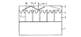
図1には本発明による有機半導体レーザーの基本的な構造が示されている。
・例えば打ち抜きないし型押し技術を用いた成形技法。
・光学的特性の変更方法、例えばホログラフィックな露光、この場合は活性材料か若しくは分離層を局所的に架橋結合させ、それによって溶媒に対して不活性化させる(写真技術)。
・ホログラフィックな露光方法、この場合材料の光学的特性が局所的に変更され、これは屈折率の変化を伴って現われる。
・例えば自己組織化による適切な量のナノ粒子の配列構成方法。
2 有機レーザー活性材料からなる層
3 透過性分離層
4 レーザー共振器
P ポンピング層
M モード
m=1 発光されたレーザー光
m=2 レーザー共振器によって反射されたレーザー光
Claims (16)
- 有機レーザー活性材料(2)からなる層とレーザー共振器(4)と光学的ポンプ源とを有する有機半導体レーザーであって、
前記光学的ポンプ源が、有機レーザー活性材料(2)からなる層と固定的に接続され、さらに前記有機レーザー活性材料(2)からなる層と1つのユニットを形成している有機半導体レーザーにおいて、
前記光学的ポンプ源が、電気的に作動される無機LED(1)であり、
前記有機レーザー活性材料(2)はビーム透過性の分離層(3)によって無機LEDから分離されており、
前記無機LED(1)の無機結晶はn>2の屈折率を有し、
前記有機レーザー活性材料(2)はn<2の屈折率を有し、
前記分離層(3)は、前記有機レーザー活性材料(2)の屈折率よりも小さい屈折率を有しており、
前記有機レーザー活性材料(2)に向いた側の前記無機LED(1)の表面は、フォトニック結晶の形態を有し、
前記無機LED(1)の第1の表面の表面輪郭が、有機レーザー材料(2)からなるレーザー活性層へ移行し、
前記レーザー共振器(4)が、前記無機LED(1)とは反対側の有機レーザー活性材料(2)の第2の表面と、前記第1の表面の前記レーザー活性層へ移行した表面輪郭との構造化によって形成されている、
ことを特徴とする有機半導体レーザー。 - 前記分離層(3)はプラスチック材料から形成されている、請求項1記載の有機半導体レーザー。
- 前記分離層(3)はテレフタル酸ポリエチレンから形成されている、請求項2記載の有機半導体レーザー。
- 前記レーザー共振器(4)は、前記分離層(3)と前記有機レーザー活性材料(2)の間の境界面に形成されている、請求項1から3までのいずれか1項記載の有機半導体レーザー。
- 前記有機レーザー活性材料(2)内で生じたモード(M)は前記レーザー共振器(4)の構造によって回折され、それによりモードの一部が反射され、フィードバックによって1つの光波の形成がされ、
前記モードの他の部分は、前記有機レーザー活性材料(2)の主伸長方向に対して垂直方向に放出される発光レーザー光を形成する、請求項1から4いずれか1項記載の有機半導体レーザー。 - 前記レーザー共振器(4)は、DFB(distributed feedback)共振器として形成されている、請求項1から5いずれか1項記載の有機半導体レーザー。
- ポンピング源の発光波長は有機レーザー活性材料(2)の吸収帯域に整合されている、請求項1から6いずれか1項記載の有機半導体レーザー。
- レーザー共振器(4)は、変調周期において勾配を有している深い格子構造を有している、請求項1から7いずれか1項記載の有機半導体レーザー。
- 周期的な構造を有しているレーザー共振器が複数の空間方向において形成されている、請求項1から8いずれか1項記載の有機半導体レーザー。
- 前記レーザー共振器は、四辺形又は六角形の格子状に形成されている、請求項9記載の有機半導体レーザー。
- 有機レーザー活性層(2)とレーザー共振器(4)とを有する有機半導体レーザーの製造方法であって、
光学的ポンプ源が有機レーザー活性材料(2)からなる層を備え、
前記光学的ポンプ源が、有機レーザー活性材料(2)からなる層と固定的に接続され、前記有機レーザー活性材料(2)からなる層と1つのユニットを形成しており、
前記光学的ポンプ源が、電気的に作動される無機LED(light emitting device)である有機半導体レーザーの製造方法において、
前記有機レーザー活性材料(2)をビーム透過性の分離層(3)によって前記無機LED(1)から分離し、
ここで前記無機LED(1)の無機結晶はn>2の屈折率を有し、
前記有機レーザー活性材料(2)はn<2の屈折率を有し、
前記分離層(3)は、前記有機レーザー活性材料(2)の屈折率よりも小さい屈折率を有しており、
前記有機レーザー活性材料(2)に向いた側の前記無機LED(1)の表面は、フォトニック結晶の形態を有し、
前記無機LED(1)の第1の表面の表面輪郭が、有機レーザー材料(2)からなるレーザー活性層へ移行し、
前記レーザー共振器(4)が、前記無機LED(1)とは反対側の有機レーザー活性材料(2)第2の表面と、前記第1の表面の前記レーザー活性層へ移行した表面輪郭との構造化によって形成される、
いることを特徴とする有機半導体レーザーの製造方法。 - 無機LED(1)の上に透過性分離層(3)または有機レーザー活性材料(2)層が析出手法によって被着される、請求項11記載の方法。
- 前記レーザー共振器(4)は有機レーザー活性層(2)の構造化によって製造され、
構造化部分の製造は機械的に行われる、請求項11または12記載の方法。 - 前記構造化は、打ち抜き加工によって行われる、請求項13記載の方法。
- 前記構造化は、ナノ粒子を自己組織化により配列することによって行われる、請求項11または12記載の方法。
- 前記レーザー共振器(4)を形成するための構造化部分の製造は、光学的及び/又は化学的手法によって行われる、請求項11または12記載の方法。
Applications Claiming Priority (4)
| Application Number | Priority Date | Filing Date | Title |
|---|---|---|---|
| DE102007003856 | 2007-01-25 | ||
| DE102007003856.0 | 2007-01-25 | ||
| DE102007011124A DE102007011124A1 (de) | 2007-01-25 | 2007-03-07 | Organischer Halbleiterlaser und Verfahren zu dessen Herstellung |
| DE102007011124.1 | 2007-03-07 |
Publications (3)
| Publication Number | Publication Date |
|---|---|
| JP2008182245A JP2008182245A (ja) | 2008-08-07 |
| JP2008182245A5 JP2008182245A5 (ja) | 2011-06-23 |
| JP5204498B2 true JP5204498B2 (ja) | 2013-06-05 |
Family
ID=39462027
Family Applications (1)
| Application Number | Title | Priority Date | Filing Date |
|---|---|---|---|
| JP2008014864A Expired - Fee Related JP5204498B2 (ja) | 2007-01-25 | 2008-01-25 | 有機半導体レーザー及びその製造方法 |
Country Status (4)
| Country | Link |
|---|---|
| US (1) | US7970036B2 (ja) |
| EP (1) | EP1950855B1 (ja) |
| JP (1) | JP5204498B2 (ja) |
| DE (1) | DE102007011124A1 (ja) |
Families Citing this family (3)
| Publication number | Priority date | Publication date | Assignee | Title |
|---|---|---|---|---|
| DE102014116613B4 (de) | 2014-11-13 | 2023-05-04 | Osram Oled Gmbh | Optoelektronische Vorrichtung, Verwendung eines dualen Emitters als Wellenlängenkonversionsstoff |
| WO2018043763A1 (en) | 2016-09-02 | 2018-03-08 | Kyushu University, National University Corporation | Continuous-wave organic thin-film distributed feedback laser and electrically driven organic semiconductor laser diode |
| WO2018147470A1 (en) | 2017-02-07 | 2018-08-16 | Kyushu University, National University Corporation | Current-injection organic semiconductor laser diode, method for producing same and program |
Family Cites Families (18)
| Publication number | Priority date | Publication date | Assignee | Title |
|---|---|---|---|---|
| US3969686A (en) * | 1975-03-26 | 1976-07-13 | Xerox Corporation | Beam collimation using multiple coupled elements |
| US5337328A (en) * | 1992-05-08 | 1994-08-09 | Sdl, Inc. | Semiconductor laser with broad-area intra-cavity angled grating |
| US5796771A (en) | 1996-08-19 | 1998-08-18 | The Regents Of The University Of California | Miniature self-pumped monolithically integrated solid state laser |
| US6330262B1 (en) * | 1997-05-09 | 2001-12-11 | The Trustees Of Princeton University | Organic semiconductor lasers |
| US5881089A (en) * | 1997-05-13 | 1999-03-09 | Lucent Technologies Inc. | Article comprising an organic laser |
| EP1044488A1 (de) * | 1997-12-31 | 2000-10-18 | Fraunhofer-Gesellschaft Zur Förderung Der Angewandten Forschung E.V. | Laser mit einem organischen emittermaterial und verteilter rückkopplung |
| DE19805993A1 (de) * | 1997-12-31 | 1999-07-08 | Fraunhofer Ges Forschung | Laser mit einem organischen Emittermaterial und verteilter Rückkoppelung |
| EP1035623A1 (en) * | 1998-12-04 | 2000-09-13 | Interuniversitair Micro-Elektronica Centrum Vzw | A device for emitting electromagnetic radiation and a method of producing such device |
| DE10064448A1 (de) * | 2000-12-22 | 2002-07-04 | Osram Opto Semiconductors Gmbh | Verfahren zum Aufrauhen eines Halbleiterchips für die Optoelektronik |
| US6879618B2 (en) | 2001-04-11 | 2005-04-12 | Eastman Kodak Company | Incoherent light-emitting device apparatus for driving vertical laser cavity |
| US6658037B2 (en) * | 2001-04-11 | 2003-12-02 | Eastman Kodak Company | Incoherent light-emitting device apparatus for driving vertical laser cavity |
| DE10162783A1 (de) * | 2001-12-19 | 2003-07-10 | Univ Dresden Tech | Elektrisch gepumpter Laser mit organischen Schichten |
| US6853660B2 (en) * | 2002-10-16 | 2005-02-08 | Eastman Kodak Company | Organic laser cavity arrays |
| US20040076204A1 (en) * | 2002-10-16 | 2004-04-22 | Kruschwitz Brian E. | External cavity organic laser |
| US7292614B2 (en) * | 2003-09-23 | 2007-11-06 | Eastman Kodak Company | Organic laser and liquid crystal display |
| EP1743197B1 (en) * | 2004-04-23 | 2011-08-10 | Olivier M. Parriaux | High efficiency optical diffraction device |
| DE102005048408B4 (de) | 2005-06-10 | 2015-03-19 | Osram Opto Semiconductors Gmbh | Dünnfilm-Halbleiterkörper |
| EP1906497B1 (de) | 2006-09-27 | 2011-01-05 | OSRAM Opto Semiconductors GmbH | Halbleiterlaservorrichtung und Verfahren zu deren Herstellung |
-
2007
- 2007-03-07 DE DE102007011124A patent/DE102007011124A1/de not_active Withdrawn
-
2008
- 2008-01-25 JP JP2008014864A patent/JP5204498B2/ja not_active Expired - Fee Related
- 2008-01-25 US US12/011,437 patent/US7970036B2/en not_active Expired - Fee Related
- 2008-01-25 EP EP08150667A patent/EP1950855B1/de active Active
Also Published As
| Publication number | Publication date |
|---|---|
| US20080187017A1 (en) | 2008-08-07 |
| DE102007011124A1 (de) | 2008-07-31 |
| US7970036B2 (en) | 2011-06-28 |
| JP2008182245A (ja) | 2008-08-07 |
| EP1950855A1 (de) | 2008-07-30 |
| EP1950855B1 (de) | 2011-06-22 |
Similar Documents
| Publication | Publication Date | Title |
|---|---|---|
| Khaidarov et al. | Control of LED emission with functional dielectric metasurfaces | |
| TWI712182B (zh) | 共振光學腔發光裝置 | |
| US20120320939A1 (en) | Laser light coupling into soi cmos photonic integrated circuit | |
| WO2012015990A2 (en) | Plasmon lasers at deep subwavelength scale | |
| KR102496476B1 (ko) | 전자기파 반사체 및 이를 포함하는 광학소자 | |
| Morales-Vidal et al. | Distributed feedback lasers based on perylenediimide dyes for label-free refractive index sensing | |
| CN103579901A (zh) | 表面发射激光器装置和原子振荡器 | |
| US10658539B2 (en) | Light emitting diode device | |
| WO2021241701A1 (ja) | 光学デバイスおよび発光デバイス | |
| JP5204498B2 (ja) | 有機半導体レーザー及びその製造方法 | |
| EP1793248B1 (en) | Waveguide and device including the same | |
| Kuramochi | Manipulating and trapping light with photonic crystals from fundamental studies to practical applications | |
| Foroutan‐Barenji et al. | Single‐mode lasing from a single 7 nm thick monolayer of colloidal quantum wells in a monolithic microcavity | |
| US20230378720A1 (en) | Vertical laser emitter and manufacturing method thereof | |
| Lin et al. | Vertical light-emitting diodes with surface gratings and rough surfaces for effective light extraction | |
| JP5217100B2 (ja) | 光学ユニット | |
| JP5818198B2 (ja) | 多光周波数発生光源 | |
| EP2692031B1 (fr) | Laser plasmonique et son procede de fabrication. | |
| KR101208109B1 (ko) | 파장 가변 필터 및 이를 이용한 파장 가변 외부 공진 레이저 | |
| JP2008182245A5 (ja) | ||
| US6574249B2 (en) | Thin film laser emitting device and method for the manufacture thereof | |
| US20070058688A1 (en) | End pumping vertical external cavity surface emitting laser | |
| Menon et al. | Photonic emitters and circuits based on colloidal quantum dot composites | |
| Mischok et al. | Lasing and Macroscopic Coherence of Hybridized Modes in Coupled 2D Waveguide‐VCSEL Resonators | |
| JP5077880B2 (ja) | 微細構造素子製造装置及び微細構造素子生産方法 |
Legal Events
| Date | Code | Title | Description |
|---|---|---|---|
| A621 | Written request for application examination |
Free format text: JAPANESE INTERMEDIATE CODE: A621 Effective date: 20101119 |
|
| RD04 | Notification of resignation of power of attorney |
Free format text: JAPANESE INTERMEDIATE CODE: A7424 Effective date: 20101227 |
|
| RD04 | Notification of resignation of power of attorney |
Free format text: JAPANESE INTERMEDIATE CODE: A7424 Effective date: 20101228 |
|
| A521 | Request for written amendment filed |
Free format text: JAPANESE INTERMEDIATE CODE: A523 Effective date: 20110502 |
|
| A977 | Report on retrieval |
Free format text: JAPANESE INTERMEDIATE CODE: A971007 Effective date: 20120928 |
|
| A131 | Notification of reasons for refusal |
Free format text: JAPANESE INTERMEDIATE CODE: A131 Effective date: 20121005 |
|
| A521 | Request for written amendment filed |
Free format text: JAPANESE INTERMEDIATE CODE: A523 Effective date: 20121228 |
|
| TRDD | Decision of grant or rejection written | ||
| A01 | Written decision to grant a patent or to grant a registration (utility model) |
Free format text: JAPANESE INTERMEDIATE CODE: A01 Effective date: 20130118 |
|
| A61 | First payment of annual fees (during grant procedure) |
Free format text: JAPANESE INTERMEDIATE CODE: A61 Effective date: 20130215 |
|
| R150 | Certificate of patent or registration of utility model |
Free format text: JAPANESE INTERMEDIATE CODE: R150 |
|
| FPAY | Renewal fee payment (event date is renewal date of database) |
Free format text: PAYMENT UNTIL: 20160222 Year of fee payment: 3 |
|
| S111 | Request for change of ownership or part of ownership |
Free format text: JAPANESE INTERMEDIATE CODE: R313111 |
|
| R350 | Written notification of registration of transfer |
Free format text: JAPANESE INTERMEDIATE CODE: R350 |
|
| R250 | Receipt of annual fees |
Free format text: JAPANESE INTERMEDIATE CODE: R250 |
|
| R250 | Receipt of annual fees |
Free format text: JAPANESE INTERMEDIATE CODE: R250 |
|
| LAPS | Cancellation because of no payment of annual fees |