JP5204498B2 - Organic semiconductor laser and manufacturing method thereof - Google Patents
Organic semiconductor laser and manufacturing method thereof Download PDFInfo
- Publication number
- JP5204498B2 JP5204498B2 JP2008014864A JP2008014864A JP5204498B2 JP 5204498 B2 JP5204498 B2 JP 5204498B2 JP 2008014864 A JP2008014864 A JP 2008014864A JP 2008014864 A JP2008014864 A JP 2008014864A JP 5204498 B2 JP5204498 B2 JP 5204498B2
- Authority
- JP
- Japan
- Prior art keywords
- laser
- organic
- active material
- layer
- resonator
- Prior art date
- Legal status (The legal status is an assumption and is not a legal conclusion. Google has not performed a legal analysis and makes no representation as to the accuracy of the status listed.)
- Expired - Fee Related
Links
Images


Classifications
-
- H—ELECTRICITY
- H01—ELECTRIC ELEMENTS
- H01S—DEVICES USING THE PROCESS OF LIGHT AMPLIFICATION BY STIMULATED EMISSION OF RADIATION [LASER] TO AMPLIFY OR GENERATE LIGHT; DEVICES USING STIMULATED EMISSION OF ELECTROMAGNETIC RADIATION IN WAVE RANGES OTHER THAN OPTICAL
- H01S3/00—Lasers, i.e. devices using stimulated emission of electromagnetic radiation in the infrared, visible or ultraviolet wave range
- H01S3/14—Lasers, i.e. devices using stimulated emission of electromagnetic radiation in the infrared, visible or ultraviolet wave range characterised by the material used as the active medium
- H01S3/16—Solid materials
- H01S3/168—Solid materials using an organic dye dispersed in a solid matrix
-
- H—ELECTRICITY
- H01—ELECTRIC ELEMENTS
- H01S—DEVICES USING THE PROCESS OF LIGHT AMPLIFICATION BY STIMULATED EMISSION OF RADIATION [LASER] TO AMPLIFY OR GENERATE LIGHT; DEVICES USING STIMULATED EMISSION OF ELECTROMAGNETIC RADIATION IN WAVE RANGES OTHER THAN OPTICAL
- H01S3/00—Lasers, i.e. devices using stimulated emission of electromagnetic radiation in the infrared, visible or ultraviolet wave range
- H01S3/09—Processes or apparatus for excitation, e.g. pumping
- H01S3/091—Processes or apparatus for excitation, e.g. pumping using optical pumping
- H01S3/0915—Processes or apparatus for excitation, e.g. pumping using optical pumping by incoherent light
- H01S3/0933—Processes or apparatus for excitation, e.g. pumping using optical pumping by incoherent light of a semiconductor, e.g. light emitting diode
-
- H—ELECTRICITY
- H01—ELECTRIC ELEMENTS
- H01S—DEVICES USING THE PROCESS OF LIGHT AMPLIFICATION BY STIMULATED EMISSION OF RADIATION [LASER] TO AMPLIFY OR GENERATE LIGHT; DEVICES USING STIMULATED EMISSION OF ELECTROMAGNETIC RADIATION IN WAVE RANGES OTHER THAN OPTICAL
- H01S3/00—Lasers, i.e. devices using stimulated emission of electromagnetic radiation in the infrared, visible or ultraviolet wave range
- H01S3/05—Construction or shape of optical resonators; Accommodation of active medium therein; Shape of active medium
- H01S3/06—Construction or shape of active medium
- H01S3/063—Waveguide lasers, i.e. whereby the dimensions of the waveguide are of the order of the light wavelength
- H01S3/0632—Thin film lasers in which light propagates in the plane of the thin film
- H01S3/0635—Thin film lasers in which light propagates in the plane of the thin film provided with a periodic structure, e.g. using distributed feed-back, grating couplers
Description
本発明は、有機レーザー活性材料からなる層とレーザー共振器と光学的ポンプ源とを有する有機半導体レーザーであって、前記光学的ポンプ源が、有機レーザー活性材料からなる層と固定的に接続され、さらに前記有機レーザー活性材料からなる層と1つのユニットを形成している有機半導体レーザーに関している。 The present invention is an organic semiconductor laser having a layer and a laser resonator and an optical pump source consisting of an organic laser-active material, the optical pump source is fixedly connected to the layer composed of the organic laser-active material Furthermore, the present invention relates to an organic semiconductor laser forming one unit with a layer made of the organic laser active material .
有機半導体は、スペクトル調整可能なレーザーにおける活性材料として非常に簡単にかつ低コストで利用できるものである。有機活性材料として通常はポリマーや小分子が用いられている。そのため適切な外部レーザー源を用いた光学的な励起のもとではレーザーの作動が可視スペクトル領域全体において可能である。有機半導体の直接の電気的な励起は、電荷担体移動度の少なさとその結果としての荷電された半導体フィルムにおける吸収量に基づいてこれまでは示すことができなかった。これまでのレーザー励起ではいつも多くのスペースを必要とする高価な外部レーザー源を介して行われてきた。
それ故に本発明の基礎とする課題は、高いコストと多くのスペースが必要な外部レーザー源なしで有機半導体レーザーを励起させ得る手段とそのような有機半導体の製造方法を提供することである。 Therefore, the problem underlying the present invention is to provide means capable of exciting an organic semiconductor laser without an external laser source requiring high cost and a lot of space, and a method for producing such an organic semiconductor.
前記課題は本発明により、前記光学的ポンプ源が、電気的に作動される無機LED(1)であり、前記有機レーザー活性材料はビーム透過性の分離層によって無機LEDから分離されており、前記無機LEDの無機結晶はn>2の屈折率を有し、前記有機レーザー活性材料はn<2の屈折率を有し、前記分離層は、前記有機レーザー活性材料の屈折率よりも小さい屈折率を有しており、前記有機レーザー活性材料に向いた側の前記無機LEDの表面は、フォトニック結晶の形態を有し、前記無機LEDの第1の表面の表面輪郭が、有機レーザー材料からなるレーザー活性層へ移行し、前記レーザー共振器が、前記無機LEDとは反対側の有機レーザー活性材料あの第2の表面と、前記第1の表面の前記レーザー活性層へ移行した表面輪郭との構造化によって形成されている有機半導体レーザーによって解決される。 The object is according to the present invention, wherein the optical pump source is an electrically operated inorganic LED ( 1 ), wherein the organic laser active material is separated from the inorganic LED by a beam transmissive separating layer, The inorganic crystal of the inorganic LED has a refractive index of n> 2, the organic laser active material has a refractive index of n <2, and the separation layer has a refractive index smaller than the refractive index of the organic laser active material. The surface of the inorganic LED on the side facing the organic laser active material has a form of a photonic crystal, and the surface contour of the first surface of the inorganic LED is made of an organic laser material. Transition to a laser active layer, wherein the laser resonator has a second surface of the organic laser active material opposite the inorganic LED, and a surface profile of the first surface transitioned to the laser active layer; Is solved by an organic semiconductor laser is formed by structuring.
有機半導体の少なくとも1つの実施形態によれば、この有機半導体は有機的レーザー活性材料からなる少なくとも1つの層とレーザー共振器を含み、光学的ポンプ源がこの有機半導体レーザーと一体的に接続されている。 According to at least one embodiment of the organic semiconductor, the organic semiconductor includes at least one layer of organic laser active material and a laser resonator, and an optical pump source is integrally connected to the organic semiconductor laser. Yes.
換言すればポンプ源が有機半導体レーザーとモノリシックに接続されている。すなわちポンプ源と有機半導体レーザーは有利には相互に固定的に接続されて1つのユニットを形成している。 In other words, the pump source is connected monolithically with the organic semiconductor laser. That is, the pump source and the organic semiconductor laser are preferably fixedly connected to each other to form a unit.
有機半導体レーザーの別の少なくとも1つの実施形態によれば、光学的ポンプ源が電気的に励起される無機LED(light emitting device; 発光デバイス)からなっているか若しくは含んでいる。有機レーザーと励起源との直接的でかつモノリシックな結合によってこれまでの光学的ポンプ源に要していたコストが削減できる。この有機半導体レーザーの製造は有利にはこれまでの無機LEDの製造に用いられていたチッププロセスの拡張として行われる。ポンプ源は唯1つの無機LEDを含んでいてもよいし、複数の例えば少なくとも2つの無機LEDを含んでいてもよい。LEDは、LED半導体チップであってもよい。すなわちこのLED半導体チップは有機半導体レーザーと一体的に接続され得るものである。 According to another at least one embodiment of the organic semiconductor laser, the optical pump source consists or comprises an electrically excited inorganic LED (light emitting device). The direct and monolithic coupling between the organic laser and the excitation source can reduce the cost of previous optical pump sources. The production of this organic semiconductor laser is advantageously carried out as an extension of the chip process used in the production of inorganic LEDs so far. The pump source may include only one inorganic LED or may include a plurality of, for example, at least two inorganic LEDs. The LED may be an LED semiconductor chip. That is, the LED semiconductor chip can be connected integrally with the organic semiconductor laser.
別の有利な実施形態によれば、半導体共振器が有機レーザー活性材料の表面の構造化によって形成される。 According to another advantageous embodiment, the semiconductor resonator is formed by structuring the surface of the organic laser active material.
このレーザー活性材料表面の所期の構造化によれば、いわゆるDFB(distributed feedback;分布帰還型)共振器が作成できる。 According to the desired structuring of the surface of the laser active material, a so-called DFB (distributed feedback) resonator can be created.
DFB共振器形成のための構造化された表面の形成は、表面に対して垂直方向でのレーザー発光に対しては上側若しくは下側に形成されてもよいし、表面に対して側方方向でのレーザー発光に対しては側方に形成されてもよい。 The formation of the structured surface for forming the DFB resonator may be formed on the upper side or the lower side for laser emission in a direction perpendicular to the surface, or in a lateral direction with respect to the surface. It may be formed laterally with respect to the laser emission.
さらなる別の有利な構成例によれば、有機レーザー活性材料がビーム透過性の分離層によって無機LEDから分離される。この場合分離層は少なくとも無機LEDによって生成されるポンピングビームの一部に対して透過性である。分離層は有利には無機LED内で生成されるポンピングビームに対して透過性である。 According to yet another advantageous configuration, the organic laser active material is separated from the inorganic LED by a beam transmissive separating layer. In this case, the separation layer is transparent to at least a part of the pumping beam produced by the inorganic LED. The separating layer is preferably transparent to the pumping beam produced in the inorganic LED.
この分離層は、無機LEDから有機活性材料へのフォトンの実質的に無損失の入力結合を可能にする。 This separation layer allows a substantially lossless input coupling of photons from the inorganic LED to the organic active material.
透過性の分離層を利用した場合には、この透過性分離層と有機レーザー活性材料との間の境界層にもレーザー共振器を形成することが可能である。 When a transmissive separation layer is used, a laser resonator can also be formed in the boundary layer between the transmissive separation layer and the organic laser active material.
さらに有利な構成例によれば、無機LEDの表面が粗面に形成される。この無機LED表面の粗面仕上げは無機LEDの外的影響を高める。このケースでは分離層を平坦化層として用いることも有利である。すなわちこの場合は分離層がその光学的特性の他に、例えば粗面仕上げされた無機LED表面の平坦化にも用いられる。 According to a further advantageous configuration example, the surface of the inorganic LED is formed into a rough surface. This rough surface finish of the inorganic LED increases the external influence of the inorganic LED. In this case, it is also advantageous to use the separation layer as a planarization layer. That is, in this case, the separation layer is used for flattening the surface of an inorganic LED having a rough surface, for example, in addition to its optical characteristics.
平坦化層の被着は有利にはスピンコーティングや凹版印刷のようなコーティングプロセスによって行われる。 The planarization layer is preferably applied by a coating process such as spin coating or intaglio printing.
本発明のさらに有利な構成例によれば、無機LEDの表面がフォトニック結晶の形態に形成される。換言すれば、有機材料に向いている無機LED表面がフォトニック結晶の形態を有しているか又はフォトニック結晶の形式に従って構造化される。そのように形成された表面を有するLEDは例えば国際公開第2006/131087号パンフレットに記載されており、したがってこれに関する開示内容は参照として本明細書にも含まれるものとする。 According to a further advantageous configuration example of the present invention, the surface of the inorganic LED is formed in the form of a photonic crystal. In other words, the inorganic LED surface facing the organic material has the form of a photonic crystal or is structured according to the form of the photonic crystal. LEDs having a surface so formed are described, for example, in WO 2006/31087, the disclosure of which is hereby incorporated by reference.
有利にはさらなる層が蒸着法や真空蒸着法のような析出手法を介して生成され、それによってフォトニック結晶の表面輪郭がさらなる層へ移行され、有機レーザーに整合されたDFB共振器が形成される。 An additional layer is advantageously generated via a deposition technique such as vapor deposition or vacuum vapor deposition, whereby the surface profile of the photonic crystal is transferred to the additional layer, forming an organic laser matched DFB resonator. The
さらに有利な構成例によれば、無機LEDの発光波長が有機レーザー活性材料の吸収スパンに整合される。 According to a further advantageous configuration, the emission wavelength of the inorganic LED is matched to the absorption span of the organic laser active material.
この整合により、無機LEDの励起エネルギーが有機レーザー活性材料内に注入される。 Due to this matching, the excitation energy of the inorganic LED is injected into the organic laser active material.
本発明のさらに別の有利な実施例によれば、レーザー共振器が変調周期において勾配を有している深い格子構造を有する。そのようなレーザー共振器は例えば刊行物"A nearly diffraction limited surface emitting conjugated polymer laser utilizing a two-dimensional photonic band structure, S.Riechel et al., Applied Physics Letters, Volume 77, Number 15, pp 2310-2312"に記載があり、ここに紹介されているレーザーに関する開示内容が参照される。この構成によって発光波長がチップ面に亘り空間的に変化する整合可能なレーザー源の製造が可能となる。有機レーザーのビーム品質の向上のために有利には、変調が複数の空間方向に向けて、例えば四辺形若しくは六角形の格子状に実施される。 According to a further advantageous embodiment of the invention, the laser resonator has a deep grating structure with a gradient in the modulation period. Such laser resonator, for example publication "A nearly diffraction limited surface emitting conjugated polymer laser utilizing a two-dimensional photonic band structure, S.Riechel et al., Applied Physics Le t ters, Volume 77, Number 15, pp 2310 -2312 "and reference is made to the disclosures relating to lasers introduced herein. With this configuration, it is possible to manufacture an alignable laser source in which the emission wavelength varies spatially across the chip surface. In order to improve the beam quality of the organic laser, the modulation is preferably carried out in a plurality of spatial directions, for example in the form of a quadrilateral or hexagonal lattice.
代替的な実施例によれば僅かな変調深度も選択可能である。これによりチップ面全体に亘って効果的に分散された共振器が延在し、それによって単一モードに回折制限されたコヒーレンスな発光が得られるようになる。そのようなレーザー共振器は例えば刊行物"Very compact tunable solid-state laser utilizing a thin-film organic semiconductor, S. Riechel et al., Optics Letters, Vol 26, No 9, pp 593-595"に記載があり、ここに紹介されているレーザーに関する開示内容が参照される。 According to an alternative embodiment, a small modulation depth can be selected. This extends resonators that are effectively distributed over the entire chip surface, thereby providing coherence emission that is diffraction limited to a single mode. Such laser resonator, for example publication "Very compact tunable solid-state laser utilizing a thin-film organic semiconductor, S. Riechel et al., Optics Le t ters, Vol 26, No 9, pp 593-595" in There is a description and reference is made to the disclosures relating to lasers introduced herein.
レーザー共振器を生成するための有機レーザー活性材料の構造化は鋳造に応じて機械的に又は光学的ないし化学的に行うことが可能である。 The structuring of the organic laser active material to produce the laser resonator can be done mechanically or optically or chemically depending on the casting.
有機レーザー活性層とレーザー共振器とを有する有機半導体レーザーの製造方法に関しては、電気的に作動可能な無機LEDがレーザー活性材料からなる有機層を備えることによって前記課題が解決される。 With regard to a method for producing an organic semiconductor laser having an organic laser active layer and a laser resonator, the above problem is solved by providing an electrically operable inorganic LED comprising an organic layer made of a laser active material.
有利には、無機LEDへのさらなる層の被着、例えば透過性分離層若しくはレーザー活性材料からなる有機層の被着が析出手法によって行われる。 Advantageously, a further layer is applied to the inorganic LED, for example a transmissive separating layer or an organic layer made of a laser active material, by a deposition technique.
レーザー共振器の製造は有機層の構造化によって行われており、有利には機械的に例えば打ち抜き加工によってまたは光学的ないし化学的に行われる。 The laser resonator is manufactured by structuring the organic layer, preferably mechanically, for example by stamping or optically or chemically.
レーザー共振器の構造化はポンピング源の構造化を介して行ってもよい。例えばさらなる層が無機LEDの構造化された表面に被着されるならば、それと共にレーザー共振器の構造部が自動的に無機層表面に形成されるようになる。 The structuring of the laser resonator may be performed via the structuring of the pumping source. For example, if a further layer is applied to the structured surface of the inorganic LED, a laser cavity structure is automatically formed on the inorganic layer surface with it.
本発明のさらなる利点は従属請求項並びに以下の明細書でも開示されている。 Further advantages of the invention are disclosed in the dependent claims as well as in the following specification.
以下では本発明の実施例を図面に基づいて詳細に説明する。
図1には本発明による有機半導体レーザーの基本的な構造が示されている。
Hereinafter, embodiments of the present invention will be described in detail with reference to the drawings.
FIG. 1 shows the basic structure of an organic semiconductor laser according to the present invention.
従来型の無機LED1は有機レーザー活性材料2からなる層を備えている。無機LED1が電気的に作動されると、その表面から光が有機レーザー活性材料2からなる層の中へ発光される。この有機レーザー活性材料からなる層は複数の有機層ないしは有機フィルムからなっている。
The conventional
無機LED1と有機レーザー活性材料2からなる層の間には透明な分離層3が設けられている。この分離層3は、無機LEDから有機活性材料へのフォトンの無損失の入力結合を可能にする。
A
無機結晶(n>2)と有機材料(n<2)の間の屈折率の差に基づいてこの分離層はモードガイドのためにも大きな意義を持っている。この分離層3は有機材料2の屈折率よりも小さな屈折率を有しており、この屈折率の差が無機LEDからのレーザーモードの効果的な入力結合を可能にしている。それによって特に有機活性材料へのレーザーモードの誘導が良好になされ、光学的な増幅が行われる。
Based on the difference in refractive index between the inorganic crystal (n> 2) and the organic material (n <2), this separation layer has great significance for the mode guide. The
この分離層は、例えばテレフタル酸ポリエチレン(PET)などのプラスチック材料から形成されていてもよいしそのような材料を含んだものでもよい。 This separation layer may be made of a plastic material such as polyethylene terephthalate (PET), or may contain such a material.
この分離層は中心的な意味合いをもつものではあるが、必ずしも本発明の必須の構成要素というわけではない。 Although this separation layer has a central meaning, it is not necessarily an essential component of the present invention.
有機活性材料の層の厚みは、有機膜の内部へ案内されるモードが伝播され得るように構成される。 The thickness of the layer of organic active material is configured such that a guided mode can be propagated into the organic film.
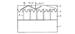
レーザー共振器4の形成のために、有機活性材料の表面は平面的ではなく次のように構造化される。すなわち周期的な隆起部分において案内されたモードの一部が面反射され、分散されたいわゆるDFB(distributed feedback)共振器が形成されるように行われる。
For the formation of the
無機LED1によっていわゆるポンピング光Pが有機レーザー活性材料2の励起のために送出される。
So-called pumping light P is sent out by the
このポンピング光Pは透過性の分離層3を透過してレーザー共振器4に入射する。
The pumping light P passes through the
有機レーザー活性材料内で生じたモードMはレーザー共振器4の構造によって回折される。それによりモードの一部m=2は反射されフィードバックによって1つの光波の形成が生じる。
The mode M generated in the organic laser active material is diffracted by the structure of the
他の部分m=1は、ここに示されている二次のDFB共振器の表面に対して垂直方向に放出される発光レーザー光を形成している。 The other part m = 1 forms an emitted laser beam that is emitted in a direction perpendicular to the surface of the secondary DFB resonator shown here.
図1による実施例の場合にはDFB構造部、すなわちDFB共振器が、分離層3とレーザー活性材料2の間に形成されている。
In the case of the embodiment according to FIG. 1, a DFB structure, ie a DFB resonator, is formed between the
また図には示していないが別の実施例としてDFB構造部をレーザー活性材料2の上側に設けることも可能である。
Although not shown in the drawing, as another example, a DFB structure can be provided on the upper side of the laser
さらにまたDFB構造部は一次のDFB共振器として構成されていてもよい。その場合にはレーザービームの放射が縁部、すなわち側方で行われる。一次のDFB共振器の主な利点はレーザービームの低減が出力結合損失の少なさに基づく点である。 Furthermore, the DFB structure may be configured as a primary DFB resonator. In that case, the radiation of the laser beam takes place at the edge, ie the side. The main advantage of the primary DFB resonator is that the laser beam reduction is based on low output coupling loss.
図2には本発明によるレーザー源の代替的な実施形態が示されている。無機LED1はここでは粗面仕上げされた表面を備えている。無機LEDの粗面状の表面は外的作用を高める。このことは例えば次のようなことに還元させることが可能である。すなわち無機LEDから出射されたビームの全反射に対する確率を粗面に基づいて低減させることである。
FIG. 2 shows an alternative embodiment of a laser source according to the present invention. Here, the
このケースでは分離層3を同時に平坦化層として用いることも可能である。
In this case, the
分離層3の被着に対しては有利には次のようなコーティングプロセス、例えばスピンコーティングプロセスや凹版印刷プロセスなどが適している。
For the deposition of the
これらのコーティングプロセスにおいては、所望の材料が溶媒の中で溶解され、その後で液状化フェーズから処理される。 In these coating processes, the desired material is dissolved in a solvent and then processed from the liquefaction phase.
DFB共振器ないしレーザー共振器4を、分離層3とレーザー活性材料2の間の境界面に形成するのか、あるいは有機レーザー活性材料2表面に形成するのかに関する概念的発端は、平坦化とは無関係のままである。
The conceptual origin of whether the DFB resonator or
図3には、本発明のさらに別の実施形態が示されている。 FIG. 3 shows yet another embodiment of the present invention.
この図3による実施形態では、光の出力結合の増大のために、無機LEDの表面がフォトニック結晶の形態に形成されている。表面の適切なフォトニック結晶構造のもとでは、つまり格子周期や変調深度の適切な構成のもとでは、フォトニック結晶は、LEDの方向性と出力結合効果を著しく高める。 In the embodiment according to FIG. 3, the surface of the inorganic LED is formed in the form of a photonic crystal in order to increase the output coupling of light. Under an appropriate photonic crystal structure on the surface, that is, under an appropriate configuration of lattice period and modulation depth, the photonic crystal significantly enhances the directionality and output coupling effect of the LED.
さらなる層に対する析出手法、例えば蒸着法や真空蒸着法などの適切な選択のもとに、無機LEDの表面における表面輪郭がフォトニック結晶の形態でさらなる層へ移行され、それによって有機レーザーに合わせたDFB共振器が形成される。 With appropriate choices such as deposition techniques for further layers, e.g. vapor deposition or vacuum deposition, the surface contour on the surface of the inorganic LED is transferred to the further layer in the form of a photonic crystal, thereby tailored to the organic laser A DFB resonator is formed.
無機LED表面にフォトニック結晶構造の形態でさらなる層を被着させることによって、有機レーザー活性材料2の上側ないし下側にDFB共振器が自動的に形成される。
By depositing a further layer in the form of a photonic crystal structure on the inorganic LED surface, a DFB resonator is automatically formed above or below the organic laser
全ての実施形態において有利なことは、無機LEDの発光波長を有機レーザー活性材料の吸収帯域に整合させることである。それにより無機LEDの励起エネルギーが活性材料に注入される。 In all embodiments, it is advantageous to match the emission wavelength of the inorganic LED to the absorption band of the organic laser active material. Thereby, the excitation energy of the inorganic LED is injected into the active material.
3つの実施形態の全てにおいては結合特性とそれに伴う共振器の有効長さが周期的構造の変調深度ないし変調レベルに応じて変化する。 In all three embodiments, the coupling characteristics and the associated effective resonator length vary depending on the modulation depth or modulation level of the periodic structure.
例えば変調周期に勾配を有している深い格子構造が用いられている場合には、発光波長がチップ面に亘り空間的に変化する整合可能なレーザー源が可能となる。 For example, when a deep grating structure having a gradient in the modulation period is used, a matchable laser source in which the emission wavelength varies spatially across the chip surface is possible.
有機レーザーのビーム品質の向上のために有利には、変調が複数の空間方向において、例えば四辺形ないし六角形の格子状に実施される。 In order to improve the beam quality of the organic laser, the modulation is preferably carried out in a plurality of spatial directions, for example in the form of a quadrilateral or hexagonal lattice.
それに対して僅かな変調深度は、チップ面全体に亘って効果的に分散された共振器の延在を生ぜしめ、それによって単一モードに回折制限されたコヒーレンスな発光が得られるようになる。 In contrast, a slight modulation depth results in the extension of resonators that are effectively distributed over the entire chip surface, thereby providing coherence emission that is diffraction limited to a single mode.
共振器形成のための無機LEDないし有機レーザー活性層の表面の構造化は前述したようにフォトニック結晶構造へのさらなる層の被着によって、あるいは機械的若しくは光学的/化学的に行われ得る。 The structuring of the surface of the inorganic LED or organic laser active layer for the formation of the resonator can be effected by applying further layers to the photonic crystal structure as described above, or mechanically or optically / chemically.
例示的に以下のさらなる方法が挙げられる。すなわち
・例えば打ち抜きないし型押し技術を用いた成形技法。
・光学的特性の変更方法、例えばホログラフィックな露光、この場合は活性材料か若しくは分離層を局所的に架橋結合させ、それによって溶媒に対して不活性化させる(写真技術)。
・ホログラフィックな露光方法、この場合材料の光学的特性が局所的に変更され、これは屈折率の変化を伴って現われる。
・例えば自己組織化による適切な量のナノ粒子の配列構成方法。
Illustrative examples include the following additional methods. Ie
- For example molding technique using a punching or embossing technology.
A method of changing the optical properties, for example holographic exposure, in this case the active material or the separating layer is locally cross-linked and thereby deactivated with respect to the solvent (photographic technique) .
A holographic exposure method, in which case the optical properties of the material are locally altered, which appears with a change in the refractive index .
A method of arranging an appropriate amount of nanoparticles , for example by self-assembly
図1〜図3による実施例によって表されたような本発明によれば省スペース的でかつ低コストなレーザー源が製造できる。レーザー共振器の幾何学構造と有機材料の選択の際の多様性に基づいてレーザー発光がこれらの考察のもとに任意に選択可能な波長のもとで全ての可視スペクトル領域に亘って実現できる。従って本発明はスペクトロスコープの分野においてもディスプレイ分野においても中心的な意義をなすものとなる。 According to the invention as represented by the embodiment according to FIGS. 1 to 3, a space-saving and low-cost laser source can be produced. Based on the laser resonator geometry and the diversity in the choice of organic materials, laser emission can be realized over the entire visible spectral region under any arbitrarily selectable wavelength based on these considerations. . Therefore, the present invention has a central significance both in the spectroscope field and in the display field.
本願は、ドイツ連邦共和国特許出願第102007003856.0号及び102007011124.1号の優先権を主張するものであり、その開示内容は参照により本願に取り入れられる。 The present application claims the priority of German patent applications 102007003856.0 and 1020070111244.1, the disclosure of which is incorporated herein by reference.
なお本発明は実施例に基づいたこれまでの説明によって限定されるものではないことを述べておく。むしろ本発明はあらゆる新規の特徴並びにそれらの特徴のあらゆる組み合わせを含むものであり、これには殊に特許請求の範囲に記載した特徴のあらゆる組み合わせが含まれる。このことはこのような特徴またはこのような組み合わせ自体が特許請求の範囲あるいは実施例に明示的には記載されていない場合であっても当てはまる。 It should be noted that the present invention is not limited to the above description based on the embodiments. Rather, the invention includes any novel features and combinations of those features, including in particular any combination of the features recited in the claims. This is true even if such features or such combinations themselves are not expressly recited in the claims or examples.
1 無機LED
2 有機レーザー活性材料からなる層
3 透過性分離層
4 レーザー共振器
P ポンピング層
M モード
m=1 発光されたレーザー光
m=2 レーザー共振器によって反射されたレーザー光
1 Inorganic LED
2 Layer made of organic laser
Claims (16)
前記光学的ポンプ源が、有機レーザー活性材料(2)からなる層と固定的に接続され、さらに前記有機レーザー活性材料(2)からなる層と1つのユニットを形成している有機半導体レーザーにおいて、
前記光学的ポンプ源が、電気的に作動される無機LED(1)であり、
前記有機レーザー活性材料(2)はビーム透過性の分離層(3)によって無機LEDから分離されており、
前記無機LED(1)の無機結晶はn>2の屈折率を有し、
前記有機レーザー活性材料(2)はn<2の屈折率を有し、
前記分離層(3)は、前記有機レーザー活性材料(2)の屈折率よりも小さい屈折率を有しており、
前記有機レーザー活性材料(2)に向いた側の前記無機LED(1)の表面は、フォトニック結晶の形態を有し、
前記無機LED(1)の第1の表面の表面輪郭が、有機レーザー材料(2)からなるレーザー活性層へ移行し、
前記レーザー共振器(4)が、前記無機LED(1)とは反対側の有機レーザー活性材料(2)の第2の表面と、前記第1の表面の前記レーザー活性層へ移行した表面輪郭との構造化によって形成されている、
ことを特徴とする有機半導体レーザー。 An organic semiconductor laser having a layer made of an organic laser active material (2), a laser resonator (4), and an optical pump source,
In the organic semiconductor laser, the optical pump source is fixedly connected to the layer made of the organic laser active material (2), and further forms one unit with the layer made of the organic laser active material (2).
The optical pump source is an electrically operated inorganic LED ( 1 );
The organic laser active material (2) is separated from the inorganic LED by a beam transmissive separation layer (3),
The inorganic crystal of the inorganic LED (1) has a refractive index of n> 2.
The organic laser active material (2) has a refractive index of n <2,
The separation layer (3) has a refractive index smaller than the refractive index of the organic laser active material (2) ,
The surface of the inorganic LED (1) on the side facing the organic laser active material (2) has the form of a photonic crystal,
The surface contour of the first surface of the inorganic LED (1) is transferred to the laser active layer made of the organic laser material (2),
The laser resonator (4) has a second surface of the organic laser active material (2) opposite to the inorganic LED (1) and a surface contour transferred to the laser active layer of the first surface; Formed by structuring ,
An organic semiconductor laser characterized by that.
前記モードの他の部分は、前記有機レーザー活性材料(2)の主伸長方向に対して垂直方向に放出される発光レーザー光を形成する、請求項1から4いずれか1項記載の有機半導体レーザー。5. The organic semiconductor laser according to claim 1, wherein the other part of the mode forms a light emitting laser beam that is emitted in a direction perpendicular to a main extension direction of the organic laser active material. .
光学的ポンプ源が有機レーザー活性材料(2)からなる層を備え、
前記光学的ポンプ源が、有機レーザー活性材料(2)からなる層と固定的に接続され、前記有機レーザー活性材料(2)からなる層と1つのユニットを形成しており、
前記光学的ポンプ源が、電気的に作動される無機LED(light emitting device)である有機半導体レーザーの製造方法において、
前記有機レーザー活性材料(2)をビーム透過性の分離層(3)によって前記無機LED(1)から分離し、
ここで前記無機LED(1)の無機結晶はn>2の屈折率を有し、
前記有機レーザー活性材料(2)はn<2の屈折率を有し、
前記分離層(3)は、前記有機レーザー活性材料(2)の屈折率よりも小さい屈折率を有しており、
前記有機レーザー活性材料(2)に向いた側の前記無機LED(1)の表面は、フォトニック結晶の形態を有し、
前記無機LED(1)の第1の表面の表面輪郭が、有機レーザー材料(2)からなるレーザー活性層へ移行し、
前記レーザー共振器(4)が、前記無機LED(1)とは反対側の有機レーザー活性材料(2)第2の表面と、前記第1の表面の前記レーザー活性層へ移行した表面輪郭との構造化によって形成される、
いることを特徴とする有機半導体レーザーの製造方法。 A method for producing an organic semiconductor laser having an organic laser active layer (2) and a laser resonator (4),
The optical pump source comprises a layer of organic laser active material (2);
The optical pump source is fixedly connected to a layer made of the organic laser active material (2) and forms a unit with the layer made of the organic laser active material (2) ;
Said optical pump source, the electrically actuated inorganic LED (light emitting device) manufacturing method of an organic semiconductor laser Ru der,
Separating the organic laser active material (2) from the inorganic LED (1) by a beam transmissive separation layer (3);
Here, the inorganic crystal of the inorganic LED (1) has a refractive index of n> 2.
The organic laser active material (2) has a refractive index of n <2,
The separation layer (3) has a refractive index smaller than the refractive index of the organic laser active material (2),
The surface of the inorganic LED (1) on the side facing the organic laser active material (2) has the form of a photonic crystal,
The surface contour of the first surface of the inorganic LED (1) is transferred to the laser active layer made of the organic laser material (2),
The laser resonator (4) includes an organic laser active material (2) second surface opposite to the inorganic LED (1), and a surface contour transferred to the laser active layer on the first surface. Formed by structuring ,
A method for producing an organic semiconductor laser.
構造化部分の製造は機械的に行われる、請求項11または12記載の方法。 The laser resonator (4) is manufactured by structuring the organic laser active layer (2) ,
13. A method according to claim 11 or 12 , wherein the manufacture of the structured part is performed mechanically .
Applications Claiming Priority (4)
| Application Number | Priority Date | Filing Date | Title |
|---|---|---|---|
| DE102007003856.0 | 2007-01-25 | ||
| DE102007003856 | 2007-01-25 | ||
| DE102007011124A DE102007011124A1 (en) | 2007-01-25 | 2007-03-07 | Organic semiconductor laser and process for its production |
| DE102007011124.1 | 2007-03-07 |
Publications (3)
| Publication Number | Publication Date |
|---|---|
| JP2008182245A JP2008182245A (en) | 2008-08-07 |
| JP2008182245A5 JP2008182245A5 (en) | 2011-06-23 |
| JP5204498B2 true JP5204498B2 (en) | 2013-06-05 |
Family
ID=39462027
Family Applications (1)
| Application Number | Title | Priority Date | Filing Date |
|---|---|---|---|
| JP2008014864A Expired - Fee Related JP5204498B2 (en) | 2007-01-25 | 2008-01-25 | Organic semiconductor laser and manufacturing method thereof |
Country Status (4)
| Country | Link |
|---|---|
| US (1) | US7970036B2 (en) |
| EP (1) | EP1950855B1 (en) |
| JP (1) | JP5204498B2 (en) |
| DE (1) | DE102007011124A1 (en) |
Families Citing this family (3)
| Publication number | Priority date | Publication date | Assignee | Title |
|---|---|---|---|---|
| DE102014116613B4 (en) | 2014-11-13 | 2023-05-04 | Osram Oled Gmbh | Optoelectronic device using a dual emitter as wavelength conversion material |
| US11539190B2 (en) * | 2016-09-02 | 2022-12-27 | Kyushu University, National University Corporation | Continuous-wave organic thin-film distributed feedback laser and electrically driven organic semiconductor laser diode |
| EP3580821A4 (en) | 2017-02-07 | 2021-01-13 | Kyushu University, National University Corporation | Current-injection organic semiconductor laser diode, method for producing same and program |
Family Cites Families (18)
| Publication number | Priority date | Publication date | Assignee | Title |
|---|---|---|---|---|
| US3969686A (en) * | 1975-03-26 | 1976-07-13 | Xerox Corporation | Beam collimation using multiple coupled elements |
| US5337328A (en) * | 1992-05-08 | 1994-08-09 | Sdl, Inc. | Semiconductor laser with broad-area intra-cavity angled grating |
| US5796771A (en) * | 1996-08-19 | 1998-08-18 | The Regents Of The University Of California | Miniature self-pumped monolithically integrated solid state laser |
| US6330262B1 (en) | 1997-05-09 | 2001-12-11 | The Trustees Of Princeton University | Organic semiconductor lasers |
| US5881089A (en) * | 1997-05-13 | 1999-03-09 | Lucent Technologies Inc. | Article comprising an organic laser |
| DE19805993A1 (en) * | 1997-12-31 | 1999-07-08 | Fraunhofer Ges Forschung | Laser with an organic emitter material and distributed feedback |
| EP1044488A1 (en) * | 1997-12-31 | 2000-10-18 | Fraunhofer-Gesellschaft Zur Förderung Der Angewandten Forschung E.V. | Laser with an organic emitter material and distributed feedback |
| EP1035623A1 (en) * | 1998-12-04 | 2000-09-13 | Interuniversitair Micro-Elektronica Centrum Vzw | A device for emitting electromagnetic radiation and a method of producing such device |
| DE10064448A1 (en) * | 2000-12-22 | 2002-07-04 | Osram Opto Semiconductors Gmbh | Process for roughening a semiconductor chip for optoelectronics |
| US6658037B2 (en) * | 2001-04-11 | 2003-12-02 | Eastman Kodak Company | Incoherent light-emitting device apparatus for driving vertical laser cavity |
| US6879618B2 (en) * | 2001-04-11 | 2005-04-12 | Eastman Kodak Company | Incoherent light-emitting device apparatus for driving vertical laser cavity |
| DE10162783A1 (en) * | 2001-12-19 | 2003-07-10 | Univ Dresden Tech | Electrically pumped laser with organic layers has at least one charge carrier transport layer that is doped to produce movable charge carriers |
| US20040076204A1 (en) * | 2002-10-16 | 2004-04-22 | Kruschwitz Brian E. | External cavity organic laser |
| US6853660B2 (en) * | 2002-10-16 | 2005-02-08 | Eastman Kodak Company | Organic laser cavity arrays |
| US7292614B2 (en) * | 2003-09-23 | 2007-11-06 | Eastman Kodak Company | Organic laser and liquid crystal display |
| WO2005103771A1 (en) * | 2004-04-23 | 2005-11-03 | Parriaux Olivier M | High efficiency optical diffraction device |
| DE102005048408B4 (en) | 2005-06-10 | 2015-03-19 | Osram Opto Semiconductors Gmbh | Thin-film semiconductor body |
| EP1906497B1 (en) | 2006-09-27 | 2011-01-05 | OSRAM Opto Semiconductors GmbH | Semi-conductor laser device and method for its manufacture |
-
2007
- 2007-03-07 DE DE102007011124A patent/DE102007011124A1/en not_active Withdrawn
-
2008
- 2008-01-25 EP EP08150667A patent/EP1950855B1/en active Active
- 2008-01-25 US US12/011,437 patent/US7970036B2/en not_active Expired - Fee Related
- 2008-01-25 JP JP2008014864A patent/JP5204498B2/en not_active Expired - Fee Related
Also Published As
| Publication number | Publication date |
|---|---|
| US20080187017A1 (en) | 2008-08-07 |
| EP1950855B1 (en) | 2011-06-22 |
| DE102007011124A1 (en) | 2008-07-31 |
| EP1950855A1 (en) | 2008-07-30 |
| JP2008182245A (en) | 2008-08-07 |
| US7970036B2 (en) | 2011-06-28 |
Similar Documents
| Publication | Publication Date | Title |
|---|---|---|
| TWI712182B (en) | Resonant optical cavity light emitting device | |
| Khaidarov et al. | Control of LED emission with functional dielectric metasurfaces | |
| Zhou et al. | Progress in 2D photonic crystal Fano resonance photonics | |
| JP6449333B2 (en) | Semiconductor device and lighting apparatus | |
| US20120320939A1 (en) | Laser light coupling into soi cmos photonic integrated circuit | |
| WO2012015990A2 (en) | Plasmon lasers at deep subwavelength scale | |
| Morales-Vidal et al. | Distributed feedback lasers based on perylenediimide dyes for label-free refractive index sensing | |
| CN103579901A (en) | Surface emitting laser device and atomic oscillator | |
| US10658539B2 (en) | Light emitting diode device | |
| WO2021241701A1 (en) | Optical device and light-emitting device | |
| KR20170058789A (en) | Electromagnetic wave reflector and optical device including the same | |
| JP5204498B2 (en) | Organic semiconductor laser and manufacturing method thereof | |
| EP1793248B1 (en) | Waveguide and device including the same | |
| Kuramochi | Manipulating and trapping light with photonic crystals from fundamental studies to practical applications | |
| Foroutan‐Barenji et al. | Single‐mode lasing from a single 7 nm thick monolayer of colloidal quantum wells in a monolithic microcavity | |
| US20230378720A1 (en) | Vertical laser emitter and manufacturing method thereof | |
| Lin et al. | Vertical light-emitting diodes with surface gratings and rough surfaces for effective light extraction | |
| CN106233176A (en) | The manufacture method of the mounting structure of optical grating element | |
| JP5217100B2 (en) | Optical unit | |
| JP5818198B2 (en) | Multi-light frequency light source | |
| EP2692031B1 (en) | Plasmonic laser and its fabrication process | |
| KR101208109B1 (en) | Wavelength tunable filter and wavelength tunable external cavity laser thereof | |
| JP2008182245A5 (en) | ||
| Keitel et al. | Active mode switching in plasmonic microlasers by spatial control of optical gain | |
| US6574249B2 (en) | Thin film laser emitting device and method for the manufacture thereof |
Legal Events
| Date | Code | Title | Description |
|---|---|---|---|
| A621 | Written request for application examination |
Free format text: JAPANESE INTERMEDIATE CODE: A621 Effective date: 20101119 |
|
| RD04 | Notification of resignation of power of attorney |
Free format text: JAPANESE INTERMEDIATE CODE: A7424 Effective date: 20101227 |
|
| RD04 | Notification of resignation of power of attorney |
Free format text: JAPANESE INTERMEDIATE CODE: A7424 Effective date: 20101228 |
|
| A521 | Request for written amendment filed |
Free format text: JAPANESE INTERMEDIATE CODE: A523 Effective date: 20110502 |
|
| A977 | Report on retrieval |
Free format text: JAPANESE INTERMEDIATE CODE: A971007 Effective date: 20120928 |
|
| A131 | Notification of reasons for refusal |
Free format text: JAPANESE INTERMEDIATE CODE: A131 Effective date: 20121005 |
|
| A521 | Request for written amendment filed |
Free format text: JAPANESE INTERMEDIATE CODE: A523 Effective date: 20121228 |
|
| TRDD | Decision of grant or rejection written | ||
| A01 | Written decision to grant a patent or to grant a registration (utility model) |
Free format text: JAPANESE INTERMEDIATE CODE: A01 Effective date: 20130118 |
|
| A61 | First payment of annual fees (during grant procedure) |
Free format text: JAPANESE INTERMEDIATE CODE: A61 Effective date: 20130215 |
|
| R150 | Certificate of patent or registration of utility model |
Free format text: JAPANESE INTERMEDIATE CODE: R150 |
|
| FPAY | Renewal fee payment (event date is renewal date of database) |
Free format text: PAYMENT UNTIL: 20160222 Year of fee payment: 3 |
|
| S111 | Request for change of ownership or part of ownership |
Free format text: JAPANESE INTERMEDIATE CODE: R313111 |
|
| R350 | Written notification of registration of transfer |
Free format text: JAPANESE INTERMEDIATE CODE: R350 |
|
| R250 | Receipt of annual fees |
Free format text: JAPANESE INTERMEDIATE CODE: R250 |
|
| R250 | Receipt of annual fees |
Free format text: JAPANESE INTERMEDIATE CODE: R250 |
|
| LAPS | Cancellation because of no payment of annual fees |