EP1906497B1 - Semi-conductor laser device and method for its manufacture - Google Patents
Semi-conductor laser device and method for its manufacture Download PDFInfo
- Publication number
- EP1906497B1 EP1906497B1 EP07016842A EP07016842A EP1906497B1 EP 1906497 B1 EP1906497 B1 EP 1906497B1 EP 07016842 A EP07016842 A EP 07016842A EP 07016842 A EP07016842 A EP 07016842A EP 1906497 B1 EP1906497 B1 EP 1906497B1
- Authority
- EP
- European Patent Office
- Prior art keywords
- vertical
- laser device
- semiconductor laser
- radiation
- pump radiation
- Prior art date
- Legal status (The legal status is an assumption and is not a legal conclusion. Google has not performed a legal analysis and makes no representation as to the accuracy of the status listed.)
- Expired - Fee Related
Links
Images

Classifications
-
- H—ELECTRICITY
- H01—ELECTRIC ELEMENTS
- H01S—DEVICES USING THE PROCESS OF LIGHT AMPLIFICATION BY STIMULATED EMISSION OF RADIATION [LASER] TO AMPLIFY OR GENERATE LIGHT; DEVICES USING STIMULATED EMISSION OF ELECTROMAGNETIC RADIATION IN WAVE RANGES OTHER THAN OPTICAL
- H01S5/00—Semiconductor lasers
- H01S5/30—Structure or shape of the active region; Materials used for the active region
- H01S5/36—Structure or shape of the active region; Materials used for the active region comprising organic materials
-
- H—ELECTRICITY
- H01—ELECTRIC ELEMENTS
- H01S—DEVICES USING THE PROCESS OF LIGHT AMPLIFICATION BY STIMULATED EMISSION OF RADIATION [LASER] TO AMPLIFY OR GENERATE LIGHT; DEVICES USING STIMULATED EMISSION OF ELECTROMAGNETIC RADIATION IN WAVE RANGES OTHER THAN OPTICAL
- H01S5/00—Semiconductor lasers
- H01S5/10—Construction or shape of the optical resonator, e.g. extended or external cavity, coupled cavities, bent-guide, varying width, thickness or composition of the active region
- H01S5/18—Surface-emitting [SE] lasers, e.g. having both horizontal and vertical cavities
- H01S5/183—Surface-emitting [SE] lasers, e.g. having both horizontal and vertical cavities having only vertical cavities, e.g. vertical cavity surface-emitting lasers [VCSEL]
-
- H—ELECTRICITY
- H01—ELECTRIC ELEMENTS
- H01S—DEVICES USING THE PROCESS OF LIGHT AMPLIFICATION BY STIMULATED EMISSION OF RADIATION [LASER] TO AMPLIFY OR GENERATE LIGHT; DEVICES USING STIMULATED EMISSION OF ELECTROMAGNETIC RADIATION IN WAVE RANGES OTHER THAN OPTICAL
- H01S5/00—Semiconductor lasers
- H01S5/02—Structural details or components not essential to laser action
- H01S5/026—Monolithically integrated components, e.g. waveguides, monitoring photo-detectors, drivers
-
- H—ELECTRICITY
- H01—ELECTRIC ELEMENTS
- H01S—DEVICES USING THE PROCESS OF LIGHT AMPLIFICATION BY STIMULATED EMISSION OF RADIATION [LASER] TO AMPLIFY OR GENERATE LIGHT; DEVICES USING STIMULATED EMISSION OF ELECTROMAGNETIC RADIATION IN WAVE RANGES OTHER THAN OPTICAL
- H01S5/00—Semiconductor lasers
- H01S5/04—Processes or apparatus for excitation, e.g. pumping, e.g. by electron beams
- H01S5/041—Optical pumping
-
- H—ELECTRICITY
- H01—ELECTRIC ELEMENTS
- H01S—DEVICES USING THE PROCESS OF LIGHT AMPLIFICATION BY STIMULATED EMISSION OF RADIATION [LASER] TO AMPLIFY OR GENERATE LIGHT; DEVICES USING STIMULATED EMISSION OF ELECTROMAGNETIC RADIATION IN WAVE RANGES OTHER THAN OPTICAL
- H01S5/00—Semiconductor lasers
- H01S5/10—Construction or shape of the optical resonator, e.g. extended or external cavity, coupled cavities, bent-guide, varying width, thickness or composition of the active region
- H01S5/14—External cavity lasers
-
- H—ELECTRICITY
- H01—ELECTRIC ELEMENTS
- H01S—DEVICES USING THE PROCESS OF LIGHT AMPLIFICATION BY STIMULATED EMISSION OF RADIATION [LASER] TO AMPLIFY OR GENERATE LIGHT; DEVICES USING STIMULATED EMISSION OF ELECTROMAGNETIC RADIATION IN WAVE RANGES OTHER THAN OPTICAL
- H01S5/00—Semiconductor lasers
- H01S5/40—Arrangement of two or more semiconductor lasers, not provided for in groups H01S5/02 - H01S5/30
- H01S5/4025—Array arrangements, e.g. constituted by discrete laser diodes or laser bar
- H01S5/4031—Edge-emitting structures
- H01S5/4056—Edge-emitting structures emitting light in more than one direction
Definitions
- the invention relates to a semiconductor laser device having at least one optically pumped surface emitting vertical emitter and at least one monolithically integrated pump radiation source for optically pumping the vertical emitter and a method for the production thereof.
- the invention has for its object to provide a semiconductor laser device of the type mentioned, which is flexible with respect to the wavelength of the laser radiation generated by it produced. Furthermore, an advantageous method for their preparation should be specified.
- the semiconductor laser device has at least one optically pumped, surface emitting vertical emitter with at least one radiation-generating vertical emitter zone. Furthermore, it has at least one monolithically integrated pump radiation source for optically pumping the vertical emitter, wherein the at least one pump radiation source is arranged to emit pump radiation in a main radiation direction that is transverse to a main radiation direction of a vertical radiation of the at least one vertical emitter.
- the semiconductor laser device is characterized in that the at least one vertical emitter region (5) of the vertical emitter (1) has at least one layer containing radiation-generating organic material.
- the group of organic materials includes a variety of organic substances that are characterized by a wide range of different optical and electrical properties, for example their energy band gap.
- the optical properties of the vertical emitter for example the wavelength of the vertical radiation, can be adjusted within wide limits to desired requirements.
- organic materials can also be applied to substrates in relatively simple processes, for example by thermal evaporation or spin-coating in dissolved form.
- the organic material is radiation-generating and contained in the at least one vertical emitter zone.
- the optical properties of the vertical emitter can be varied within wide limits by the selection of a suitable organic material.
- the organic material is semiconducting.
- current carrying or charge carrier injecting layers can be carried out as organic layers and applied by the relatively simple procedures mentioned above.
- the vertical emitter zone in the vertical direction is arranged downstream of an internal resonator mirror, in particular a Bragg reflector.
- the vertical radiation can be coupled out either on a side opposite to a substrate if the internal resonator mirror is arranged between the at least one vertical emitter zone and the substrate and the vertical radiation or through the substrate if the internal resonator mirror is arranged downstream of the substrate and the at least one vertical emitter zone , In the latter case, a decoupling window can be provided for decoupling the vertical radiation generated by the at least one vertical emitter zone.
- the at least one vertical emitter zone is assigned an external mirror which together with the internal resonator mirror forms a resonator for the vertical emitter, or another internal resonator mirror is provided, wherein the further internal resonator mirror and the internal resonator mirror surround the vertical emitter zone in the vertical direction and thus form a resonator for the vertical radiation and wherein the further internal resonator mirror is partially transparent and the decoupling of the vertical radiation is used.
- the internal resonator a compact structure can be made possible.
- the external resonator a high resonator quality and a correspondingly narrow spectral width of the vertical radiation can be achieved.
- the at least one pump radiation source is an edge-emitting laser.
- at least two pump radiation sources are arranged on opposite sides of the at least one vertical emitter, wherein the at least two pump radiation sources have a common resonator and together form a laser.
- the at least one pump radiation source has an active, radiation-generating pumping layer which is arranged either overlapping in the vertical direction at least partially with the active vertical emitter zone, or which is arranged downstream of the active vertical emitter zone.
- the at least one pump radiation source has a layer sequence based on a III-V or an II-VI compound semiconductor, or has a layer containing a semiconducting organic material.
- the semiconductive organic material of the pump radiation source may be a polymer or a low molecular weight organic compound. It is likewise preferred to use a polymer as the semiconducting organic material of the at least one layer of the vertical emitter. It is further preferred that the semiconductive organic material comprises low molecular weight organic compounds.
- polymer layers can also be produced over a large area, for example by spin-coating in dissolved form.
- the wavelength of the pump radiation is smaller than the wavelength of the vertical radiation. In this way, effective optical pumping is enabled.
- At least two vertical emitters with different wavelengths of their vertical radiation are provided.
- a plurality of vertical emitters are provided in a regular arrangement.
- a method for producing a semiconductor laser device of the type described above comprises the following steps: A substrate is provided on which a semiconductor layer sequence is applied, wherein the Semiconductor layer sequence has a radiation-generating layer and is adapted to form a pump radiation source. Furthermore, a recess is formed in the semiconductor layer sequence into which a layer sequence is applied, wherein the layer sequence has at least one radiation-generating layer and at least one layer containing an organic material, and wherein the layer sequence is suitable for forming a vertical emitter.
- the at least one radiation-generating layer which is applied in the recess in the semiconductor layer sequence, contains the organic material.
- the step of producing the at least one recess comprises an etching step or is realized by a masking of the substrate during the application of the semiconductor layer sequence.
- FIG. 1 schematically illustrated in a sectional drawing embodiment of a semiconductor laser device has a centrally disposed vertical emitter 1 and two arranged on opposite sides of the vertical emitter pump radiation sources 2.
- the vertical emitter 1 and the pump radiation sources 2 are grown on a common substrate 3.
- a Bragg reflector 4 is applied to the substrate 3.
- an active vertical emitter zone 5 is arranged, on which a cover layer 6 is applied.
- a p-side layer sequence 7 is arranged on the substrate 3, followed by an active pump radiation layer 8 and an n-side layer sequence 9.
- FIG. 1 shows a semiconductor laser device in which an organic Vertical emitter 1 is pumped by inorganic pump radiation sources 2.
- the classification of the vertical emitter 1 as organic states that at least one of the layers of the vertical emitter 1 contains organic material. In particular, this is an optically active layer in the vertical emitter zone 5.
- the classification of the pump radiation sources 2 as inorganic conversely, means that the pump radiation sources 2 have substantially inorganic layers.
- the pump radiation sources 2 can for example be realized on the basis of a III-V compound semiconductor material system and layers of a composition such as In x Al y Ga 1-xy N, In x AlyGa 1-xy As, In x Al y Ga 1-xy P or In x Ga 1-x As y N 1-y with 0 ⁇ x ⁇ 1, 0 ⁇ y ⁇ 1, 0 ⁇ x + y ⁇ 1.
- the pump radiation sources are not limited to this material system, but can be realized depending on the wavelength or other requirements on the basis of other semiconductor material systems, for example based on an II-VI compound semiconductor material system.
- the pump radiation sources 2 are designed as edge-emitting pump lasers, of which the laser-active medium represents the active pumping layer 8.
- the outer side surfaces of the pump radiation layer 8 are mirror-finished, so that the two pump radiation layers 8 of the pump radiation sources 2 together with the vertical emitter zone 5 together form a resonator for pump radiation.
- the mirroring of the ends of the pump radiation layer 8 can be done either by vapor deposition of a highly reflective metal layer.
- the resonator for the pump radiation can also be formed by structuring the pump radiation layer 8, if total structuring at an inner boundary layer of the pump radiation layer 8 is achieved by the structuring.
- Such structuring consists, for example, in the shaping of the ends of the pump radiation layer as a prism-shaped retro-reflector.
- the p-side layer sequence 7 and the n-side layer sequence 9 comprise the pump radiation layer 8 in the vertical direction and serve both the supply of charge carriers that radiantly recombine in the pump radiation layer 8, and the waveguide of the pump radiation generated during operation.
- the wavelength of the pump radiation should be smaller than the wavelength of the vertical radiation generated by the vertical emitter 1 in this, as well as in the embodiments shown below.
- the p-side layer sequence 7 or the n-side layer sequence 9 may comprise contact layers, cladding layers, waveguide layers and barrier layers.
- the substrate 3, for example a GaN substrate, is advantageously p-doped like the p-side layer sequence 7.
- the order of the p- or n-side layer sequence 7 and 9 can be exchanged and an n-doped substrate 3 can be used.
- a contact metallization (not shown here) for charge carrier injection into the pump radiation sources 2 is provided.
- the Bragg reflector 4 is applied to the substrate 3, a layer sequence which having alternately stacked dielectric layers of different refractive index. Suitable materials here are, for example, TiO 2 and SiO 2 in question.
- the Bragg reflector 4 is designed such that it is reflective for vertical radiation emitted by the vertical emitter 1 during operation.
- the active vertical emitter zone 5 is arranged on the Bragg reflector 4, the active vertical emitter zone 5 is arranged.
- the vertical emitter zone 5 comprises radiation-generating organic material, for example a low molecular weight organic material, also called low-molecular compound or small-molecule organic material, a polymer or a combination of these two materials.
- Small molecule materials are typically deposited by thermal evaporation under vacuum conditions.
- Examples of radiation-generating small-molecule organic materials are tris (8-hydroxyquinolinato) aluminum (Alq), 1,3-bis (N, N-dimethylaminophenyl) -1,3,4-oxidazole (OXD-8), oxo-bis (2) methyl-8-quinolinato) aluminum, bis (2-methyl-8-hydroxyquinolinato) aluminum; Bis (hydroxybenzoquinolinato) beryllium (BeQ.sub.2), bis (diphenylvinyl) biphenylene (DPVBI) and arylamine-substituted distyrylarylene (DSA-amine).
- Polymers are usually applied by a spin-on process, also called spin casting or spin coating. Alternatively, a spatially selective deposition can take place, for example by inkjet printing.
- radiation-generating polymers are poly (p-phenylenevinylene) and polyarylenevinylene and copolymers of arylene-vinylene oligomers, polyarylenes, polyquinoline and their derivatives and mixtures.
- the vertical emitter zone 5 is not designed as a homogeneous layer, but as a layer sequence of alternately applied optically active and optically inactive layers.
- the optically active layers are characterized by a high quantum efficiency for a radiative recombination of charge carrier pairs.
- the charge carrier pairs are formed by optical pumping through the pump radiation of the pump radiation sources 2 irradiated laterally into the vertical emitter zone 5 in the optically inactive and / or optically active layers of the vertical emitter zone 5.
- the cover layer 6 is applied, which consists of a material which is as transparent as possible for the generated vertical emitter radiation and which typically protects the hydrophilic vertical emitter zone 5 from the ingress of moisture.
- an external partially transmissive resonator mirror for operating the semiconductor laser device, an external partially transmissive resonator mirror, not shown in the figure, is provided.
- the external resonator mirror together with the internal Bragg reflector 4, forms a resonator for the vertical emitter 1.
- the semiconductor laser device shown can be produced by first applying the layer sequence of the pump radiation sources 2 in an epitaxial process to a semiconductor wafer as substrate 3. Subsequently, the resulting layer sequence to Example structured by an etching process so that spaced, rod-shaped pump radiation sources 2 are formed with openings for the vertical emitter 1 between them. In a subsequent step, the Bragg reflectors 4 are first deposited in the openings between the pump radiation sources with the aid of a coating mask. Thereafter, in a next process step, the vertical emitter zones 5 are applied, for example by thermal evaporation of suitable organic substances, and covered with the cover layer 6.
- individual semiconductor laser devices each having one or more vertical emitter 1 and associated pump radiation sources 2, separated and the side surfaces of the pump radiation sources 2 to form resonators for the pump radiation mirrored or structured.
- a mirroring is already possible in the wafer composite or because of the use of elements such as retro-reflectors, in which total reflection is utilized, not required.
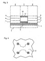
- FIG. 12 is a partial plan view of a second embodiment of a semiconductor laser device.
- a semiconductor laser device a plurality of vertical emitters 1 are arranged on a substrate 3 in a regular rectangular pattern. Pump radiation sources 2 are provided between the vertical emitters 1.
- each pump radiation source 2 can be mirrored, wherein each one or both of the end surfaces can be partially transparent and can serve as Auskoppelapt.
- Each pump radiation source 2 thus represents a laser resonator, the optical Pumps one or both adjacent vertical emitter 1 is provided.
- the semiconductor laser device of FIG. 2 acts through its plurality of vertical emitter 1 at a correspondingly small distance of the vertical emitter 1 from each other as a surface radiator. If the pump radiation sources 2 are electrically separately controllable, the semiconductor laser device can be used for display purposes.
- a multi-color representation is possible when vertical emitter 1 in different colors, for example in the three primary colors red, green, blue, are used. In such a case, an arrangement of the vertical emitter 1 in a hexagonal pattern is particularly suitable.
- Resonators for the vertical radiation can be formed by a parallel to the substrate 3, also flat and partially transparent external resonator.
- FIG. 3 is a further embodiment of a semiconductor laser device in a sectional view analogous to FIG. 1 shown.
- the same reference numerals designate the same or equivalent elements.
- FIG. 3 shows a semiconductor laser device in which an organic vertical emitter 1 is pumped by organic pump radiation sources 2.
- Both vertical emitter 1 and pump radiation sources 2 thus contain at least in the respective optical active layer, the vertical emitter zone 5 and the pumping layer 8, organic material.
- the inorganic Bragg reflector 4 it is advantageous to apply the inorganic Bragg reflector 4 in a first processing step to the substrate 3 in a planar manner.
- the pump radiation sources 2, comprising the p-side layer sequence 7, the pump radiation layer 8 and the n-side layer sequence 9, are applied.
- masking techniques are used such that areas remain free for the subsequently applied vertical emitter 1, of course, the application of pump radiation sources 2 and vertical emitter 1 can also be done in reverse order.
- the layers of the Bragg reflector 4 are usually dielectric non-conductive layers, current injection into the pump radiation sources 2 by the substrate is in contrast to the embodiment of FIG. 1 not possible in this case.
- a lateral power supply into the p-side layer sequence 7 can take place.
- This type of power supply can be advantageously used in a substrate 3 made of a non-conductive material such as glass, quartz, sapphire or plastic.
- the active vertical emitter zone 5 is applied to the Bragg reflector 4.
- the vertical emitter zone 5 contains organic semiconducting materials, preferably as a stack of layers with alternating stacked layers of an optically active and an optically inactive material.
- a waveguide layer 10 is applied and on this an internal resonator 11th
- the pump radiation layer 8 and the vertical emitter zone 5 are arranged vertically one after the other. Pump radiation generated by the pump radiation layer 8 penetrates during operation into the waveguide layer 10, in which it propagates in its lateral propagation in the vertical direction. With a suitable design of the vertical waveguide properties of the waveguide layer 10, the active vertical emitter zone 5 can be pumped laterally more homogeneously in this manner than is possible with direct lateral irradiation of the pump radiation into the vertical emitter zone 5.
- the internal resonator mirror 11 enables the operation of the semiconductor laser device even without an external resonator mirror. Due to the shorter resonator length, only a lower resonator quality can be achieved when using the internal resonator mirror 11 than when using an external resonator mirror. However, a resulting from this larger line width of the vertical radiation is irrelevant, for example, for advertising purposes.
- the internal resonator mirror 11 can be designed analogous to the Bragg reflector 4 as a dielectric mirror stack. It is particularly advantageous to form both the waveguide layer 10 and the internal resonator mirror 11 by organic layers. An application of inorganic layers to organic Layers, which is not unproblematic for thermal reasons, can be dispensed with.
- FIG. 12 is a partial plan view of a fourth embodiment of a semiconductor laser device.
- a plurality of vertical emitters 1 are arranged in a regular rectangular pattern on a substrate not visible in the figure.
- semiconductor laser device having a plurality of rod-shaped pump radiation sources 2 only one contiguous pump radiation source 2 is provided here.
- Such an arrangement can be advantageously realized with an organic pump radiation source 2, which is applied over a large area, for example by spin-coating on the substrate.
- the edges of an active layer of the pump radiation source 2 are not mirrored, so that the pump radiation source 2 is not a laser. Nevertheless, due to the large area within the active layer of the pump radiation source 2, a light intensity sufficient for optically pumping the vertical emitter 2 can be generated.
Description
Diese Patentanmeldung beansprucht die Prioritäten der deutschen Patentanmeldungen Nr.
Die Erfindung betrifft eine Halbleiterlaservorrichtung mit mindestens einem optisch gepumpten oberflächenemittierenden Vertikalemitter und mindestens einer monolithisch integrierten Pumpstrahlungsquelle zum optischen Pumpen des Vertikalemitters und ein Verfahren zu deren Herstellung.The invention relates to a semiconductor laser device having at least one optically pumped surface emitting vertical emitter and at least one monolithically integrated pump radiation source for optically pumping the vertical emitter and a method for the production thereof.
Mit optisch gepumpten vertikal emittierenden Halbleiterlaservorrichtungen lassen sich hohe Ausgangsleistungen bei gleichzeitig guter Strahlqualität verwirklichen. Durch monolithisch auf einem Substrat integrierte Pumpstrahlungsquellen kann ein kompakter Aufbau erreicht werden.With optically pumped vertically emitting semiconductor laser devices, high output powers can be achieved while maintaining good beam quality. By monolithically integrated on a substrate pump radiation sources, a compact design can be achieved.
Seitlich gepumpte anorganische Vertikalemitter und Vertikal gepumpte Vertikalemitter mit organischer aktiver Schicht sind aus
Der Erfindung liegt die Aufgabe zugrunde, eine Halbleiterlaservorrichtung der eingangs genannten Art zu schaffen, die flexibel bezüglich der Wellenlänge der von ihr erzeugten Laserstrahlung herstellbar ist. Weiterhin soll ein vorteilhaftes Verfahren zu deren Herstellung angegeben werden.The invention has for its object to provide a semiconductor laser device of the type mentioned, which is flexible with respect to the wavelength of the laser radiation generated by it produced. Furthermore, an advantageous method for their preparation should be specified.
Diese Aufgabe wird durch eine Halbleiterlaservorrichtung gemäß Patentanspruch 1 und ein Verfahren nach Patentanspruch 23 gelöst. Vorteilhafte Ausgestaltungen sind Gegenstand der jeweiligen abhängigen Ansprüche.This object is achieved by a semiconductor laser device according to
Gemäß einem ersten Aspekt der Erfindung weist die Halbleiterlaservorrichtung mindestens einen optisch gepumpten, oberflächenemittierenden Vertikalemitter mit mindestens einer strahlungserzeugenden Vertikalemitterzone auf. Weiter weist sie mindestens eine monolithisch integrierte Pumpstrahlungsquelle zum optischen Pumpen des Vertikalemitters auf, wobei die mindestens eine Pumpstrahlungsquelle zur Emission von Pumpstrahlung in einer Hauptstrahlungsrichtung eingerichtet ist, die quer zu einer Hauptstrahlungsrichtung einer Vertikalstrahlung des mindestens einen Vertikalemitters verläuft. Die Halbleiterlaservorrichtung zeichnet sich dadurch aus dass die mindestens eine Vertikalemitterzone (5) des Vertikalemitters (1) mindestens eine Schicht aufweist, die strahlungserzeugendes organisches Material enthält.According to a first aspect of the invention, the semiconductor laser device has at least one optically pumped, surface emitting vertical emitter with at least one radiation-generating vertical emitter zone. Furthermore, it has at least one monolithically integrated pump radiation source for optically pumping the vertical emitter, wherein the at least one pump radiation source is arranged to emit pump radiation in a main radiation direction that is transverse to a main radiation direction of a vertical radiation of the at least one vertical emitter. The semiconductor laser device is characterized in that the at least one vertical emitter region (5) of the vertical emitter (1) has at least one layer containing radiation-generating organic material.
Die Gruppe organischer Materialien umfasst eine Vielzahl von organischen Substanzen, die sich durch eine große Bandbreite unterschiedlicher optischer und elektrischer Eigenschaften, zum Beispiel ihrer energetischen Bandlücke, auszeichnen. Durch Auswahl geeigneter Substanzen für mindestens eine Schicht des Vertikalemitters können die optischen Eigenschaften des Vertikalemitters, zum Beispiel die Wellenlänge der Vertikalstrahlung, in weiten Grenzen gewünschten Anforderungen angepasst werden. Verglichen mit anorganischen Halbleitermaterialien lassen sich organische Materialien zudem in relativ einfachen Verfahren, zum Beispiel durch thermisches Verdampfen oder Aufschleudern in gelöster Form, auf Substrate aufbringen.The group of organic materials includes a variety of organic substances that are characterized by a wide range of different optical and electrical properties, for example their energy band gap. By selecting suitable substances for at least one layer of the vertical emitter, the optical properties of the vertical emitter, for example the wavelength of the vertical radiation, can be adjusted within wide limits to desired requirements. Compared with inorganic semiconductor materials, organic materials can also be applied to substrates in relatively simple processes, for example by thermal evaporation or spin-coating in dissolved form.
In einer vorteilhaften Ausgestaltung der Halbleiterlaservorrichtung ist das organische Material strahlungserzeugend und in der mindestens einen Vertikalemitterzone enthalten. Insbesondere auf diese Weise lassen sich die optischen Eigenschaften des Vertikalemitters in weiten Grenzen durch die Auswahl eines geeigneten organischen Materials variieren.In an advantageous embodiment of the semiconductor laser device, the organic material is radiation-generating and contained in the at least one vertical emitter zone. In particular, in this way, the optical properties of the vertical emitter can be varied within wide limits by the selection of a suitable organic material.
In einer weiteren vorteilhaften Ausgestaltung der Halbleiterlaservorrichtung ist das organische Material halbleitend. Auf diese Weise können stromführende oder ladungsträgerinjizierende Schichten als organische Schichten ausgeführt werden und mithilfe der oben genannten relativ einfachen Verfahren aufgebracht werden.In a further advantageous embodiment of the semiconductor laser device, the organic material is semiconducting. In this way, current carrying or charge carrier injecting layers can be carried out as organic layers and applied by the relatively simple procedures mentioned above.
In einer weiteren vorteilhaften Ausgestaltung der Halbleiterlaservorrichtung ist der Vertikalemitterzone in vertikaler Richtung ein interner Resonatorspiegel, insbesondere ein Bragg-Reflektor, nachgeordnet. Die Vertikalstrahlung kann dabei entweder auf einer einem Substrat gegenüberliegenden Seite ausgekoppelt werden, falls der interne Resonatorspiegel zwischen der mindestens einen Vertikalemitterzone und dem Substrat angeordnet ist und die Vertikalstrahlung, oder durch das Substrat, falls der interne Resonatorspiegel dem Substrat und der mindestens einen Vertikalemitterzone nachgeordnet ist. Im letzten Fall kann zur Auskopplung der von der mindestens einen Vertikalemitterzone erzeugten Vertikalstrahlung ein Auskoppelfenster vorgesehen ein.In a further advantageous embodiment of the semiconductor laser device, the vertical emitter zone in the vertical direction is arranged downstream of an internal resonator mirror, in particular a Bragg reflector. The vertical radiation can be coupled out either on a side opposite to a substrate if the internal resonator mirror is arranged between the at least one vertical emitter zone and the substrate and the vertical radiation or through the substrate if the internal resonator mirror is arranged downstream of the substrate and the at least one vertical emitter zone , In the latter case, a decoupling window can be provided for decoupling the vertical radiation generated by the at least one vertical emitter zone.
Gemäß weiterer vorteilhafter Ausgestaltungen der Halbleiterlaservorrichtung ist der mindestens einen Vertikalemitterzone ein externer Spiegel zugeordnet, der zusammen mit dem internen Resonatorspiegel einen Resonator für den Vertikalemitter bildet, oder es ist ein weiterer interner Resonatorspiegel vorgesehen, wobei der weitere interne Resonatorspiegel und der interne Resonatorspiegel die Vertikalemitterzone in vertikaler Richtung umschließen und so einen Resonator für die Vertikalstrahlung bilden und wobei der weitere interne Resonatorspiegel teildurchlässig ist und der Auskopplung der Vertikalstrahlung dient. Im Fall des internen Resonators kann ein kompakter Aufbau ermöglicht werden. Im Fall des externen Resonators kann eine hohe Resonatorgüte und eine entsprechend enge spektrale Breite der Vertikalstrahlung erreicht werden.According to further advantageous embodiments of the semiconductor laser device, the at least one vertical emitter zone is assigned an external mirror which together with the internal resonator mirror forms a resonator for the vertical emitter, or another internal resonator mirror is provided, wherein the further internal resonator mirror and the internal resonator mirror surround the vertical emitter zone in the vertical direction and thus form a resonator for the vertical radiation and wherein the further internal resonator mirror is partially transparent and the decoupling of the vertical radiation is used. In the case of the internal resonator, a compact structure can be made possible. In the case of the external resonator, a high resonator quality and a correspondingly narrow spectral width of the vertical radiation can be achieved.
In einer weiteren vorteilhaften Ausgestaltung der Halbleiterlaservorrichtung ist die mindestens eine Pumpstrahlungsquelle ein kantenemittierender Laser ist. Bevorzugt sind mindestens zwei Pumpstrahlungsquellen auf einander gegenüberliegenden Seiten des mindestens einen Vertikalemitters angeordnet, wobei die mindestens zwei Pumpstrahlungsquellen einen gemeinsamen Resonator aufweisen und zusammen einen Laser bilden.In a further advantageous embodiment of the semiconductor laser device, the at least one pump radiation source is an edge-emitting laser. Preferably, at least two pump radiation sources are arranged on opposite sides of the at least one vertical emitter, wherein the at least two pump radiation sources have a common resonator and together form a laser.
In weiteren vorteilhaften Ausgestaltungen der Halbleiterlaservorrichtung weist die mindestens eine Pumpstrahlungsquelle eine aktive, strahlungserzeugende Pumpschicht, die in vertikaler Richtung entweder zumindest teilweise mit der aktiven Vertikalemitterzone überlappend angeordnet ist, oder die in vertikaler Richtung der aktiven Vertikalemitterzone nachgeordnet ist.In further advantageous embodiments of the semiconductor laser device, the at least one pump radiation source has an active, radiation-generating pumping layer which is arranged either overlapping in the vertical direction at least partially with the active vertical emitter zone, or which is arranged downstream of the active vertical emitter zone.
In weiteren vorteilhaften Ausgestaltungen der Halbleiterlaservorrichtung weist die mindestens eine Pumpstrahlungsquelle eine Schichtfolge auf Basis eines III-V oder eines II-VI Verbindungshalbleiters auf oder sie weist eine Schicht auf, die ein halbleitendes organisches Material enthält. Im letzteren Fall kann das halbleitende organische Material der Pumpstrahlungsquelle ein Polymer oder eine niedermolekulare organische Verbindung sein. Ebenfalls bevorzugt ist, als halbleitendes organisches Material der mindestens einen Schicht des Vertikalemitters ein Polymer einzusetzen. Weiter ist bevorzugt, dass das halbleitende organisches Material niedermolekulare organisches Verbindungen aufweist. Polymerschichten lassen sich vorteilhaft auch großflächig, beispielsweise durch Aufschleudern in gelöster Form, einfach herstellen.In further advantageous embodiments of the semiconductor laser device, the at least one pump radiation source has a layer sequence based on a III-V or an II-VI compound semiconductor, or has a layer containing a semiconducting organic material. In the latter case, the semiconductive organic material of the pump radiation source may be a polymer or a low molecular weight organic compound. It is likewise preferred to use a polymer as the semiconducting organic material of the at least one layer of the vertical emitter. It is further preferred that the semiconductive organic material comprises low molecular weight organic compounds. Advantageously, polymer layers can also be produced over a large area, for example by spin-coating in dissolved form.
In einer weiteren vorteilhaften Ausgestaltung der Halbleiterlaservorrichtung ist die Wellenlänge der Pumpstrahlung kleiner als die Wellenlänge der Vertikalstrahlung. Auf diese Weise wird effektives optisches Pumpen ermöglicht.In a further advantageous embodiment of the semiconductor laser device, the wavelength of the pump radiation is smaller than the wavelength of the vertical radiation. In this way, effective optical pumping is enabled.
In einer weiteren vorteilhaften Ausgestaltung der Halbleiterlaservorrichtung sind mindestens zwei Vertikalemitter mit unterschiedlichen Wellenlängen ihrer Vertikalstrahlung vorgesehen. Besonders bevorzugt ist eine Mehrzahl von Vertikalemittern in einer regelmäßigen Anordnung vorgesehen. Auf diese Weise lassen sich vorteilhaft Anzeigeeinheiten und wie Flächenstrahler wirkende Einheiten realisieren.In a further advantageous embodiment of the semiconductor laser device, at least two vertical emitters with different wavelengths of their vertical radiation are provided. Particularly preferably, a plurality of vertical emitters are provided in a regular arrangement. In this way, advantageous display units and how surface radiator acting units can be realized.
Gemäß einem zweiten Aspekt der Erfindung umfasst ein Verfahren zur Herstellung einer Halbleiterlaservorrichtung der zuvor beschriebenen Art die folgenden Schritte: Es wird ein Substrat bereitgestellt, auf das eine Halbleiterschichtenfolge aufgebracht wird, wobei die Halbleiterschichtenfolge eine strahlungserzeugende Schicht aufweist und geeignet ist, eine Pumpstrahlungsquelle zu bilden. Weiter wird eine Ausnehmung in der Halbleiterschichtenfolge gebildet, in die eine Schichtenfolge aufgebracht wird, wobei die Schichtenfolge mindestens eine strahlungserzeugende Schicht aufweist und mindestens eine Schicht aufweist, die ein organisches Material enthält, und wobei die Schichtenfolge geeignet ist, einen Vertikalemitter zu bilden.According to a second aspect of the invention, a method for producing a semiconductor laser device of the type described above comprises the following steps: A substrate is provided on which a semiconductor layer sequence is applied, wherein the Semiconductor layer sequence has a radiation-generating layer and is adapted to form a pump radiation source. Furthermore, a recess is formed in the semiconductor layer sequence into which a layer sequence is applied, wherein the layer sequence has at least one radiation-generating layer and at least one layer containing an organic material, and wherein the layer sequence is suitable for forming a vertical emitter.
In einer vorteilhaften Ausgestaltung des Verfahrens zur Herstellung einer Halbleiterlaservorrichtung enthält die mindestens eine strahlungserzeugende Schicht, die in die Ausnehmung in der Halbleiterschichtenfolge aufgebracht wird, das organische Material.In an advantageous embodiment of the method for producing a semiconductor laser device, the at least one radiation-generating layer, which is applied in the recess in the semiconductor layer sequence, contains the organic material.
In weiteren vorteilhaften Ausgestaltung des Verfahrens umfasst der Schritt des Herstellen der mindestens einen Ausnehmung einen Ätzschritt oder wird durch eine Maskierung des Substrats während des Aufbringens der Halbleiterschichtenfolge realisiert.In a further advantageous embodiment of the method, the step of producing the at least one recess comprises an etching step or is realized by a masking of the substrate during the application of the semiconductor layer sequence.
Ausführungsbeispielen mit Hilfe von vier Figuren näher erläutert. Die Figuren zeigen:
Figur 1- eine schematische Schnittdarstellung eines ersten Ausführungsbeispiels einer Halbleiterlaservorrichtung,
Figur 2- eine schematische Draufsicht auf ein zweites Ausführungsbeispiel einer Halbleiterlaservorrichtung,
Figur 3- eine schematische Schnittdarstellung eines dritten Ausführungsbeispiels einer Halbleiterlaservorrichtung und
Figur 4- eine schematische Draufsicht auf ein viertes Ausführungsbeispiel einer Halbleiterlaservorrichtung.
- FIG. 1
- FIG. 2 a schematic sectional representation of a first exemplary embodiment of a semiconductor laser device, FIG.
- FIG. 2
- a schematic plan view of a second embodiment of a semiconductor laser device,
- FIG. 3
- a schematic sectional view of a third embodiment of a semiconductor laser device and
- FIG. 4
- a schematic plan view of a fourth embodiment of a semiconductor laser device.
Die Figuren sind schematische Zeichnungen. Insbesondere sind die Größenverhältnisse der Elemente und die Schichtdicken nicht maßstabsgerecht dargestellt.The figures are schematic drawings. In particular, the size ratios of the elements and the layer thicknesses are not shown to scale.
Das in
Das Ausführungsbeispiel in
Die Pumpstrahlungsquellen 2 sind in dem gezeigten Beispiel als kantenemittierende Pumplaser ausgeführt, derer laseraktives Medium die aktive Pumpschicht 8 darstellt. Die äußeren Seitenflächen der Pumpstrahlungsschicht 8 sind verspiegelt ausgeführt, sodass die beiden Pumpstrahlungsschichten 8 der Pumpstrahlungsquellen 2 zusammen mit der Vertikalemitterzone 5 gemeinsam einen Resonator für Pumpstrahlung bilden. Die Verspiegelung der Enden der Pumpstrahlungsschicht 8 kann entweder durch Aufdampfen einer hoch reflektiven Metallschicht erfolgen. An Stelle oder in Kombination mit einer Verspiegelung kann der Resonator für die Pumpstrahlung auch durch eine Strukturierung der Pumpstrahlungsschicht 8 gebildet werden, wenn durch die Strukturierung Totalreflexion an einer inneren Grenzschicht der Pumpstrahlungsschicht 8 erreicht wird. Eine solche Strukturierung besteht zum Beispiel in der Ausformung der Enden der Pumpstrahlungsschicht als prismenförmiger Retro-Reflektor.In the example shown, the
Die p-seitige Schichtenfolge 7 und die n-seitige Schichtenfolge 9 umfassen die Pumpstrahlungsschicht 8 in vertikaler Richtung und dienen sowohl der Zufuhr von Ladungsträgern, die in der Pumpstrahlungsschicht 8 strahlend rekombinieren, als auch der Wellenführung der im Betrieb entstehenden Pumpstrahlung. Um einen effektiven Pumpprozess zu ermöglichen sollte bei diesem, wie auch bei den im Folgenden gezeigten Ausführungsbeispielen die Wellenlänge der Pumpstrahlung kleiner sein als die Wellenlänge der vom Vertikalemitter 1 erzeugten Vertikalstrahlung.The p-
Die p-seitige Schichtenfolge 7 beziehungsweise die n-seitige Schichtenfolge 9 können Kontaktschichten, Mantelschichten, Wellenleiterschichten und Barriereschichten umfassen. Das Substrat 3, beispielsweise ein GaN-Substrat, ist vorteilhafterweise wie die p-seitige Schichtenfolge 7 p-dotiert. Selbstverständlich kann die Reihenfolge der p-beziehungsweise n-seitigen Schichtenfolge 7 und 9 getauscht sein und ein n-dotiertes Substrat 3 eingesetzt werden. Auf der jeweils von der aktiven Pumpstrahlungsschicht 8 abgewandten Seite der n-seitigen Schichtenfolge 9 und des Substrats 3 ist eine hier nicht gezeigte Kontaktmetallisierung zur Ladungsträgerinjektion in die Pumpstrahlungsquellen 2 vorgesehen.The p-
Im Bereich des Vertikalemitters 1 ist auf das Substrat 3 der Bragg-Reflektor 4 aufgebracht, eine Schichtenfolge, die alternierend gestapelte dielektrische Schichten mit unterschiedlichem Brechungsindex aufweist. Als Materialien kommen hier zum Beispiel TiO2 und SiO2 in Frage. Der Bragg-Reflektor 4 ist so ausgelegt, dass er für von dem Vertikalemitter 1 im Betrieb emittierte Vertikalstrahlung reflektierend ist.In the area of the
Auf dem Bragg-Reflektor 4 ist die aktive Vertikalemitterzone 5 angeordnet. Im gezeigten Beispiel umfasst die Vertikalemitterzone 5 strahlungserzeugendes organischem Material, zum Beispiel ein organisches Material mit geringem Molekulargewicht, auch niedermolekulare Verbindung oder kleinmoleküliges organisches Material genannt, ein Polymer oder eine Kombination dieser beiden Materialien.On the
Kleinmolekülige organische Materialien (small molecule material) werden typischerweise durch thermisches Verdampfen unter Vakuumbedingungen aufgebracht. Beispiele für strahlungserzeugende kleinmolekülige organische Materialien sind Tris(8-hydroxychinolinato)aluminium (Alq), 1,3-Bis(N,N-dimethylaminophenyl)-1,3,4-oxidazol (OXD-8), Oxo-bis(2-methyl-8-chinolinato)aluminium, Bis(2-methyl-8-hydroxychinolinato)aluminium; Bis(hydroxybenzochinolinato)beryllium (BeQ.sub.2), Bis(diphenylvinyl)biphenylen (DPVBI) und Arylaminsubstituiertes Distyrylarylen (DSA-Amin).Small molecule materials are typically deposited by thermal evaporation under vacuum conditions. Examples of radiation-generating small-molecule organic materials are tris (8-hydroxyquinolinato) aluminum (Alq), 1,3-bis (N, N-dimethylaminophenyl) -1,3,4-oxidazole (OXD-8), oxo-bis (2) methyl-8-quinolinato) aluminum, bis (2-methyl-8-hydroxyquinolinato) aluminum; Bis (hydroxybenzoquinolinato) beryllium (BeQ.sub.2), bis (diphenylvinyl) biphenylene (DPVBI) and arylamine-substituted distyrylarylene (DSA-amine).
Polymere werden üblicherweise durch ein Aufschleuderverfahren, auch Spincasting oder Spincoating genannt, aufgetragen. Alternativ kann auch ein räumlich selektives Abscheiden erfolgen, z.B. durch Tintenstrahldrucken. Beispiele für strahlungserzeugende Polymere sind Poly(p-phenylenvinylen) und Polyarylenvinylen sowie Copolymere von Arylen-Vinylen-Oligomeren, Polyarylene, Polychinolin sowie jeweils deren Derivate und Mischungen.Polymers are usually applied by a spin-on process, also called spin casting or spin coating. Alternatively, a spatially selective deposition can take place, for example by inkjet printing. Examples of radiation-generating polymers are poly (p-phenylenevinylene) and polyarylenevinylene and copolymers of arylene-vinylene oligomers, polyarylenes, polyquinoline and their derivatives and mixtures.
Bevorzugt ist die Vertikalemitterzone 5 nicht als eine homogene Schicht ausgestaltet, sondern als eine Schichtenfolge aus alternierend aufgebrachten optisch aktiven und optisch inaktiven Schichten. Die optisch aktiven Schichten zeichnen sich dabei durch eine hohe Quanteneffizienz für eine strahlende Rekombination von Ladungsträgerpaaren aus. Die Ladungsträgerpaare werden im Betrieb der Halbleiterlaservorrichtung durch optisches Pumpen durch die seitlich in die Vertikalemitterzone 5 eingestrahlte Pumpstrahlung der Pumpstrahlungsquellen 2 in den optisch inaktiven und/oder den optisch aktiven Schichten der Vertikalemitterzone 5 gebildet.Preferably, the
Auf die Vertikalemitterzone 5 ist die Deckschicht 6 aufgebracht, die aus einem Material besteht, das möglichst transparent für die erzeugte Vertikalemitterstrahlung ist und die typischerweise hydrophile Vertikalemitterzone 5 vor eindringender Feuchtigkeit schützt.On the
Zum Betrieb der Halbleiterlaservorrichtung ist ein in der Figur nicht gezeigter externer teildurchlässiger Resonatorspiegel vorgesehen. Der externe Resonatorspiegel bildet zusammen mit dem internen Bragg-Reflektor 4 einen Resonator für den Vertikalemitter 1.For operating the semiconductor laser device, an external partially transmissive resonator mirror, not shown in the figure, is provided. The external resonator mirror, together with the
Die in
In
Beide Seiten jeder Pumpstrahlungsquelle 2 können dabei verspiegelt sein, wobei jeweils entweder eine oder beide der Endflächen teildurchlässig sein können und als Auskoppelspiegel dienen können. Jede Pumpstrahlungsquelle 2 stellt damit einen Laserresonator dar, der zum optischen Pumpen einer oder beider benachbarter Vertikalemitter 1 vorgesehen ist.Both sides of each
Die Halbleiterlaservorrichtung der
Resonatoren für die Vertikalstrahlung können dabei durch einen parallel zum Substrat 3 angeordneten, ebenfalls flächigen und teildurchlässigen externen Resonatorspiegel gebildet werden. Alternativ ist möglich, für jeden Vertikalemitter 1 einen weiteren internen Resonatorspiegel vorzusehen, der ähnlich dem Bragg-Reflektor 4 ausgeführt sein kann.Resonators for the vertical radiation can be formed by a parallel to the
In
Das Ausführungsbeispiel in
Da die Schichten des Bragg-Reflektors 4 üblicherweise dielektrische, nicht leitende Schichten sind, ist eine Stromeinprägung in die Pumpstrahlungsquellen 2 durch das Substrat im Gegensatz zum Ausführungsbeispiel von
Im Bereich des Vertikalemitters 1 ist auf den Bragg-Reflektor 4 die aktive Vertikalemitterzone 5 aufgebracht. Wie das im Zusammenhang mit
Im Unterschied zu
Der interne Resonatorspiegel 11 ermöglicht den Betrieb der Halbleiterlaservorrichtung auch ohne externen Resonatorspiegel. Aufgrund der kürzeren Resonatorlänge kann bei Einsatz des internen Resonatorspiegels 11 nur eine geringere Resonatorgüte erreicht werden als beim Einsatz eines externen Resonatorspiegels. Eine sich daraus unter Umständen ergebende größere Linienbreite der Vertikalstrahlung ist jedoch beispielsweise für Anzeigenzwecke unerheblich. Der interne Resonatorspiegel 11 kann analog zum Bragg-Reflektor 4 als dielektrischer Spiegelstapel ausgeführt sein. Besonders vorteilhaft ist, sowohl die Wellenleiterschicht 10 als auch den internen Resonatorspiegel 11 durch organische Schichten zu bilden. Ein Aufbringen von anorganischen Schichten auf organische Schichten, das aus thermischen Gründen nicht unproblematisch ist, kann so verzichtet werden.The
In
Eine solche Anordnung kann vorteilhaft mit einer organischen Pumpstrahlungsquelle 2 realisiert werden, die großflächig beispielsweise durch Aufschleudern auf das Substrat aufgebracht wird. Die Kanten einer aktiven Schicht der Pumpstrahlungsquelle 2 werden nicht verspiegelt, sodass die Pumpstrahlungsquelle 2 kein Laser darstellt. Dennoch kann Aufgrund der großen Fläche innerhalb der aktiven Schicht der Pumpstrahlungsquelle 2 eine zum optischen Pumpen der Vertikalemitter 2 ausreichende Lichtintensität erzeugt werden.Such an arrangement can be advantageously realized with an organic
Claims (25)
- Semiconductor laser device comprising- at least one optically pumped surface emitting vertical emitter (1) having at least one radiation-generating vertical emitter zone (5),- at least one monolithically integrated pump radiation source (2) for optically pumping the vertical emitter (1) and designed for emitting pump radiation in a main radiation direction running transversely with respect to a main radiation direction of a vertical radiation of the vertical emitter (1),
characterized in that
the at least one vertical emitter zone (5) of the vertical emitter (1) has at least one layer containing radiation-generating organic material. - Semiconductor laser device according to Claim 1, characterized in that
the organic material is semiconducting. - Semiconductor laser device according to either of Claims 1 and 2, characterized in that
an internal resonator mirror is disposed downstream of the vertical emitter zone (5) in a vertical direction. - Semiconductor laser device according to Claim 3, characterized in that
the internal resonator mirror is a Bragg reflector (4). - Semiconductor laser device according to either of Claims 3 and 4, characterized in that
the internal resonator mirror is arranged between the at least one vertical emitter zone (5) and a substrate (3) and the vertical radiation is coupled out on the opposite side to the substrate (3). - Semiconductor laser device according to either of Claims 3 and 4, characterized in that
the internal resonator mirror is disposed downstream of a substrate (3) and the at least one vertical emitter zone (5) and the vertical radiation is coupled out through the substrate (3). - Semiconductor laser device according to Claim 6, characterized in that a coupling-out window is provided in the substrate for coupling out the vertical radiation generated by the at least one vertical emitter zone (5).
- Semiconductor laser device according to any of Claims 3 to 7, characterized in that
the at least one vertical emitter zone (5) is assigned an external mirror which, together with the internal resonator mirror, forms a resonator for the vertical emitter (1). - Semiconductor laser device according to any of Claims 3 to 7, characterized in that a further internal resonator mirror (11) is provided, wherein the further internal resonator mirror (11) and the internal resonator mirror enclose the vertical emitter zone (5) in a vertical direction and thus form a resonator for the vertical radiation, and wherein the further internal resonator mirror (11) is partly transmissive and serves for coupling out the vertical radiation.
- Semiconductor laser device according to any of Claims 1 to 9, characterized in that
the at least one pump radiation source (2) is an edge emitting laser. - Semiconductor laser device according to any of Claims 1 to 10, characterized in that at least two pump radiation sources (2) are arranged on mutually opposite sides of the at least one vertical emitter (1), wherein the at least two pump radiation sources (2) have a common resonator and together form a laser.
- Semiconductor laser device according to any of Claims 1 to 11, characterized in that
the at least one pump radiation source has an active, radiation-generating pump layer (8), which is arranged in a manner at least partly overlapping the active vertical emitter zone (5) in a vertical direction. - Semiconductor laser device according to any of Claims 1 to 11, characterized in that
the at least one pump radiation source (2) has an active, radiation-generating pump layer (8), which is disposed downstream of the active vertical emitter zone (5) in a vertical direction. - Semiconductor laser device according to any of Claims 1 to 13, characterized in that
the at least one pump radiation source (2) has a layer sequence based on a III-V or a II-VI compound semiconductor. - Semiconductor laser device according to any of Claims 1 to 14, characterized in that
the at least one pump radiation source (2) has at least one layer containing a semiconducting organic material. - Semiconductor laser device according to Claim 15, characterized in that
the organic material of the at least one layer of the vertical emitter (1) and/or of the pump radiation source (2) is a polymer or
in that the organic material of the at least one layer of the vertical emitter (1) and/or of the pump radiation source (2) comprises low molecular weight organic compounds. - Semiconductor laser device according to any of Claims 1 to 16, characterized in that
the wavelength of the pump radiation is less than the wavelength of the vertical radiation. - Semiconductor laser device according to any of Claims 1 to 17, characterized in that
at least two vertical emitters (1) having different wavelengths of their vertical radiation are provided. - Semiconductor laser device according to any of Claims 1 to 18, characterized in that
a plurality of vertical emitters (1) are provided in a regular arrangement. - Semiconductor laser device according to Claim 5 or 6 and according to the preceding claim, characterized in that
the plurality of vertical emitters (1) are arranged in a regular rectangular pattern on the substrate (3),
and in that the pump radiation sources (2) are provided between the vertical emitters (1). - Semiconductor laser device according to the preceding claim, characterized in that
each of the pump radiation sources (2) constitutes a laser resonator provided for optically pumping one or both adjacent vertical emitters (1). - Semiconductor laser device according to Claim 5 or 6 and according to Claim 19, characterized in that the plurality of vertical emitters (1) are arranged in a regular rectangular pattern on the substrate (3),
and in that only one continuous pump radiation source (2) is provided. - Method for producing a semiconductor laser device according to any of Claims 1 to 19, comprising the following steps:- providing a substrate (3),- applying a semiconductor layer sequence to the substrate (3), wherein the semiconductor layer sequence has a radiation-generating layer and is suitable for forming a pump radiation source (2),- producing at least one cutout in the semiconductor layer sequence,- applying a layer sequence into the at least one cutout in the semiconductor layer sequence, wherein the layer sequence has at least one radiation-generating layer containing a radiation-generating organic material, and wherein the layer sequence is suitable for forming a vertical emitter (1).
- Method according to Claim 23, wherein
the step of producing the at least one cutout comprises an etching step. - Method according to either of Claims 23 and 24, wherein
the step of producing the at least one cutout is realized by masking the substrate (3) during the process of applying the semiconductor layer sequence.
Applications Claiming Priority (2)
| Application Number | Priority Date | Filing Date | Title |
|---|---|---|---|
| DE102006045706 | 2006-09-27 | ||
| DE102007002303A DE102007002303A1 (en) | 2006-09-27 | 2007-01-16 | Semiconductor laser device, has monolithically integrated pump radiation source for optical pumping of vertical emitter and arranged for emitting pumping radiation, where emitter has layer which contains organic material |
Publications (2)
| Publication Number | Publication Date |
|---|---|
| EP1906497A1 EP1906497A1 (en) | 2008-04-02 |
| EP1906497B1 true EP1906497B1 (en) | 2011-01-05 |
Family
ID=38670004
Family Applications (1)
| Application Number | Title | Priority Date | Filing Date |
|---|---|---|---|
| EP07016842A Expired - Fee Related EP1906497B1 (en) | 2006-09-27 | 2007-08-28 | Semi-conductor laser device and method for its manufacture |
Country Status (3)
| Country | Link |
|---|---|
| US (1) | US7672353B2 (en) |
| EP (1) | EP1906497B1 (en) |
| JP (1) | JP2008085343A (en) |
Families Citing this family (4)
| Publication number | Priority date | Publication date | Assignee | Title |
|---|---|---|---|---|
| DE102007011124A1 (en) | 2007-01-25 | 2008-07-31 | Osram Opto Semiconductors Gmbh | Organic semiconductor laser and process for its production |
| EP2337168B1 (en) * | 2009-12-17 | 2019-12-25 | Forschungsverbund Berlin e.V. | Two-cavity surface-emitting laser |
| US9559734B2 (en) * | 2015-03-13 | 2017-01-31 | Qualcomm Incorporated | Robust coefficient computation for analog interference cancellation |
| WO2019216948A2 (en) | 2017-09-29 | 2019-11-14 | The Trustees Of Columbia University In The City Of New York | Compact narrow-linewidth integrated laser |
Citations (2)
| Publication number | Priority date | Publication date | Assignee | Title |
|---|---|---|---|---|
| US6876684B2 (en) * | 2001-10-12 | 2005-04-05 | Eastman Kodak Company | Organic vertical cavity lasing device having organic active region |
| EP1641092A1 (en) * | 2003-06-27 | 2006-03-29 | Semiconductor Energy Laboratory Co., Ltd. | Organic laser device |
Family Cites Families (13)
| Publication number | Priority date | Publication date | Assignee | Title |
|---|---|---|---|---|
| GB2311166A (en) * | 1996-03-13 | 1997-09-17 | Sharp Kk | An optoelectronic semiconductor device |
| US5796771A (en) * | 1996-08-19 | 1998-08-18 | The Regents Of The University Of California | Miniature self-pumped monolithically integrated solid state laser |
| US6330262B1 (en) * | 1997-05-09 | 2001-12-11 | The Trustees Of Princeton University | Organic semiconductor lasers |
| JP3515461B2 (en) * | 1999-12-28 | 2004-04-05 | 株式会社東芝 | Semiconductor light emitting device |
| DE10026734A1 (en) | 2000-05-30 | 2001-12-13 | Osram Opto Semiconductors Gmbh | Optically pumped surface emitting semiconductor laser device and method of manufacturing the same |
| DE10108079A1 (en) * | 2000-05-30 | 2002-09-12 | Osram Opto Semiconductors Gmbh | Optically-pumped surface-emitting semiconductor laser device, has edge-emitting structure of pumping source and radiation-emitting quantum pot type structure applied to common substrate |
| CA2328637A1 (en) * | 2000-12-15 | 2002-06-15 | Richard D. Clayton | Lateral optical pumping of vertical cavity surface emitting laser |
| TW595059B (en) * | 2002-05-03 | 2004-06-21 | Osram Opto Semiconductors Gmbh | Optically pumped semiconductor laser device |
| DE10223540B4 (en) * | 2002-05-27 | 2006-12-21 | Osram Opto Semiconductors Gmbh | Optically pumped semiconductor laser device |
| TWI282650B (en) * | 2002-10-11 | 2007-06-11 | Eastman Kodak Co | Organic vertical cavity lasing devices having organic active region |
| US6853660B2 (en) * | 2002-10-16 | 2005-02-08 | Eastman Kodak Company | Organic laser cavity arrays |
| US7292614B2 (en) * | 2003-09-23 | 2007-11-06 | Eastman Kodak Company | Organic laser and liquid crystal display |
| EP1683245B1 (en) | 2003-11-13 | 2011-06-15 | OSRAM Opto Semiconductors GmbH | Vcsel pumped in a monolithically optical manner and comprising a laterally applied edge emitter |
-
2007
- 2007-08-28 EP EP07016842A patent/EP1906497B1/en not_active Expired - Fee Related
- 2007-09-26 US US11/861,679 patent/US7672353B2/en not_active Expired - Fee Related
- 2007-09-27 JP JP2007251151A patent/JP2008085343A/en active Pending
Patent Citations (2)
| Publication number | Priority date | Publication date | Assignee | Title |
|---|---|---|---|---|
| US6876684B2 (en) * | 2001-10-12 | 2005-04-05 | Eastman Kodak Company | Organic vertical cavity lasing device having organic active region |
| EP1641092A1 (en) * | 2003-06-27 | 2006-03-29 | Semiconductor Energy Laboratory Co., Ltd. | Organic laser device |
Also Published As
| Publication number | Publication date |
|---|---|
| JP2008085343A (en) | 2008-04-10 |
| US7672353B2 (en) | 2010-03-02 |
| EP1906497A1 (en) | 2008-04-02 |
| US20080089379A1 (en) | 2008-04-17 |
Similar Documents
| Publication | Publication Date | Title |
|---|---|---|
| DE4135813C2 (en) | Semiconductor surface emitting laser device | |
| DE69827246T2 (en) | ORGANIC LASER | |
| EP1630915A2 (en) | Lightemitting optoelectronic element with quantum well structure and method of fabrication | |
| DE69631562T2 (en) | GaN system semiconductor laser device | |
| DE102010051286A1 (en) | Optoelectronic semiconductor chip and method for its production | |
| WO2014173820A1 (en) | Light-emitting assembly having a semiconductor layer sequence having an active zone on a columnar structure | |
| EP1906497B1 (en) | Semi-conductor laser device and method for its manufacture | |
| DE102006011284A1 (en) | Semiconductor laser device, has pumping radiation source and vertical section is configured so as to be index guiding for pumping radiation in lateral direction perpendicular to main direction of pumping radiation | |
| EP1906461B1 (en) | Method for manufacturing an optoelectronic component and optoelectronic component | |
| WO2018192972A1 (en) | Semiconductor laser diode and method for producing a semiconductor laser diode | |
| DE112016001422B4 (en) | Optoelectronic semiconductor chip | |
| DE102010047451B4 (en) | Edge-emitting semiconductor laser | |
| WO2018219667A1 (en) | Semiconductor laser diode having two resonators | |
| DE19905526C2 (en) | LED manufacturing process | |
| EP3918679A1 (en) | Device for generating a laser beam | |
| DE60116827T2 (en) | InGaAsP semiconductor laser | |
| WO2010048918A1 (en) | Optoelectronic semiconductor chip and method for producing an optoelectronic semiconductor chip | |
| DE102007002303A1 (en) | Semiconductor laser device, has monolithically integrated pump radiation source for optical pumping of vertical emitter and arranged for emitting pumping radiation, where emitter has layer which contains organic material | |
| DE102013211707B4 (en) | Single support array, multiple array array and method of making an array | |
| DE19840436A1 (en) | LED, especially a powerful red to yellowish green emitting aluminum gallium indium phosphide LED, has upper cladding structure including thin high ohmic layer | |
| EP0663110B1 (en) | Semiconductor laser with an active film disposed between two resonator mirrors, and a method for producing the laser | |
| WO2022122347A1 (en) | Semiconductor laser and method for producing a semiconductor laser | |
| WO2023143918A1 (en) | Laser diode component, and method for producing at least one photonic crystal structure for a laser diode component | |
| DE102021129563A1 (en) | COMPONENT WITH INTEGRATED CONVERTER LAYER AND METHOD FOR MANUFACTURING A COMPONENT | |
| DE102021100391A1 (en) | EDGE EMITTING SEMICONDUCTOR LASER DIODE AND METHOD FOR MANUFACTURING AN EDGE EMITTING SEMICONDUCTOR LASER DIODE |
Legal Events
| Date | Code | Title | Description |
|---|---|---|---|
| PUAI | Public reference made under article 153(3) epc to a published international application that has entered the european phase |
Free format text: ORIGINAL CODE: 0009012 |
|
| AK | Designated contracting states |
Kind code of ref document: A1 Designated state(s): AT BE BG CH CY CZ DE DK EE ES FI FR GB GR HU IE IS IT LI LT LU LV MC MT NL PL PT RO SE SI SK TR |
|
| AX | Request for extension of the european patent |
Extension state: AL BA HR MK YU |
|
| 17P | Request for examination filed |
Effective date: 20080821 |
|
| 17Q | First examination report despatched |
Effective date: 20080925 |
|
| AKX | Designation fees paid |
Designated state(s): DE |
|
| GRAP | Despatch of communication of intention to grant a patent |
Free format text: ORIGINAL CODE: EPIDOSNIGR1 |
|
| GRAS | Grant fee paid |
Free format text: ORIGINAL CODE: EPIDOSNIGR3 |
|
| GRAA | (expected) grant |
Free format text: ORIGINAL CODE: 0009210 |
|
| AK | Designated contracting states |
Kind code of ref document: B1 Designated state(s): DE |
|
| REF | Corresponds to: |
Ref document number: 502007006163 Country of ref document: DE Date of ref document: 20110217 Kind code of ref document: P |
|
| REG | Reference to a national code |
Ref country code: DE Ref legal event code: R096 Ref document number: 502007006163 Country of ref document: DE Effective date: 20110217 |
|
| PLBE | No opposition filed within time limit |
Free format text: ORIGINAL CODE: 0009261 |
|
| STAA | Information on the status of an ep patent application or granted ep patent |
Free format text: STATUS: NO OPPOSITION FILED WITHIN TIME LIMIT |
|
| 26N | No opposition filed |
Effective date: 20111006 |
|
| REG | Reference to a national code |
Ref country code: DE Ref legal event code: R097 Ref document number: 502007006163 Country of ref document: DE Effective date: 20111006 |
|
| PGFP | Annual fee paid to national office [announced via postgrant information from national office to epo] |
Ref country code: DE Payment date: 20180823 Year of fee payment: 12 |
|
| REG | Reference to a national code |
Ref country code: DE Ref legal event code: R119 Ref document number: 502007006163 Country of ref document: DE |
|
| PG25 | Lapsed in a contracting state [announced via postgrant information from national office to epo] |
Ref country code: DE Free format text: LAPSE BECAUSE OF NON-PAYMENT OF DUE FEES Effective date: 20200303 |