JP5201886B2 - Electrophotographic equipment - Google Patents
Electrophotographic equipment Download PDFInfo
- Publication number
- JP5201886B2 JP5201886B2 JP2007162431A JP2007162431A JP5201886B2 JP 5201886 B2 JP5201886 B2 JP 5201886B2 JP 2007162431 A JP2007162431 A JP 2007162431A JP 2007162431 A JP2007162431 A JP 2007162431A JP 5201886 B2 JP5201886 B2 JP 5201886B2
- Authority
- JP
- Japan
- Prior art keywords
- charging roller
- charging
- conductive layer
- carbon black
- layer
- Prior art date
- Legal status (The legal status is an assumption and is not a legal conclusion. Google has not performed a legal analysis and makes no representation as to the accuracy of the status listed.)
- Active
Links
Images


Landscapes
- Photoreceptors In Electrophotography (AREA)
- Electrostatic Charge, Transfer And Separation In Electrography (AREA)
- Rolls And Other Rotary Bodies (AREA)
Description
本発明は、主にレーザープリンター、複写機等の電子写真装置に用いられる帯電ローラ及び、該帯電ローラを有する電子写真装置に関する。 The present invention relates to a charging roller mainly used in an electrophotographic apparatus such as a laser printer and a copying machine, and an electrophotographic apparatus having the charging roller.
従来、電子写真装置内部には画像形成部が設置されており、記録画像はクリーニング、帯電、潜像、現像、転写、定着プロセスを経て形成される。画像形成部は、電子写真感光体である感光ドラムを備えており、クリーニング部、帯電部、潜像形成部、現像部及び転写部を備えている。この画像形成部で形成された感光ドラム上の画像は転写部で記録材に転写され、定着部に搬送された後に定着部にて加熱及び加圧され、記録材に定着された記録画像として出力される。 Conventionally, an image forming unit is installed inside an electrophotographic apparatus, and a recorded image is formed through processes of cleaning, charging, latent image, development, transfer, and fixing. The image forming unit includes a photosensitive drum that is an electrophotographic photosensitive member, and includes a cleaning unit, a charging unit, a latent image forming unit, a developing unit, and a transfer unit. The image on the photosensitive drum formed by the image forming unit is transferred to a recording material by a transfer unit, conveyed to the fixing unit, heated and pressed by the fixing unit, and output as a recording image fixed on the recording material. Is done.
次に、帯電、潜像形成、現像、転写プロセスについて説明する。 Next, charging, latent image formation, development, and transfer processes will be described.
帯電部では、帯電ローラにより感光体の表面に、所定の極性で、電位が一様になるように一次帯電を行う。次に、目的画像情報の露光を受けることで、感光体表面に目的画像に対応した静電潜像が形成される。この静電潜像は、現像部にて現像部材よりトナー画像として可視化される。可視化されたトナー画像は、転写部において転写部材よって感光体表面から記録材に転写される。転写された未定着のトナー画像は、定着部に搬送されて、定着部で定着されて記録画像として出力される。 In the charging unit, the charging roller performs primary charging on the surface of the photoconductor so that the potential is uniform with a predetermined polarity. Next, by receiving exposure of target image information, an electrostatic latent image corresponding to the target image is formed on the surface of the photoreceptor. This electrostatic latent image is visualized as a toner image from the developing member in the developing unit. The visualized toner image is transferred from the surface of the photosensitive member to the recording material by the transfer member at the transfer portion. The transferred unfixed toner image is conveyed to a fixing unit, fixed by the fixing unit, and output as a recorded image.
電子写真装置や静電記録装置などの画像形成装置に用いられる帯電方式として、コロナ帯電方式とローラ帯電方式がある。コロナ帯電方式はコロナワイヤーなどに電圧を印加して、帯電生成物を形成し、感光体表面を帯電生成物によって帯電させる帯電方法である。一方、ローラ帯電方式は、帯電ローラを感光体に接触もしくは近接(帯電ローラと感光体間距離が数十μm)させて、感光体表面を放電によって帯電させる帯電方法である。 There are a corona charging method and a roller charging method as charging methods used in image forming apparatuses such as electrophotographic apparatuses and electrostatic recording apparatuses. The corona charging method is a charging method in which a voltage is applied to a corona wire or the like to form a charged product, and the surface of the photoreceptor is charged with the charged product. On the other hand, the roller charging method is a charging method in which the surface of the photosensitive member is charged by discharging by bringing the charging roller into contact with or close to the photosensitive member (the distance between the charging roller and the photosensitive member is several tens of μm).
ローラ帯電方式は、コロナ帯電方式に比べて発生するオゾンや放電生成物の量が圧倒的に少ない。よって、ローラ帯電方式を用いることで、オゾンフィルターをつけるスペースを削減することや、放電生成物による画像ボケ等を軽減させることが可能である。 The roller charging method has an extremely small amount of ozone and discharge products generated compared to the corona charging method. Therefore, by using the roller charging method, it is possible to reduce the space for attaching the ozone filter and to reduce image blur due to the discharge product.
ローラ帯電方式は、直流電流(DC)に交流電流(AC)を重畳したAC+DC帯電と、DCのみのDC帯電に分別される。DC帯電は小型化、ローコストを達成するには好適な技術であるが、感光体のドラム電位を一定にする帯電バイアス域が狭く、ローラ抵抗の周ムラや汚れによる微小な抵抗ムラ、ローラの不均一性による帯電不均一性など、画質安定性を達成するのが技術的に難しい。これが印刷速度50枚機以上、メンテナンス間隔が25万枚以上の高速長寿命なオフィス用複写機になると、DC帯電方式では画質の維持がさらに困難となるため、AC+DC帯電方式が好適である。 The roller charging method is classified into AC + DC charging in which alternating current (AC) is superimposed on direct current (DC), and DC charging only in DC. DC charging is a suitable technique for achieving downsizing and low cost, but the charging bias region for keeping the drum potential of the photoconductor constant is narrow, and the roller resistance is uneven due to circumferential unevenness and dirt, and roller non-uniformity. It is technically difficult to achieve image quality stability such as non-uniform charging due to uniformity. If this is a high-speed and long-life office copying machine with a printing speed of 50 sheets or more and a maintenance interval of 250,000 sheets or more, it is more difficult to maintain image quality with the DC charging system, so the AC + DC charging system is suitable.
しかし、AC+DC帯電方式によるローラ帯電における課題としては、帯電ローラの通電劣化が挙げられる。通電劣化とは、帯電ローラに電流を流すことにより、ローラ抵抗が変化してしまうことをいう。ローラ抵抗が変化してしまうと、帯電ローラが感光体に所望のドラム電位を与えることができなくなる。一般的には、通電劣化が生じるとローラ抵抗は上昇してしまうため、ドラム電位が低下してしまうことになる。通電劣化を解決するための検討として、特許文献1〜3に関連技術が報告されている。
However, a problem in roller charging by the AC + DC charging system is deterioration of energization of the charging roller. The deterioration of energization means that the roller resistance is changed by passing a current through the charging roller. If the roller resistance changes, the charging roller cannot give a desired drum potential to the photoreceptor. In general, when energization deterioration occurs, the roller resistance increases, so that the drum potential decreases. Related art has been reported in
近年、電子写真装置には高画質、長寿命化が要求されつつある。 In recent years, an electrophotographic apparatus is required to have high image quality and a long life.
高画質化を満たすための電子写真感光体からのアプローチとしては、例えば以下の2つを挙げることができる。(1)電子写真感光体の薄膜化により電子写真感光体の静電容量を増加させて潜像のコントラストをより鮮明にする方法。(2)短波長のレーザー(特に380〜500nm)対応の電子写真感光体を採用する方法。 As an approach from the electrophotographic photosensitive member to satisfy the high image quality, for example, the following two can be mentioned. (1) A method of increasing the electrostatic capacitance of the electrophotographic photosensitive member by thinning the electrophotographic photosensitive member to make the contrast of the latent image clearer. (2) A method of employing an electrophotographic photosensitive member corresponding to a short wavelength laser (particularly 380 to 500 nm).
また、長寿命化を満たすための電子写真感光体からのアプローチとしては、例えば以下の2つの方法が挙げられる。(1)珪素原子を母体とする非結晶材料で構成された感光体、例えばアモルファスシリコン感光体を用いる方法。(2)感光層を保護する表面保護層を設ける方法。
しかし、アモルファスシリコン感光体や薄膜有機感光体を使用した電子写真プロセスにおいてローラ帯電方式を採用すると、感光体の静電容量が大きいため、帯電するのに大電流が必要となる。帯電ローラに大電流が流れると、帯電ローラの高抵抗化(通電劣化)が進行しやすくなり、長寿命化が達成できない。したがって、帯電ローラの大電流通電条件(例えば、直流電流0.2mA以上かつ交流電流2mA以上)における通電劣化対策が重要な課題となっている。 However, when a roller charging method is employed in an electrophotographic process using an amorphous silicon photoreceptor or a thin film organic photoreceptor, a large current is required for charging because the electrostatic capacity of the photoreceptor is large. When a large current flows through the charging roller, the charging roller tends to increase in resistance (energization deterioration), and a long life cannot be achieved. Therefore, countermeasures against energization deterioration in a large current energizing condition of the charging roller (for example, a DC current of 0.2 mA or more and an AC current of 2 mA or more) are an important issue.
特許文献1〜3には、通電前後の抵抗変化が小さい帯電ローラに関する発明が記載されているが、これらの特許文献に記載される通電条件は低電流であるため、本発明の課題を解決する手段にはならない。
したがって、本発明は、大電流を通電しても通電劣化が生じない帯電ローラを提供することを目的とする。 Accordingly, an object of the present invention is to provide a charging roller in which energization deterioration does not occur even when a large current is applied.
本発明者らは上記課題を解決すべく鋭意検討したところ、通電劣化が生じる原因は、大電流を流したときに発生するジュール熱によって導電層を形成するベースポリマーや導電性粒子等の分子運動が活性化され、この分子運動によって導電層中における導電性粒子の分散状態が変化するためであることを発見した。そこで、分子運動の指標である水素核スピン−スピン緩和時間T2を特定の範囲とすることで、通電劣化を抑制できることが判明した。 The inventors of the present invention diligently studied to solve the above-mentioned problems, and the cause of the deterioration of energization is the molecular motion of the base polymer and conductive particles that form the conductive layer by Joule heat generated when a large current is passed. It was discovered that the dispersion state of the conductive particles in the conductive layer is changed by this molecular motion. Thus, it has been found that the deterioration of energization can be suppressed by setting the hydrogen nucleus spin-spin relaxation time T 2 that is an index of molecular motion within a specific range.
すなわち、本発明に係る帯電ローラは、導電性支持体の上に導電性粒子を含有する導電層を有する帯電ローラであって、該導電層の23℃における水素核スピン−スピン緩和時間T2が20μs<T2<300μsであることを特徴とする。 That is, the charging roller according to the present invention is a charging roller having a conductive layer containing conductive particles on a conductive support, and the hydrogen nucleus spin-spin relaxation time T 2 of the conductive layer at 23 ° C. 20 μs <T 2 <300 μs.
また、本発明に係る電子写真装置は、前記帯電ローラを具備することを特徴とする。 In addition, an electrophotographic apparatus according to the present invention includes the charging roller.
本発明に係る帯電ローラは、大電流を流してもローラ抵抗が変化せず、通電劣化を生じない。したがって本発明に係る帯電ローラは、大電流通電条件が必要なアモルファスシリコン感光体や薄膜有機感光体等を搭載する電子写真装置において、通電劣化という問題を生ずることなく使用可能である。 In the charging roller according to the present invention, even when a large current is passed, the roller resistance does not change, and energization deterioration does not occur. Therefore, the charging roller according to the present invention can be used in an electrophotographic apparatus equipped with an amorphous silicon photoconductor or a thin film organic photoconductor that requires a large current energization condition without causing a problem of energization deterioration.
本発明者らは鋭意検討したところ、以下に述べるように、大電流通電条件における通電劣化を解決する手段として、導電性粒子を含有し低分子運動性の導電層を有する帯電ローラが必須であることが明らかになった。 As a result of intensive studies, the present inventors have found that a charging roller containing conductive particles and having a low molecular mobility conductive layer is indispensable as a means for solving the deterioration in energization under large current energization conditions. It became clear.
通電劣化メカニズムを検討した結果、大電流通電条件における通電劣化の原因は、導電性粒子の分散状態の変化にあることが判明した。すなわち、大電流を帯電ローラに通電することにより発生するジュール熱によって導電層を形成するベースポリマー(高分子、ゴム等)の分子運動が活性化され、この分子運動によって導電層中に分散する導電性粒子の分散状態が通電前後において変化する。そのために、ローラ抵抗が変化してしまうことが判った。このメカニズムから、通電劣化を抑制する材料的対策として、以下の二つが非常に効果的であることが判明した。
(1)低分子運動性の材料からなる導電層とすること。
(2)導電性粒子としては分子の熱運動の影響を受け難い比較的大きな粒径のものを使用すること。
As a result of studying the energization deterioration mechanism, it has been found that the cause of the energization deterioration under a large current energization condition is a change in the dispersion state of the conductive particles. That is, the molecular motion of the base polymer (polymer, rubber, etc.) that forms the conductive layer is activated by Joule heat generated by passing a large current through the charging roller, and this molecular motion disperses in the conductive layer. The dispersion state of the conductive particles changes before and after energization. For this reason, it has been found that the roller resistance changes. From this mechanism, it has been found that the following two are very effective as material countermeasures for suppressing current deterioration.
(1) A conductive layer made of a low molecular mobility material.
(2) Use conductive particles having a relatively large particle size that are hardly affected by thermal motion of molecules.
まず(1)の条件について検討した。 First, the condition (1) was examined.
ここで、低分子運動性の材料とは、熱運動の小さい分子からなる材料(高分子、樹脂またはゴム)を意味する。なお、導電層の抵抗値としては、例えば104Ω〜107Ωを選択することができる。 Here, the low molecular mobility material means a material (polymer, resin or rubber) composed of molecules having small thermal motion. In addition, as a resistance value of the conductive layer, for example, 10 4 Ω to 10 7 Ω can be selected.
ここで、分子運動性はパルスNMRの水素核スピン−スピン緩和時間(T2)によってあらわすことができる。これはプロトンの核磁気共鳴法で分析して得られるFID(Free Induction Decay:自由誘導減衰)強度曲線あるいはエコー強度の減衰曲線から得られる水素核スピン−スピン緩和時間(T2)の平均値である。導電層のT2を測定すると、ベースポリマーに由来するT2成分だけでなく、導電層中に含有される成分(カーボンブラック等の添加剤)に由来するT2成分も観測される。それら観測された成分を平均したものを導電層のT2として分子運動性の指標として用いた。T2が小さいと導電層の分子運動性が小さく、T2が大きいと分子運動性が大きいことを示す。 Here, the molecular mobility can be expressed by the hydrogen nuclear spin-spin relaxation time (T 2 ) of pulse NMR. This is the average value of the hydrogen nuclear spin-spin relaxation time (T 2 ) obtained from the FID (Free Induction Decay) intensity curve or the echo intensity attenuation curve obtained by analysis by proton nuclear magnetic resonance. is there. When measuring the T 2 of the conductive layer, not only T 2 components derived from the base polymer, T 2 components derived from components (additives such as carbon black) contained in the conductive layer is also observed. An average of these observed components was used as an index of molecular mobility as T 2 of the conductive layer. When T 2 is small, the molecular mobility of the conductive layer is small, and when T 2 is large, the molecular mobility is large.
そこで、本発明者らは分子運動性を示すT2と導電層の関係について検討したところ、導電層のT2が所定の範囲にある場合、大電流を流しても、ローラ抵抗値の変化がなく、通電劣化が生じないことを見出した。 Therefore, the present inventors examined the relationship between T 2 exhibiting molecular mobility and the conductive layer. As a result, when T 2 of the conductive layer is within a predetermined range, the roller resistance value does not change even when a large current is passed. It was found that there was no deterioration of energization.
したがって、本発明に係る帯電ローラは、導電性支持体上に導電性粒子を含有する導電層を有する帯電ローラであって、該導電層の23℃における水素核スピン−スピン緩和時間T2が20μs<T2<300μsであることを特徴とする帯電ローラである。 Therefore, the charging roller according to the present invention is a charging roller having a conductive layer containing conductive particles on a conductive support, and the hydrogen nucleus spin-spin relaxation time T 2 at 23 ° C. of the conductive layer is 20 μs. The charging roller is characterized in that <T 2 <300 μs.
前記導電層は、23℃におけるT2(μs)が20超300未満の範囲にあることを特徴とする。20以下では、導電層が硬くなりすぎて、帯電ローラとして適さない。また、T2が300以上では、導電層に大電流が流れた時に生じるジュール熱で起こる分子の動きにより、導電層内部に存在する導電性粒子の分散状態が変化してしまう。このような導電性粒子の分散状態の変化が大電流通電条件における通電劣化の原因である。すなわち、23℃におけるT2(μs)が20超300未満である導電層は、大電流が流れても導電性粒子の分散状態を維持でき、大電流通電によりローラ抵抗が変化しにくい。 The conductive layer is characterized in that T 2 (μs) at 23 ° C. is in the range of more than 20 and less than 300. If it is 20 or less, the conductive layer becomes too hard and it is not suitable as a charging roller. On the other hand, when T 2 is 300 or more, the dispersion state of the conductive particles existing inside the conductive layer changes due to the movement of molecules caused by Joule heat generated when a large current flows through the conductive layer. Such a change in the dispersion state of the conductive particles is a cause of deterioration of energization under a large current energization condition. That is, the conductive layer having T 2 (μs) at 23 ° C. of more than 20 and less than 300 can maintain the dispersed state of the conductive particles even when a large current flows, and the roller resistance hardly changes due to the large current flow.
なお、T2(μs)の測定温度に関しては、温度が変化するとT2(μs)の値も変化するため、23℃と規定した。この温度は標準的な室温であり、この温度において帯電ローラ、帯電ローラを搭載したカートリッジ又は電子写真装置が最も使用されると考えられる。また、T2(μs)の大小関係は、別の温度でも変わらないことを確認している。 Regarding the measured temperature of T 2 (.mu.s), since the varying value of the temperature changes T 2 (.mu.s), it was defined as 23 ° C.. This temperature is a standard room temperature, and it is considered that a charging roller, a cartridge equipped with a charging roller, or an electrophotographic apparatus is most used at this temperature. It has also been confirmed that the magnitude relationship of T 2 (μs) does not change even at different temperatures.
前記導電層を構成するベースポリマーとしては、23℃における導電層のT2(μs)が20超300未満の範囲とすることができる材料であれば特に限定されない。通常、ブタジエンゴム、スチレンゴム、エチレンプロピレンゴム、アクリロニトリル−ブタジエンゴム、エピクロルヒドリン系ゴム等を使用することが可能である。これらのうち、本発明では、特にアクリロニトリル含有率が25%超49%未満のアクリルニトリル−ブタジエンゴム(以下、NBRと略す)が好ましく挙げられる。ニトリル基は分子運動性を下げる効果があり、NBR中のアクリロニトリル含有率が増えると、導電層のT2(μs)が下がる。この現象について確認したところ、NBR中のアクリロニトリル含有率が49%以上になると、導電層のT2(μs)が20以下になってしまう場合があり、導電層が硬くなりやすい。導電層が硬くなると、加硫時、研磨時又はUV処理等の工程において導電層に亀裂等の不良が発生しやすくなる。亀裂が発生する原因は不明であるが、導電層が硬くなりすぎると、外部応力や導電層の収縮等の内部応力によって、導電層にひび割れが入ってしまうものと考えられる。一方、NBRのアクリロニトリル含有率が25%以下であると、T2(μs)が300以上になってしまい、導電層に大電流が流れた時に起こる分子の動きにより、導電層内部に存在する導電性粒子の分散状態が変化してしまう。なお、NBR中のアクリロニトリル含有率(%)とは、アクリロニトリルとブタジエンを重合してNBRを合成する場合におけるアクリロニトリルの質量%を指す。例えば、アクリロニトリルの含有率が25%のNBRとは、アクリロニトリル25質量%とブタジエン75質量%を重合したものをいう。 The base polymer constituting the conductive layer is not particularly limited as long as the T 2 (μs) of the conductive layer at 23 ° C. can be in the range of more than 20 and less than 300. Usually, butadiene rubber, styrene rubber, ethylene propylene rubber, acrylonitrile-butadiene rubber, epichlorohydrin rubber, or the like can be used. Of these, acrylonitrile-butadiene rubber (hereinafter abbreviated as NBR) having an acrylonitrile content of more than 25% and less than 49% is particularly preferred in the present invention. A nitrile group has an effect of lowering molecular mobility, and when the acrylonitrile content in NBR increases, T 2 (μs) of the conductive layer decreases. When this phenomenon was confirmed, when the acrylonitrile content in NBR is 49% or more, T 2 (μs) of the conductive layer may be 20 or less, and the conductive layer tends to be hard. When the conductive layer becomes hard, defects such as cracks are likely to occur in the conductive layer during vulcanization, polishing or UV treatment. The cause of the occurrence of cracks is unknown, but if the conductive layer becomes too hard, it is considered that the conductive layer cracks due to internal stress such as external stress or contraction of the conductive layer. On the other hand, when the acrylonitrile content of NBR is 25% or less, T 2 (μs) becomes 300 or more, and the electric conductivity existing inside the conductive layer is caused by the movement of molecules that occurs when a large current flows through the conductive layer. The dispersion state of the conductive particles changes. In addition, the acrylonitrile content rate (%) in NBR refers to the mass% of acrylonitrile in the case of synthesizing NBR by polymerizing acrylonitrile and butadiene. For example, NBR having an acrylonitrile content of 25% refers to a polymer of 25% by mass of acrylonitrile and 75% by mass of butadiene.
次に、上記(2)の条件について検討した。 Next, the condition (2) was examined.
導電性粒子は、本発明の導電層が好適な導電性を発現するために用いられるもので、特に限定されるものではない。例えば、カーボンブラック、黒鉛、炭素繊維等の炭素材料、アルミニウム、マグネシウム等の金属粉、金属繊維等の金属材料、表面処理された金属酸化物粉等が挙げられる。これらのうち、材料コストや分散性を考慮すると、カーボンブラックが特に好ましい。カーボンブラックとして、材料コストや分散性の観点から、MTカーボンが特に好ましい。また、本発明では、異なる種類の導電性粒子を併用することができる。 The conductive particles are used for the conductive layer of the present invention to exhibit suitable conductivity, and are not particularly limited. Examples thereof include carbon materials such as carbon black, graphite and carbon fibers, metal powders such as aluminum and magnesium, metal materials such as metal fibers, and surface-treated metal oxide powders. Among these, carbon black is particularly preferable in consideration of material cost and dispersibility. As carbon black, MT carbon is particularly preferable from the viewpoint of material cost and dispersibility. Moreover, in this invention, a different kind of electroconductive particle can be used together.
前記導電性粒子の平均粒径(電子顕微鏡による算術平均粒子径)(以下、平均粒径と略す)は、特に制限されるものではないが、通電劣化を防止するという観点から、75nm超300nm未満であることが好ましく、80nm以上230nm以下であることがより好ましい。比較的大きい粒径の導電性粒子は、ベースポリマーの分子運動の影響によって分散状態が変化し難い。そのため、比較的大きい平均粒径(75nm超)の導電性粒子を導電性付与剤として用いることで、大電流通電条件での導電層の分子運動で起こる導電性粒子の分散状態の変化を抑制することができ、帯電ローラの通電劣化を防止することができる。一方、平均粒径が75nm以下の導電性粒子の場合、ベースポリマーの分子運動の影響を受けやすく、分散状態の変化によって導電性の高い粒子による導電パスを補強する効果が低減する可能性がある。さらに、平均粒径が300nm以上の導電性粒子の場合、導電層の表面近傍にこのような大粒径の導電性粒子が存在すると、感光体ドラムの微小な傷に対してリークしやすくなるという弊害が生じる場合がある。したがって、平均粒径が75nm超300nm未満の導電性粒子は、分散状態の変化を起こしにくく、導電パスを補強する効果を示し、かつ、感光体ドラムリークを起こしくいため、導電性を付与する材料として好適である。 The average particle diameter (arithmetic average particle diameter by electron microscope) (hereinafter abbreviated as average particle diameter) of the conductive particles is not particularly limited, but from the viewpoint of preventing energization deterioration, more than 75 nm and less than 300 nm. It is preferable that it is 80 nm or more and 230 nm or less. The conductive particles having a relatively large particle diameter are unlikely to change in dispersion state due to the molecular motion of the base polymer. Therefore, by using conductive particles having a relatively large average particle size (over 75 nm) as a conductivity-imparting agent, it is possible to suppress a change in the dispersion state of the conductive particles caused by molecular motion of the conductive layer under a large current conduction condition. It is possible to prevent the electrification deterioration of the charging roller. On the other hand, in the case of conductive particles having an average particle size of 75 nm or less, it is easily affected by the molecular motion of the base polymer, and there is a possibility that the effect of reinforcing the conductive path by the highly conductive particles due to the change in the dispersion state may be reduced. . Furthermore, in the case of conductive particles having an average particle size of 300 nm or more, if such large particle size conductive particles exist in the vicinity of the surface of the conductive layer, it is easy to leak against minute scratches on the photosensitive drum. Detrimental effects may occur. Therefore, the conductive particles having an average particle diameter of more than 75 nm and less than 300 nm are less likely to cause a change in dispersion state, exhibit an effect of reinforcing the conductive path, and are less likely to cause a photoconductor drum leak. It is suitable as.
前記導電性粒子の配合量としては、ベースポリマー100質量部に対して、20質量部以上100質量部以下が好ましく、40質量部以上60質量部以下がより好ましい。20質量部未満では導電パスを補強する効果が低減する場合がある。100質量部超では、導電パスを補強する効果は得られるが、導電層が硬くなりすぎて亀裂発生等の不良が発生しやすくなる場合がある。 As a compounding quantity of the said electroconductive particle, 20 mass parts or more and 100 mass parts or less are preferable with respect to 100 mass parts of base polymers, and 40 mass parts or more and 60 mass parts or less are more preferable. If it is less than 20 parts by mass, the effect of reinforcing the conductive path may be reduced. If it exceeds 100 parts by mass, the effect of reinforcing the conductive path can be obtained, but the conductive layer may become too hard and defects such as cracking may easily occur.
また、導電性粒子としては導電性の高いものが好ましく、特に好適に使用されるカーボンブラックとしては、例えば、窒素吸着比表面積(N2SA)やDBP(ジブチルフタレイト)吸油量の大きなカーボンブラック等が挙げられる。さらに、平均粒径が75nm超300nm未満の粒径を有するカーボンブラックとしては、例えば、MTカーボンやFTカーボンが挙げられる。 Further, the conductive particles are preferably those having high conductivity, and particularly suitably used carbon blacks include, for example, carbon black having a large nitrogen adsorption specific surface area (N 2 SA) and DBP (dibutyl phthalate) oil absorption. Etc. Furthermore, examples of carbon black having an average particle size of more than 75 nm and less than 300 nm include MT carbon and FT carbon.
また、本発明の帯電ローラには、上記のベースポリマー、導電性粒子の他に、充填剤、可塑剤、加硫剤、加硫促進剤、老化防止剤等を、任意に添加することができる。 In addition to the above base polymer and conductive particles, a filler, a plasticizer, a vulcanizing agent, a vulcanization accelerator, an antiaging agent, and the like can be arbitrarily added to the charging roller of the present invention. .
本発明の帯電ローラの製造方法について説明する。 A method for manufacturing the charging roller of the present invention will be described.
帯電ローラの製造工程は、混練工程、成形工程及び研磨工程に分けられる。 The charging roller manufacturing process is divided into a kneading process, a molding process, and a polishing process.
混練工程では、例えば、前記ベースポリマー、前記導電性粒子、加硫助剤、可塑剤、充填剤等を加圧ニーダーで混練し、その後、ロール混練機で加硫剤、加硫促進剤等を混練する。 In the kneading step, for example, the base polymer, the conductive particles, the vulcanization aid, the plasticizer, the filler, and the like are kneaded with a pressure kneader, and then the vulcanizer, the vulcanization accelerator, and the like are mixed with a roll kneader. Knead.
成形工程では、混錬工程で製造された混合物を一軸スクリュー押出し機でロール状に押出し、加硫缶で加硫し、接着剤を塗布した導電性支持体(芯金)に圧入する。または、押出物を芯金に直接コートし、熱風炉で加硫することもできる。ここで、導電層の熱処理は、140℃〜170℃、50分〜130分が好ましい。 In the molding process, the mixture produced in the kneading process is extruded into a roll with a single screw extruder, vulcanized with a vulcanizing can, and press-fitted into a conductive support (core metal) coated with an adhesive. Alternatively, the extrudate can be directly coated on the core and vulcanized in a hot air furnace. Here, the heat treatment of the conductive layer is preferably 140 to 170 ° C. and 50 to 130 minutes.
研磨工程では、成形工程で得られた未研磨の導電層の表面を研磨し、本発明に係る帯電ローラを製造する。研磨方法としては、以下の方法を挙げることができる。(1)帯電ローラの長さ(長手幅)と同サイズの砥石を用いて長手方向を一度に研磨する方法。(2)薄型の砥石を長手方向にトラバースさせながら研磨する方法。 In the polishing step, the surface of the unpolished conductive layer obtained in the molding step is polished to manufacture the charging roller according to the present invention. Examples of the polishing method include the following methods. (1) A method of polishing the longitudinal direction at once using a grindstone having the same size as the length (longitudinal width) of the charging roller. (2) A method of polishing while traversing a thin grindstone in the longitudinal direction.
本発明の帯電ローラは、発明の効果を損なわない範囲で、表面層を設けることができる。例えば、紫外光や電子線で硬化する樹脂を表面に塗布し光硬化させることで、表面の摩擦係数や撥水性、撥油性等を制御することができ、帯電ローラを汚染から防ぐことができる。また、紫外光照射、電子線照射等により表面改質を行うことも可能である。ここで、紫外光照射による表面処理(UV処理)としては、例えば、200〜450nmの波長の光を導電層表面に均一に照射することができる。UV処理時間は1〜30分程度行えばよい。紫外光照射は導電層表面に均一に照射させることが好ましく、例えば、紫外光の光源に対して導電層を回転させるか、導電層をコンベアーで送りながら上下方向から紫外光を照射するなどの方法を用いることができる。この時、UV処理により導電層の表面部分のT2値が変わることがある。この場合、本発明に係るT2としては、UV処理の影響を受けていない導電層内部のT2を測定することになる。 The charging roller of the present invention can be provided with a surface layer as long as the effects of the invention are not impaired. For example, by applying a resin curable with ultraviolet light or an electron beam to the surface and curing it, the friction coefficient, water repellency, oil repellency, etc. of the surface can be controlled, and the charging roller can be prevented from contamination. It is also possible to perform surface modification by ultraviolet light irradiation, electron beam irradiation, or the like. Here, as surface treatment (UV treatment) by ultraviolet light irradiation, for example, light having a wavelength of 200 to 450 nm can be uniformly irradiated on the surface of the conductive layer. The UV treatment time may be about 1 to 30 minutes. It is preferable to irradiate the surface of the conductive layer uniformly with the ultraviolet light irradiation. For example, a method of rotating the conductive layer with respect to the ultraviolet light source or irradiating the ultraviolet light from above and below while feeding the conductive layer by a conveyor. Can be used. At this time, the T 2 value of the surface portion of the conductive layer may change due to the UV treatment. In this case, as T 2 according to the present invention will measure the conductive layer inside the T 2 unaffected by the UV treatment.
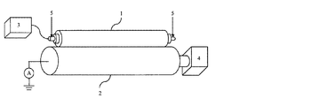
次に、本発明の帯電ローラを用いた電子写真装置の例について説明する。また、図5に、本発明に係る帯電ローラ1を組み込んだ電子写真装置の一例になる概略構成を示す。
Next, an example of an electrophotographic apparatus using the charging roller of the present invention will be described. FIG. 5 shows a schematic configuration as an example of an electrophotographic apparatus incorporating the charging
図5において、符号6は電子写真感光体であり、所定の周速度で回転駆動される。感光体6は、回転過程において、帯電ローラ1により、その周面に正または負の所定電位の均一帯電を受け、次いでスリット露光やレーザービーム走査露光などの露光手段8からの画像露光光を受ける。こうして感光体6の周面に静電潜像が順次形成されていく。
In FIG. 5, reference numeral 6 denotes an electrophotographic photosensitive member, which is rotationally driven at a predetermined peripheral speed. In the rotation process, the photosensitive member 6 is uniformly charged with a predetermined positive or negative potential on its peripheral surface by the charging
形成された静電潜像は、次いで現像手段9によりトナー現像され、現像されたトナー像は、不図示の給紙部から、感光体6と転写手段10との間に感光体6の回転と同期取りされて給紙された転写材Pに、転写手段10により順次転写されていく。 The formed electrostatic latent image is then developed with toner by the developing means 9, and the developed toner image is rotated between the photosensitive member 6 and the transfer means 10 from a paper supply unit (not shown). The images are sequentially transferred by the transfer means 10 to the transfer material P that is fed in synchronization.
像転写を受けた転写材Pは、感光体面から分離されて定着手段12へ導入されて像定着を受けることにより複写物(コピー)として装置外へプリントアウトされる。 The transfer material P that has received the image transfer is separated from the photoreceptor surface, introduced into the fixing means 12, and subjected to image fixing, thereby being printed out as a copy (copy).
像転写後の感光体6の表面は、クリーニング手段11によって転写残りトナーの除去を受けて清浄面化され、繰り返し像形成に使用される。
The surface of the photoreceptor 6 after the image transfer is cleaned by the
上述の感光体6、帯電ローラ1、現像手段9およびクリーニング手段11などの構成要素のうち、複数のものを一体に結合して構成し、複写機やレーザービームプリンターなどの電子写真装置本体に対して着脱可能なプロセスカートリッジとしてもよい。たとえば、現像手段9およびクリーニング手段11を感光体6および帯電ローラ1と共に一体に支持してカートリッジ化して、装置本体のレールなどの案内手段を用いて装置本体に着脱可能なプロセスカートリッジとすることができる。
Among the constituent elements such as the photosensitive member 6, the charging
また、画像露光光は、電子写真装置が複写機やプリンターである場合には、以下のようなものである。(1)原稿からの反射光や透過光。(2)センサーで原稿を読取り、信号化し、この信号に従って行われるレーザービームの走査、LEDアレイの駆動および液晶シャッターアレイの駆動などにより照射される光。 The image exposure light is as follows when the electrophotographic apparatus is a copying machine or a printer. (1) Reflected light or transmitted light from a document. (2) Light irradiated by scanning a laser beam, driving an LED array, driving a liquid crystal shutter array, and the like performed by reading a document with a sensor and converting the signal into a signal.
本発明に係る電子写真装置は、上述のように、以下の構成要素を具備する。
(1)電子写真感光体。(2)電子写真感光体の表面を本発明に係る帯電ローラにより帯電する帯電手段。(3)電子写真感光体を露光して潜像を形成する潜像形成手段。(4)トナーを感光体上に供給する現像手段。(5)感光体上のトナー像を被転写体に転写する転写手段。(6)感光体上の転写残トナーをクリーニングするクリーニング手段。(7)トナー像が形成された被転写体を定着する手段。
The electrophotographic apparatus according to the present invention includes the following components as described above.
(1) An electrophotographic photoreceptor. (2) Charging means for charging the surface of the electrophotographic photosensitive member with the charging roller according to the present invention. (3) Latent image forming means for exposing the electrophotographic photosensitive member to form a latent image. (4) Developing means for supplying toner onto the photoreceptor. (5) Transfer means for transferring the toner image on the photosensitive member to the transfer target. (6) Cleaning means for cleaning the transfer residual toner on the photosensitive member. (7) A means for fixing the transfer body on which the toner image is formed.
電子写真感光体としては、以下の二種類の感光体を採用するのが望ましい。
(1)珪素原子を主成分とする非晶質材料で形成した光導電層有する電子写真感光体
(2)表面保護層と感光層の合計の層厚が20μm以下の有機感光体
上記(1)としては、例えばアルミニウム(Al)、ステンレスなどの導電性材料からなる基体上に、光導電層および表面保護層を順次積層したものである。なお、これら層の他に、阻止層、反射防止層ないし界面層などの種々の機能層を必要に応じて設けてもよい。例えば、阻止層、界面層などを設けそのドーパントをIII族元素、V族元素など選択することにより、正帯電、負帯電といった帯電極性の制御も可能となる。本発明に係る電子写真装置においては、帯電性生成物による画像ボケ等の画像不良の観点から、正帯電性のシリコンドラムが望ましい。
As the electrophotographic photoreceptor, it is desirable to employ the following two types of photoreceptors.
(1) An electrophotographic photosensitive member having a photoconductive layer formed of an amorphous material mainly containing silicon atoms (2) An organic photosensitive member having a total thickness of the surface protective layer and the photosensitive layer of 20 μm or less (1) For example, a photoconductive layer and a surface protective layer are sequentially laminated on a base made of a conductive material such as aluminum (Al) or stainless steel. In addition to these layers, various functional layers such as a blocking layer, an antireflection layer, or an interface layer may be provided as necessary. For example, by providing a blocking layer, an interface layer and the like and selecting a dopant such as a group III element or a group V element, it is possible to control the charging polarity such as positive charging and negative charging. In the electrophotographic apparatus according to the present invention, a positively chargeable silicon drum is desirable from the viewpoint of image defects such as image blur due to a chargeable product.
基体形状は電子写真感光体の駆動方式などに応じた所望のものとしてよい。基体材質としては上記Alやステンレスのような導電性材料が一般的であるが、例えば各種のプラスチックやセラミックスなど、特には導電性を有しないものにこれら導電性材料を蒸着するなどして導電性を付与したものも用いることができる。 The substrate shape may be as desired according to the driving method of the electrophotographic photosensitive member. As the base material, conductive materials such as Al and stainless are generally used. However, for example, various conductive materials such as various plastics and ceramics, particularly those having no conductivity, are deposited to be conductive. Those provided with can also be used.
光導電層としては、シリコン原子が水素原子およびハロゲン原子を含む非晶質材料(「a―Si(H,X)」と略記する)が挙げられる。また、光導電層の層厚としては特に限定はないが、製造コストなどを考慮すると、15〜50μm程度が適当である。さらに、特性を向上させるために下部光導電層と上部光導電層のように複数の層構成にしてもよい。特に、半導体レーザーのように、比較的長い波長であって且つ波長バラツキのほとんどない光源に対しては、こうした層構成の工夫によって画期的な効果が現れる。 Examples of the photoconductive layer include an amorphous material in which silicon atoms include hydrogen atoms and halogen atoms (abbreviated as “a-Si (H, X)”). Further, the thickness of the photoconductive layer is not particularly limited, but about 15 to 50 μm is appropriate in consideration of the manufacturing cost. Furthermore, in order to improve the characteristics, a plurality of layers may be formed such as a lower photoconductive layer and an upper photoconductive layer. In particular, for a light source having a relatively long wavelength and almost no wavelength variation, such as a semiconductor laser, an epoch-making effect appears by devising such a layer structure.
表面保護層は、一般的にa―SiC(H,X)で形成されるが、a―C(H,X)としてもよい。また、光導電層と表面保護層の界面組成を連続的に変化させ、当該部分の界面反射を抑制させるように制御することが好ましい。 The surface protective layer is generally formed of a-SiC (H, X), but may be a-C (H, X). Further, it is preferable to control so that the interface reflection between the photoconductive layer and the surface protective layer is continuously changed to suppress the interface reflection of the portion.
上記(2)としては、例えばAl、ステンレスなどの導電性材料からなる基体上に導電性層、中間層、感光層、表面保護層をこの順に設けてなる電子写真感光体である。 The above (2) is an electrophotographic photosensitive member in which a conductive layer, an intermediate layer, a photosensitive layer, and a surface protective layer are provided in this order on a substrate made of a conductive material such as Al or stainless steel.
導電性層の結着樹脂としては、熱硬化性フェノール樹脂が好ましい。 The binder resin for the conductive layer is preferably a thermosetting phenol resin.
中間層としては、導電性層から感光層への電荷注入を阻止するために、中間層の体積抵抗率を1×10⁹〜1×10¹³Ω・cmに設定することが好ましい。非結晶性の共重合性ナイロンなどが好ましい。中間層の膜厚は0.1〜2μmであることが好ましい。 As the intermediate layer, the volume resistivity of the intermediate layer is preferably set to 1 × 10 9 to 1 × 10 13 Ω · cm in order to prevent charge injection from the conductive layer to the photosensitive layer. Non-crystalline copolymerizable nylon and the like are preferable. The film thickness of the intermediate layer is preferably 0.1 to 2 μm.
感光層は、電荷輸送物質と電荷発生物質を同一の層に含有する単層型感光層であっても、電荷発生物質を含有する電荷発生層と電荷輸送物質を含有する電荷輸送層とに分離した積層型感光層であってもよい。電子写真特性の観点から積層型感光層の方が好ましい。また、積層型感光層には支持体側から電荷発生層、電荷輸送層の順に積層した順層型感光層と、支持体側から電荷輸送層、電荷発生層の順に積層した逆層型感光層があるが、電子写真特性の観点から順層型感光層が好ましい。感光層の膜厚は、15μm以下であることが望ましい。 The photosensitive layer is separated into a charge generating layer containing a charge generating material and a charge transporting layer containing a charge transporting material even if it is a single layer type photosensitive layer containing the charge transporting material and the charge generating material in the same layer. The laminated photosensitive layer may be used. From the viewpoint of electrophotographic characteristics, the laminated photosensitive layer is preferred. The laminated photosensitive layer includes a normal layer type photosensitive layer laminated in the order of the charge generation layer and the charge transport layer from the support side, and a reverse layer type photosensitive layer laminated in the order of the charge transport layer and the charge generation layer from the support side. However, a normal photosensitive layer is preferred from the viewpoint of electrophotographic characteristics. The film thickness of the photosensitive layer is desirably 15 μm or less.
表面保護層としては、不飽和二重結合を有する連鎖重合性化合物を、感光層上に塗布後硬化することで形成される。連鎖重合性化合物は熱でも硬化反応を行うこともできるが、紫外線あるいは電子線などを使用して硬化することも可能である。保護層の膜厚は1〜5μmであること望ましい。 The surface protective layer is formed by applying a chain polymerizable compound having an unsaturated double bond onto the photosensitive layer and then curing it. The chain polymerizable compound can be cured by heat, but can also be cured using ultraviolet rays or electron beams. The thickness of the protective layer is desirably 1 to 5 μm.
潜像形成手段としては、半導体レーザーを用いたレーザー露光装置を採用するのが好ましい。また、潜像形成方式については、例えば、アモルファスシリコン感光体を用いる場合にはバックスキャン方式を、薄膜有機感光体を用いる場合にはイメージスキャン方式を採用するのが好ましい。 As the latent image forming means, a laser exposure apparatus using a semiconductor laser is preferably employed. As for the latent image forming method, for example, it is preferable to adopt a back scan method when an amorphous silicon photoconductor is used, and an image scan method when a thin film organic photoconductor is used.
現像手段としては、アモルファスシリコン感光体の場合は、現像キャリアを用いた2成分現像方式を用いるのが好ましい。 As the developing means, in the case of an amorphous silicon photoreceptor, it is preferable to use a two-component developing system using a developing carrier.
トナーはスチレン共重合体、エステルワックスを含有する粉砕トナーで負帯電性である。また、外添剤としては酸化チタン、シリカ、チタン酸ストロンチウムを用いるのが好ましい。 The toner is a pulverized toner containing a styrene copolymer and an ester wax, and is negatively charged. Further, it is preferable to use titanium oxide, silica, or strontium titanate as the external additive.
キャリアとしては、磁性分散型キャリア粒子を用いるのが望ましい。現像方式に関しては、アモルファスシリコン感光体を用いた電子写真装置の場合は、正帯電感光体と負帯電性トナーを用いた正規現像方式を、薄膜有機感光体の電子写真装置の場合は、現像キャリアを用いた2成分現像方式を採用するのが好ましい。 As the carrier, it is desirable to use magnetic dispersion type carrier particles. Regarding the developing system, in the case of an electrophotographic apparatus using an amorphous silicon photoconductor, a regular developing system using a positively charged photoconductor and a negatively chargeable toner is used. In the case of an electrophotographic apparatus using a thin film organic photoconductor, a developing carrier is used. It is preferable to adopt a two-component development system using
トナーは、結着樹脂、着色剤、そして、必要に応じてその他の添加剤を含む着色樹脂粒子と、コロイダルシリカ微粉末のような外添剤が外添されている着色粒子とを有している。そして、トナーは、負帯電性のポリエテスル系樹脂であり、重量平均粒子径(D4)は5μm以上かつ8μm以下が好ましい。 The toner includes colored resin particles containing a binder resin, a colorant, and other additives as necessary, and colored particles to which an external additive such as colloidal silica fine powder is externally added. Yes. The toner is a negatively charged polyethylene resin, and the weight average particle diameter (D4) is preferably 5 μm or more and 8 μm or less.
キャリアは、例えば表面酸化或は未酸化の鉄、ニッケル、コバルト、マンガン、クロム、希土類などの金属、及びそれらの合金、或は酸化物フェライトなどが好適に使用可能であり、これらの磁性粒子の製造法は特に制限されない。そして、キャリアは、重量平均粒子径(D4)が20〜50μm、好ましくは30〜40μmであり、抵抗率が107Ωcm以上、好ましくは108Ωcm以上である。 As the carrier, for example, surface-oxidized or non-oxidized iron, nickel, cobalt, manganese, chromium, rare earth and other metals, and their alloys, or oxide ferrite can be preferably used. The production method is not particularly limited. The carrier has a weight average particle diameter (D4) of 20 to 50 μm, preferably 30 to 40 μm, and a resistivity of 10 7 Ωcm or more, preferably 10 8 Ωcm or more.
本発明における薄膜有機感光体を用いた電子写真装置の現像方式は、負帯電感光体と負帯電性トナーを用いた正規現像方式である。転写手段としては、転写ローラを用いて被転写体(紙・OHP等のメディア)に直接転写する転写手段か、または転写ベルト等の中間転写体に一次転写する転写手段を用いるのが好ましい。 The developing system of the electrophotographic apparatus using the thin film organic photoreceptor in the present invention is a regular developing system using a negatively charged photoreceptor and a negatively chargeable toner. As the transfer unit, it is preferable to use a transfer unit that directly transfers to a transfer target (paper, medium such as OHP) using a transfer roller, or a transfer unit that primarily transfers to an intermediate transfer member such as a transfer belt.
クリーニング手段としては、ブレード状の部材によるブレードクリーニングや、ブラシ状の部材によるブラシクリーニング、その両方を用いる方法を用いるのが好ましい。 As the cleaning means, it is preferable to use a blade cleaning method using a blade-shaped member, a brush cleaning method using a brush-shaped member, or a method using both.
帯電ローラとしては、導電層を形成するベースポリマーが少なくともアクリルニトリル−ブタジエンゴムで構成され、かつ、そのアクリロニトリル含有率が34%超49%未満である電子ローラが好ましい。電子写真装置の使用環境が高温高湿環境となった場合、通常の環境に比べて帯電ローラの通電劣化はより厳しくなる。したがって、帯電ローラの導電層の分子運動性はより低い方が好ましく、アクリロニトリル含有率が34%超49%未満であることが望ましい。 As the charging roller, an electronic roller in which the base polymer forming the conductive layer is composed of at least acrylonitrile-butadiene rubber and the acrylonitrile content is more than 34% and less than 49% is preferable. When the electrophotographic apparatus is used in a high-temperature and high-humidity environment, the deterioration of energization of the charging roller becomes more severe than in a normal environment. Therefore, the molecular mobility of the conductive layer of the charging roller is preferably lower, and the acrylonitrile content is preferably more than 34% and less than 49%.
以下に本発明を製造例と実施例に沿って説明するが、本発明はその要旨を超えない限り、これらに限定されるものではない。 The present invention will be described below with reference to production examples and examples, but the present invention is not limited to these unless it exceeds the gist.
「実施例1」
(帯電ローラの作製)
下記の各材料を混合し、加圧ニーダーで30分混練した(表1参照)。
・アクリルニトリル−ブタジエンゴム(JSR社製:商品名「N215SL」、結合アクリロニトリル48%)(以下、NBR1と略す):100質量部。
・亜鉛華:5質量部。
・ステアリン酸亜鉛:1質量部。
・可塑剤:10質量部。
・炭酸カルシウム(丸尾カルシウム社製:商品名「ナノックス#30」):20質量部。
・カーボンブラック1(ケッチェンブラックインターナショナル社製:商品名「ケッチェンブラックEC600JD」、平均粒径40nm):4質量部。
・カーボンブラック2(旭カーボン株式会社製:商品名「アサヒサーマル」、平均粒径80nm):40質量部。
"Example 1"
(Production of charging roller)
The following materials were mixed and kneaded with a pressure kneader for 30 minutes (see Table 1).
Acrylonitrile-butadiene rubber (manufactured by JSR: trade name “N215SL”, bonded acrylonitrile 48%) (hereinafter abbreviated as NBR1): 100 parts by mass.
-Zinc flower: 5 mass parts.
-Zinc stearate: 1 part by mass.
-Plasticizer: 10 mass parts.
Calcium carbonate (manufactured by Maruo Calcium Co., Ltd .: trade name “Nanox # 30”): 20 parts by mass.
Carbon black 1 (manufactured by Ketjen Black International Co., Ltd .: trade name “Ketjen Black EC600JD”, average particle size 40 nm): 4 parts by mass.
Carbon black 2 (Asahi Carbon Co., Ltd .: trade name “Asahi Thermal”, average particle size 80 nm): 40 parts by mass.
その後、硫黄2質量部と加硫促進剤TMTM(大内新興化学工業株式会社製、テトラチウラムモノスルフィド)2質量部を加え、更に15分間オープンロールで混練した。このゴム混合物をゴム押し出し機で、円筒形に押し出し、長さ400mmに裁断し、加硫缶を使用して160℃で40分間一次加硫し、導電層の一次加硫チューブを得た。 Thereafter, 2 parts by mass of sulfur and 2 parts by mass of vulcanization accelerator TMTM (manufactured by Ouchi Shinsei Chemical Co., Ltd., tetrathiuram monosulfide) were added, and the mixture was further kneaded with an open roll for 15 minutes. This rubber mixture was extruded into a cylindrical shape with a rubber extruder, cut into a length of 400 mm, and primary vulcanized at 160 ° C. for 40 minutes using a vulcanizing can to obtain a primary vulcanized tube of a conductive layer.
次に、SUS製導電性支持体(図1(A))の表面に熱硬化性接着剤を塗布し、それを得られた一次加硫チューブに挿入し、その後、電気オーブンを用いて160℃で1時間、二次加硫と接着剤の硬化を行い、未研磨の導電層を導電性支持体上に形成した。この未研磨の導電層の長さが320mmとなるようにその両端部を切断した後、導電層表面を回転砥石で研磨した。次いで、研磨後の導電層の表面に、低圧水銀ランプ(ハリソン東芝ライティング製)を用いて紫外線を5分間照射して、UV処理(紫外線積算光量:約6000mJ/cm2)した。なお、この低圧水銀ランプは主に254nmの波長の紫外線を発するものである。以上のようにして実施例1の帯電ローラを得た(図1(B))。なお、図1には、実施形態の一例として寸法を記載したが、特に限定されるものではない。 Next, a thermosetting adhesive is applied to the surface of the conductive support made of SUS (FIG. 1A) and inserted into the resulting primary vulcanization tube, and then 160 ° C. using an electric oven. Then, secondary vulcanization and curing of the adhesive were carried out for 1 hour to form an unpolished conductive layer on the conductive support. Both ends were cut so that the length of the unpolished conductive layer was 320 mm, and then the surface of the conductive layer was polished with a rotating grindstone. Next, the surface of the conductive layer after polishing was irradiated with ultraviolet rays for 5 minutes using a low-pressure mercury lamp (manufactured by Harrison Toshiba Lighting), and UV treatment (ultraviolet ray integrated light amount: about 6000 mJ / cm 2 ) was performed. This low-pressure mercury lamp mainly emits ultraviolet light having a wavelength of 254 nm. As described above, the charging roller of Example 1 was obtained (FIG. 1B). In addition, although the dimension was described in FIG. 1 as an example of embodiment, it is not specifically limited.
完成した帯電ローラの表面を目視で、亀裂の有無を評価した。亀裂を目視で確認できない場合は○、亀裂を目視で確認できる場合は×とした。亀裂の評価において×となった帯電ローラに関しては、その後の評価を行わなかった。実施例1の帯電ローラにおける亀裂の評価は○であった。 The surface of the completed charging roller was visually evaluated for the presence of cracks. In the case where the crack could not be confirmed visually, it was marked as ◯, and in the case where the crack could be confirmed visually, it was marked as x. Subsequent evaluation was not performed on the charging roller that was evaluated as x in the crack evaluation. The evaluation of cracks in the charging roller of Example 1 was good.
「実施例2」
カーボンブラック処方をカーボンブラック1とカーボンブラック3(Cancarb社製、N990、平均粒径230nm)の混合系に変えて、配合量をそれぞれ3.4質量部、40質量部に変えた(表1参照)。それ以外は、実施例1と同様の方法で、帯電ローラを作製した。亀裂の評価は○であった。
"Example 2"
The carbon black formulation was changed to a mixed system of
「実施例3」
カーボンブラック処方をカーボンブラック1のみとし、その配合量を4.5質量部に変えた以外は(表1参照)、実施例1と同様の方法で、帯電ローラを作製した。亀裂の評価は○であった。
"Example 3"
A charging roller was produced in the same manner as in Example 1 except that
「実施例4」
NBR1をアクリルニトリル−ブタジエンゴム(JSR社製:商品名「N232S」、結合アクリロニトリル35%)(以下、NBR2と略す)に変えて、カーボンブラック配合量をそれぞれ2.8質量部、60質量部に変えた(表1参照)。それ以外は、実施例1と同様の方法で、帯電ローラを作製した。亀裂の評価は○であった。
Example 4
NBR1 is changed to acrylonitrile-butadiene rubber (manufactured by JSR: trade name “N232S”, bonded acrylonitrile 35%) (hereinafter abbreviated as NBR2), and the carbon black content is 2.8 parts by mass and 60 parts by mass, respectively. Changed (see Table 1). Other than that, a charging roller was produced in the same manner as in Example 1. The evaluation of the crack was ○.
「実施例5」
NBR1をNBR2に、カーボンブラック処方をカーボンブラック1とカーボンブラック3の混合系に変えて、カーボンブラック配合量をそれぞれ2.2質量部、60質量部に変えた以外は(表1参照)、実施例1と同様の方法で、帯電ローラを作製した。亀裂の評価は○であった。
"Example 5"
Except for changing NBR1 to NBR2 and changing the carbon black formulation to a mixed system of
「実施例6」
NBR1をNBR2に、カーボンブラック処方をカーボンブラック1のみとし、その配合量を4.6質量部に変えた以外は(表1参照)、実施例1と同様の方法で、帯電ローラを作製した。亀裂の評価は○であった。
"Example 6"
A charging roller was produced in the same manner as in Example 1 except that NBR1 was changed to NBR2, the carbon black formulation was changed to
「実施例7」
NBR1をアクリルニトリル−ブタジエンゴム(JSR社製:商品名「N240S」、結合アクリロニトリル26%)(以下、NBR3と略す)に変えて、カーボンブラックの配合量をそれぞれ3.8質量部、40質量部に変えた(表1参照)。それ以外は、実施例1と同様の方法で、帯電ローラを作製した。亀裂の評価は○であった。
"Example 7"
NBR1 is changed to acrylonitrile-butadiene rubber (manufactured by JSR: trade name “N240S”, 26% bonded acrylonitrile) (hereinafter abbreviated as NBR3), and the amount of carbon black is 3.8 parts by mass and 40 parts by mass, respectively. (See Table 1). Other than that, a charging roller was produced in the same manner as in Example 1. The evaluation of the crack was ○.
「実施例8」
NBR1をNBR3に、カーボンブラック処方をカーボンブラック1とカーボンブラック3の混合系に変えて、カーボンブラック配合量をそれぞれ3.2質量部、40質量部に変えた(表1参照)。それ以外は、実施例1と同様の方法で、帯電ローラを作製した。亀裂の評価は○であった。
"Example 8"
NBR1 was changed to NBR3, the carbon black formulation was changed to a mixed system of
「実施例9」
NBR1をNBR3に、カーボンブラック処方をカーボンブラック1のみとし、その配合量を4.6質量部に変えた以外は(表1参照)、実施例1と同様の方法で、帯電ローラを作製した。亀裂の評価は○であった。
"Example 9"
A charging roller was produced in the same manner as in Example 1 except that NBR1 was changed to NBR3, the carbon black formulation was changed to
「比較例1」
NBR1をアクリルニトリル−ブタジエンゴム(JSR社製:商品名「N640」、結合アクリロニトリル25%)(以下、NBR5と略す)に変えて、カーボンブラックの配合量をそれぞれ3.4質量部、40質量部に変えた(表1参照)。それ以外は、実施例1と同様の方法で、帯電ローラを作製した。亀裂の評価は○であった。
“Comparative Example 1”
NBR1 is changed to acrylonitrile-butadiene rubber (manufactured by JSR: trade name “N640”, 25% bonded acrylonitrile) (hereinafter abbreviated as NBR5), and the amount of carbon black is 3.4 parts by mass and 40 parts by mass, respectively. (See Table 1). Other than that, a charging roller was produced in the same manner as in Example 1. The evaluation of the crack was ○.
「比較例2」
NBR1をNBR5に、カーボンブラック処方をカーボンブラック1とカーボンブラック3の混合系に変えて、カーボンブラック配合量をそれぞれ3.6質量部、40質量部に変えた以外は(表1参照)、実施例1と同様の方法で、帯電ローラを作製した。亀裂の評価は○であった。
“Comparative Example 2”
Except that NBR1 was changed to NBR5, the carbon black formulation was changed to a mixed system of
「比較例3」
NBR1をNBR5に、カーボンブラック処方をカーボンブラック1のみとし、その配合量を4.3質量部に変えた以外は(表1参照)、実施例1と同様の方法で、帯電ローラを作製した。亀裂の評価は○であった。
“Comparative Example 3”
A charging roller was produced in the same manner as in Example 1 except that NBR1 was changed to NBR5, the carbon black formulation was changed to
「比較例4」
NBR1をヒドリン(ダイソー社製:商品名「エピクロマーCG102」)に変えて、カーボンブラック配合量をそれぞれ1.4質量部、40質量部に変えた以外は(表1参照)、実施例1と同様の方法で、帯電ローラを作製した。亀裂の評価は○であった。
“Comparative Example 4”
Except for changing NBR1 to hydrin (Daiso Co., Ltd .: trade name “Epichromer CG102”) and changing the amount of carbon black to 1.4 parts by mass and 40 parts by mass, respectively (see Table 1), the same as Example 1 In this way, a charging roller was produced. The evaluation of the crack was ○.
「比較例5」
NBR1をヒドリンに、カーボンブラック処方をカーボンブラック1とカーボンブラック3の混合系に変えて、カーボンブラック配合量をそれぞれ0.9質量部、40質量部に変えた以外は(表1参照)、実施例1と同様の方法で、帯電ローラを作製した。亀裂の評価は○であった。
“Comparative Example 5”
Except for changing NBR1 to hydrin and changing the carbon black formulation to a mixed system of
「比較例6」
NBR1をヒドリンに、カーボンブラック処方をカーボンブラック1のみとし、その配合量を2.5質量部に変えた以外は(表1参照)、実施例1と同様の方法で、帯電ローラを作製した。亀裂の評価は○であった。
“Comparative Example 6”
A charging roller was produced in the same manner as in Example 1 except that NBR1 was hydrin, the carbon black formulation was only
「比較例7」
NBR1をアクリルニトリル−ブタジエンゴム(日本ゼオン社製:商品名「NipolDN003」、結合アクリロニトリル50%)(以下、NBR4と略す)に変えて、カーボンブラックの配合量をそれぞれ3.5質量部、40質量部に変えた(表1参照)。それ以外は、実施例1と同様の方法で、帯電ローラを作製した。亀裂の評価は×であった。
“Comparative Example 7”
NBR1 is changed to acrylonitrile-butadiene rubber (manufactured by Zeon Corporation: trade name “NipolDN003”, bonded acrylonitrile 50%) (hereinafter abbreviated as NBR4), and the blending amounts of carbon black are 3.5 parts by mass and 40 parts by mass, respectively. (See Table 1). Other than that, a charging roller was produced in the same manner as in Example 1. The evaluation of the crack was x.
「比較例8」
NBR1をNBR4に、カーボンブラック処方をカーボンブラック1とカーボンブラック3の混合系に変えて、カーボンブラック配合量をそれぞれ3.8質量部、40質量部に変えた以外は(表1参照)、実施例1と同様の方法で、帯電ローラを作製した。亀裂の評価は×であった。
“Comparative Example 8”
Except that NBR1 was changed to NBR4, the carbon black formulation was changed to a mixed system of
「比較例9」
NBR1をNBR4に、カーボンブラック処方をカーボンブラック1のみとし、その配合量を4.1質量部に変えた以外は(表1参照)、実施例1と同様の方法で、帯電ローラを作製した。亀裂の評価は×であった。
"Comparative Example 9"
A charging roller was produced in the same manner as in Example 1 except that NBR1 was changed to NBR4, the carbon black formulation was changed to

NBR2:JSR社製N232S(結合アクリロニトリル35%)、
NBR3:JSR社製N240S(結合アクリロニトリル26%)、
NBR4:日本ゼオン社製NipolDN003(結合アクリロニトリル50%)、
NBR5:JSR社製N640(結合アクリロニトリル25%)、
ヒドリン:ダイソー社製エピクロマーCG102、
カーボンブラック1:ケッチェンブラックEC600JD(平均粒径40nm)、
カーボンブラック2:アサヒサーマル(平均粒径80nm)、
カーボンブラック3:MTカーボンN990(平均粒径230nm)。
NBR2: J232 N232S (bonded acrylonitrile 35%),
NBR3: N240S manufactured by JSR (26% bonded acrylonitrile),
NBR4: Nipol DN003 (bound acrylonitrile 50%) manufactured by Nippon Zeon Co., Ltd.
NBR5: N640 manufactured by JSR (bound acrylonitrile 25%),
Hydrin: Daiso Epichromer CG102,
Carbon black 1: Ketjen black EC600JD (average particle size 40 nm),
Carbon black 2: Asahi thermal (average particle size 80 nm),
Carbon black 3: MT carbon N990 (average particle size 230 nm).
(T2の測定)
T2の測定には、実施例1乃至9、比較例1乃至6で作製した帯電ローラの導電層を削り取ったもの(UV処理した表面を除く)を試料として供した。測定装置は日本電子株式会社製(商品名:MU25A)パルスNMR装置を用いた。T2の値は、パルスNMR測定により水素核を測定核とし、ソリッドエコー法を用いて得られたエコー強度Sから求める。測定条件は、測定周波数20MHz、90°パルス幅(Pw1)2.0μsec、パルス間隔(Pi1)=12μsec、温度23℃とし、ソリッドエコー法(90°xτ90°y)を用いた。観測されたエコー強度Sから最小2乗法によりT2を求める。観測されるエコー強度Sは次式(1)で与えられる。
(Measurement of T 2 )
The measurement of T 2, and subjected Examples 1 to 9, which scraped the conductive layer of the charging roller prepared in Comparative Examples 1 to 6 (excluding UV treated surface) as a sample. The measuring apparatus used was a JEOL Ltd. (trade name: MU25A) pulse NMR apparatus. The value of T 2 is obtained from the echo intensity S obtained using the solid echo method with a hydrogen nucleus as a measurement nucleus by pulse NMR measurement. The measurement conditions were a measurement frequency of 20 MHz, a 90 ° pulse width (Pw1) of 2.0 μsec, a pulse interval (Pi1) = 12 μsec, a temperature of 23 ° C., and a solid echo method (90 ° x τ90 ° y ) was used. T 2 is obtained from the observed echo intensity S by the least square method. The observed echo intensity S is given by the following equation (1).
S(t)= Σ S0iexp(−t/T2i) (1)
ここで、tは時間(τ)、S0iは各i成分のt=0におけるエコー強度、またT2iは各i成分のT2を表し、Σはiについての合計を表す。例えば、i成分の数が3であった場合、エコー強度Sは次式(2)で与えられる。
S (t) = ΣS 0i exp (−t / T 2i ) (1)
Here, t represents time (τ), S 0i represents the echo intensity at t = 0 of each i component, T 2i represents T 2 of each i component, and Σ represents the sum for i. For example, when the number of i components is 3, the echo intensity S is given by the following equation (2).
S(t)= S0Sexp(−t/T2S)+S0Mexp(−t/T2M)+S0Lexp(−t/T2L) (2)
各成分S、M、Lの関係は、T2S<T2M<T2Lであり、また、導電層中における各成分の分率がS0S、S0M、S0Lの比で与えられる。従って、導電層のT2の平均値は、次式(3)で与えられる。
S (t) = S 0S exp (−t / T 2S ) + S 0M exp (−t / T 2M ) + S 0L exp (−t / T 2L ) (2)
The relationship between the components S, M, and L is T 2S <T 2M <T 2L , and the fraction of each component in the conductive layer is given by the ratio of S 0S , S 0M , and S 0L . Therefore, the average value of T 2 of the conductive layer is given by the following equation (3).
T2= (S0S×T2S+S0M×T2M+S0L×T2L)/ ΣS0 (3)
(ΣS0=S0S+S0M+S0L)
成分iの数については、導電層に含有されるベースポリマーや添加物(カーボンブラック等)の種類や添加量によって異なる。本実施例においては、成分iの数は、2または3であった。
T 2 = (S 0S × T 2S + S 0M × T 2M + S 0L × T 2L ) / ΣS 0 (3)
(ΣS 0 = S 0S + S 0M + S 0L)
About the number of the components i, it changes with kinds and addition amount of the base polymer and additive (carbon black etc.) which are contained in a conductive layer. In this example, the number of component i was 2 or 3.
実施例1乃至9、比較例1乃至6で作製した帯電ローラの導電層についてT2を測定した結果を表2に示す。 Table 2 shows the results of measuring T 2 for the conductive layers of the charging rollers prepared in Examples 1 to 9 and Comparative Examples 1 to 6.
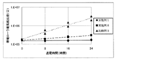
(通電劣化指数の測定)
図2に示す装置に、実施例1乃至9、比較例1乃至6で作製した帯電ローラを取り付け、室温低湿環境(N/L:23℃/5%RH)において通電劣化加速試験を行い、通電劣化指数を求めた。図2に示す装置は、帯電ローラ1をアルミドラム2に当接し、帯電バイアス電源3から直流+交流電流を供給しながら、ドラム駆動モーター4でアルミドラムを駆動させて、バネ加圧5で固定した帯電ローラを回転させる装置である。
(Measurement of energization degradation index)
The charging roller produced in Examples 1 to 9 and Comparative Examples 1 to 6 is attached to the apparatus shown in FIG. 2, and an energization deterioration acceleration test is performed in a room temperature and low humidity environment (N / L: 23 ° C./5% RH). The degradation index was determined. In the apparatus shown in FIG. 2, the charging
通電条件としては、直流電流290μA、交流総電流3.3mA、8時間/1日で3日間通電させた。 As energization conditions, a DC current of 290 μA, an AC total current of 3.3 mA, and 8 hours / 1 day were energized for 3 days.
帯電ローラの電気抵抗値を、以下の7回測定し、時間毎にプロットした電気抵抗値を図3に示した。
(1)1日目通電前、(2)1日目8時間通電後(8時間後)、(3)2日目通電前(8時間朝)、(4)2日目8時間通電後(16時間後)、(5)3日目通電前(16時間朝)、(6)3日目8時間通電後(24時間後)、(7)4日目朝(24時間朝)。尚、8時間後と8時間朝、16時間後と16時間朝、24時間後と24時間朝に関しては、それぞれ8、16、24の同時間にプロットした。また、次式(4)を用いてフィッティングした(図3)。
The electric resistance value of the charging roller was measured seven times as follows, and the electric resistance value plotted for each time is shown in FIG.
(1) Before energization on the first day, (2) After energization for 8 hours on the first day (after 8 hours), (3) Before energization on the second day (8 hours in the morning), (4) After energization for 8 hours on the second day ( 16 hours later), (5) Before the third day energization (16 hours morning), (6) After the
R(電気抵抗値:Ω)=R0×exp(0.0001×A×T) (4)
〔R(電気抵抗測定値:Ω)、R0(初期電気抵抗値:Ω)、A(通電劣化指数)、T(時間)〕
通電劣化の指標として、通電劣化指数(A)の値を用いた。Aの評価としては、
◎:0<|A|(Aの絶対値)<100:通電劣化が非常に良好である。
○:100≦|A|≦220:通電劣化が実用に耐えることのできるレベルである。
×:220<|A|:通電劣化が悪化して、実用に耐えることのできるレベルでない。
とした。
R (electric resistance value: Ω) = R 0 × exp (0.0001 × A × T) (4)
[R (Measured electrical resistance value: Ω), R 0 (Initial electrical resistance value: Ω), A (Electrical degradation index), T (Time)]
The value of the power deterioration index (A) was used as an index of power deterioration. As an evaluation of A,
A: 0 <| A | (Absolute value of A) <100: Deterioration of energization is very good.
○: 100 ≦ | A | ≦ 220: Deterioration of energization is a level that can withstand practical use.
×: 220 <| A |: Deterioration of energization deteriorates and is not at a level that can withstand practical use.
It was.
実施例1乃至9、比較例1乃至6で作製した帯電ローラについて通電劣化指数を評価した結果を表2に示す。 Table 2 shows the results of evaluating the energization deterioration index of the charging rollers manufactured in Examples 1 to 9 and Comparative Examples 1 to 6.
なお、電気抵抗値(Ω)は、以下の方法により求めた。
アルミドラム2と帯電ローラ1の接触面積が均一になるように導電性支持体5の両端部に300gの加重をかけつつ、アルミドラム2を回転させて帯電ローラを従動回転させながら、300Vの直流電圧をアルミドラムと導電性支持体との間に印加し、その間に流れる電流を測定することにより求めた(図4)。
The electrical resistance value (Ω) was determined by the following method.
While applying 300 g of weight to both ends of the
(通紙耐久試験によるドラム電位の安定性評価)
(1)アモルファスシリコン感光体(a−Si)を用いた通紙耐久試験
キヤノン社製複写機GP405を改造し、実施例1乃至9、比較例1乃至6で作製した帯電ローラを取り付けた。また、複写機のプロセス速度を400mm/sに設定し、帯電バイアスは外部電源から供給した。帯電条件はDC電圧+600V、AC電圧1.5kV、AC周波数3.5kHzとした。露光方式は、バックスキャン方式に変更した。現像手段は、感光体ドラム(アモルファスシリコン感光体)にあわせて下記に示したものを用いた。
(Evaluation of drum potential stability by paper endurance test)
(1) Paper passing durability test using amorphous silicon photoconductor (a-Si) The Canon copier GP405 was remodeled, and the charging rollers produced in Examples 1 to 9 and Comparative Examples 1 to 6 were attached. The process speed of the copying machine was set to 400 mm / s, and the charging bias was supplied from an external power source. The charging conditions were a DC voltage of +600 V, an AC voltage of 1.5 kV, and an AC frequency of 3.5 kHz. The exposure method was changed to the back scan method. As the developing means, those shown below according to the photosensitive drum (amorphous silicon photosensitive member) were used.
実施例1乃至9、比較例1乃至6で作製した帯電ローラとアモルファスシリコン感光体を搭載して、室温低湿環境(N/L:23℃/5%RH)において、上記条件にて、通紙耐久試験(25万枚印刷)を行い、試験前後のドラム電位の低下について評価した。結果を表2に示す。また、ドラム電位の評価方法を以下に示す。
○:通紙耐久試験前後のドラム電位を測定し、ドラム電位の低下が認められない。
×:通紙耐久試験中にドラム電位の低下が発生した。
The charging roller prepared in Examples 1 to 9 and Comparative Examples 1 to 6 and the amorphous silicon photoconductor are mounted, and paper is passed under the above conditions in a room temperature and low humidity environment (N / L: 23 ° C./5% RH). A durability test (printing 250,000 sheets) was performed, and the decrease in drum potential before and after the test was evaluated. The results are shown in Table 2. The drum potential evaluation method is shown below.
○: The drum potential before and after the paper passing durability test was measured, and no decrease in drum potential was observed.
X: A decrease in drum potential occurred during the paper passing durability test.
アモルファスシリコン感光体については、正帯電のa−Si系感光体として、Alからなる導電性支持体の表面に順次積層させたもので、負電荷阻止層、光導電層、表面保護層から構成される感光体ドラムを用いた。 The amorphous silicon photoconductor is a positively charged a-Si type photoconductor that is sequentially laminated on the surface of a conductive support made of Al, and is composed of a negative charge blocking layer, a photoconductive layer, and a surface protective layer. A photosensitive drum was used.
トナーとしては、スチレン共重合体にエステルワックス、着色剤を分散させた負帯電性の粉砕トナーを用い、外添剤としては、シリカ、酸化チタン、チタン酸ストロンチウムを用いた。トナーの重量平均粒子径(D4)は6.8μmであった。 As the toner, a negatively charged pulverized toner in which an ester wax and a colorant are dispersed in a styrene copolymer was used, and silica, titanium oxide, and strontium titanate were used as external additives. The weight average particle diameter (D4) of the toner was 6.8 μm.
キャリアとしては、フェノール樹脂にマグネタイトを分散させた磁性粒子分散型キャリア粒子を用いた。キャリアの重量平均粒子径(D4)は35μm、抵抗率は109Ωcmであった。 As the carrier, magnetic particle-dispersed carrier particles in which magnetite was dispersed in a phenol resin were used. The carrier had a weight average particle diameter (D4) of 35 μm and a resistivity of 10 9 Ωcm.
現像手段は、現像キャリアを用いた2成分現像方式を用いた。 As the developing means, a two-component developing system using a developing carrier was used.
(2)薄膜有機感光体(薄膜OPC)を用いた通紙耐久試験
帯電条件をDC電圧−750V、AC電圧2.0kV、AC周波数3.2kHzに、露光方式をイメージスキャン方式に変更し、薄膜有機感光体を搭載した以外は、上記アモルファスシリコン感光体を用いた通紙耐久試験と同様の方法で通紙耐久試験を行った。結果を表2に示す。
(2) Paper-passing durability test using a thin-film organic photoreceptor (thin film OPC) The charging conditions were changed to the DC voltage -750 V, the AC voltage 2.0 kV, the AC frequency 3.2 kHz, the exposure method to the image scan method, and the thin film A paper passing durability test was performed in the same manner as the paper passing durability test using the amorphous silicon photosensitive member except that the organic photosensitive member was mounted. The results are shown in Table 2.
ここで、薄膜有機感光体は、アルミシリンダー上に、電子輸送性有機化合物を含有する層厚1μmの中間層、層厚0.15μmのフタロシアニン系電荷発生層と層厚10μmのトリアリールアミン系電荷輸送層で構成される感光層、層厚5μmの光重合性保護層を有する感光体である。 Here, the thin-film organic photoreceptor has an intermediate layer containing an electron-transporting organic compound on an aluminum cylinder, a 1 μm thick intermediate layer, a 0.15 μm thick phthalocyanine charge generating layer, and a 10 μm thick triarylamine charge. It is a photoreceptor having a photosensitive layer composed of a transport layer and a photopolymerizable protective layer having a layer thickness of 5 μm.
トナーはシリカと酸化チタンを外添した負帯電性のポリエテスル系樹脂に着色剤としてカーボンブラックを分散させた粉砕トナーを用いた。トナーの重量平均粒子径(D4)は7.0μmであった。 The toner used was a pulverized toner in which carbon black was dispersed as a colorant in a negatively charged polyethylene resin externally added with silica and titanium oxide. The weight average particle diameter (D4) of the toner was 7.0 μm.
キャリアは、酸化物フェライトを使用した。キャリアの重量平均粒子径(D4)は30μmであり、抵抗率は108Ωcmであった。現像手段は、現像キャリアを用いた2成分現像方式を用いた。 The carrier used oxide ferrite. The carrier had a weight average particle diameter (D4) of 30 μm and a resistivity of 10 8 Ωcm. As the developing means, a two-component developing system using a developing carrier was used.
1 帯電ローラ
2 アルミドラム
3 帯電バイアス電源(AC+DC)
4 ドラム駆動モーター
5 バネ加圧
6 電子写真感光体
7 軸
8 露光手段
9 現像手段
10 転写手段
11 クリーニング手段
12 定着手段
P 転写材
1 Charging
4
Claims (2)
該帯電ローラが、
導電性支持体と該導電性支持体上に形成された導電層とを有し、
該導電層が、ベースポリマーとしてのアクリロニトリル−ブタジエンゴムと導電性粒子としてのカーボンブラックとを含み、
該アクリロニトリル−ブタジエンゴムは、アクリロニトリル含有率が25%超49%未満であることを特徴とする電子写真装置。 A photoreceptor having a photoconductive layer formed of an amorphous material mainly composed of silicon atoms, a charging roller in contact with or close to the photoreceptor, and forming a latent image by exposing an image Means, a developing means for forming a toner image on the photosensitive member, and a transferring means for transferring the toner image to the transfer member, and applying a direct current and an alternating current between the photosensitive member and the charging roller. In an electrophotographic apparatus for charging the surface of the photoreceptor by
The charging roller is
A conductive support and a conductive layer formed on the conductive support;
The conductive layer includes acrylonitrile-butadiene rubber as a base polymer and carbon black as conductive particles,
The acrylonitrile-butadiene rubber has an acrylonitrile content of more than 25% and less than 49%.
Priority Applications (1)
| Application Number | Priority Date | Filing Date | Title |
|---|---|---|---|
| JP2007162431A JP5201886B2 (en) | 2007-06-20 | 2007-06-20 | Electrophotographic equipment |
Applications Claiming Priority (1)
| Application Number | Priority Date | Filing Date | Title |
|---|---|---|---|
| JP2007162431A JP5201886B2 (en) | 2007-06-20 | 2007-06-20 | Electrophotographic equipment |
Publications (3)
| Publication Number | Publication Date |
|---|---|
| JP2009003082A JP2009003082A (en) | 2009-01-08 |
| JP2009003082A5 JP2009003082A5 (en) | 2010-08-05 |
| JP5201886B2 true JP5201886B2 (en) | 2013-06-05 |
Family
ID=40319559
Family Applications (1)
| Application Number | Title | Priority Date | Filing Date |
|---|---|---|---|
| JP2007162431A Active JP5201886B2 (en) | 2007-06-20 | 2007-06-20 | Electrophotographic equipment |
Country Status (1)
| Country | Link |
|---|---|
| JP (1) | JP5201886B2 (en) |
Families Citing this family (2)
| Publication number | Priority date | Publication date | Assignee | Title |
|---|---|---|---|---|
| JP5312568B2 (en) | 2011-12-26 | 2013-10-09 | キヤノン株式会社 | Conductive member, process cartridge, and electrophotographic apparatus |
| KR102016204B1 (en) * | 2015-10-08 | 2019-08-29 | 캐논 가부시끼가이샤 | Electrophotographic electro-conductive member, method of producing the same, process cartridge, and electrophotographic apparatus |
Family Cites Families (6)
| Publication number | Priority date | Publication date | Assignee | Title |
|---|---|---|---|---|
| JPH0552857U (en) * | 1991-12-18 | 1993-07-13 | ブラザー工業株式会社 | Charging roller |
| JPH1165269A (en) * | 1997-08-25 | 1999-03-05 | Sumitomo Rubber Ind Ltd | Conductive rubber composition and conductive elastic roller using the rubber composition |
| JP3967450B2 (en) * | 1998-02-24 | 2007-08-29 | 東海ゴム工業株式会社 | Charging roll |
| JP4144701B2 (en) * | 2003-03-14 | 2008-09-03 | シンジーテック株式会社 | Charging roll |
| JP3879862B2 (en) * | 2005-05-24 | 2007-02-14 | 株式会社リコー | Image forming method |
| JP4197181B2 (en) * | 2005-07-06 | 2008-12-17 | キヤノン化成株式会社 | Conductive rubber roller |
-
2007
- 2007-06-20 JP JP2007162431A patent/JP5201886B2/en active Active
Also Published As
| Publication number | Publication date |
|---|---|
| JP2009003082A (en) | 2009-01-08 |
Similar Documents
| Publication | Publication Date | Title |
|---|---|---|
| KR101552897B1 (en) | Charging member, charging device, process cartridge, and image forming apparatus | |
| KR101201135B1 (en) | Charging member, process cartridge, and electrophotographic apparatus | |
| JP2007219087A (en) | Electrifying device and image forming apparatus | |
| JP5962136B2 (en) | Image forming apparatus | |
| JP2011069906A (en) | Electrophotographic photoreceptor, image forming apparatus, and process cartridge | |
| JP2010076205A (en) | Method of manufacturing conductive roller, conductive roller, charged roller, and electrophotographic device | |
| JP5201886B2 (en) | Electrophotographic equipment | |
| JP2013186342A (en) | Electrophotographic photoreceptor, process cartridge, and image forming apparatus | |
| JP2005134515A (en) | Electrophotographic photoreceptor, process cartridge, image forming apparatus and method for forming image | |
| JP6894346B2 (en) | Image forming device | |
| JP5499782B2 (en) | Image forming apparatus | |
| JP2011022425A (en) | Electrophotographic photoreceptor, process cartridge, and image forming apparatus | |
| JP4400366B2 (en) | Electrophotographic photosensitive member and method for manufacturing the same, electrophotographic apparatus, and process cartridge | |
| JP5935700B2 (en) | Image forming apparatus, image forming method, and process cartridge | |
| JP2012103627A (en) | Flange member, photoreceptor drum, process cartridge, image forming device and image forming method | |
| JP2011203306A (en) | Electrophotographic photoreceptor, image forming apparatus and process cartridge | |
| JP2011085621A (en) | Image forming apparatus | |
| JP2011133690A (en) | Image forming apparatus | |
| JP2010060609A (en) | Charging roller and electrophotographic apparatus | |
| JP5377024B2 (en) | Method for manufacturing charging member | |
| JP5504626B2 (en) | Image forming apparatus and process cartridge | |
| JP5994322B2 (en) | Method for manufacturing charging member | |
| JP4159901B2 (en) | Charging member and image forming apparatus | |
| JP2009186965A (en) | Method for determining adhesion force distribution, method for determining powder removing characteristic, image carrier, blade, cleaning device, and image forming device | |
| JP2008026414A (en) | Cleaning roll for charging member, charging device, process cartridge and image forming apparatus |
Legal Events
| Date | Code | Title | Description |
|---|---|---|---|
| A521 | Written amendment |
Free format text: JAPANESE INTERMEDIATE CODE: A523 Effective date: 20100621 |
|
| A621 | Written request for application examination |
Free format text: JAPANESE INTERMEDIATE CODE: A621 Effective date: 20100621 |
|
| TRDD | Decision of grant or rejection written | ||
| A01 | Written decision to grant a patent or to grant a registration (utility model) |
Free format text: JAPANESE INTERMEDIATE CODE: A01 Effective date: 20130115 |
|
| A61 | First payment of annual fees (during grant procedure) |
Free format text: JAPANESE INTERMEDIATE CODE: A61 Effective date: 20130212 |
|
| R151 | Written notification of patent or utility model registration |
Ref document number: 5201886 Country of ref document: JP Free format text: JAPANESE INTERMEDIATE CODE: R151 |
|
| FPAY | Renewal fee payment (event date is renewal date of database) |
Free format text: PAYMENT UNTIL: 20160222 Year of fee payment: 3 |