JP5201872B2 - Ink jet recording head and method for storing information in ink jet recording head - Google Patents
Ink jet recording head and method for storing information in ink jet recording head Download PDFInfo
- Publication number
- JP5201872B2 JP5201872B2 JP2007120810A JP2007120810A JP5201872B2 JP 5201872 B2 JP5201872 B2 JP 5201872B2 JP 2007120810 A JP2007120810 A JP 2007120810A JP 2007120810 A JP2007120810 A JP 2007120810A JP 5201872 B2 JP5201872 B2 JP 5201872B2
- Authority
- JP
- Japan
- Prior art keywords
- recording head
- fuse element
- ink jet
- fuse
- jet recording
- Prior art date
- Legal status (The legal status is an assumption and is not a legal conclusion. Google has not performed a legal analysis and makes no representation as to the accuracy of the status listed.)
- Active
Links
Images


Description
本発明は、インクジェット記録ヘッド用基板、該基板を搭載するインクジェット記録ヘッドに関するものである。 The present invention relates to an ink jet recording head substrate and an ink jet recording head on which the substrate is mounted.
インクジェット記録装置は、インクジェット記録ヘッドからインクを吐出して記録を行う所謂ノンインパクト記録方式の記録装置であり、高速な記録が可能であること、様々な記録媒体に対応が可能であること、騒音がほとんど生じないことなどの特徴をもつ。このようなことから、インクジェット記録装置は、プリンタ、複写機、ファクシミリ、ワードプロセッサ等の記録機構を担う装置として広く採用されている。 The ink jet recording apparatus is a so-called non-impact recording type recording apparatus that performs recording by ejecting ink from an ink jet recording head, and is capable of high-speed recording, compatible with various recording media, noise It has the feature that almost does not occur. For this reason, the ink jet recording apparatus is widely adopted as an apparatus that bears a recording mechanism such as a printer, a copier, a facsimile machine, and a word processor.
インクジェット記録ヘッド(以下、単に記録ヘッドともいう)は、種々の方式により吐出するインク滴を形成するものが知られている。その中でも、インク吐出のためのエネルギとして熱を利用する記録ヘッドは、高密度のマルチノズル化を比較的容易に実現でき、高解像度、高画質で高速な記録が可能である。 Ink jet recording heads (hereinafter also simply referred to as recording heads) are known that form ink droplets that are ejected by various methods. Among them, a recording head that uses heat as energy for ink ejection can relatively easily realize a high-density multi-nozzle, and can perform high-resolution and high-quality recording at high speed.
記録ヘッドはインクジェット記録装置に交換可能に取り付けられて記録を行うものが多い。このような記録ヘッドに、記録ヘッド自身のID(Identity)コードやインク吐出機構の駆動特性といった記録ヘッド固有の情報を読み出し自在に記憶させるため、記録ヘッド基体にROM(Resd Only Memory)を搭載することがある。この機能は、インクジェット記録装置本体に着脱可能な記録ヘッドを用いる場合、記録時にその記録ヘッド固有の情報を得て最適な駆動を行う上で非常に有効な手段である。 Many recording heads are attached to an ink jet recording apparatus in a replaceable manner to perform recording. In such a recording head, a ROM (Res Only Memory) is mounted on the recording head base so that information specific to the recording head such as an ID (Identity) code of the recording head and driving characteristics of the ink ejection mechanism can be read out. Sometimes. This function is a very effective means for performing optimum driving by obtaining information specific to a recording head at the time of recording when a recording head that can be attached to and detached from the ink jet recording apparatus main body is used.
例えば、記録ヘッドにEEPROM(Electrically Erasable Programmable ROM)を搭載することが特許文献1に開示されている。しかし特許文献1の記録ヘッドは、記録ヘッド基体上ではなく記録ヘッドとは別体に構成されたEEPROMを搭載しているため、構造が複雑になるうえ生産性も良好ではなく、装置の小型軽量化も阻害している。さらに、このようなROMは大容量の情報を記憶させるには有用であるが、記憶させるべき情報が大容量でない場合にはコスト的に不利となる。
For example,
また、特許文献2には、記録ヘッドを製造するにあたり、ROMとして機能するヒューズ素子を同時に形成することが開示されている。このヒューズ素子を、適宜溶断しておき、使用時にその溶断の有無を読み取り可能とすることにより、2値データを保持するROMとして機能させることができる。このような記録ヘッドは、ヘッド固有の情報を保持させながらも構造の簡略化、生産性の向上、コストの削減および小型軽量化をも実現することができる。 Japanese Patent Application Laid-Open No. H10-228688 discloses that a fuse element that functions as a ROM is formed simultaneously when a recording head is manufactured. The fuse element is appropriately blown out so that the presence or absence of the blowout can be read at the time of use so that the fuse element can function as a ROM holding binary data. Such a recording head can realize the simplification of the structure, the improvement of productivity, the reduction of cost, and the reduction in size and weight while retaining the information unique to the head.
このように、記録ヘッドの基板にヒューズ素子を組み込む場合、記録ヘッドには記録中にインクが付着するため、ヒューズ素子の溶断部分にインクが侵入した場合にその溶断部分が腐食したり、ヒューズ素子の電極が腐食して信頼性が損なわれるおそれがある。そのため、インクジェット基板にヒューズ素子が作り込まれる場合は、ヒューズ素子の部分にインクが侵入しない構造としなければならない。そこで、記録ヘッド用基板においてインク吐出機構やヒューズ素子が形成される層は、その上部に他の層が形成されることで下層部に位置するものとなっている。 As described above, when the fuse element is incorporated in the substrate of the recording head, the ink adheres to the recording head during recording. Therefore, when the ink enters the fusing part of the fuse element, the fusing part is corroded or the fuse element. The electrodes may corrode and reliability may be impaired. For this reason, when a fuse element is formed on an ink jet substrate, a structure in which ink does not enter the fuse element portion must be provided. Therefore, the layer in which the ink ejection mechanism and the fuse element are formed on the recording head substrate is positioned in the lower layer portion by forming another layer on the upper layer.
特許文献2で用いられているヒューズ素子を溶断する方法として、レーザ光を用いたものがある。この方法は、ヒューズ素子を溶断、蒸発させて電気的に開路状態にする最も効果的な方法である。しかし、ヒューズ素子が溶断したときに発生する溶出物が基板上に付着したり、また溶断工程においてコストが掛かる等の点から、この方法は大量生産には適さない。 As a method for fusing the fuse element used in Patent Document 2, there is a method using laser light. This method is the most effective method for electrically opening the fuse element by fusing and evaporating. However, this method is not suitable for mass production because the eluate generated when the fuse element is melted adheres to the substrate and the cost is high in the melting process.
また別の溶断方法として、ヒューズ素子にパルス波の電流を流すことで溶断させる方法もある。この方法はコストが掛からず、しかも溶出物が基板上へ付着することも少ないため大量生産に適している。しかし、ヒューズ素子に立ち上がりの大きなパルス波の電流を流して溶断した場合、ヒューズの溶断部の間隔が狭くなり、ヒューズ素子周囲の樹脂層もあまり溶けない。よって、溶けたヒューズ材料の飛散を許容するための空間が殆ど無く、溶断後も溶けたヒューズ材料が同じ空間に存在するため、再度接続されてしまうおそれがある。 As another fusing method, there is a method of fusing by supplying a pulse wave current to the fuse element. This method is suitable for mass production because it does not cost much and the effluent hardly adheres to the substrate. However, when the fuse element is blown by flowing a large rising pulse wave current, the interval between the fused portions of the fuse is narrowed, and the resin layer around the fuse element is not melted so much. Therefore, there is almost no space for allowing the melted fuse material to scatter, and the melted fuse material exists in the same space even after fusing, so that there is a possibility that it will be reconnected.
そこで、記録ヘッド用基板に搭載されたヒューズ素子を確実に溶断させるために、記録ヘッド用基板の外部(装置本体側)に抵抗素子を設けて、ヒューズ素子の溶断時に、立ち上がりの小さなパルス波の電流が流れるように電流を調整する方法がある。このようにして立ち上がりの小さなパルス波の電流を用いてヒューズを溶断すると、ヒューズ溶断部の間隔は広いものとなり、ヒューズ素子周囲の樹脂層も溶ける。よって溶断時に溶けたヒューズ材料が飛散を許容する十分な空間が形成されて、溶断部の間隔も広くなることから、溶断部が再度接続されてしまうことも無く、信頼性の高い開路状態を実現することができる。 Therefore, in order to surely blow the fuse element mounted on the recording head substrate, a resistance element is provided outside the recording head substrate (on the apparatus main body side). There is a method of adjusting the current so that the current flows. When the fuse is blown using a pulse wave current having a small rise in this way, the interval between the fuse blown portions becomes wide, and the resin layer around the fuse element is also melted. Therefore, a sufficient space that allows the melted fuse material to scatter is formed and the interval between the fusing parts is widened, so that the fusing parts are not reconnected and a highly reliable open circuit state is realized. can do.
しかし、ヒューズを溶断させるのに最適な電流波形は、個々のヒューズ素子毎にばらつきがある。記録ヘッド用基板の外部(装置本体側)に抵抗素子を設けた場合、その抵抗素子は固定の抵抗であり、交換可能な記録ヘッドの個々のヒューズ素子毎のばらつきに対応していない。したがって、記録ヘッドと装置本体の組み合わせによっては、ヒューズ素子の溶断が十分に行われないおそれがある。 However, the optimum current waveform for fusing the fuse varies from one fuse element to another. When a resistance element is provided outside the recording head substrate (on the apparatus main body side), the resistance element is a fixed resistance and does not correspond to variations among individual fuse elements of the replaceable recording head. Therefore, depending on the combination of the recording head and the apparatus main body, the fuse element may not be sufficiently melted.
よって本発明は、確実にヒューズ素子の溶断が行われるようにすることで、信頼性高く情報を記録することができるインクジェット記録ヘッド用基板、該基板を搭載するインクジェット記録ヘッドを提供することを目的とする。 Accordingly, an object of the present invention is to provide an ink jet recording head substrate capable of recording information with high reliability by reliably fusing fuse elements, and an ink jet recording head mounting the substrate. And
そのため、本発明のインクジェット記録ヘッドへの情報記憶方法は、インクを吐出するために利用されるエネルギを発生する記録素子と、中央部分の幅は細く設けられ電流を流すことによって溶断し、溶断の有無によって情報を記憶可能なヒューズ素子と、該ヒューズ素子を溶断する際に流れる電流の抵抗となる抵抗素子と、を有する、インクジェット記録ヘッドへの情報記憶方法であって、前記ヒューズ素子に、当該ヒューズ素子と同一の薄膜層をパターニングすることで設けられた前記抵抗素子を介して電流を流すことにより、前記ヒューズ素子を溶断させることを特徴とする。 For this reason, the information storage method for the ink jet recording head of the present invention has a recording element that generates energy used for ejecting ink, and a central portion that is thin and melted by flowing current. An information storage method for an ink jet recording head, comprising: a fuse element capable of storing information depending on presence / absence; and a resistance element serving as a resistance of a current that flows when the fuse element is blown. The fuse element is blown by passing a current through the resistance element provided by patterning the same thin film layer as the fuse element.
本発明によれば、ヒューズ素子を溶断する電流が流れるロジック回路上であり、ヒューズ素子が設けられた層と同一層に、電流の調整手段を設けたことで、ヒューズ素子を溶断するのに適した電流に調整することが可能になる。したがって、インクジェット記録ヘッドに記録された情報の信頼性が高くなり、最適な吐出条件で記録を行うことができるインクジェット記録ヘッド用基板とインクジェット記録ヘッドを実現することができる。 According to the present invention, on a logic circuit through which a current for fusing the fuse element flows, the current adjusting means is provided in the same layer as the layer provided with the fuse element, so that the fuse element is suitable for fusing. It becomes possible to adjust to the current. Therefore, the reliability of the information recorded on the ink jet recording head is increased, and an ink jet recording head substrate and an ink jet recording head that can perform recording under optimum discharge conditions can be realized.
以下、図面を参照して本発明の一実施形態を説明する。
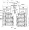
図1は、本実施形態のインクジェット記録ヘッド400(以下、単に記録ヘッドともいう)を搭載可能なシリアルスキャンタイプのインクジェット記録装置(以下、単に記録装置ともいう)300を示した斜視図である。本実施形態の記録装置300は、キャリッジ303に記録ヘッド400を搭載して、キャリッジ303が走査することで記録を行うものである。その記録ヘッド400には、後述する記録素子用基板H1110(図3参照)が組み込まれており、その記録素子用基板H1110の表面に、ヒータ素子H1103や配線が形成されている。さらに記録ヘッド400には、ヒューズ素子410および電流調整手段としての抵抗素子411が同一の薄膜層に同一材料で作り込まれている。また記録素子用基板H1110には、記録ヘッド400と外部の端子とを電気的に接続するための電極パッドH1104(a〜f)なども形成されている。
Hereinafter, an embodiment of the present invention will be described with reference to the drawings.
FIG. 1 is a perspective view showing a serial scan type ink jet recording apparatus (hereinafter also simply referred to as a recording apparatus) 300 on which an ink jet recording head 400 (hereinafter also simply referred to as a recording head) of the present embodiment can be mounted. The
記録ヘッド400は、ヘッド移動機構302のキャリッジ303に着脱自在に搭載され、キャリッジ303は、ガイドシャフト304等により矢印Xの主走査方向に移動自在に支持され、さらにヘッド移動機構302によって主走査方向に往復移動される。このように支持された記録ヘッド400と対向する位置には、記録媒体である記録用紙Pを保持して搬送するプラテンローラ305が配置されている。このプラテンローラ305等により記録用紙Pを矢印Yの副走査方向に順次搬送する用紙搬送機構306が構成されている。
The
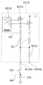
図2は、本実施形態の記録装置300の制御系を示すブロック図である。ヘッド移動機構302と用紙搬送機構306は、図2のように、移動制御回路311に接続されており、この移動制御回路311は、マイクロコンピュータ形態の制御部312に接続されている。この制御部312がヘッド移動機構302と用紙搬送機構306とを統合制御することにより、記録ヘッド400と記録用紙Pとが相対移動される。制御部312には、データ入力手段であるデータ入力回路313、データ読出手段であるデータ読出回路314および通信I/F315等も接続されている。この通信I/F315には、通信ケーブル220を介してホストコンピュータ形態などのホスト装置210が接続されている。
FIG. 2 is a block diagram illustrating a control system of the
データ入力回路313は、キャリッジ303の接続コネクタを介して記録ヘッド400の記録ロジック回路(図3参照)に接続されており、その記録ロジック回路に記録データを供給する。またデータ読出回路315は、キャリッジ303の接続コネクタを介して記録ヘッド400のヒューズロジック回路(図3参照)に接続されており、そのヒューズロジック回路から、後述するヒューズ素子410の記憶データを読み出す。
The
マイクロコンピュータ形態の制御部312は、上述のような各種回路311,313,314も統合制御する。例えば、ホスト装置210から通信I/F315に入力される記録データをデータ入力回路313に供給し、またデータ読出回路314が記録ヘッド400から読み出した記憶データを通信I/F315からホスト装置210に出力する。
The
本実施形態の記録装置300では、インク供給手段であるインクタンクは記録ヘッドと一体のカートリッジとして搭載されており、インクの使いきりに伴ってキャリッジ303に着脱自在となっている。インクタンクにはインクが充填されており、このインクが記録ヘッド400に供給される。
In the
図2において画像処理システム200は、中央制御装置であるホスト装置(ホストコンピュータ)210と、記録装置300と、によって構成される。記録装置300とホスト装置210とは通信ケーブル220によって接続されている。画像処理システム200は、例えば、ホスト装置210から供給される記録データに基づいて、記録装置300を記録動作させる。その際、制御部312の統合制御により、ヘッド移動機構302が記録ヘッド400を主走査方向に移動させると共に、用紙搬送機構306が記録用紙Pを副走査方向に搬送させる。これらの動作に同期して、データ入力回路313が記録ヘッド400に記録データを入力する。
In FIG. 2, the
記録ヘッド400は、インクタンクから常時供給されるインクを保持しており、記録データに基づいて、記録ヘッド400の記録ロジック回路が、後述する多数のヒータ素子H1103を選択的に発熱駆動する。この多数のヒータ素子H1103の選択的な発熱により、インクを発泡させて対応する吐出口からインク滴を吐出する。このインク滴が記録用紙Pの表面に付着することによって、画像を点配列で表現する、いわゆるドットマトリクスの画像が形成される。
The
図3は、本実施形態の記録装置300の記録素子用基板H1110に設けられたロジック回路を示した図である。本実施形態の記録ヘッド400には、図3に示す記録素子用基板H1110が組み込まれている。その記録素子用基板H1110上には、ヒータ素子H1103、ヒューズ素子410、電流調整手段としての抵抗素子411、電極パッドH1104(a〜f)、および配線等からなるロジック回路が形成されている。ヒータ素子H1103は、インクの吐出エネルギとしての熱エネルギを発生するものであり、インクを加熱して発泡させることにより、不図示の吐出口からインク滴を吐出させる。電極パッドH1104(a〜f)は、記録素子用基板H1110に形成された配線を外部端子と電気的に接続させるための電極を構成し、ヒータ素子H1103の駆動信号などが供給される。ヒューズ素子410は、電流によって溶断可能な複数のヒューズ素子410が形成されており、それぞれのヒューズ素子410を選択的に溶断することによって、種々のデータを記憶させることができる。電流調整手段としての抵抗素子411は、ヒューズ素子410を確実に溶断させ、その溶断の有無に応じてデータを高い信頼性をもって記憶させることができるようにその抵抗値が調整されている。インク供給口H1102は、記録素子用基板H1110の中心部に形成されており、その周辺にヒータ素子H1103が配置されている。
FIG. 3 is a diagram illustrating a logic circuit provided on the printing element substrate H1110 of the
また、図3のロジック回路は以下のように構成されている。本実施形態ではヒューズ素子410はポリシリコン抵抗体で形成されており、インク供給口H1102の短辺側に配置されている。ヒューズ素子410の溶断、読み出しをするために駆動する第2の駆動素子H1118は、第1の駆動素子H1116に隣接して配置されている。
Further, the logic circuit of FIG. 3 is configured as follows. In the present embodiment, the
第2の駆動素子H1118を選択する選択信号と第1の駆動素子H1116を選択する選択信号とは、ともに同じ信号系に構成されており、第1の駆動素子H1116を選択する論理回路と並列に第2の駆動素子H1118を選択する論理回路が接続されている。すなわち、第1の駆動素子H1116に選択信号を送る信号線、時分割駆動信号用のデコーダ(DECODER)、ラッチ回路(LT)、シフトレジスタ(S/R)および外部からの信号入力用パッド(不図示)は、第1および第2の駆動素子について共用されている。したがって、新規の信号線や配線領域や回路等を追加することなく、第2の駆動素子H1118を選択することができる。また、第2の駆動素子H1118をシフトレジスタ(S/R)等から出力された信号によって選択する選択回路H1112は、第1の駆動素子H1116の選択回路H1100と同様な形態である。なお、電気熱変換素子H1103にVH電源を供給するためのVH電源パッドH1104eからのびたVH電源配線H1114は電気熱変換素子H1103に接続されている。そして、GNDH電源を供給するためのGNDH電源パッドH1104fからのびたGNDH電源配線H1113は、電気熱変換素子H1103に接続された第1の駆動素子H1116とヒューズ素子410に接続された第2の駆動素子H1118とが共用している。
The selection signal for selecting the second drive element H1118 and the selection signal for selecting the first drive element H1116 are both configured in the same signal system, and in parallel with the logic circuit for selecting the first drive element H1116. A logic circuit for selecting the second driving element H1118 is connected. That is, a signal line for sending a selection signal to the first drive element H1116, a time-division drive signal decoder (DECODER), a latch circuit (LT), a shift register (S / R), and an external signal input pad (not used) (Shown) is shared by the first and second drive elements. Therefore, the second drive element H1118 can be selected without adding a new signal line, wiring region, circuit, or the like. A selection circuit H1112 that selects the second drive element H1118 by a signal output from a shift register (S / R) or the like has the same form as the selection circuit H1100 of the first drive element H1116. Note that the VH power supply wiring H1114 extending from the VH power supply pad H1104e for supplying the VH power to the electrothermal conversion element H1103 is connected to the electrothermal conversion element H1103. A GNDH power supply wiring H1113 extending from the GNDH power supply pad H1104f for supplying the GNDH power supply is connected to the electrothermal transducer H1103 and the second drive element H1118 connected to the
このように構成された記録素子用基板H1110の上層に、インクを供給および吐出させるための流路および吐出口の構成部材を有機樹脂層によって形成することができる。また記録素子用基板H1110の下部に、インク供給口H1102にインクを供給するためのインク供給部を連結する等して、インクジェット記録ヘッド400を完成させる。
In the upper layer of the recording element substrate H1110 configured as described above, the flow path for supplying and discharging ink and the constituent members of the discharge port can be formed of the organic resin layer. The ink
記録ヘッド400がヒューズ素子410を備えているため、例えば、記録ヘッド400の製造を完了して出荷する以前の時点において、IDコードやヒータ素子H1103の動作特性などに関するデータをヒューズ素子410に記録することができる。これは、例えば図2に示した画像処理システム200と同様の構成の検査システムを用いて行うことができる。
Since the
このようなデータを記録してから出荷された記録ヘッド400は、キャリッジ303に装着されて使用に供される。その際、記録装置300は、記録ヘッド400のヒューズ素子410の記憶データをデータ読出回路314によって読み出すことができる。したがって記録装置300は、記録ヘッド400のヒューズ素子410から読み出したヒータ素子H1103の動作特性に対応して、公知の制御を行うことが可能となる。例えば、ヒータ素子H1103に供給する駆動電力を調整したり、あるいは記録ヘッド400のIDコードをホスト装置210に通知したりすることができる。
The
次に、記録ヘッド400におけるヒューズ素子410および電流調整手段としての抵抗素子411の形成方法について説明する。
Next, a method for forming the
記録ヘッド400の製造にあたっては、記録素子用基板H1110に設ける駆動素子、ロジック回路等の半導体素子を積層状態に形成する時に用いられるゲート部のポリシリコンを使用して、ヒューズ素子410および抵抗素子411を以下のように作り込む。なお、ヒューズ素子410および抵抗素子411の形成の前に、予め、駆動素子、ロジック回路等の半導体素子が半導体製造工程を用いて作り込まれた基板を用いて、後から上層にヒューズ素子410および抵抗素子411を形成してもよい。
In manufacturing the
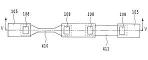
図4は、図3におけるヒューズ素子410と、そのヒューズ素子410に通電して溶断させるための電流が流れる回路中に存在する電流調整手段としての抵抗素子411とを示す拡大平面図である。このヒューズ素子410と抵抗素子411とが形成された層の上層に、インクを吐出するためのインクの流路が有機樹脂によって形成される。
FIG. 4 is an enlarged plan view showing the
図5は、図4のヒューズ素子および抵抗素子のV−Vにおける断面図である。 5 is a cross-sectional view taken along the line V-V of the fuse element and the resistance element of FIG.
図4において、ポリシリコンによって形成されるヒューズ素子410は、その中心部が細くなっている。例えば、その中心部は、長さ約10μm×幅約1.5μm程度に細長く形成されており、溶断しやすくなっている。ヒューズ素子410の端部はAl電極105に接続されている。スルーホール部108は、ヒューズ素子410とAl電極105とを接続するために設けられている。
In FIG. 4, the
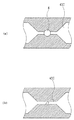
図5において、ヒューズ素子410は、記録素子用基板H1110の表面の熱酸化膜402上に積層された約4000Åのポリシリコンの膜からなる。このヒューズ素子410の上層には、層間絶縁膜としてSiO膜104がプラズマCVD法によって約8000Åの厚さに形成されている。このSiO膜104は、ポリシリコンのヒューズ素子410よりも融点が低く、ヒューズの溶断時の熱によって容易にガス化して空洞を形成する。SiO膜104の厚さは、ヒューズの溶断時にクラックが生じて大きく破壊することがないように、0.5〜1μmの範囲に設定することが望ましい。
In FIG. 5, the
次に、ヒューズ素子410の溶断時にSiO膜104に形成される空洞を制御するために、保護膜としてSiO膜104の上に組成の異なるSiO膜106をプラズマCVD法によって6000Å(0.6μm)の厚さに形成する。この保護膜106は、層間絶縁膜104よりも融点が高く、熱により容易に溶解しないような組成のために層間絶縁膜104の空洞の膨張を押さえて、それを所定の大きさに制御する。ただし、この保護膜106は、溶解のスピードは遅いものの、熱によって一部が溶けて穴を形成することにより、その穴から噴出物を放出させて、空洞の膨張を完全に押さえ込んだ場合の内部圧力によるクラックの発生を防止することができる。そのため、この保護膜106の厚さは、空洞の膨張を押さえ、かつ部分的に穴が生じるように、0.3〜0.8μmの範囲に設定することが望ましい。
Next, in order to control the cavity formed in the
このようにしてヒューズ素子410を形成した後、ヒータ素子H1103(図5参照)の材料としてのTaSiNをスパッタリング法によって約500Åの厚さに形成し、それに連続して、配線層としてAL層を約5000Åの厚さに形成する。それらをフォトリソグラフィ法によって所定の形状にパターニングし、BCl3ガスを用いたドライエッチングによって、AL層とTaSiN層を同時に所定の形状に形成する。さらに、ヒータ素子H1103の配置部分をフォトリソグラフィ法によって所定の形状にパターニングし、リン酸を主成分とするウエットエッチングによってヒータ素子H1103の配置部分を形成する。
After forming the
さらに、その上層に、プラズマCVD法によって、保護膜としてのSiN膜を約3000Åの厚さに形成し、さらにスパッタリング法によって、耐キャビテーション膜としてのTa膜を約2000Åの厚さに形成する。そして、フォトリソグラフィ法によって、それらのTa膜およびSiN膜をドライエッチングして、所定の形状とする。その際、ヒューズ素子410上のTa膜およびSiN膜は除去する。次に、フォトリソグラフィ法を用いて、インクを吐出するためのインク流路を有機樹脂層によって3次元的に形成する。以上のようにして、情報を記憶可能なヒューズ素子410を備えた記録ヘッド400の基板が完成する。
Further, a SiN film as a protective film is formed to a thickness of about 3000 mm by a plasma CVD method on the upper layer, and a Ta film as a cavitation-resistant film is formed to a thickness of about 2000 mm by a sputtering method. Then, the Ta film and the SiN film are dry-etched by a photolithography method to obtain a predetermined shape. At that time, the Ta film and the SiN film on the
図6は、ヒューズ素子410に接続される駆動回路を示した図である。ヒューズ素子410には、その溶融および情報の読み出しを行うための駆動素子H1118が接続されている。本実施形態の場合、複数のヒューズ素子410にはそれぞれに駆動素子H1118が個別に接続され、それらの駆動素子H1118は選択回路H1112によって選択的に駆動される。その選択回路H1112は、信号線、時分割選択信号(BLE)を発生するデコーダ(DECODER)、その他の信号を含む信号のラッチ回路(LT)、シフトレジスタ(S/R)、記録ヘッド基板の外部からの信号の入力パッド(図3参照)などを含む。この選択回路H1112は、複数のヒータ素子H1103(図3参照)を選択的に駆動するための回路と同様に構成されている。
FIG. 6 is a diagram showing a drive circuit connected to the
ヒューズ素子410を溶断する場合には、上記検査システム側に設けられたスイッチ503をオンにする。これによって、電源504の溶断電圧(例えば、ヒータ素子H1103の駆動電圧の24Vなど)を配線506からIDパッドH1104a(図では1つのみが示されているが、基板のレイアウト等により複数個備えることも可)に印加する。そして、駆動素子H1118を選択的に駆動することによって、それに対応するヒューズ素子410を溶断する。一方、ヒューズ素子410の溶断の有無に応じて記憶された情報を記録装置側に読み出す時は、複数のヒューズ素子410に対して共通に接続されるヒューズ読み出し用電源パッドH1104bに、電圧(例えばロジック回路の電源電圧の3.3Vなど)を印加する。そして、駆動素子H1118を選択的に駆動することによって、それに対応するヒューズ素子410の記憶情報、つまり溶断の有無に対応する信号を読み出す。
When fusing the
このように溶断電圧と読み出し電圧との間に明らかな電圧差を設定することにより、読み出し時間を制限することなく、しかもヒューズ素子410にダメージを与えることなく、記憶情報を読み出すことができる。その記憶情報の読み出しにおいて、溶断されているヒューズ素子410に対応する駆動素子H1118が駆動されたときには、IDパッドH1104aの出力信号がハイレベル(H)となる。また溶断されていないヒューズ素子410が駆動された時には、読み出し用電源パッドH1104bとの間に接続された読み出し抵抗H1111(ヒューズ素子410の抵抗値より大きな抵抗)によってIDパッドH1104aの出力信号がローレベル(L)になる。このようにして、1つのヒューズ素子には溶断の有無を確認することにより2値のデータを記憶させることができる。
By setting an obvious voltage difference between the fusing voltage and the read voltage in this way, the stored information can be read without limiting the read time and without damaging the
本実施形態においては、ヒューズ素子410を溶断させるための電流が流れる記録素子用基板H1110上の回路中に、ヒューズ溶断部と同一の薄膜層であるポリシリコン層により抵抗素子411が設けられている。例えば、この抵抗素子411は抵抗値が40〜120Ω程度であり、中央のテーパ部を含むヒューズ素子410の抵抗値は200〜410Ω、ヒューズ素子410を除きかつ抵抗素子411を含む回路の抵抗値は170〜330Ω程度である。本実施形態の場合、ヒューズ素子410の溶断に用いる電圧には、ヒータ素子H1103の駆動電圧と共通である24Vを用いる。
In the present embodiment, the
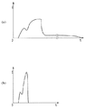
図7(a)、(b)は、異なるパルス波形の電流によって溶断したヒューズ素子の状態を示す図である。また、図8(a)、(b)は、異なるパルス波形を表わした図である。ヒューズ素子410を溶断させる電流が流れる回路に、本実施形態のような抵抗素子が設けられていない場合、つまりヒューズ素子に立ち上がりの大きなパルス幅の短い(図8(b))電流で溶断する場合、ヒューズ素子410の溶断部は図7(b)のようになる。この場合ヒューズ素子には大きな電流が流れて溶断するが、電流のパルス幅が狭い(ヒューズ素子への通電時間が短い)ため、ヒューズ素子周囲の樹脂層には熱が伝わりにくい。よってヒューズ素子周囲の樹脂層はほとんど溶けることなく、ヒューズだけが短く溶断することになる。その際、その溶断部は、溶断前のヒューズが占めていた分の空間が形成されており、溶けたヒューズ材料もその空間内に存在している。このように、溶融後の溶断部の幅が狭く、溶けたヒューズ材料の逃げ場所が無い(空間が狭い)状態になる溶断方法は、溶断後に再度接続されるおそれがあるため好ましくない。
FIGS. 7A and 7B are diagrams showing the state of the fuse element blown by currents having different pulse waveforms. FIGS. 8A and 8B are diagrams showing different pulse waveforms. When a resistance element as in this embodiment is not provided in a circuit through which a current for fusing the
また、本実施形態のように抵抗素子が設けられている場合、つまり、ヒューズ素子に時間的変化の緩やかな波形の電流を流して溶断する場合、ヒューズ素子410の溶断部は図7(a)のようになる。この場合、パルスの幅が広い(ヒューズ素子への通電時間が長い)ため、ヒューズ素子周囲の樹脂層にも十分に熱が伝わる。よってヒューズ素子周囲の樹脂層は溶けて図7(a)の空間Sのような広い空間を形成する。このように、溶断後の溶断部の幅が広い(空間が広い)状態になる溶断方法は、溶断後に再度接続するおそれも無く好ましい。
When the resistance element is provided as in the present embodiment, that is, when the fuse element is blown by supplying a current having a waveform with a gradual change in time, the blown portion of the
図9は、ヒューズ素子410を溶断させる電流が流れる回路上の、記録素子用基板H1110以外の部分に抵抗素子505が設けられた回路を示す図である。記録素子用基板H1110に設けられたヒューズ素子410の形状は、製造工程においてばらつくことが考えられ、それに伴って溶断する際に必要な電流も変わってくる。抵抗素子505が記録素子用基板H1110以外に設けられた場合、抵抗素子505の抵抗値をヒューズ素子410の形状のばらつきに対応させることができないため、溶断時にヒューズ素子410に適切な電流を流すことができないおそれがある。
FIG. 9 is a diagram showing a circuit in which a
図10は、ヒューズ素子の大きさと電流の関係を説明するための図であり、図10(a)は、比較的小さなヒューズ素子を表わした図であり、図10(b)は比較的大きなヒューズ素子を表わした図である。また、図11(a)、(b)もヒューズ素子の大きさと電流の関係を説明するための図であり、それぞれ図10(a)、(b)の側面からの断面図を表わしている。 FIG. 10 is a diagram for explaining the relationship between the size of the fuse element and the current, FIG. 10 (a) is a diagram showing a relatively small fuse element, and FIG. 10 (b) is a relatively large fuse. It is a figure showing an element. FIGS. 11A and 11B are also diagrams for explaining the relationship between the size of the fuse element and the current, and represent cross-sectional views from the side surfaces of FIGS. 10A and 10B, respectively.
図10(a)および図11(a)のように、ヒューズ素子が比較的小さくかつ薄い場合には、図8(a)のような波形の電流で、比較的長い時間をかけてゆっくりと溶断する必要がある。そのため、用いる抵抗素子は大きな抵抗値のものが必要になる。また、図10(b)および図11(b)のように、ヒューズ素子が比較的大きくかつ厚い場合には、図8(b)のような波形の電流で比較的短時間で溶断する必要がある。そのため、用いる抵抗素子は小さな抵抗値のものが必要になる。 As shown in FIGS. 10A and 11A, when the fuse element is relatively small and thin, it is blown slowly over a relatively long time with a current having a waveform as shown in FIG. There is a need to. Therefore, the resistance element to be used must have a large resistance value. Also, as shown in FIGS. 10B and 11B, when the fuse element is relatively large and thick, it needs to be blown in a relatively short time with a current having a waveform as shown in FIG. 8B. is there. Therefore, the resistance element to be used must have a small resistance value.
そこで、ヒューズ素子410の形状ばらつきによって異なる電流の最適な調整を有効に行うために、本実施形態のようにインクジェット記録ヘッドの記録素子用基盤H1110に、ヒューズ素子410の溶断部と同一の薄膜層に電流調整手段411を形成するとよい。同一の薄膜層にヒューズ素子410と抵抗素子411を形成することで、必然的にヒューズ素子410と抵抗素子411の厚さが等しく形成され、ヒューズ素子410を溶断させる電流を最適に調整することが可能な抵抗素子411を形成することができる。つまり、図10(a)および図11(a)に示すようなヒューズ溶断部410(a)が比較的細く薄い場合は、立ち上がりの穏やかな電流変化によって溶断される必要がある。そこで、抵抗素子411(a)を同じ層に形成することで、抵抗素子411(a)の膜厚も同時に薄くなるので溶断回路の電流調整手段としての抵抗が大きく、電流波形は緩やかになりヒューズ溶断の信頼性が確保できる。また、ヒューズ素子410を構成する薄膜層103(b)が比較的厚く形成されている記録ヘッドの場合には、電流調整手段として設けられる電気抵抗素子411(b)を構成する薄膜層も同時に厚くなる。このような比較的厚い膜で構成されたヒューズ溶断部は十分に大きな電流で溶断される必要があるが、膜が厚いことにより溶断回路の電流調整手段としての抵抗は少なくなるので、溶断後の信頼性を確保することができる。
Therefore, in order to effectively perform optimum adjustment of different currents due to variations in the shape of the
このように、インクジェット記録ヘッドに用いる記録素子用基板上に、ヒューズ素子を溶断する際の電流の調整を行う抵抗素子を設け、さらにヒューズ素子と同一層に抵抗素子を設けることで、ヒューズ素子を溶断するのに適した電流に調整することが可能になる。したがって、インクジェット記録ヘッドに記録された情報の信頼性が高くなり、最適な吐出条件で記録を行うことができるインクジェット記録ヘッド用基板とインクジェット記録ヘッドを実現することができた。 As described above, the resistance element for adjusting the current when fusing the fuse element is provided on the recording element substrate used in the ink jet recording head, and the resistance element is provided in the same layer as the fuse element. It becomes possible to adjust the current suitable for fusing. Therefore, the reliability of the information recorded on the ink jet recording head is improved, and an ink jet recording head substrate and an ink jet recording head capable of recording under optimum discharge conditions can be realized.
(その他の実施形態)
以下に本発明のその他の実施形態について説明する。
前述の実施形態では、1つの抵抗素子411が複数のヒューズ素子に対する抵抗の役割を担っていたが、本実施形態では、ヒューズ素子410それぞれに対応して個別に抵抗素子411を設けている。その他の構成は、前述の実施形態と同様である。
(Other embodiments)
Other embodiments of the present invention will be described below.
In the above-described embodiment, one
図12は、本実施形態の回路の構成を示す図である。図12に示すように、抵抗素子411は複数のヒューズ素子410のそれぞれに対応して個別に設けられている。この場合、ヒューズ素子410と抵抗素子411以外の回路が有する配線抵抗によらず、最適な溶断電流変化を個別のヒューズごとにもたらすことができるので、ヒューズ素子の基板内配置の自由度を上げることができる。
FIG. 12 is a diagram illustrating a configuration of a circuit according to the present embodiment. As shown in FIG. 12, the
また、図5で示したヒューズ素子410および抵抗素子411を形成する薄膜層103は、電気熱変換素子と同一の材料であって、TaSiN薄膜であっても同等の発明効果を得ることができる。
Further, the
また、ヒューズ素子410の溶断電流を流す回路は、記録装置とは別のヒューズ溶断装置に備えてもよく、この場合には、そのヒューズ溶断装置に記録ヘッド400を接続することにより、ヒューズ素子410を溶断して種々のデータを記憶させることができる。また、溶断電流を流すヒューズ素子410を選択するための選択回路H1112は、記録装置側に備えてもよい。また記録装置は、ヒューズ素子410の溶断の有無に対応するデータの読み出すための回路を備え、その回路の一部は記録ヘッド側に備えてもよい。
In addition, a circuit for supplying a fusing current of the
108 スルーホール部
210 ホスト装置
300 記録装置
400 記録ヘッド
410 ヒューズ素子
411 抵抗素子
505 抵抗素子
H1102 インク供給口
H1103 ヒータ素子
H1110 記録素子用基板
H1116 第1の駆動素子
H1118 第2の駆動素子
108 through-
Claims (10)
前記ヒューズ素子に、当該ヒューズ素子と同一の薄膜層をパターニングすることで設けられた前記抵抗素子を介して電流を流すことにより、前記ヒューズ素子を溶断させることを特徴とするインクジェット記録ヘッドへの情報記憶方法。 A recording element that generates energy used for ejecting ink, a fuse element that has a narrow central portion, is blown by flowing current, and can store information depending on whether or not fusing, and the fuse element A resistance element that becomes a resistance of a current that flows when fusing, and an information storage method for an ink jet recording head,
Information for an ink jet recording head, wherein the fuse element is blown by passing a current through the resistance element provided by patterning the same thin film layer as the fuse element to the fuse element. Memory method.
外部から前記端子に電圧が印加されることで、前記ヒューズ素子に前記抵抗素子を介して電流が流れることを特徴とする請求項1乃至請求項4のいずれか1項に記載のインクジェット記録ヘッドの情報記憶方法。 The inkjet recording head further includes a terminal used for applying a voltage to the fuse element and the resistance element,
5. The ink jet recording head according to claim 1, wherein when a voltage is applied to the terminal from the outside, a current flows to the fuse element through the resistance element. 6. Information storage method.
前記ヒューズ素子に、当該ヒューズ素子と同一の薄膜層をパターニングすることで設けられた前記抵抗素子を介して電流を流すことにより、前記ヒューズ素子を溶断させることを特徴とするインクジェット記録装置。 A recording element that generates energy used for ejecting ink, a fuse element that has a narrow central portion, is blown by flowing current, and can store information depending on whether or not fusing, and the fuse element An ink jet recording apparatus comprising an ink jet recording head having a resistance element that becomes a resistance of a current that flows when fusing,
An ink jet recording apparatus, wherein the fuse element is blown by passing a current through the resistance element provided by patterning the same thin film layer as the fuse element.
外部から前記端子に電圧が印加されることで、前記ヒューズ素子に前記抵抗素子を介して電流が流れることを特徴とする請求項6乃至請求項9のいずれか1項に記載のインクジェット記録装置。 The inkjet recording head further includes a terminal used for applying a voltage to the fuse element and the resistance element,
10. The ink jet recording apparatus according to claim 6, wherein a current flows to the fuse element through the resistance element when a voltage is applied to the terminal from the outside. 11.
Priority Applications (1)
| Application Number | Priority Date | Filing Date | Title |
|---|---|---|---|
| JP2007120810A JP5201872B2 (en) | 2007-05-01 | 2007-05-01 | Ink jet recording head and method for storing information in ink jet recording head |
Applications Claiming Priority (1)
| Application Number | Priority Date | Filing Date | Title |
|---|---|---|---|
| JP2007120810A JP5201872B2 (en) | 2007-05-01 | 2007-05-01 | Ink jet recording head and method for storing information in ink jet recording head |
Publications (3)
| Publication Number | Publication Date |
|---|---|
| JP2008273086A JP2008273086A (en) | 2008-11-13 |
| JP2008273086A5 JP2008273086A5 (en) | 2010-06-24 |
| JP5201872B2 true JP5201872B2 (en) | 2013-06-05 |
Family
ID=40051678
Family Applications (1)
| Application Number | Title | Priority Date | Filing Date |
|---|---|---|---|
| JP2007120810A Active JP5201872B2 (en) | 2007-05-01 | 2007-05-01 | Ink jet recording head and method for storing information in ink jet recording head |
Country Status (1)
| Country | Link |
|---|---|
| JP (1) | JP5201872B2 (en) |
Families Citing this family (1)
| Publication number | Priority date | Publication date | Assignee | Title |
|---|---|---|---|---|
| JP5578676B2 (en) * | 2010-09-29 | 2014-08-27 | 富士フイルム株式会社 | Droplet ejection apparatus and uncontrollable ejector wiring cutting method |
Family Cites Families (5)
| Publication number | Priority date | Publication date | Assignee | Title |
|---|---|---|---|---|
| JP4600652B2 (en) * | 2004-10-13 | 2010-12-15 | ヤマハ株式会社 | Semiconductor device and manufacturing method thereof |
| JP4457846B2 (en) * | 2003-10-24 | 2010-04-28 | ヤマハ株式会社 | Semiconductor device and manufacturing method thereof |
| JP2006108413A (en) * | 2004-10-06 | 2006-04-20 | Matsushita Electric Ind Co Ltd | Fuse and writing method using same |
| JP4604686B2 (en) * | 2004-11-29 | 2011-01-05 | ヤマハ株式会社 | Semiconductor device and manufacturing method thereof |
| JP4799298B2 (en) * | 2005-07-08 | 2011-10-26 | キヤノン株式会社 | Ink jet recording head manufacturing method, ink jet recording head, and ink jet recording apparatus |
-
2007
- 2007-05-01 JP JP2007120810A patent/JP5201872B2/en active Active
Also Published As
| Publication number | Publication date |
|---|---|
| JP2008273086A (en) | 2008-11-13 |
Similar Documents
| Publication | Publication Date | Title |
|---|---|---|
| US7472975B2 (en) | Substrate for ink jet printing head, ink jet printing head, ink jet printing apparatus, and method of blowing fuse element of ink jet printing head | |
| JP4137088B2 (en) | Head substrate, recording head, head cartridge, recording apparatus, and information input / output method | |
| JP3586119B2 (en) | Head substrate, inkjet head, inkjet printer | |
| JP3143549B2 (en) | Substrate for thermal recording head, inkjet recording head using the substrate, inkjet cartridge, inkjet recording apparatus, and method of driving recording head | |
| JP2006327180A (en) | Substrate for inkjet recording head, inkjet recording head, inkjet recording device and method for manufacturing substrate for inkjet recording head | |
| JP5038460B2 (en) | Liquid discharge head | |
| JP6296720B2 (en) | Liquid discharge head, substrate for liquid discharge head, and recording apparatus | |
| JP2008114378A (en) | Element substrate, and recording head, head cartridge and recorder using this | |
| CN109466178B (en) | Printing head | |
| JP2018016054A (en) | Element substrate, recording head, and recording apparatus | |
| JP2008149687A (en) | Substrate for ink-jet recording head and ink-jet recording head using substrate | |
| JP4799298B2 (en) | Ink jet recording head manufacturing method, ink jet recording head, and ink jet recording apparatus | |
| JP5201872B2 (en) | Ink jet recording head and method for storing information in ink jet recording head | |
| JP4546102B2 (en) | Recording head substrate, recording head using the recording head substrate, recording apparatus including the recording head, and head cartridge including the recording head | |
| JP4532890B2 (en) | Recording head and recording apparatus provided with the recording head | |
| JP2009061611A (en) | Head substrate, inkjet recording head using the head substrate, and recorder | |
| JP2007008084A (en) | Substrate for liquid discharge, its manufacturing method, and liquid discharge apparatus | |
| JP2008149496A (en) | Head substrate, recording head, head cartridge, and recorder | |
| JP2010131862A (en) | Head substrate and inkjet recording head | |
| JP4455013B2 (en) | Recording head driving method, recording head, and recording apparatus | |
| JP2005138428A (en) | Board for recording head, recording head employing that board, driving method of recording head, and recorder employing that recording head | |
| JP4289976B2 (en) | Recording head driving method, recording head element substrate, recording head, head cartridge, and recording apparatus | |
| JP5166970B2 (en) | Element substrate for recording head and processing method thereof, recording head, and recording apparatus | |
| JPH10250159A (en) | Recording apparatus and recording head | |
| JP2007301937A (en) | Recording head and board for the recording head |
Legal Events
| Date | Code | Title | Description |
|---|---|---|---|
| A521 | Written amendment |
Free format text: JAPANESE INTERMEDIATE CODE: A523 Effective date: 20100430 |
|
| A621 | Written request for application examination |
Free format text: JAPANESE INTERMEDIATE CODE: A621 Effective date: 20100430 |
|
| RD02 | Notification of acceptance of power of attorney |
Free format text: JAPANESE INTERMEDIATE CODE: A7422 Effective date: 20101106 |
|
| A131 | Notification of reasons for refusal |
Free format text: JAPANESE INTERMEDIATE CODE: A131 Effective date: 20111209 |
|
| A521 | Written amendment |
Free format text: JAPANESE INTERMEDIATE CODE: A523 Effective date: 20120207 |
|
| A131 | Notification of reasons for refusal |
Free format text: JAPANESE INTERMEDIATE CODE: A131 Effective date: 20121023 |
|
| A521 | Written amendment |
Free format text: JAPANESE INTERMEDIATE CODE: A523 Effective date: 20121220 |
|
| TRDD | Decision of grant or rejection written | ||
| A01 | Written decision to grant a patent or to grant a registration (utility model) |
Free format text: JAPANESE INTERMEDIATE CODE: A01 Effective date: 20130115 |
|
| A61 | First payment of annual fees (during grant procedure) |
Free format text: JAPANESE INTERMEDIATE CODE: A61 Effective date: 20130212 |
|
| R151 | Written notification of patent or utility model registration |
Ref document number: 5201872 Country of ref document: JP Free format text: JAPANESE INTERMEDIATE CODE: R151 |
|
| FPAY | Renewal fee payment (event date is renewal date of database) |
Free format text: PAYMENT UNTIL: 20160222 Year of fee payment: 3 |