JP5198770B2 - Method for individually optimizing thin gate dielectrics of PMOS and NMOS transistors in the same semiconductor chip, and devices manufactured thereby - Google Patents
Method for individually optimizing thin gate dielectrics of PMOS and NMOS transistors in the same semiconductor chip, and devices manufactured thereby Download PDFInfo
- Publication number
- JP5198770B2 JP5198770B2 JP2006526207A JP2006526207A JP5198770B2 JP 5198770 B2 JP5198770 B2 JP 5198770B2 JP 2006526207 A JP2006526207 A JP 2006526207A JP 2006526207 A JP2006526207 A JP 2006526207A JP 5198770 B2 JP5198770 B2 JP 5198770B2
- Authority
- JP
- Japan
- Prior art keywords
- pfet
- nfet
- region
- gate dielectric
- dielectric layer
- Prior art date
- Legal status (The legal status is an assumption and is not a legal conclusion. Google has not performed a legal analysis and makes no representation as to the accuracy of the status listed.)
- Expired - Fee Related
Links
- 238000000034 method Methods 0.000 title claims description 88
- 239000004065 semiconductor Substances 0.000 title claims description 27
- 239000003989 dielectric material Substances 0.000 title description 8
- IJGRMHOSHXDMSA-UHFFFAOYSA-N Atomic nitrogen Chemical compound N#N IJGRMHOSHXDMSA-UHFFFAOYSA-N 0.000 claims description 105
- 229910052757 nitrogen Inorganic materials 0.000 claims description 63
- 239000003990 capacitor Substances 0.000 claims description 31
- 239000000758 substrate Substances 0.000 claims description 26
- XUIMIQQOPSSXEZ-UHFFFAOYSA-N Silicon Chemical compound [Si] XUIMIQQOPSSXEZ-UHFFFAOYSA-N 0.000 claims description 18
- 239000010703 silicon Substances 0.000 claims description 18
- 229910052710 silicon Inorganic materials 0.000 claims description 17
- 230000000873 masking effect Effects 0.000 claims description 16
- VYPSYNLAJGMNEJ-UHFFFAOYSA-N Silicium dioxide Chemical compound O=[Si]=O VYPSYNLAJGMNEJ-UHFFFAOYSA-N 0.000 claims description 14
- 229910052814 silicon oxide Inorganic materials 0.000 claims description 14
- 125000004433 nitrogen atom Chemical group N* 0.000 claims description 13
- 238000005121 nitriding Methods 0.000 claims description 12
- 239000000463 material Substances 0.000 claims description 8
- LIVNPJMFVYWSIS-UHFFFAOYSA-N silicon monoxide Chemical class [Si-]#[O+] LIVNPJMFVYWSIS-UHFFFAOYSA-N 0.000 claims 1
- 230000008569 process Effects 0.000 description 66
- MWUXSHHQAYIFBG-UHFFFAOYSA-N Nitric oxide Chemical compound O=[N] MWUXSHHQAYIFBG-UHFFFAOYSA-N 0.000 description 18
- 229910004298 SiO 2 Inorganic materials 0.000 description 13
- 238000010586 diagram Methods 0.000 description 11
- 239000000203 mixture Substances 0.000 description 11
- 229920002120 photoresistant polymer Polymers 0.000 description 11
- 238000012545 processing Methods 0.000 description 10
- 230000010354 integration Effects 0.000 description 8
- 238000007254 oxidation reaction Methods 0.000 description 7
- 229910052581 Si3N4 Inorganic materials 0.000 description 6
- 239000007789 gas Substances 0.000 description 6
- 150000004767 nitrides Chemical class 0.000 description 6
- 230000003647 oxidation Effects 0.000 description 6
- HQVNEWCFYHHQES-UHFFFAOYSA-N silicon nitride Chemical compound N12[Si]34N5[Si]62N3[Si]51N64 HQVNEWCFYHHQES-UHFFFAOYSA-N 0.000 description 6
- ZOXJGFHDIHLPTG-UHFFFAOYSA-N Boron Chemical compound [B] ZOXJGFHDIHLPTG-UHFFFAOYSA-N 0.000 description 5
- 229910020286 SiOxNy Inorganic materials 0.000 description 5
- 230000015572 biosynthetic process Effects 0.000 description 5
- 229910052796 boron Inorganic materials 0.000 description 5
- 238000004519 manufacturing process Methods 0.000 description 5
- QJGQUHMNIGDVPM-UHFFFAOYSA-N nitrogen group Chemical group [N] QJGQUHMNIGDVPM-UHFFFAOYSA-N 0.000 description 5
- 238000005457 optimization Methods 0.000 description 5
- 230000009467 reduction Effects 0.000 description 5
- QGZKDVFQNNGYKY-UHFFFAOYSA-N Ammonia Chemical compound N QGZKDVFQNNGYKY-UHFFFAOYSA-N 0.000 description 4
- GQPLMRYTRLFLPF-UHFFFAOYSA-N Nitrous Oxide Chemical compound [O-][N+]#N GQPLMRYTRLFLPF-UHFFFAOYSA-N 0.000 description 4
- 238000009792 diffusion process Methods 0.000 description 4
- 230000008901 benefit Effects 0.000 description 3
- 238000006243 chemical reaction Methods 0.000 description 3
- 230000000694 effects Effects 0.000 description 3
- 238000010438 heat treatment Methods 0.000 description 3
- 230000035515 penetration Effects 0.000 description 3
- 230000002093 peripheral effect Effects 0.000 description 3
- 229910021420 polycrystalline silicon Inorganic materials 0.000 description 3
- 229920005591 polysilicon Polymers 0.000 description 3
- 229910004129 HfSiO Inorganic materials 0.000 description 2
- QAOWNCQODCNURD-UHFFFAOYSA-N Sulfuric acid Chemical compound OS(O)(=O)=O QAOWNCQODCNURD-UHFFFAOYSA-N 0.000 description 2
- 229910021529 ammonia Inorganic materials 0.000 description 2
- 230000004888 barrier function Effects 0.000 description 2
- 239000012159 carrier gas Substances 0.000 description 2
- 230000007423 decrease Effects 0.000 description 2
- 230000008021 deposition Effects 0.000 description 2
- 238000005516 engineering process Methods 0.000 description 2
- 230000005669 field effect Effects 0.000 description 2
- 238000005468 ion implantation Methods 0.000 description 2
- 230000004048 modification Effects 0.000 description 2
- 238000012986 modification Methods 0.000 description 2
- 229960001730 nitrous oxide Drugs 0.000 description 2
- 235000013842 nitrous oxide Nutrition 0.000 description 2
- 238000000206 photolithography Methods 0.000 description 2
- 238000003672 processing method Methods 0.000 description 2
- 239000000126 substance Substances 0.000 description 2
- ZAMOUSCENKQFHK-UHFFFAOYSA-N Chlorine atom Chemical compound [Cl] ZAMOUSCENKQFHK-UHFFFAOYSA-N 0.000 description 1
- MHAJPDPJQMAIIY-UHFFFAOYSA-N Hydrogen peroxide Chemical compound OO MHAJPDPJQMAIIY-UHFFFAOYSA-N 0.000 description 1
- ODUCDPQEXGNKDN-UHFFFAOYSA-N Nitrogen oxide(NO) Natural products O=N ODUCDPQEXGNKDN-UHFFFAOYSA-N 0.000 description 1
- 229910007991 Si-N Inorganic materials 0.000 description 1
- 229910006294 Si—N Inorganic materials 0.000 description 1
- 238000004458 analytical method Methods 0.000 description 1
- 238000010923 batch production Methods 0.000 description 1
- 230000009286 beneficial effect Effects 0.000 description 1
- 239000000460 chlorine Substances 0.000 description 1
- 229910052801 chlorine Inorganic materials 0.000 description 1
- 150000001875 compounds Chemical class 0.000 description 1
- 230000003247 decreasing effect Effects 0.000 description 1
- 230000000593 degrading effect Effects 0.000 description 1
- 238000013461 design Methods 0.000 description 1
- 229910001873 dinitrogen Inorganic materials 0.000 description 1
- 230000009977 dual effect Effects 0.000 description 1
- 238000005530 etching Methods 0.000 description 1
- 238000002474 experimental method Methods 0.000 description 1
- 238000001459 lithography Methods 0.000 description 1
- 229910021421 monocrystalline silicon Inorganic materials 0.000 description 1
- 238000000059 patterning Methods 0.000 description 1
- 229910052698 phosphorus Inorganic materials 0.000 description 1
- 238000009832 plasma treatment Methods 0.000 description 1
- 238000000926 separation method Methods 0.000 description 1
- 235000012239 silicon dioxide Nutrition 0.000 description 1
- 239000000377 silicon dioxide Substances 0.000 description 1
Images


Classifications
-
- H—ELECTRICITY
- H01—ELECTRIC ELEMENTS
- H01L—SEMICONDUCTOR DEVICES NOT COVERED BY CLASS H10
- H01L21/00—Processes or apparatus adapted for the manufacture or treatment of semiconductor or solid state devices or of parts thereof
- H01L21/02—Manufacture or treatment of semiconductor devices or of parts thereof
- H01L21/04—Manufacture or treatment of semiconductor devices or of parts thereof the devices having potential barriers, e.g. a PN junction, depletion layer or carrier concentration layer
- H01L21/18—Manufacture or treatment of semiconductor devices or of parts thereof the devices having potential barriers, e.g. a PN junction, depletion layer or carrier concentration layer the devices having semiconductor bodies comprising elements of Group IV of the Periodic Table or AIIIBV compounds with or without impurities, e.g. doping materials
- H01L21/28—Manufacture of electrodes on semiconductor bodies using processes or apparatus not provided for in groups H01L21/20 - H01L21/268
- H01L21/28008—Making conductor-insulator-semiconductor electrodes
- H01L21/28017—Making conductor-insulator-semiconductor electrodes the insulator being formed after the semiconductor body, the semiconductor being silicon
- H01L21/28158—Making the insulator
- H01L21/28167—Making the insulator on single crystalline silicon, e.g. using a liquid, i.e. chemical oxidation
- H01L21/28202—Making the insulator on single crystalline silicon, e.g. using a liquid, i.e. chemical oxidation in a nitrogen-containing ambient, e.g. nitride deposition, growth, oxynitridation, NH3 nitridation, N2O oxidation, thermal nitridation, RTN, plasma nitridation, RPN
-
- H—ELECTRICITY
- H01—ELECTRIC ELEMENTS
- H01L—SEMICONDUCTOR DEVICES NOT COVERED BY CLASS H10
- H01L27/00—Devices consisting of a plurality of semiconductor or other solid-state components formed in or on a common substrate
- H01L27/14—Devices consisting of a plurality of semiconductor or other solid-state components formed in or on a common substrate including semiconductor components sensitive to infrared radiation, light, electromagnetic radiation of shorter wavelength or corpuscular radiation and specially adapted either for the conversion of the energy of such radiation into electrical energy or for the control of electrical energy by such radiation
- H01L27/144—Devices controlled by radiation
- H01L27/146—Imager structures
-
- H—ELECTRICITY
- H01—ELECTRIC ELEMENTS
- H01L—SEMICONDUCTOR DEVICES NOT COVERED BY CLASS H10
- H01L21/00—Processes or apparatus adapted for the manufacture or treatment of semiconductor or solid state devices or of parts thereof
- H01L21/70—Manufacture or treatment of devices consisting of a plurality of solid state components formed in or on a common substrate or of parts thereof; Manufacture of integrated circuit devices or of parts thereof
- H01L21/77—Manufacture or treatment of devices consisting of a plurality of solid state components or integrated circuits formed in, or on, a common substrate
- H01L21/78—Manufacture or treatment of devices consisting of a plurality of solid state components or integrated circuits formed in, or on, a common substrate with subsequent division of the substrate into plural individual devices
- H01L21/82—Manufacture or treatment of devices consisting of a plurality of solid state components or integrated circuits formed in, or on, a common substrate with subsequent division of the substrate into plural individual devices to produce devices, e.g. integrated circuits, each consisting of a plurality of components
- H01L21/822—Manufacture or treatment of devices consisting of a plurality of solid state components or integrated circuits formed in, or on, a common substrate with subsequent division of the substrate into plural individual devices to produce devices, e.g. integrated circuits, each consisting of a plurality of components the substrate being a semiconductor, using silicon technology
- H01L21/8232—Field-effect technology
- H01L21/8234—MIS technology, i.e. integration processes of field effect transistors of the conductor-insulator-semiconductor type
- H01L21/8238—Complementary field-effect transistors, e.g. CMOS
- H01L21/823828—Complementary field-effect transistors, e.g. CMOS with a particular manufacturing method of the gate conductors, e.g. particular materials, shapes
- H01L21/823842—Complementary field-effect transistors, e.g. CMOS with a particular manufacturing method of the gate conductors, e.g. particular materials, shapes gate conductors with different gate conductor materials or different gate conductor implants, e.g. dual gate structures
-
- H—ELECTRICITY
- H01—ELECTRIC ELEMENTS
- H01L—SEMICONDUCTOR DEVICES NOT COVERED BY CLASS H10
- H01L21/00—Processes or apparatus adapted for the manufacture or treatment of semiconductor or solid state devices or of parts thereof
- H01L21/70—Manufacture or treatment of devices consisting of a plurality of solid state components formed in or on a common substrate or of parts thereof; Manufacture of integrated circuit devices or of parts thereof
- H01L21/77—Manufacture or treatment of devices consisting of a plurality of solid state components or integrated circuits formed in, or on, a common substrate
- H01L21/78—Manufacture or treatment of devices consisting of a plurality of solid state components or integrated circuits formed in, or on, a common substrate with subsequent division of the substrate into plural individual devices
- H01L21/82—Manufacture or treatment of devices consisting of a plurality of solid state components or integrated circuits formed in, or on, a common substrate with subsequent division of the substrate into plural individual devices to produce devices, e.g. integrated circuits, each consisting of a plurality of components
- H01L21/822—Manufacture or treatment of devices consisting of a plurality of solid state components or integrated circuits formed in, or on, a common substrate with subsequent division of the substrate into plural individual devices to produce devices, e.g. integrated circuits, each consisting of a plurality of components the substrate being a semiconductor, using silicon technology
- H01L21/8232—Field-effect technology
- H01L21/8234—MIS technology, i.e. integration processes of field effect transistors of the conductor-insulator-semiconductor type
- H01L21/8238—Complementary field-effect transistors, e.g. CMOS
- H01L21/823857—Complementary field-effect transistors, e.g. CMOS with a particular manufacturing method of the gate insulating layers, e.g. different gate insulating layer thicknesses, particular gate insulator materials or particular gate insulator implants
Landscapes
- Engineering & Computer Science (AREA)
- Power Engineering (AREA)
- Physics & Mathematics (AREA)
- General Physics & Mathematics (AREA)
- Microelectronics & Electronic Packaging (AREA)
- Computer Hardware Design (AREA)
- Condensed Matter Physics & Semiconductors (AREA)
- Manufacturing & Machinery (AREA)
- Chemical & Material Sciences (AREA)
- General Chemical & Material Sciences (AREA)
- Crystallography & Structural Chemistry (AREA)
- Chemical Kinetics & Catalysis (AREA)
- Electromagnetism (AREA)
- Metal-Oxide And Bipolar Metal-Oxide Semiconductor Integrated Circuits (AREA)
- Insulated Gate Type Field-Effect Transistor (AREA)
- Formation Of Insulating Films (AREA)
- Semiconductor Integrated Circuits (AREA)
Description
本発明は、MOSFETデバイスの製造方法に関し、より詳細には、高性能MOSFETデバイス用の薄いゲート誘電体層の製造方法に関する。 The present invention relates to a method of manufacturing a MOSFET device, and more particularly to a method of manufacturing a thin gate dielectric layer for a high performance MOSFET device.
ゲート誘電体層のより小さな厚さへの縮小は、より高い性能レベルに向けてのシリコンCMOS技術の絶えざる縮小を可能にする重要な要素の1つである。より薄いゲート誘電体層は、より多くの反転電荷(inversion charge)を生成して、トランジスタの駆動電流を増大し、また、チャネルのゲート制御を高めることによって短チャネル効果を改善する。ゲート誘電体層は、反転層が形成されトランジスタ電流が伝導される界面に形成されるので、界面は非常に高品質の界面でなければならない。 Reduction of the gate dielectric layer to a smaller thickness is one of the key factors that allows the continued reduction of silicon CMOS technology towards higher performance levels. A thinner gate dielectric layer generates more inversion charge to increase transistor drive current and improve short channel effects by increasing channel gate control. Since the gate dielectric layer is formed at the interface where the inversion layer is formed and the transistor current is conducted, the interface must be a very high quality interface.
酸窒化物(SiOxNy)は、現在、半導体産業でゲート誘電体膜として広く使用されている。ゲート誘電体の望ましい特性は、低ゲート漏れ電流、キャパシタンス(容量)を増加させる高誘電率、高移動度、高信頼性、および優れた拡散障壁特性である。初期の集積回路以来、純粋なSiO2は選択のゲート誘電体であったが、近年ゲート誘電体が20Å以下の厚さ範囲に縮小されるにつれて、高性能CMOS工程では酸窒化物がますます使用されている。 Oxynitrides (SiOxNy) are currently widely used as gate dielectric films in the semiconductor industry. Desirable properties of the gate dielectric are low gate leakage current, high dielectric constant that increases capacitance, high mobility, high reliability, and excellent diffusion barrier properties. Since early integrated circuits, pure SiO 2 has been the preferred gate dielectric, but oxynitrides are increasingly used in high-performance CMOS processes as gate dielectrics have recently been reduced to a thickness range of 20 mm or less. Has been.
シリコン酸窒化物(SiOxNy)は、2つの一般的な技術、熱窒化およびプラズマ窒化(nitridation)によって生成される。酸窒化物の熱窒化は、一酸化二窒素(N2O)、アンモニア(NH3)、または酸化窒素(NO)のような反応性窒素含有ガスにシリコン表面または二酸化シリコン(SiO2)表面を高温(650℃〜1000℃)に曝すことによって行われる。熱エネルギーは、窒化反応を推進するために使用される。酸窒化物のプラズマ窒化は、シリコン表面またはSiO2表面を活性窒素含有プラズマに曝すことによって行われる。窒素は、プラズマによって活性化されるので、熱窒化よりも低い温度(室温から800℃までのどこでも)で酸窒化物に取り込まれるように反応することができる。プラズマ窒化工程が低温(例えば、<100℃)で行われる場合、プラズマ窒化工程は、フォトレジスト・ソフトマスク工程と共存することができる。このタイプの低温工程では、フォトレジストは、露出領域が望ましい窒素取込みを受けている間に、窒化を被覆領域から選択的に阻止(ブロック)するように使用することができる。高温プラズマ工程だけでなく熱工程も、フォトレジストと適合できない。熱工程は、高温に耐えることができるハードマスクを必要とする。ゲート酸化物と適合可能な化学物質(例えば、硫酸/過酸化水素(H2O2)混合物)を使用してレジストを剥離することができるので、フォトレジスト・ソフトマスキングは特に魅力的である。 Silicon oxynitride (SiOxNy) is produced by two general techniques, thermal nitridation and plasma nitridation. Thermal nitridation of oxynitrides involves the application of a silicon or silicon dioxide (SiO 2 ) surface to a reactive nitrogen-containing gas such as dinitrogen monoxide (N 2 O), ammonia (NH 3 ), or nitrogen oxide (NO). Performed by exposure to high temperature (650 ° C. to 1000 ° C.). Thermal energy is used to drive the nitridation reaction. Plasma nitriding of oxynitrides is performed by exposing the silicon surface or SiO 2 surface to plasma containing active nitrogen. Since nitrogen is activated by the plasma, it can react to be incorporated into the oxynitride at a lower temperature than thermal nitridation (anywhere from room temperature to 800 ° C.). When the plasma nitridation process is performed at a low temperature (eg, <100 ° C.), the plasma nitridation process can coexist with the photoresist / soft mask process. In this type of low temperature process, the photoresist can be used to selectively block (block) nitridation from the coated area while the exposed area is undergoing desirable nitrogen uptake. Thermal processes as well as high temperature plasma processes are not compatible with photoresist. The thermal process requires a hard mask that can withstand high temperatures. Photoresist soft masking is particularly attractive because the resist can be stripped using a chemical compatible with the gate oxide (eg, sulfuric acid / hydrogen peroxide (H 2 O 2 ) mixture).
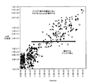
適切に最適化された酸窒化物は、純粋なSiO2に比べて、誘電率を高め、ゲート漏れ電流を下げ、そして拡散障壁特性を改善した。図1は、酸窒化物形成の遠隔プラズマ窒化(RPN)工程を使用するとき、処理時間の増加と共にゲート漏れ電流がどのように減少するかを示す。多くの場合、これらの改善は、トランジスタ・デバイス電流に影響を及ぼし得る移動度の変化に対して注意深く釣り合わせなければならない。さらに、この最適化は、同じ半導体チップ上にあるNFETデバイスとPFETデバイスで異なることがある。図1に、1.2ボルトでの(アンペア/cm2)単位のゲート漏れを、Tinv(Å)の関数として示す。パラメータTinvは反転厚さであり、反転厚さは、トランジスタが反転モードで測定されるとき、実効酸化物厚さの測定値(measure)である。単位は、オングストローム(Å)またはナノメートル(nm)のような厚さである。 Suitably optimized oxynitride, compared to pure SiO 2, increasing the dielectric constant, decreasing the gate leakage current, and improved diffusion barrier characteristics. FIG. 1 shows how gate leakage current decreases with increasing processing time when using a remote plasma nitridation (RPN) process of oxynitride formation. In many cases, these improvements must be carefully balanced against changes in mobility that can affect transistor device current. Furthermore, this optimization may be different for NFET and PFET devices on the same semiconductor chip. FIG. 1 shows gate leakage in units of (Amps / cm 2 ) at 1.2 volts as a function of T inv (Å). The parameter T inv is the inversion thickness, which is a measure of the effective oxide thickness when the transistor is measured in the inversion mode. The unit is a thickness such as angstrom (Å) or nanometer (nm).
図2〜5は、プラズマ窒化がPFETデバイスおよびNFETデバイスの駆動電流にどのように違った影響を及ぼすかの例を示す。これらの例は、ゲート誘電体中の最適窒素濃度はNFETデバイスとPFETデバイスで異なることを明らかにしているが、このことは一般に知られていない。縦軸はJoffであり、水平軸はJodlinであり、ここでJodlinは、トランジスタ・ドレイン電流密度(アンペア/μm)、すなわちソースとドレインの間のトランジスタの単位幅当たりのトランジスタ・ドレイン電流、を表す。任意の閾値電圧差を規準化するのを役立つのは、Vt(閾値電圧)より一定量上のVg(ゲート電圧)で測定されたトランジスタ電流である。Joffは、0ボルトがゲート電極に加えられている状態でのトランジスタの単位幅(ソースとドレインの間)当たりのオフ状態の漏れの測定値である。 Figures 2-5 show examples of how plasma nitridation affects the drive current of PFET and NFET devices differently. Although these examples demonstrate that the optimal nitrogen concentration in the gate dielectric is different for NFET and PFET devices, this is not generally known. The vertical axis is Joff and the horizontal axis is Jodlin, where Jodlin represents the transistor-drain current density (ampere / μm), that is, the transistor-drain current per unit width of the transistor between the source and drain. . Helping to normalize any threshold voltage difference is the transistor current measured at Vg (gate voltage) above a certain amount above Vt (threshold voltage). Joff is a measure of the off-state leakage per unit width (between source and drain) of the transistor with 0 volts applied to the gate electrode.
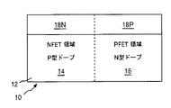
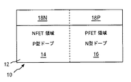
図6〜9は模式的な概念図であり、図6〜9は、図24の断面線A−A’に沿ったNFET領域14および関連した構造体(feature)、および図24の断面線B−B’に沿ったPFET領域16および関連した構造体の図である。図6〜9は、従来技術の工程の4つのステップでシリコン基板12に形成された半導体デバイス10の並置にされたPFET領域およびNFET領域を示し、これは、どのようにしてゲート誘電体の集積化の標準的な一連の処理ステップが、最も薄いゲート誘電体層を有する高性能トランジスタに、同じPFETおよびNFET酸窒化物ゲート誘電体層18N/18Pを生じさせるかを図示している。これは、薄いゲート誘電体層18N/18Pが成長されるとき、基板12のNFET領域14およびPFET領域16の両方が同じ工程にさらされるからである。工程が熱をベースあるいはプラズマをベースとしていてもこのことは言えることであるが、プラズマ工程を説明のために示す。
FIGS. 6-9 are schematic conceptual diagrams, FIGS. 6-9 show the NFET
図6において、デバイス10は、シリコン半導体基板12を備える、デバイス製造の初期段階が示されており、この基板12は、P型ドープ(P-doped)NFET領域14およびN型ドープ(N-doped)PFET領域16を基板12に含むように処理される。
In FIG. 6,
図7において、ゲート酸化物層18NがNFET領域14の上面の上に形成され、かつゲート酸化物層18PがPFET領域16の上面の上に形成された後の図6のデバイス10が示されている。
In FIG. 7, the
図8において、NFET領域14およびP型ドープPFET領域16の上面の上のゲート酸化物層18N/19P中に窒素を押し込むことによって、ゲート酸化物層18N/18Pが一様なプラズマ窒化で処理された後の図7のデバイス10が示されている。熱窒化について、同じことが言える。
In FIG. 8, the
図9において、図8のデバイス10は、同一ゲート誘電体層18Aがゲート酸化物層18Nおよび18Pの代わりにある状態で示されている。NFET領域14およびPFET領域16の上面の上の図8のゲート誘電体層18N/18Pの一様な窒化の結果として、ゲート酸化物層18N/18Pの同一ゲート誘電体層18Aへの変換を示すために、同一ゲート誘電体層18Aは水平の破線で陰影付けされている。図9は図24の線A−A’およびB−B’に沿った断面で構成されていることに留意すべきである。
In FIG. 9, the
最適酸窒化物はNFETデバイスとPFETデバイスで異なるので、この2つを個々に最適化することが非常に望ましい。その理由は、全体的なCMOS集積回路性能はNFETとPFETの両方のデバイス性能で決定されるからである。同じゲート誘電体層18N/18PがNFET領域14およびPFET領域16の上に同時に成長されると、一方のデバイスは最適化されるが、他方は半最適(sub-optimum)である。半最適デバイスがあるということは、製品の全体的なCMOS回路性能を制限することがある。
Since the optimal oxynitride is different for NFET and PFET devices, it is highly desirable to optimize the two individually. This is because the overall CMOS integrated circuit performance is determined by both NFET and PFET device performance. When the same gate
「Integrated Circuitry And SemiconductorProcessing Method of Forming Field Effect Transistors」という名称のTrivedi等の米国特許第6,093,661号は、デバイスのゲート誘電体層の任意の高さ位置で、好ましくはゲート誘電体層と単結晶シリコン半導体基板のPおよびN型ドープ領域との間の下の界面近くのゲート誘電体層中の位置で、ピークに達する窒素原子濃度を教示している。好ましくは、窒素原子濃度は、ゲート誘電体層中のピーク高さ(elevation)領域で0.1%から10.0%、好ましくは0.5%から5.0%であり、ピーク高さ領域の厚さは30Åから60Åである。ゲート誘電体層中への窒素の導入は、大気圧で、750℃から950℃理想的には850℃の温度の熱処理炉中で、窒素が約100から10,000sccm(0.169〜16.9Pa m3/s)理想的には1,000sccm(1.69Pa m3/s)で供給された状態で、5分から2時間理想的には30分、行うことができる。窒素原子の好ましい供給源は、窒素結合の破壊の容易さのために、N−O結合を有している。しかし、酸化窒素(NO)、一酸化二窒素(N2O)、アンモニア(NH3)、および窒素ガス(N2)のような他の供給源を使用することができる。そうでなければ、温度が毎秒約10℃から毎秒200℃の割合で上昇し10秒から2分の時間範囲でピークに達する速度で、大気圧で、約800℃から1200℃に加熱された反応炉中で、上述の窒素ベースの化合物の1つを使用して、急速熱処理(RTP:rapidthermal processing)で窒素原子をゲート誘電体層中に導入する。代わりに、窒素プラズマ処理または窒素イオン注入を使用して、窒素原子がゲート誘電体層に添加される。Trivedi等の目標は、少なくとも部分的に下の界面に沿ってSi−N結合を生成することである。下の界面領域についてのTrivedi等の好ましい目的は、PFETトランジスタ・ゲート層(ホウ素でP型ドープされる)からトランジスタ・チャネル中へのp型材料の後の外方拡散を防止することである。Trivedi等の他の目的は、半導体基板の後の処理中におけるゲート誘電体層のさらなる酸化を制限することである。Trivedi等は、ゲート誘電体層を再酸化するために窒素領域を形成した後で行われる半導体基板の随意のさらなる熱処理を述べている。そのような再酸化工程の例は、1,000sccm(1.69Pa m3/s)の純粋N2、6,000sccm(10.14Pa m3/s)のO2、50sccm(0.0845Pa m3/s)のN2中で900℃であり、塩素ソース・ガスを50sccm(0.0845Pa m3/s)で50分間使用する。関連特許に、「P-TypeFET in a CMOS with Nitrogen Atoms in the Gate Dielectric」という名称のTrivedi等の米国特許第6,417,546号、および「SemiconductorProcessing Method of Forming Field Effect Transistors」という名称のTrivedi等の米国特許第6,541,395号がある。 US Pat. No. 6,093,661 to Trivedi et al., Entitled “Integrated Circuitry And Semiconductor Processing Method of Forming Field Effect Transistors”, is located at any height of the gate dielectric layer of the device, preferably with the gate dielectric layer. It teaches the concentration of nitrogen atoms that reaches a peak at a location in the gate dielectric layer near the lower interface between the P and N-type doped regions of the single crystal silicon semiconductor substrate. Preferably, the nitrogen atom concentration is 0.1% to 10.0%, preferably 0.5% to 5.0% in the peak elevation region in the gate dielectric layer, and the peak height region The thickness is 30 to 60 mm. The introduction of nitrogen into the gate dielectric layer is performed at a pressure of about 100 to 10,000 sccm (0.169 to 16.sc.) in a heat treatment furnace at atmospheric pressure and a temperature of 750 to 950 ° C., ideally 850 ° C. 9 Pa m 3 / s) Ideally, 1,000 sccm (1.69 Pa m 3 / s) can be supplied for 5 to 2 hours, ideally 30 minutes. A preferred source of nitrogen atoms has an N—O bond for ease of breaking the nitrogen bond. However, other sources such as nitric oxide (NO), dinitrogen monoxide (N 2 O), ammonia (NH 3 ), and nitrogen gas (N 2 ) can be used. Otherwise, the reaction was heated from about 800 ° C. to 1200 ° C. at atmospheric pressure at a rate that increased at a rate of about 10 ° C. per second to 200 ° C. per second and peaked in a time range of 10 seconds to 2 minutes. In the furnace, nitrogen atoms are introduced into the gate dielectric layer by rapid thermal processing (RTP) using one of the nitrogen-based compounds described above. Instead, nitrogen atoms are added to the gate dielectric layer using nitrogen plasma treatment or nitrogen ion implantation. The goal of Trivedi et al. Is to create Si-N bonds at least partially along the lower interface. The preferred purpose of Tridi, et al. For the lower interface region is to prevent subsequent out-diffusion of p-type material from the PFET transistor gate layer (P-doped with boron) into the transistor channel. Another object, such as Trivedi, is to limit further oxidation of the gate dielectric layer during subsequent processing of the semiconductor substrate. Trivedi et al. Describe an optional further heat treatment of the semiconductor substrate that occurs after the formation of the nitrogen region to reoxidize the gate dielectric layer. An example of such a re-oxidation step is 1,000 sccm (1.69 Pam 3 / s) pure N 2 , 6,000 sccm (10.14 Pam 3 / s) O 2 , 50 sccm (0.0845 Pam 3). / S) at 900 ° C. in N 2 and using a chlorine source gas at 50 sccm (0.0845 Pa m 3 / s) for 50 minutes. Related patents include US Patent No. 6,417,546 such as “Travedi” named “P-TypeFET in a CMOS with Nitrogen Atoms in the Gate Dielectric”, and Tridi named “Semiconductor Processing Method of Forming Field Effect Transistors” U.S. Pat. No. 6,541,395.
「Method For Improved Plasma Nitridation ofUltra Thin Gate Dielectrics」という名称の、2002年9月19日に公開されたKhare等の米国公開特許第20020130377A1号は、「基板材料に初期酸窒化物層を形成して...集積回路デバイスのゲート誘電体を形成し、酸窒化物層は初期物理厚さを有する。次に、初期酸窒化物層は、プラズマ窒化にかけられ、プラズマ窒化は、最終物理厚さを有する最終酸窒化物層をもたらす。」と記載している。「窒素ドーピング、特に遠隔プラズマ窒化(RPN:remoteplasma nitridation)は、シリコン酸化物誘電体の誘電率(したがって、単位キャパシタンス)を増大させるための知られた技術である。ゲート酸化物層を窒化する知られた工程が説明される。」と述べている。さらに、「シリコン基板は...酸素添加環境中で...基板を加熱することのような酸化にかけられ、それによって、...SiO2の...絶縁性酸化物層を形成し、...酸化物層の誘電体性能は、...ゲート厚さがディープ・サブミクロン寸法に縮小するときに、ますます重要になる。酸化物層の誘電率を改善して...単位キャパシタンス当たりのより小さな漏れ電流を実現するために、遠隔プラズマ窒化(RPN)として知られている工程によって、励起窒素原子が酸化物層に導入され...。RPN工程の結果として、酸化物層は...一般的な化学組成SiOxNyを有する...シリコン酸窒化物層に変換される。...」と述べている。 US Patent No. 200201330377A1 of Khare et al., Published on September 19, 2002, named “Method For Improved Plasma Nitridation of Ultra Thin Gate Dielectrics”, stated, “By forming an initial oxynitride layer on a substrate material. ... forming the gate dielectric of the integrated circuit device, the oxynitride layer having an initial physical thickness, which is then subjected to plasma nitridation, the plasma nitridation having a final physical thickness Resulting in a final oxynitride layer. " “Nitrogen doping, particularly remote plasma nitridation (RPN), is a known technique for increasing the dielectric constant (and hence unit capacitance) of silicon oxide dielectrics. Knowledge of nitriding gate oxide layers The steps taken are explained. " In addition, “The silicon substrate ... is subjected to oxidation, such as heating the substrate ... in an oxygenated environment, thereby forming an insulating oxide layer of ... SiO 2 . The dielectric performance of the oxide layer becomes increasingly important when the gate thickness is reduced to deep sub-micron dimensions, improving the dielectric constant of the oxide layer ... unit In order to achieve a smaller leakage current per capacitance, excited nitrogen atoms are introduced into the oxide layer by a process known as remote plasma nitridation (RPN) ... As a result of the RPN process, the oxide layer Is converted into a silicon oxynitride layer having a general chemical composition SiOxNy ... ".
RPN工程は、温度敏感材料を使用するとき問題を引き起こす高温工程である。 The RPN process is a high temperature process that causes problems when using temperature sensitive materials.
「SOI Device With Reduced JunctionCapacitance」という名称の、2002年12月12日に公開されたFurukawaの米国公開特許第20020185675A1号は、「熱酸化の後に続く遠隔プラズマ窒化(RPN)またはデカップルド(分離)プラズマ窒化(DPN:decoupledplasma nitridation)による酸化物の窒化によって形成されたシリコン酸窒化物である」ゲート誘電体の形成の例を記載している。 Furukawa's US Published Patent No. 20020185675A1, published December 12, 2002, entitled “SOI Device With Reduced Junction Capacitance”, “Remote Plasma Nitriding (RPN) or Decoupled (Separated) Plasma Nitriding Following Thermal Oxidation. An example of the formation of a gate dielectric is described, which is a silicon oxynitride formed by nitriding of an oxide (DPN: decoupled plasma nitridation).
「Method for Fabricating SemiconductorDevices Having Dual Gate Oxide Layers」という名称の、2003年5月29日に公開されたLim等の米国公開特許第20030100155A1号は、「a)半導体基板にゲート酸化物層を形成するステップ、およびb)デカップルド・プラズマ処理を行うことによってゲート酸化物層の一部の厚さを増加させるステップを含んだ二重ゲート酸化物を形成する方法」を備える選択DPN「分離処理」工程を記載している。さらに、「二重ゲート酸化物層はデカップルド・プラズマで形成されるので、追加の熱工程は必要でない。また、シリコン基板は損傷を受けないので、半導体デバイスのチャネル特性を保証することができる。さらに、追加のチャネル・イオン注入なしに、セル領域の閾値電圧は高められるので、半導体デバイスの電気特性を高めることができる。」と記載している。DPN処理は、「セル領域I」に使用されるが、「周辺回路領域II」では使用されない。セル領域Iおよび周辺回路領域IIは区別されるが、Lim等は、CMOSNFET領域およびPFET領域を区別するという概念を考えていない。Lim等は、チップのセル領域対周辺領域で異なったゲート誘電体厚さを生成する方法を開示し、この方法は、それぞれの領域の各々の中のNFETおよびPFETに同じゲート誘電体を生成するが、本発明の方法は、NFETとPFET(これらは、同じ厚さを有するようになる)を分離する。単一チップの複数のゲート誘電体厚さは、当産業ではまったく一般的なことである。例えば、単一チップに15Å、30Å、70Åのゲート誘電体があるかもしれない。しかし、各誘電体厚さの範囲内で、ゲート誘電体組成および厚さは、NFETおよびPFETの誘電体層で同じであり、このことが業界標準である。 US Pat. No. 20030100155A1, Lim et al., Published May 29, 2003, entitled “Method for Fabricating Semiconductor Devices Having Dual Gate Oxide Layers”, describes a step of forming a gate oxide layer on a semiconductor substrate. A selective DPN “separation process” step comprising “a method of forming a double gate oxide comprising the steps of increasing the thickness of a portion of the gate oxide layer by performing a decoupled plasma process”; doing. Furthermore, “the double gate oxide layer is formed by decoupled plasma, so no additional thermal process is required. Also, since the silicon substrate is not damaged, the channel characteristics of the semiconductor device can be guaranteed. Furthermore, the electrical characteristics of the semiconductor device can be improved because the threshold voltage of the cell region can be increased without additional channel ion implantation. " The DPN process is used for the “cell region I”, but is not used for the “peripheral circuit region II”. Although the cell region I and the peripheral circuit region II are distinguished, Lim et al. Does not consider the concept of distinguishing the CMOS NFET region and the PFET region. Lim et al. Disclose a method of generating different gate dielectric thicknesses in the chip cell region versus the peripheral region, which method generates the same gate dielectric for the NFET and PFET in each of the respective regions. However, the method of the present invention separates the NFET and the PFET, which will have the same thickness. Multiple gate dielectric thicknesses on a single chip are quite common in the industry. For example, a single chip may have 15Å, 30Å, and 70Å gate dielectrics. However, within each dielectric thickness range, the gate dielectric composition and thickness are the same for NFET and PFET dielectric layers, which is industry standard.
DPN工程は低温工程であり、温度敏感材料を使用するときの問題を防止する。 The DPN process is a low temperature process and prevents problems when using temperature sensitive materials.
Trivedi特許‘395号において、窒素(N)は、ホウ素浸透の低減のためにPFETゲート誘電体層に加えられ、窒素(N)はNFETゲート誘電体層に加えられない。ゲート誘電体層の電気特性は、5〜20Å(本発明の好ましい範囲)と30〜50Å(Trivedi等の好ましい範囲)とでは非常に異なる。窒素濃度の増加による漏れ減少は、一般に、シリコン酸化物が約20Åよりも下のときだけ観察される。Trivedi等の特許は、本発明よりも遥かに厚い酸化物を対象にしているようである。Trivedi等がNをPFETのゲート酸化物中に入れる理由は、ゲート酸化物にNを加えることで酸窒化物を形成することであり、酸窒化物はホウ素拡散を阻止する傾向がある。そのことは、P+ポリシリコン・ゲート電極からPFETのチャネル中へのホウ素浸透を減少させるという利点を有する。20Å以下の厚さ範囲では、NFETデバイスとPFETデバイスの両方で、純粋SiO2に比べて、酸窒化物によってゲート漏れ(leakage)が減少する。したがって、本発明は、NFETとPFETの両方のゲート誘電体層にNを入れる。
Trivedi等の特許は、最初に窒化シリコン酸化物の成長、レジスト・マスキングとHFエッチング、それから第2の(窒素がない)シリコン酸化物の成長を使用する。最初のシリコン酸化物は、第2の(窒素がない)酸化物にさらされるので、常により厚い。Trivedi等の特許は、比較的高温の熱工程に関するので、そこに記載された工程は、常に、結果として比較的厚い第2のシリコン酸化物(PFET用のより薄い酸窒化物およびNFET用のより厚いSiO2)を生じさせる。NFETのより厚い酸化物は、トランジスタ駆動電流を減少させるマイナスの効果を有する。本発明は、Trivedi等の特許によって開示されたような高温酸化で見られる物理厚さの増加をなくすることができる低温プラズマを使用して、酸化物を生成する手段を提供する。したがって、本発明は、CMOSデバイスの2つの異なる領域、すなわちNFETゲート誘電体層とPFETゲート誘電体層に、異なるレベルの窒素濃度を実現しながら、NFETとPFETの両方のゲート誘電体層に同じ物理厚さを実現することができる(物理厚さの増加がトランジスタ電流を減少させるということで生じるトランジスタ電流減少の問題を起こさないようにする)。 The Trivedi et al. Patent uses silicon nitride oxide growth first, resist masking and HF etching, and then a second (no nitrogen) silicon oxide growth. The first silicon oxide is always thicker because it is exposed to the second (no nitrogen) oxide. Because the Trivedi et al. Patent relates to a relatively high temperature thermal process, the process described therein always results in a relatively thick second silicon oxide (thinner oxynitride for PFETs and more for NFETs). Thick SiO 2 ). The thicker oxide of the NFET has the negative effect of reducing the transistor drive current. The present invention provides a means for producing oxides using a low temperature plasma that can eliminate the physical thickness increase seen with high temperature oxidation as disclosed by the Trivedi et al. Patent. Thus, the present invention is the same for both NFET and PFET gate dielectric layers while achieving different levels of nitrogen concentration in two different regions of the CMOS device, namely the NFET gate dielectric layer and the PFET gate dielectric layer. Physical thickness can be realized (so that the increase in physical thickness does not cause the problem of transistor current reduction caused by reducing transistor current).
Lim等を参照して、第1の非常に重要な差は、NFETゲート誘電体層の最適組成がPFETゲート誘電体層の最適組成と異なっているという我々の発見に本発明が基づいていることである。このことは一般に知られておらず、多くの実験を通して初めて我々はそれを発見した。第2に、上述の事実を知るとすぐに、CMOS性能を完全に最適化するために異なる酸窒化物濃度のNFETおよびPFETゲート誘電体層を生成することが非常に望ましいことに、我々は気付いた。本発明は、この向上した結果を実現するために、ソフト・フォトレジスト・マスクの組合せと共にDPNのような低温工程の使用を採用する。 Referring to Lim et al., The first very important difference is that the present invention is based on our discovery that the optimum composition of the NFET gate dielectric layer is different from the optimum composition of the PFET gate dielectric layer. It is. This is not generally known and for the first time through many experiments we discovered it. Second, as soon as we know the above facts, we realize that it is highly desirable to produce NFET and PFET gate dielectric layers with different oxynitride concentrations to fully optimize CMOS performance. It was. The present invention employs the use of a low temperature process such as DPN along with a soft photoresist mask combination to achieve this improved result.
本発明の顕著な特徴は次の通りである。
室温プラズマによって、窒化で処理される領域のパターン形成においてフォトレジスト・ソフトマスクを使用することが可能になる。
PFET領域とNFET領域の両方に窒素が導入される(他の領域には、強い窒化にさらされたキャパシタ誘電体層を有する減結合(decoupling)キャパシタを含み得る)。
NFETの窒素は、ゲート漏れの減少に有利であるが、N濃度が余りにも高いとき移動度を劣化させる。
PFETの窒素は、ゲート漏れ/ホウ素浸透を減少させ、移動度を改善する。前の2つの事実(一般に知られていない)を組み合わせることで、PFETおよびNFETのゲート酸化物を個々に最適化しようと導かれる。
The salient features of the present invention are as follows.
The room temperature plasma makes it possible to use a photoresist soft mask in patterning regions that are treated with nitridation.
Nitrogen is introduced into both the PFET region and the NFET region (other regions may include decoupling capacitors having capacitor dielectric layers exposed to strong nitridation).
NFET nitrogen is beneficial in reducing gate leakage, but degrades mobility when the N concentration is too high.
PFET nitrogen reduces gate leakage / boron penetration and improves mobility. Combining the previous two facts (which are not generally known) leads to individual optimization of the PFET and NFET gate oxides.
同じ基礎酸化物がNFET領域とPFET領域の両方に使用され、窒素は個々に最適化される。サンプル:NFET用の領域Nドーズ量=0.8E15から1.2E15cm−2、PFET用のNドーズ量=1.5E15から2.5E15cm−2。この構成は、用途および所望の結果に依存して逆にすることができる。これは、単に、我々の発明に従った製造方法およびこの方法の製品に特に有利でかつ好ましいと分かった例に過ぎない。 The same base oxide is used for both the NFET region and the PFET region, and nitrogen is optimized individually. Sample: Region N dose for NFET = 0.8E15 to 1.2E15 cm −2 , N dose for PFET = 1.5E15 to 2.5E15 cm −2 . This configuration can be reversed depending on the application and the desired result. This is merely an example that has proved particularly advantageous and preferred for the manufacturing method according to our invention and the products of this method.
本発明の前述およびその他の態様および有利な点は、添付の図面を参照して以下で説明し、また記述する。 The foregoing and other aspects and advantages of the invention are described and described below with reference to the accompanying drawings.
A)NFETデバイスおよびPFETデバイスの酸窒化物ゲート誘電体の最適化は、デバイスごとに異なる。
B)最適酸窒化物組成はNFETデバイスとPFETデバイスで異なるので、NFETデバイスおよびPFETデバイスのために酸窒化物組成を個々に最適化することが、全体的なCMOS性能(NFETとPFETの組合せ)にとって有利である。
C)本発明の方法は、単一半導体チップ内のNFETデバイスとPFETデバイスのゲート酸窒化物の個々の最適化を実現するのに適応している。
A) Optimization of oxynitride gate dielectrics for NFET and PFET devices varies from device to device.
B) Since the optimal oxynitride composition is different for NFET and PFET devices, optimizing the oxynitride composition individually for NFET and PFET devices is the overall CMOS performance (combination of NFET and PFET) Is advantageous to.
C) The method of the invention is adapted to achieve individual optimization of the gate oxynitride of NFET and PFET devices in a single semiconductor chip.
前に説明したように、NFETデバイスとPFETデバイスの両方の全体的な性能を最適化することができるように、NFETデバイスおよびPFETデバイスのゲート誘電体層18N/18Pの個々の最適化を行うことが望ましい。本発明のいくつかの実施形態を以下で説明する。
As previously described, performing individual optimization of the
図10〜15の実施形態において、基板12のP型ドープNFET領域14の上の低濃度窒化(lightly nitrided)NFETゲート誘電体層18CおよびN型ドープPFET領域16の上のより高濃度窒化(heavilynitrided)PFETゲート誘電体層18Bの形成工程は、2つの別個のリソグラフィ・マスキング・ステップを使用して完全に分離されている。図10〜15において、同様な要素には、図6〜9に示した要素と同様な参照数字がついている。
In the embodiment of FIGS. 10-15, lightly nitrided NFET
図10は、製造の初期段階における、本発明にしたがって製造されるデバイス10を示す。デバイス10は、シリコン半導体基板12を含み、この基板12は、P型ドープNFET領域14とN型ドープPFET領域16の両方を基板12に含むように処理されている。
FIG. 10 shows a
図11の工程ステップ
(1aa)図11は、NFET領域14およびPFET領域16の上にゲート酸化物層18N/18Pをそれぞれ形成した後(図12に示すようにレジスト・マスクPR1を形成する前)の図10のデバイス10を示す。ゲート酸化物層18N/18Pを形成するために、好ましくは、薄い基礎(base)ゲート酸化物層18N/18P(SiO2またはSiOxNy)を成長する次のステップが行われた。
Process Steps of FIG. 11 (1aa) FIG. 11 shows that after forming the
望ましい膜特性
薄い基礎ゲート酸化物層18N/18Pの物理厚さの望ましい範囲は、5Å〜100Åの範囲内であり、この好ましい厚さは特定の用途に依存している。窒素の取込みによるゲート漏れ減少のために好ましい厚さは5Å〜20Åである。
Desirable Film Properties The desired range of physical thickness of the thin base
組成は、シリコン酸化物(SiO2)から0%〜30%の範囲の窒素のパーセンテージ(N%)を有するあるレベルの酸窒化物に及び、好ましい範囲は3〜10%である。 The composition ranges from silicon oxide (SiO 2 ) to some level of oxynitride with a percentage of nitrogen (N%) ranging from 0% to 30%, with a preferred range of 3-10%.
炉(バッチ工程)
ガス:O2、NO、N2O、NH3または組合せ
温度範囲:600℃〜1000℃、700℃〜850℃が好ましい
圧力:10トル〜760トル(1330Pa〜101080Pa)
時間は5分から3時間であるが、好ましくは20〜60分、
または、(1aa)の代わりとして、以下で(1ab)のステップを行う。
Furnace (batch process)
Gas: O 2 , NO, N 2 O, NH 3 or combination Temperature range: 600 ° C. to 1000 ° C., preferably 700 ° C. to 850 ° C. Pressure: 10 torr to 760 torr (1330 Pa to 101080 Pa)
The time is from 5 minutes to 3 hours, preferably 20-60 minutes,
Alternatively, instead of (1aa), the following step (1ab) is performed.
(1ab)単一ウェハ急速加熱処理装置(RTP)
ガス:O2、NO、N2O、NH3または組合せ
温度範囲:700℃〜1100℃、800℃〜950℃が好ましい
圧力:10トル〜760トル(1330Pa〜101080Pa)
時間は5秒から400秒であるが、好ましくは15〜30秒。
(1ab) Single wafer rapid thermal processing equipment (RTP)
Gas: O 2 , NO, N 2 O, NH 3 or combination Temperature range: 700 ° C. to 1100 ° C., preferably 800 ° C. to 950 ° C. Pressure: 10 torr to 760 torr (1330 Pa to 101080 Pa)
The time is 5 seconds to 400 seconds, but preferably 15 to 30 seconds.
第1のフォトリソグラフィ・ステップ−PFETまたはNFETのゲート酸化物層を遮蔽するマスクを形成:
(1b)図12(図8の修正である)は、ゲート酸化物領域18Nを覆うがPFET領域16の上のゲート酸化物18Pを露出させるように、標準的な遮蔽フォトレジスト(レジスト)・マスクPR1を形成する工程の第2のステップを行った後の図11のデバイス10を示す。言い換えると、マスクPR1は、NFET領域14の上の酸化物を覆うが、PFET領域16の上の酸化物18Pを露出させる。すなわち、遮蔽レジスト・マスクPR1は、NFET領域14の上のゲート酸化物層18Nを覆い、PFET領域16の上のゲート酸化物18Pの部分を露出されたままにしておく。
First photolithography step—form a mask to shield the gate oxide layer of the PFET or NFET:
(1b) FIG. 12 (a modification of FIG. 8) shows a standard shielding photoresist (resist) mask that covers the
第1のゲート酸化物領域の窒化
(1c)図12は、また、ウェハ表面が露出されているPFET領域16の上の図11のゲート酸化物層18Pの、窒素含有プラズマ19Pによるプラズマ窒化の窒化中における図11のデバイス10を示す。他方で、レジスト・マスク層PR1は窒素プラズマ19PがNFET領域14の上の酸化物表面18Nに到達するのを妨げるので、プラズマ19Pは、NFET領域14の上のゲート酸化物層18Nの窒化を生じさせない。ステップ(1c)の処理パラメータは、次に説明する。
Nitridation of the first gate oxide region (1c) FIG. 12 also shows the nitridation of the plasma nitridation by the nitrogen-containing
最初に低温プラズマ窒化を行う(フォトレジストPR1を保護するために、高温工程を使用できない)。 First, low temperature plasma nitridation is performed (a high temperature process cannot be used to protect the photoresist PR1).
望ましい膜特性
物理厚さ5Å〜100Å、好ましい厚さは特定の用途に依存する。酸窒化物組成は、特定の用途に依存して、1〜30%のN%の範囲にあり、5〜15%が好ましい。
Desirable film properties
低温プラズマ窒化
プラズマ源:標準プラズマ発生器、しかし、好ましくは、RF(高周波)
窒素供給源ガス:好ましくはN2、しかし、NO、N2O、NH3が可能
キャリア・ガス:好ましくはHeまたはAr、しかしKrも可能
温度:15℃〜100℃、好ましくは25℃
圧力:1ミリトルから1トル(0.133Pa〜133Pa)、好ましくは10ミリトルから200ミリトル(1.33Pa〜26.6Pa)
50Wから1000Wのパワー、しかし、好ましくは100Wから200W
時間は5〜400秒、しかし、好ましくは15〜30秒
Low temperature plasma nitridation Plasma source: Standard plasma generator, but preferably RF (radio frequency)
Nitrogen source gas: preferably N2, however, NO, N 2 O, NH 3 can carrier gas: preferably He or Ar, but Kr possible Temperature: 15 ° C. to 100 ° C., preferably 25 ° C.
Pressure: 1 millitorr to 1 torr (0.133 Pa to 133 Pa), preferably 10 millitorr to 200 millitorr (1.33 Pa to 26.6 Pa)
50W to 1000W power, but preferably 100W to 200W
Time is 5 to 400 seconds, but preferably 15 to 30 seconds
(1d)図12の工程の結果が図13に示され、ここで、ゲート酸化物層18Pは、上述した上のステップ(1c)で窒化されてゲート誘電体層18Bに変換され、水平破線で陰影付けされたゲート誘電体層18BはN型ドープPFET領域16の上面の上のゲート酸化物層18の比較的高濃度窒化によるゲート誘電体領域18Bの形成を示しており、一方で、ゲート酸化物層18Nは、図11の終りの以前の状態のままで残っている。言い換えると、マスクPR1を通して露出されている(例えば、PFET)SiO2領域18Bは、プラズマ19Pによって窒化されたが、一方で、レジスト・マスクPR1で覆われた(例えば、NFET)層18Nは窒化から保護された。
(1d) The result of the process of FIG. 12 is shown in FIG. 13, where the
第1のマスクを剥離
図13は、また、レジスト・マスクPR1が標準的なフォトレジスト剥離でデバイス10から剥離された後の図12のデバイス10を示す。
Stripping the first mask FIG. 13 also shows the
第2のフォトリソグラフィ・ステップ−NFETまたはPFETのゲート酸化物層を遮蔽するマスクを形成
(1e)図14は、今度は反対側の領域を覆って(例えば、PFETゲート誘電体層18Bを覆い、NFETゲート酸化物層18Nを露出させる)、ゲート誘電体領域18Bの上に遮蔽レジスト・マスクPR2を形成し、残りのNFETゲート酸化物領域18NをNFET領域14の上に露出されたままするように、第2のフォトリソグラフィ・ステップを行った後の図13のデバイス10を示す。
Second Photolithographic Step—Forming Mask to Shield NFET or PFET Gate Oxide Layer (1e) FIG. 14 now covers the opposite area (eg, PFET
第2のプラズマ窒化
(1f)再び図14を参照して、次のステップは、別のプラズマ窒化(プラズマ19Nを含んだ窒素がNFET領域14の上のNFETゲート酸化物層18Nの窒化を行って、それをゲート誘電体層18C(図15)に変換する第2のプラズマ窒化)を行うことであるが、工程中のこのステップは、遮蔽レジスト・マスクPR2のために、PFETゲート誘電体層18Bの窒化を行わない。
Second plasma nitridation (1f) Referring again to FIG. 14, the next step is to perform another plasma nitridation (
図15は、デバイス10のNFET/PFET領域14/16のNFETゲート誘電体層18CおよびPFETゲート誘電体層18Bのために、窒素濃度および工程を個々に最適化することができるように、デバイス10のNFET領域およびPFET領域を完全に分離する上述のシーケンスを使用した後の図14のデバイス10を示す。
FIG. 15 illustrates the
2つのマスキング・ステップ(PR1/PR2)があり、順序は逆にすることができるので、高濃度窒化か低濃度窒化かどちらでも最初に行うことができる。 Since there are two masking steps (PR1 / PR2) and the order can be reversed, either high or low concentration nitridation can be performed first.
所望の膜特性
物理厚さ5Å〜100Åの好ましい厚さは、特定の用途に依存し、ゲート漏れ電流減少が望ましい場合には、5Å〜20Åが望ましい。
酸窒化物組成は、特定の用途に依存して、1〜30%のN%の範囲にあり、5〜15%が好ましい。
Desired film properties The preferred thickness of 5 to 100 mm of physical thickness depends on the particular application, and 5 to 20 mm is desirable if gate leakage current reduction is desired.
Depending on the specific application, the oxynitride composition is in the range of 1-30% N%, preferably 5-15%.
低温プラズマ窒化
プラズマ源:標準プラズマ発生器、しかし、好ましくは、RF(高周波)
窒素供給源ガス:好ましくはN2、しかし、NO、N2O、NH3が可能
キャリア・ガス:好ましくはHeまたはAr、しかしKrも可能
温度:15℃〜100℃、好ましくは25℃
圧力:1ミリトルから1トル(0.133Pa〜133Pa)、好ましくは10ミリトルから200ミリトル(1.33Pa〜26.6Pa)
50Wから1000Wのパワー、しかし、好ましくは100から200W
時間は5〜400秒、しかし、好ましくは15〜30秒。
Low temperature plasma nitridation Plasma source: Standard plasma generator, but preferably RF (radio frequency)
Nitrogen source gas: preferably N 2, however, NO, N 2 O, NH 3 can carrier gas: preferably He or Ar, but Kr possible Temperature: 15 ° C. to 100 ° C., preferably 25 ° C.
Pressure: 1 millitorr to 1 torr (0.133 Pa to 133 Pa), preferably 10 millitorr to 200 millitorr (1.33 Pa to 26.6 Pa)
50W to 1000W power, but preferably 100 to 200W
The time is 5 to 400 seconds, but preferably 15 to 30 seconds.
この特定の例では、PFET領域への最初のプラズマ窒化19Pの、ゲート酸化物層で表された工程条件は、ゲート酸化物層で表されたNFET工程19Nよりも多くの窒素を導入するようなものである。ゲート酸化物層の窒化19Pの工程のより高い窒素濃度は、より長い時間、より高いパワー、またはより低い圧力のような様々なパラメータによって実現することができる。
In this particular example, the process conditions represented by the gate oxide layer of the
第2のマスクを剥離
(1g)図15に示すようにマスクPR2を除去するレジスト剥離工程を行う。ここで、ゲート誘電体層18Cは、上で説明したように以前により高濃度窒化されたN型ドープPFET領域16の上でなく、P型ドープNFET領域14の上面の上の低濃度窒化されたゲート酸化物層18Nのゲート誘電体領域18Cの窒化の結果を示すように点(ドット)で薄く陰影付けされた。
Strip the second mask (1g) As shown in FIG. 15, a resist stripping process is performed to remove the mask PR2. Here, the
(1h)トランジスタを形成するための通常の工程流れを続ける。例えば、図26で示すようにポリシリコン・ゲート堆積を行う。 (1h) Continue the normal process flow for forming transistors. For example, polysilicon gate deposition is performed as shown in FIG.
以下に見出される第2および第3の実施形態の説明は、基礎(ベース)酸化物およびプラズマ窒化の範囲は第1の実施形態と変わらないので、これらの比較的詳細でない説明を含む。 The descriptions of the second and third embodiments found below include these relatively non-detailed descriptions since the scope of the base (base) oxide and plasma nitridation is the same as the first embodiment.
図16〜19を参照して説明するこの方法の場合には、図10〜15で示すような第1の実施形態の二重マスキング・ステップとは対照的に、単一リソグラフィ・マスキング・ステップを使用して、図19に示すようにNFETおよびPFETの誘電体領域18Dと18Eが分離されている。
In the case of this method described with reference to FIGS. 16-19, in contrast to the double masking step of the first embodiment as shown in FIGS. In use, the NFET and PFET
(2a)図16を参照すると、第1の実施形態のステップ(1aa)またはステップ(1ab)を参照して上で説明したように、薄い基礎ゲート酸化物層18N/18P(SiO2またはSiOxNy)が成長されている。
(2a) Referring to FIG. 16, a thin base
(2b)NFETゲート酸化物18Nである左部分を覆うフォトレジスト・マスクPR3を使用し、ここで、図19のゲート誘電体デバイス領域18Dはより低濃度に窒化されるようになる(例えば、NFET領域14の上のゲート酸化物層18Nを覆い、PFET領域16の上のゲート酸化物層18Pを露出させる)。
(2b) Using a photoresist mask PR3 covering the left portion of the
(2c)図16を参照すると、図19のより高濃度に窒化されたゲート誘電体18EがPFET領域16の上に形成されるために必要な窒素濃度の大部分および工程を含む、プラズマ19Pによるマスクされた第1のプラズマ窒化が行われる。工程の詳細については上記を参照されたい。
(2c) Referring to FIG. 16, by
(2d)レジスト・マスクPR3を剥離する。図17は、マスクPR3を除去した後の図16のデバイス10を示し、さらにゲート酸化物層18PがPFET領域16の上で高濃度に窒化されたゲート誘電体層18Bを示す。
(2d) The resist mask PR3 is removed. FIG. 17 shows the
(2e)図18を参照すると、ゲート酸化物層18Nと部分的に窒化されたPFETゲート誘電体層18Bの両方の中に窒化物に導入するように、プラズマ19N’による追加(第2)のより低濃度のプラズマ窒化が行われる。このマスクされない第2のプラズマ窒化は、図19に示すように、すでに低濃度に窒化されている窒化ゲート誘電体層18B中の窒素濃度を高めて、PFETゲート誘電体層18Eを最適化しかつNFET領域14の上にNFETゲート誘電体層18Dを実現するのに必要なレベルに達する高濃度ドープPFETゲート誘電体層18Eを形成する。
(2e) Referring to FIG. 18, an additional (second)
もしくは、最初にマスクなしでより低濃度の窒化を行い、それから、NFETゲート誘電体層18Dがマスクされている状態で、第2の窒化を行うことができる。
Alternatively, a lower nitridation can be performed without a mask first, and then a second nitridation can be performed with the NFET
(2f)トランジスタを形成するために工程流れの残りを続ける(例えば、ポリシリコン堆積)。 (2f) Continue the rest of the process flow to form transistors (eg, polysilicon deposition).
このシーケンスを使用することで、デバイス10のNFET領域とPFET領域は分離されるが、より高濃度に窒化されたNFETゲート誘電体層18Eの窒素濃度は2つの窒化ステップの和であるので、完全とは言えない。このシーケンスは、第1の実施形態に比べてマスキング・ステップを節約する。
Using this sequence, the NFET and PFET regions of
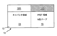
図20から23は、PFET領域16(またはNFET領域14、説明の便宜上PFET領域16だけを示す)であり得る領域の窒化と組み合わせて、キャパシタ領域24の上のキャパシタ誘電体層18F(図9で示すように)に有用な高濃度窒化シリコン酸化物のための窒化を実現する工程を示す。キャパシタ誘電体層の望ましい特性は、単位面積当たりの高いキャパシタンス、低い漏れ、および高信頼性である。キャパシタは、トランジスタ伝導電流がないので、高移動度を必要としない。したがって、キャパシタが洩れ難くなり、かつ単位面積当たりにより高い容量密度を有するようになるように、膜の誘電率を最適化するのに必要なだけの窒素を添加することが望ましい。
20-23 are combined with a nitridation of a region that can be a PFET region 16 (or
工程シーケンスは次の通りである。 The process sequence is as follows.
3a)上記で説明した実施形態のように、トランジスタ用の基礎酸化物18P/18N(NFET領域およびPFET領域14/16)およびキャパシタ領域24の基礎酸化物18Kを成長する。これらの基礎酸化物18Kおよび18P/18Nは、必要であれば、異なる酸化物厚さを有することができ、図20および21で示すように標準的な酸化および集積化シーケンスによって生成される。ここで、マスクPR5で保護された左のキャパシタ領域24の上のシリコン酸化物層18Kの上にマスクPR5がある状態で、プラズマ19Pを用いたPFET領域16の上の窒化は、窒化ゲート誘電体18B(PFET領域16の上)を実現している。したがって、シリコン酸化物層18Kは、この点で窒化のない状態のままになっている。
3a) Growing the
3b)次に、図22で示すように、トランジスタ領域の窒化ゲート誘電体層18B、その他をマスクPR6で覆うように、フォトリソグラフィ・マスキング・ステップが図21のデバイスに対して行われる。保護された領域には、PFET領域16のゲート誘電体層18BおよびNFET領域14のゲート誘電体層18C(この図には示されていない)がある。マスクPR6は、酸化シリコン層18Kがキャパシタ領域24の上に露出されたままにする。
3b) Next, as shown in FIG. 22, a photolithographic masking step is performed on the device of FIG. 21 to cover the nitrided
3c)図23は、図22の開口したキャパシタ領域をプラズマ19N’にさらした後の図22のデバイス10を示し、このプラズマ19N’は、図23のキャパシタ誘電体層18Fを適切な窒素濃度に窒化する。移動度は問題でなく、漏れとキャパシタンスだけが最適化されればよいので、一般に、この濃度は、トランジスタ(NFETおよびPFET)領域よりも高濃度である。
3c) FIG. 23 shows the
NFETデバイスまたはPFETデバイスのような様々なデバイス領域で選択的最適化プラズマ窒化を必要とするか、または選択的最適化プラズマ窒化から恩恵を受ける、どんな高Kゲート誘電体(HfO2、HfSiO2、ZrO2、その他)の集積化にも、これらの実施形態のどれでも応用することができる。 Any high-K gate dielectric (HfO 2 , HfSiO 2 , HfO 2 , HfSiO 2 , that requires or benefits from selective optimized plasma nitridation in various device regions such as NFET or PFET devices Any of these embodiments can also be applied to the integration of ZrO 2 , etc.).
図24(a)は、本発明および従来技術に従ったインバータ回路(図示のように接続されたNFETおよびPFETデバイス)の平面図を示す。 FIG. 24 (a) shows a plan view of an inverter circuit (NFET and PFET devices connected as shown) according to the present invention and the prior art.
図24(b)は、図24の陰影付け部分の凡例を示す。 FIG. 24B shows a legend of the shaded portion of FIG.
図24(c)は、図24のデバイスの概略回路図である。 FIG. 24C is a schematic circuit diagram of the device of FIG.
図24(a)を参照すると、そのような回路(インバータはすべてのCMOS回路の構成要素である)のデバイスのゲート酸化物の組成を調べることによって、当業者にはよく知られている分析技術を使用してNFET領域14の上のゲート誘電体層の窒素濃度がPFET領域16の上のゲート誘電体層の窒素濃度と同じであるかどうかを容易に決定することができる。
Referring to FIG. 24 (a), analytical techniques well known to those skilled in the art by examining the gate oxide composition of devices in such circuits (inverters are components of all CMOS circuits). Can be used to easily determine whether the nitrogen concentration of the gate dielectric layer above the
標準のゲート誘電体集積化シーケンスは、結果として、NFET領域およびPFET領域に同じ窒素濃度を生じさせる。 A standard gate dielectric integration sequence results in the same nitrogen concentration in the NFET and PFET regions.
本発明は、NFETおよびPFETのゲート誘電体層のゲート誘電体に異なる窒素濃度を与え、このことは有利であり、また本発明はそのような構成を実現する方法を提供する。 The present invention provides different nitrogen concentrations to the gate dielectrics of the NFET and PFET gate dielectric layers, which is advantageous, and the present invention provides a way to implement such a configuration.
図25は、NFET領域14およびPFET領域16の各々のゲート誘電体層18Aの上にゲート電極30/32を形成し、それに続いてデバイス10のNFET領域14およびPFET領域16の各々に自己整合ソース領域Sおよびドレイン領域Dを形成した後の、Khare等の公開特許出願の教示に似ている図9のデバイス10を示す。Khare等の公開出願によって教示された内容の重要な特徴は、ゲート誘電体厚さおよび窒素濃度はNFETとPFETの両方のデバイス領域で同じであり、したがって2つのデバイスのうちの一方にとっては最適でないということである。
FIG. 25 illustrates the formation of a gate electrode 30/32 over the
図26は、NFET領域14のNFETゲート誘電体層18Dの上のゲート電極40およびPFET領域16を覆うPFETゲート誘電体層18Eの上のゲート電極42を形成し、それに続いて、デバイス10のNFET領域14およびPFET領域16の各々に自己整合ソース領域Sおよびドレイン領域Dを形成した後の、本発明に従った図19のデバイスを示す。ゲート誘電体厚さは両方の領域で実質的に同じであるが、物理厚さが異なっている米国特許第6,541,395号のTrivediのデバイスと対照的に、窒素濃度は、NFETとPFETとで異なっている。
26 forms a
図27は、CMOS集積回路を共に形成するNFETデバイスとPFETデバイスを最適化する際のトレードオフをまとめて示す表である。窒素濃度の縦列(カラム)は、NFETおよびPFETのゲート誘電体の設計、ゲート漏れへの影響、およびNFETおよびPFETの移動度の組合せを実証する試料領域の窒素濃度である。ゲート漏れは、集積回路の電力損失の重要な部分である。NFETおよびPFETの移動度の組合せは、全体的なCMOS集積回路性能を評価するために使用することができる尺度である。ゲート漏れは重要であるが、最適化すべき優先パラメータは最後の列であり、その最後の列は、NFETおよびPFETの移動度の組合せでおおかた決定される全体的なCMOS回路性能である。 FIG. 27 is a table summarizing trade-offs in optimizing NFET and PFET devices that together form a CMOS integrated circuit. The column of nitrogen concentration is the nitrogen concentration in the sample region that demonstrates the combination of NFET and PFET gate dielectric design, impact on gate leakage, and NFET and PFET mobility. Gate leakage is an important part of integrated circuit power loss. The combination of NFET and PFET mobility is a measure that can be used to assess overall CMOS integrated circuit performance. Although gate leakage is important, the priority parameter to be optimized is the last column, which is the overall CMOS circuit performance largely determined by the combination of NFET and PFET mobility.
行Aは、NFETとPFETの両方について、純粋SiO2ゲート誘電体である。窒素はないので、ゲート漏れは許容できないほどに高い(−)。純粋SiO2は、CMOS技術の初めからゲート誘電体として使用されているので、参照標準として扱われている(o)。 Row A is pure SiO 2 gate dielectric for both NFET and PFET. Since there is no nitrogen, gate leakage is unacceptably high (-). Pure SiO 2 has been used as a reference dielectric since it has been used as a gate dielectric since the beginning of CMOS technology (o).
行BおよびCは、従来技術方法で実現された異なるレベルの窒素濃度を表す。NFETおよびPFETのゲート誘電体の窒素濃度は、両方が同時に生成されるので、同じである。NFETデバイスとPFETデバイスの両方の窒素濃度を行BからCに増加すると、ゲート漏れが減少するが、NFET移動度を劣化させるという不利益がある。 Rows B and C represent the different levels of nitrogen concentration achieved with the prior art method. The NFET and PFET gate dielectric nitrogen concentrations are the same because both are generated simultaneously. Increasing the nitrogen concentration of both NFET and PFET devices from row B to C reduces gate leakage but has the disadvantage of degrading NFET mobility.
行Dは、本発明を使用して実現されたデバイス構成を表す。ここで説明したようにNFETおよびPFETのゲート誘電体を個々に窒化することによって、両方のデバイスの移動度を別々に最適化し、かつ行Dの最後の列に+で示される最高の可能な全体的CMOSデバイス性能を実現することが可能である。これは、行BおよびCの従来技術では実現されない。 Row D represents the device configuration implemented using the present invention. By individually nitriding the gate dielectrics of NFET and PFET as described here, the mobility of both devices is optimized separately and the highest possible overall indicated by + in the last column of row D CMOS device performance can be realized. This is not achieved with the prior art in rows B and C.
本発明は、上の特定の実施形態の点から説明したが、本発明は、添付の特許請求の範囲の精神および範囲内で、修正物で実施することができること、すなわち、本発明の精神および範囲から逸脱することなしに、形態および細部の変化物を作ることができることを、当業者は認めるであろう。例えば、好ましい作業モードとして上で説明した低温プラズマ窒化およびフォトレジスト・ソフトマスクの代わりに、ハードマスクの適切な選択と共により高温の熱窒化を使用することができる。したがって、すべてのそのような変化物は、本発明の範囲内に入り、本発明は、特許請求の範囲の内容を含む。 Although the invention has been described in terms of the particular embodiments above, it is understood that the invention can be practiced with modification within the spirit and scope of the appended claims, ie, the spirit and scope of the invention. Those skilled in the art will recognize that variations in form and detail may be made without departing from the scope. For example, instead of the low temperature plasma nitridation and photoresist soft mask described above as the preferred mode of operation, higher temperature thermal nitridation with appropriate selection of hard mask can be used. Accordingly, all such variations are within the scope of this invention, which includes the subject matter of the claims.
10 デバイス
12 基板
14 P型ドープNFET領域
16 N型ドープPFET領域
18N NFETのゲート酸化物層
18P PFETのゲート酸化物層
PR1 遮蔽レジスト・マスク
PR2 遮蔽レジスト・マスク
PR3 遮蔽レジスト・マスク
PR5 遮蔽レジスト・マスク
PR6 遮蔽レジスト・マスク
19P 窒素含有プラズマ
19N’ 窒素含有プラズマ
18B 窒化PFETゲート誘電体層
18D 窒化NFETゲート誘電体層
18E 高濃度ドープPFETゲート誘電体
18C 低濃度窒化NFETゲート誘電体層
18K シリコン酸化物層
18F キャパシタ誘電体
S ソース
D ドレイン
40 ゲート電極
42 ゲート電極
DESCRIPTION OF
Claims (8)
シリコン基板にPFET領域およびNFET領域を準備するステップと、
前記PFET領域の上にPFETゲート酸化物層を、さらに前記NFET領域の上にNFETゲート酸化物層を形成するステップと、
前記PFET領域の上の前記PFETゲート酸化物層の窒化を15℃〜100℃の低温プラズマにより行って、前記PFET領域の上の前記PFETゲート誘電体層中に第1の濃度レベルの窒素原子を有する、前記PFET領域の上の前記PFETゲート誘電体層を形成するステップと、
前記NFETゲート酸化物層の窒化を15℃〜100℃の低温プラズマにより行って、前記NFET領域の上の前記NFETゲート誘電体層を形成するステップであって、それによって、前記NFETゲート誘電体層中のNFETの窒素原子濃度レベルが、前記PFETゲート誘電体層中のPFETの窒素原子濃度レベルと異なっているステップと、
を含み、
前記PFETゲート酸化物層の前記窒化と、前記NFETゲート酸化物層の前記窒化とが別個に行われ、同じ厚さであって、前記NFET領域の上の前記NFETゲート誘電体層中の前記窒素濃度より、前記PFET領域の上の前記PFETゲート誘電体層中の前記窒素濃度が高い前記PFETゲート誘電体層と前記NFETゲート誘電体層とが形成される、方法。A method of forming a CMOS semiconductor material having a PFET region and an NFET region formed in a semiconductor substrate, wherein the PFET region is covered with a PFET gate dielectric layer, the NFET region is covered with an NFET gate dielectric layer, The PFET gate dielectric layer and the NFET gate dielectric layer are composed of silicon oxide having different degrees of nitridation,
Providing a PFET region and an NFET region on a silicon substrate;
Forming a PFET gate oxide layer on the PFET region and further forming an NFET gate oxide layer on the NFET region;
Nitriding of the PFET gate oxide layer over the PFET region is performed with a low temperature plasma of 15 ° C. to 100 ° C. to introduce a first concentration level of nitrogen atoms into the PFET gate dielectric layer over the PFET region. Forming the PFET gate dielectric layer over the PFET region;
Nitriding the NFET gate oxide layer with a low temperature plasma of 15 ° C. to 100 ° C. to form the NFET gate dielectric layer over the NFET region, whereby the NFET gate dielectric layer A nitrogen atom concentration level of the NFET in the PFET gate dielectric layer is different from a nitrogen atom concentration level of the PFET in the PFET gate dielectric layer;
Including
The nitridation of the PFET gate oxide layer and the nitridation of the NFET gate oxide layer are performed separately and have the same thickness , the nitrogen in the NFET gate dielectric layer above the NFET region The PFET gate dielectric layer and the NFET gate dielectric layer having a higher nitrogen concentration in the PFET gate dielectric layer above the PFET region than the concentration is formed.
前記NFETゲート酸化物層の窒化を始める前に前記PFET領域の上にPFETマスクを形成し、次に、前記NFETゲート酸化物層のNFETゲート誘電体の窒化を行い、その直後に前記PFETマスクを除去するステップとを、一方が他方に先行する状態で行うことを含む、請求項1に記載の方法。An NFET mask is formed over the NFET region before starting the nitridation of the PFET gate oxide layer, and then a nitridation of the PFET gate dielectric of the PFET gate oxide layer is performed, followed immediately by the NFET mask. Removing step;
Form a PFET mask over the PFET region before starting the nitridation of the NFET gate oxide layer, then perform nitridation of the NFET gate dielectric of the NFET gate oxide layer, and immediately thereafter the PFET mask The method of claim 1, comprising performing the removing step with one preceding the other.
前記NFET領域および前記PFET領域のゲート酸化物層の窒化を始める前に前記キャパシタ領域の酸化物層の上にFETマスクを形成し、次に、前記ゲート酸化物層の窒化を行い、その直後に、前記FETマスクを除去するステップとを、一方が他方に先行する状態で行うことを含む、請求項1に記載の方法。A capacitor dielectric mask is formed on the NFET region and the PFET region before starting the nitridation of the oxide layer on the capacitor region, and then the oxide layer on the capacitor region is nitrided, immediately thereafter Removing the capacitor dielectric mask;
Before starting nitridation of the gate oxide layer of the NFET region and the PFET region, an FET mask is formed on the oxide layer of the capacitor region , and then nitriding of the gate oxide layer is performed, immediately after The method of claim 1, comprising removing the FET mask, with one preceding the other.
シリコン基板にPFET領域およびNFET領域を準備するステップと、
前記PFET領域の上にPFETゲート酸化物層を、さらに前記NFET領域の上にNFETゲート酸化物層を形成するステップと、
前記PFET領域の上の前記PFETゲート酸化物層の窒化を15℃〜100℃の低温プラズマにより行って、前記PFET領域の上の前記PFETゲート誘電体層中に第1の濃度レベルの窒素原子を有する、前記PFET領域の上の前記PFETゲート誘電体層を形成するステップと、
前記PFETゲート酸化物層の前記窒化とは別個に前記NFETゲート酸化物層の窒化を15℃〜100℃の低温プラズマにより行って、前記NFET領域の上の前記NFETゲート誘電体層を形成するステップであって、それによって、前記NFETゲート誘電体層中のNFETの窒素原子濃度レベルが、前記PFETゲート誘電体層中の窒素原子の前記第1の濃度レベルよりも小さく、同じ厚さの前記NFETゲート誘電体層および前記PFETゲート誘電体層を生じるステップと、
を含む方法。A method of forming a CMOS semiconductor material having a PFET region and an NFET region formed in a semiconductor substrate, wherein the PFET region is covered with a PFET gate dielectric layer, the NFET region is covered with an NFET gate dielectric layer, The PFET gate dielectric layer and the NFET gate dielectric layer are composed of silicon oxide and different degrees of nitridation thereof;
Providing a PFET region and an NFET region on a silicon substrate;
Forming a PFET gate oxide layer on the PFET region and further forming an NFET gate oxide layer on the NFET region;
Nitriding of the PFET gate oxide layer over the PFET region is performed with a low temperature plasma of 15 ° C. to 100 ° C. to introduce a first concentration level of nitrogen atoms into the PFET gate dielectric layer over the PFET region. Forming the PFET gate dielectric layer over the PFET region;
Performing the nitridation of the NFET gate oxide layer separately from the nitridation of the PFET gate oxide layer with a low temperature plasma of 15 ° C. to 100 ° C. to form the NFET gate dielectric layer over the NFET region Whereby the NFET nitrogen atom concentration level in the NFET gate dielectric layer is less than the first concentration level of nitrogen atoms in the PFET gate dielectric layer and is of the same thickness Producing a gate dielectric layer and the PFET gate dielectric layer;
Including methods.
前記NFET領域および前記PFET領域のゲート酸化物層の前記窒化を始める前に前記キャパシタ領域の酸化物層上にFETマスクを形成し、次に、前記ゲート酸化物層の窒化を行い、その直後に、前記FETマスクを除去するステップとを、一方が他方に先行する状態で行うことを含む、請求項4に記載の方法。A capacitor dielectric mask is formed on the NFET region and the PFET region before starting the nitridation of the oxide layer on the capacitor region , and then the oxide layer on the capacitor region is nitrided, immediately thereafter Removing the capacitor dielectric mask;
Before starting the nitridation of the gate oxide layer of the NFET region and the PFET region, an FET mask is formed on the oxide layer of the capacitor region, and then nitriding of the gate oxide layer is performed. 5. The method of claim 4 , comprising removing the FET mask with one preceding the other.
前記PFET領域および前記NFET領域を有するシリコン基板と、
前記PFET領域の上のPFETゲート誘電体層および前記NFET領域の上のNFETゲート誘電体層と、を備え、
前記PFETゲート誘電体層および前記NFETゲート誘電体層が15℃〜100℃の低温プラズマによる別個に行われる異なるレベルの窒化により形成され、それによって、前記PFET領域の上の前記PFETゲート誘電体層中のPFETの窒素原子濃度レベルが、前記NFET領域の上の前記NFETゲート誘電体層中の前記窒素濃度より、前記PFET領域の上の前記PFETゲート誘電体層中の前記窒素濃度が高く、同じ厚さの前記PFETゲート誘電体層および前記NFETゲート誘電体層を生じる、CMOS半導体デバイス。A CMOS semiconductor device having a PFET region and an NFET region formed in a semiconductor substrate, wherein the PFET region is covered with a PFET gate dielectric layer, the NFET region is covered with an NFET gate dielectric layer, and the PFET gate dielectric The body layer and the NFET gate dielectric layer are composed of silicon oxides having different degrees of nitridation;
A silicon substrate having the PFET region and the NFET region;
A PFET gate dielectric layer over the PFET region and an NFET gate dielectric layer over the NFET region;
The PFET gate dielectric layer and the NFET gate dielectric layer are formed by different levels of nitridation performed separately by a low temperature plasma of 15 ° C. to 100 ° C., whereby the PFET gate dielectric layer over the PFET region The nitrogen concentration level of the PFET in the PFET gate dielectric layer above the PFET region is higher than the nitrogen concentration in the NFET gate dielectric layer above the NFET region A CMOS semiconductor device that yields a thickness of the PFET gate dielectric layer and the NFET gate dielectric layer.
Applications Claiming Priority (3)
| Application Number | Priority Date | Filing Date | Title |
|---|---|---|---|
| US10/605,110 | 2003-09-09 | ||
| US10/605,110 US6821833B1 (en) | 2003-09-09 | 2003-09-09 | Method for separately optimizing thin gate dielectric of PMOS and NMOS transistors within the same semiconductor chip and device manufactured thereby |
| PCT/US2004/028878 WO2005036641A1 (en) | 2003-09-09 | 2004-09-07 | Method for separately optimizing thin gate dielectric of pmos and nmos transistors within the same semiconductor chip and device manufactured thereby |
Publications (2)
| Publication Number | Publication Date |
|---|---|
| JP2007531982A JP2007531982A (en) | 2007-11-08 |
| JP5198770B2 true JP5198770B2 (en) | 2013-05-15 |
Family
ID=33435348
Family Applications (1)
| Application Number | Title | Priority Date | Filing Date |
|---|---|---|---|
| JP2006526207A Expired - Fee Related JP5198770B2 (en) | 2003-09-09 | 2004-09-07 | Method for individually optimizing thin gate dielectrics of PMOS and NMOS transistors in the same semiconductor chip, and devices manufactured thereby |
Country Status (7)
| Country | Link |
|---|---|
| US (1) | US6821833B1 (en) |
| EP (1) | EP1668696A4 (en) |
| JP (1) | JP5198770B2 (en) |
| KR (1) | KR100819069B1 (en) |
| CN (1) | CN100435320C (en) |
| TW (1) | TWI306671B (en) |
| WO (1) | WO2005036641A1 (en) |
Families Citing this family (23)
| Publication number | Priority date | Publication date | Assignee | Title |
|---|---|---|---|---|
| US7291568B2 (en) * | 2003-08-26 | 2007-11-06 | International Business Machines Corporation | Method for fabricating a nitrided silicon-oxide gate dielectric |
| US7138691B2 (en) * | 2004-01-22 | 2006-11-21 | International Business Machines Corporation | Selective nitridation of gate oxides |
| US7381619B2 (en) * | 2004-04-27 | 2008-06-03 | Taiwan Semiconductor Manufacturing Company, Ltd. | Dual work-function metal gates |
| US7297586B2 (en) * | 2005-01-26 | 2007-11-20 | Freescale Semiconductor, Inc. | Gate dielectric and metal gate integration |
| US7214631B2 (en) * | 2005-01-31 | 2007-05-08 | United Microelectronics Corp. | Method of forming gate dielectric layer |
| US20060175659A1 (en) * | 2005-02-07 | 2006-08-10 | International Business Machines Corporation | A cmos structure for body ties in ultra-thin soi (utsoi) substrates |
| CN100369209C (en) * | 2005-02-21 | 2008-02-13 | 联华电子股份有限公司 | Method for forming grid dielectric layer |
| KR20080011215A (en) * | 2005-04-29 | 2008-01-31 | 어드밴스드 마이크로 디바이시즈, 인코포레이티드 | A semiconductor device having a gate dielectric of different blocking characteristics |
| DE102005020058B4 (en) * | 2005-04-29 | 2011-07-07 | Globalfoundries Inc. | Production method for a semiconductor device with gate dielectrics with different blocking properties |
| JP4704101B2 (en) * | 2005-05-06 | 2011-06-15 | ルネサスエレクトロニクス株式会社 | Manufacturing method of semiconductor device |
| US7544533B2 (en) * | 2006-01-09 | 2009-06-09 | Aptina Imaging Corporation | Method and apparatus for providing an integrated circuit having p and n doped gates |
| US7550986B2 (en) * | 2006-04-27 | 2009-06-23 | Infineon Technologies Ag | Semiconductor wafer having a dielectric reliability test structure, integrated circuit product and test method |
| JP2009044051A (en) * | 2007-08-10 | 2009-02-26 | Panasonic Corp | Semiconductor device and its manufacturing method |
| KR101486425B1 (en) * | 2008-11-19 | 2015-01-27 | 삼성전자주식회사 | Method of fabricating semiconductor device having dual gate |
| FR2965660A1 (en) * | 2010-10-04 | 2012-04-06 | St Microelectronics Crolles 2 | Method for fabricating e.g. high speed transistors, in and above semiconductor substrate for integrated circuits, involves nitriding silicon and nitride oxide layers to form another nitride oxide layer and enriched nitride oxide layer |
| US8329525B2 (en) | 2010-10-04 | 2012-12-11 | Stmicroelectronics, Inc. | Method for fabricating at least three metal-oxide semiconductor transistors having different threshold voltages |
| US9059315B2 (en) | 2013-01-02 | 2015-06-16 | International Business Machines Corporation | Concurrently forming nFET and pFET gate dielectric layers |
| JP2014229801A (en) * | 2013-05-23 | 2014-12-08 | キヤノン株式会社 | Solid-state imaging device, method of manufacturing solid-state imaging device, and imaging system |
| US9177868B2 (en) | 2014-03-28 | 2015-11-03 | International Business Machines Corporation | Annealing oxide gate dielectric layers for replacement metal gate field effect transistors |
| US10062693B2 (en) * | 2016-02-24 | 2018-08-28 | International Business Machines Corporation | Patterned gate dielectrics for III-V-based CMOS circuits |
| US10593600B2 (en) | 2016-02-24 | 2020-03-17 | International Business Machines Corporation | Distinct gate stacks for III-V-based CMOS circuits comprising a channel cap |
| JP2018088495A (en) * | 2016-11-29 | 2018-06-07 | キヤノン株式会社 | Semiconductor device and method of manufacturing semiconductor device |
| IT202100007583A1 (en) | 2021-03-29 | 2022-09-29 | Freni Brembo Spa | CALIPER BODY AND BRAKE CALIPER WITH SAID BODY |
Family Cites Families (25)
| Publication number | Priority date | Publication date | Assignee | Title |
|---|---|---|---|---|
| JP3830541B2 (en) * | 1993-09-02 | 2006-10-04 | 株式会社ルネサステクノロジ | Semiconductor device and manufacturing method thereof |
| US5596218A (en) * | 1993-10-18 | 1997-01-21 | Digital Equipment Corporation | Hot carrier-hard gate oxides by nitrogen implantation before gate oxidation |
| JP4086334B2 (en) * | 1995-08-10 | 2008-05-14 | 松下電器産業株式会社 | Impurity introduction method |
| US5880040A (en) * | 1996-04-15 | 1999-03-09 | Macronix International Co., Ltd. | Gate dielectric based on oxynitride grown in N2 O and annealed in NO |
| US6110842A (en) * | 1996-06-07 | 2000-08-29 | Texas Instruments Incorporated | Method of forming multiple gate oxide thicknesses using high density plasma nitridation |
| JPH104145A (en) * | 1996-06-18 | 1998-01-06 | Mitsubishi Electric Corp | Semiconductor device and manufacture thereof |
| US6048769A (en) * | 1997-02-28 | 2000-04-11 | Intel Corporation | CMOS integrated circuit having PMOS and NMOS devices with different gate dielectric layers |
| JPH118317A (en) * | 1997-06-13 | 1999-01-12 | Sony Corp | Semiconductor device and manufacture thereof |
| JPH1168052A (en) * | 1997-07-28 | 1999-03-09 | United Microelectron Corp | Formation of integrated circuit |
| JP3588994B2 (en) * | 1997-11-27 | 2004-11-17 | ソニー株式会社 | Method of forming oxide film and method of manufacturing p-type semiconductor device |
| US6093661A (en) | 1999-08-30 | 2000-07-25 | Micron Technology, Inc. | Integrated circuitry and semiconductor processing method of forming field effect transistors |
| US6458663B1 (en) * | 2000-08-17 | 2002-10-01 | Micron Technology, Inc. | Masked nitrogen enhanced gate oxide |
| JP2002208593A (en) * | 2001-01-11 | 2002-07-26 | Tokyo Electron Ltd | Method for formation of silicon oxynitride film |
| US6893979B2 (en) | 2001-03-15 | 2005-05-17 | International Business Machines Corporation | Method for improved plasma nitridation of ultra thin gate dielectrics |
| JP2002334939A (en) * | 2001-05-10 | 2002-11-22 | Fujitsu Ltd | Semiconductor device and method of manufacturing the same |
| JP2003133550A (en) * | 2001-07-18 | 2003-05-09 | Matsushita Electric Ind Co Ltd | Semiconductor device and manufacturing method therefor |
| US6773999B2 (en) * | 2001-07-18 | 2004-08-10 | Matsushita Electric Industrial Co., Ltd. | Method for treating thick and thin gate insulating film with nitrogen plasma |
| US6642156B2 (en) | 2001-08-01 | 2003-11-04 | International Business Machines Corporation | Method for forming heavy nitrogen-doped ultra thin oxynitride gate dielectrics |
| US6451662B1 (en) | 2001-10-04 | 2002-09-17 | International Business Machines Corporation | Method of forming low-leakage on-chip capacitor |
| US20030082884A1 (en) | 2001-10-26 | 2003-05-01 | International Business Machine Corporation And Kabushiki Kaisha Toshiba | Method of forming low-leakage dielectric layer |
| KR100400323B1 (en) * | 2001-11-01 | 2003-10-01 | 주식회사 하이닉스반도체 | CMOS of semiconductor device and method for manufacturing the same |
| KR20030044394A (en) | 2001-11-29 | 2003-06-09 | 주식회사 하이닉스반도체 | Method for fabricating semiconductor device with dual gate dielectric layer |
| JP2003197767A (en) * | 2001-12-21 | 2003-07-11 | Toshiba Corp | Semiconductor device and its manufacturing method |
| US6649538B1 (en) * | 2002-10-09 | 2003-11-18 | Taiwan Semiconductor Manufacturing Co. Ltd. | Method for plasma treating and plasma nitriding gate oxides |
| JP2004288886A (en) * | 2003-03-24 | 2004-10-14 | Matsushita Electric Ind Co Ltd | Semiconductor device and method of manufacturing the same |
-
2003
- 2003-09-09 US US10/605,110 patent/US6821833B1/en not_active Expired - Lifetime
-
2004
- 2004-09-01 TW TW093126398A patent/TWI306671B/en not_active IP Right Cessation
- 2004-09-07 EP EP04783206A patent/EP1668696A4/en not_active Withdrawn
- 2004-09-07 JP JP2006526207A patent/JP5198770B2/en not_active Expired - Fee Related
- 2004-09-07 WO PCT/US2004/028878 patent/WO2005036641A1/en active Application Filing
- 2004-09-07 CN CNB2004800259523A patent/CN100435320C/en not_active Expired - Fee Related
- 2004-09-07 KR KR1020067003312A patent/KR100819069B1/en not_active IP Right Cessation
Also Published As
| Publication number | Publication date |
|---|---|
| CN100435320C (en) | 2008-11-19 |
| TW200515604A (en) | 2005-05-01 |
| EP1668696A1 (en) | 2006-06-14 |
| WO2005036641A1 (en) | 2005-04-21 |
| KR20060076278A (en) | 2006-07-04 |
| US6821833B1 (en) | 2004-11-23 |
| JP2007531982A (en) | 2007-11-08 |
| CN1849705A (en) | 2006-10-18 |
| EP1668696A4 (en) | 2008-09-03 |
| KR100819069B1 (en) | 2008-04-02 |
| TWI306671B (en) | 2009-02-21 |
Similar Documents
| Publication | Publication Date | Title |
|---|---|---|
| JP5198770B2 (en) | Method for individually optimizing thin gate dielectrics of PMOS and NMOS transistors in the same semiconductor chip, and devices manufactured thereby | |
| JP4317523B2 (en) | Semiconductor device and manufacturing method thereof | |
| KR100618815B1 (en) | Semiconductor device having different gate dielectric layers and method for manufacturing the same | |
| US6773999B2 (en) | Method for treating thick and thin gate insulating film with nitrogen plasma | |
| US20080090425A9 (en) | Two-step post nitridation annealing for lower EOT plasma nitrided gate dielectrics | |
| JP4128574B2 (en) | Manufacturing method of semiconductor device | |
| TWI400741B (en) | High performance cmos transistors using pmd linear stress | |
| TW201513311A (en) | Integration of a memory transistor into high-k, metal gate CMOS process flow | |
| US7247914B2 (en) | Semiconductor device and method for fabricating the same | |
| US20060118875A1 (en) | Method of manufacturing semiconductor device | |
| JP3593340B2 (en) | Manufacturing method of integrated circuit device | |
| US20040126956A1 (en) | Method of forming nitrogen enriched gate dielectric with low effective oxide thickness | |
| JP2003133550A (en) | Semiconductor device and manufacturing method therefor | |
| JP2004207560A (en) | Semiconductor device and its manufacturing method | |
| JP2004247528A (en) | Manufacturing method of semiconductor device | |
| JP4532925B2 (en) | Semiconductor device manufacturing method and semiconductor device | |
| JP5121142B2 (en) | Manufacturing method of semiconductor device | |
| JP2000269490A (en) | Manufacture of semiconductor device | |
| JP2005252052A (en) | Semiconductor device and its manufacturing method | |
| KR20030093713A (en) | Method for forming dual gate oxide | |
| JPH10242461A (en) | Semiconductor device and its manufacture | |
| JPH10199878A (en) | Manufacture of semiconductor device | |
| JPH11297690A (en) | Formation of gate insulating film |
Legal Events
| Date | Code | Title | Description |
|---|---|---|---|
| A621 | Written request for application examination |
Free format text: JAPANESE INTERMEDIATE CODE: A621 Effective date: 20070831 |
|
| A072 | Dismissal of procedure [no reply to invitation to correct request for examination] |
Free format text: JAPANESE INTERMEDIATE CODE: A072 Effective date: 20071002 |
|
| A131 | Notification of reasons for refusal |
Free format text: JAPANESE INTERMEDIATE CODE: A131 Effective date: 20110531 |
|
| RD12 | Notification of acceptance of power of sub attorney |
Free format text: JAPANESE INTERMEDIATE CODE: A7432 Effective date: 20110613 |
|
| A521 | Request for written amendment filed |
Free format text: JAPANESE INTERMEDIATE CODE: A821 Effective date: 20110613 |
|
| A521 | Request for written amendment filed |
Free format text: JAPANESE INTERMEDIATE CODE: A523 Effective date: 20110808 |
|
| A02 | Decision of refusal |
Free format text: JAPANESE INTERMEDIATE CODE: A02 Effective date: 20111011 |
|
| A521 | Request for written amendment filed |
Free format text: JAPANESE INTERMEDIATE CODE: A523 Effective date: 20120124 |
|
| A911 | Transfer to examiner for re-examination before appeal (zenchi) |
Free format text: JAPANESE INTERMEDIATE CODE: A911 Effective date: 20120131 |
|
| A912 | Re-examination (zenchi) completed and case transferred to appeal board |
Free format text: JAPANESE INTERMEDIATE CODE: A912 Effective date: 20120224 |
|
| A521 | Request for written amendment filed |
Free format text: JAPANESE INTERMEDIATE CODE: A523 Effective date: 20121219 |
|
| RD14 | Notification of resignation of power of sub attorney |
Free format text: JAPANESE INTERMEDIATE CODE: A7434 Effective date: 20130122 |
|
| A61 | First payment of annual fees (during grant procedure) |
Free format text: JAPANESE INTERMEDIATE CODE: A61 Effective date: 20130207 |
|
| FPAY | Renewal fee payment (event date is renewal date of database) |
Free format text: PAYMENT UNTIL: 20160215 Year of fee payment: 3 |
|
| R150 | Certificate of patent or registration of utility model |
Ref document number: 5198770 Country of ref document: JP Free format text: JAPANESE INTERMEDIATE CODE: R150 Free format text: JAPANESE INTERMEDIATE CODE: R150 |
|
| R250 | Receipt of annual fees |
Free format text: JAPANESE INTERMEDIATE CODE: R250 |
|
| R250 | Receipt of annual fees |
Free format text: JAPANESE INTERMEDIATE CODE: R250 |
|
| R250 | Receipt of annual fees |
Free format text: JAPANESE INTERMEDIATE CODE: R250 |
|
| LAPS | Cancellation because of no payment of annual fees |