JP5196915B2 - Method for forming ruthenium film for metal wiring structure - Google Patents
Method for forming ruthenium film for metal wiring structure Download PDFInfo
- Publication number
- JP5196915B2 JP5196915B2 JP2007223300A JP2007223300A JP5196915B2 JP 5196915 B2 JP5196915 B2 JP 5196915B2 JP 2007223300 A JP2007223300 A JP 2007223300A JP 2007223300 A JP2007223300 A JP 2007223300A JP 5196915 B2 JP5196915 B2 JP 5196915B2
- Authority
- JP
- Japan
- Prior art keywords
- film
- gas
- ruthenium
- substrate
- forming
- Prior art date
- Legal status (The legal status is an assumption and is not a legal conclusion. Google has not performed a legal analysis and makes no representation as to the accuracy of the status listed.)
- Active
Links
- 238000000034 method Methods 0.000 title claims description 168
- 229910052707 ruthenium Inorganic materials 0.000 title claims description 42
- KJTLSVCANCCWHF-UHFFFAOYSA-N Ruthenium Chemical compound [Ru] KJTLSVCANCCWHF-UHFFFAOYSA-N 0.000 title claims description 41
- 229910052751 metal Inorganic materials 0.000 title claims description 36
- 239000002184 metal Substances 0.000 title claims description 36
- 239000010408 film Substances 0.000 claims description 396
- 239000007789 gas Substances 0.000 claims description 188
- 239000010949 copper Substances 0.000 claims description 83
- 239000000758 substrate Substances 0.000 claims description 83
- 239000002243 precursor Substances 0.000 claims description 51
- 229910052802 copper Inorganic materials 0.000 claims description 48
- RYGMFSIKBFXOCR-UHFFFAOYSA-N Copper Chemical compound [Cu] RYGMFSIKBFXOCR-UHFFFAOYSA-N 0.000 claims description 44
- 239000010409 thin film Substances 0.000 claims description 36
- 238000006243 chemical reaction Methods 0.000 claims description 29
- 238000010926 purge Methods 0.000 claims description 24
- 125000000058 cyclopentadienyl group Chemical group C1(=CC=CC1)* 0.000 claims description 15
- 125000002015 acyclic group Chemical group 0.000 claims description 13
- QGZKDVFQNNGYKY-UHFFFAOYSA-N Ammonia Chemical compound N QGZKDVFQNNGYKY-UHFFFAOYSA-N 0.000 claims description 10
- IJGRMHOSHXDMSA-UHFFFAOYSA-N Atomic nitrogen Chemical compound N#N IJGRMHOSHXDMSA-UHFFFAOYSA-N 0.000 claims description 7
- ZSWFCLXCOIISFI-UHFFFAOYSA-N endo-cyclopentadiene Natural products C1C=CC=C1 ZSWFCLXCOIISFI-UHFFFAOYSA-N 0.000 claims description 7
- 239000001257 hydrogen Substances 0.000 claims description 7
- 229910052739 hydrogen Inorganic materials 0.000 claims description 7
- 239000000203 mixture Substances 0.000 claims description 7
- 125000004122 cyclic group Chemical group 0.000 claims description 6
- UFHFLCQGNIYNRP-UHFFFAOYSA-N Hydrogen Chemical compound [H][H] UFHFLCQGNIYNRP-UHFFFAOYSA-N 0.000 claims description 5
- 239000012327 Ruthenium complex Substances 0.000 claims description 5
- 229910021529 ammonia Inorganic materials 0.000 claims description 5
- 125000000217 alkyl group Chemical group 0.000 claims description 4
- 238000000151 deposition Methods 0.000 claims description 3
- 125000002496 methyl group Chemical group [H]C([H])([H])* 0.000 claims description 3
- 229910052757 nitrogen Inorganic materials 0.000 claims description 3
- 239000012691 Cu precursor Substances 0.000 claims description 2
- 150000002431 hydrogen Chemical class 0.000 claims description 2
- 229910001925 ruthenium oxide Inorganic materials 0.000 claims description 2
- WOCIAKWEIIZHES-UHFFFAOYSA-N ruthenium(iv) oxide Chemical compound O=[Ru]=O WOCIAKWEIIZHES-UHFFFAOYSA-N 0.000 claims description 2
- 230000008569 process Effects 0.000 description 78
- 239000002994 raw material Substances 0.000 description 63
- 238000000231 atomic layer deposition Methods 0.000 description 49
- 239000006185 dispersion Substances 0.000 description 41
- 238000005229 chemical vapour deposition Methods 0.000 description 34
- 230000004888 barrier function Effects 0.000 description 31
- 239000010410 layer Substances 0.000 description 30
- -1 pentadienyl group Chemical group 0.000 description 25
- 230000015572 biosynthetic process Effects 0.000 description 21
- 239000011261 inert gas Substances 0.000 description 18
- 238000009792 diffusion process Methods 0.000 description 16
- 230000009977 dual effect Effects 0.000 description 16
- 238000010586 diagram Methods 0.000 description 12
- 230000008901 benefit Effects 0.000 description 11
- 238000005530 etching Methods 0.000 description 11
- 238000012545 processing Methods 0.000 description 11
- 125000004429 atom Chemical group 0.000 description 9
- QVGXLLKOCUKJST-UHFFFAOYSA-N atomic oxygen Chemical compound [O] QVGXLLKOCUKJST-UHFFFAOYSA-N 0.000 description 9
- 239000001301 oxygen Substances 0.000 description 9
- 229910052760 oxygen Inorganic materials 0.000 description 9
- 239000004065 semiconductor Substances 0.000 description 9
- LALRXNPLTWZJIJ-UHFFFAOYSA-N triethylborane Chemical compound CCB(CC)CC LALRXNPLTWZJIJ-UHFFFAOYSA-N 0.000 description 9
- MYMOFIZGZYHOMD-UHFFFAOYSA-N Dioxygen Chemical compound O=O MYMOFIZGZYHOMD-UHFFFAOYSA-N 0.000 description 8
- ATJFFYVFTNAWJD-UHFFFAOYSA-N Tin Chemical compound [Sn] ATJFFYVFTNAWJD-UHFFFAOYSA-N 0.000 description 8
- 229910001882 dioxygen Inorganic materials 0.000 description 8
- 238000010438 heat treatment Methods 0.000 description 8
- 239000011229 interlayer Substances 0.000 description 8
- 230000001590 oxidative effect Effects 0.000 description 8
- 125000003277 amino group Chemical group 0.000 description 7
- 239000012159 carrier gas Substances 0.000 description 7
- 239000000463 material Substances 0.000 description 7
- 239000000126 substance Substances 0.000 description 7
- 238000012546 transfer Methods 0.000 description 7
- WFKWXMTUELFFGS-UHFFFAOYSA-N tungsten Chemical compound [W] WFKWXMTUELFFGS-UHFFFAOYSA-N 0.000 description 7
- OAKJQQAXSVQMHS-UHFFFAOYSA-N Hydrazine Chemical compound NN OAKJQQAXSVQMHS-UHFFFAOYSA-N 0.000 description 6
- 101100313003 Rattus norvegicus Tanc1 gene Proteins 0.000 description 6
- 238000007781 pre-processing Methods 0.000 description 6
- 229910052721 tungsten Inorganic materials 0.000 description 6
- 239000010937 tungsten Substances 0.000 description 6
- 239000012212 insulator Substances 0.000 description 5
- 238000007747 plating Methods 0.000 description 5
- 239000003990 capacitor Substances 0.000 description 4
- 229910001507 metal halide Inorganic materials 0.000 description 4
- 150000005309 metal halides Chemical class 0.000 description 4
- 238000009832 plasma treatment Methods 0.000 description 4
- 238000001039 wet etching Methods 0.000 description 4
- 229910019897 RuOx Inorganic materials 0.000 description 3
- XUIMIQQOPSSXEZ-UHFFFAOYSA-N Silicon Chemical compound [Si] XUIMIQQOPSSXEZ-UHFFFAOYSA-N 0.000 description 3
- 239000002253 acid Substances 0.000 description 3
- 150000001875 compounds Chemical class 0.000 description 3
- 230000007423 decrease Effects 0.000 description 3
- 229910052759 nickel Inorganic materials 0.000 description 3
- 229910052710 silicon Inorganic materials 0.000 description 3
- 239000010703 silicon Substances 0.000 description 3
- 238000001179 sorption measurement Methods 0.000 description 3
- 238000004381 surface treatment Methods 0.000 description 3
- OKTJSMMVPCPJKN-UHFFFAOYSA-N Carbon Chemical compound [C] OKTJSMMVPCPJKN-UHFFFAOYSA-N 0.000 description 2
- VEXZGXHMUGYJMC-UHFFFAOYSA-N Hydrochloric acid Chemical compound Cl VEXZGXHMUGYJMC-UHFFFAOYSA-N 0.000 description 2
- 229910004298 SiO 2 Inorganic materials 0.000 description 2
- 239000012790 adhesive layer Substances 0.000 description 2
- 229910052799 carbon Inorganic materials 0.000 description 2
- 230000000694 effects Effects 0.000 description 2
- 238000010828 elution Methods 0.000 description 2
- 150000002500 ions Chemical class 0.000 description 2
- 238000010030 laminating Methods 0.000 description 2
- 239000007788 liquid Substances 0.000 description 2
- 238000004519 manufacturing process Methods 0.000 description 2
- 238000004949 mass spectrometry Methods 0.000 description 2
- 150000004767 nitrides Chemical class 0.000 description 2
- 230000003647 oxidation Effects 0.000 description 2
- 238000007254 oxidation reaction Methods 0.000 description 2
- 238000005498 polishing Methods 0.000 description 2
- 229910021420 polycrystalline silicon Inorganic materials 0.000 description 2
- 230000002265 prevention Effects 0.000 description 2
- ITWBWJFEJCHKSN-UHFFFAOYSA-N 1,4,7-triazonane Chemical compound C1CNCCNCCN1 ITWBWJFEJCHKSN-UHFFFAOYSA-N 0.000 description 1
- 125000000196 1,4-pentadienyl group Chemical group [H]C([*])=C([H])C([H])([H])C([H])=C([H])[H] 0.000 description 1
- 230000002411 adverse Effects 0.000 description 1
- 239000003963 antioxidant agent Substances 0.000 description 1
- 230000003078 antioxidant effect Effects 0.000 description 1
- 125000000484 butyl group Chemical group [H]C([*])([H])C([H])([H])C([H])([H])C([H])([H])[H] 0.000 description 1
- 238000012512 characterization method Methods 0.000 description 1
- 239000002131 composite material Substances 0.000 description 1
- 238000010924 continuous production Methods 0.000 description 1
- 238000007796 conventional method Methods 0.000 description 1
- 150000001879 copper Chemical class 0.000 description 1
- 229910001873 dinitrogen Inorganic materials 0.000 description 1
- 125000001495 ethyl group Chemical group [H]C([H])([H])C([H])([H])* 0.000 description 1
- 238000001704 evaporation Methods 0.000 description 1
- 125000001183 hydrocarbyl group Chemical group 0.000 description 1
- 238000009776 industrial production Methods 0.000 description 1
- 239000003446 ligand Substances 0.000 description 1
- 239000012528 membrane Substances 0.000 description 1
- 238000012986 modification Methods 0.000 description 1
- 230000004048 modification Effects 0.000 description 1
- 230000007935 neutral effect Effects 0.000 description 1
- 230000000630 rising effect Effects 0.000 description 1
- 238000003892 spreading Methods 0.000 description 1
- 230000007480 spreading Effects 0.000 description 1
- 230000000087 stabilizing effect Effects 0.000 description 1
- 238000006467 substitution reaction Methods 0.000 description 1
- 238000009834 vaporization Methods 0.000 description 1
- 230000008016 vaporization Effects 0.000 description 1
Images


Classifications
-
- C—CHEMISTRY; METALLURGY
- C23—COATING METALLIC MATERIAL; COATING MATERIAL WITH METALLIC MATERIAL; CHEMICAL SURFACE TREATMENT; DIFFUSION TREATMENT OF METALLIC MATERIAL; COATING BY VACUUM EVAPORATION, BY SPUTTERING, BY ION IMPLANTATION OR BY CHEMICAL VAPOUR DEPOSITION, IN GENERAL; INHIBITING CORROSION OF METALLIC MATERIAL OR INCRUSTATION IN GENERAL
- C23C—COATING METALLIC MATERIAL; COATING MATERIAL WITH METALLIC MATERIAL; SURFACE TREATMENT OF METALLIC MATERIAL BY DIFFUSION INTO THE SURFACE, BY CHEMICAL CONVERSION OR SUBSTITUTION; COATING BY VACUUM EVAPORATION, BY SPUTTERING, BY ION IMPLANTATION OR BY CHEMICAL VAPOUR DEPOSITION, IN GENERAL
- C23C16/00—Chemical coating by decomposition of gaseous compounds, without leaving reaction products of surface material in the coating, i.e. chemical vapour deposition [CVD] processes
- C23C16/06—Chemical coating by decomposition of gaseous compounds, without leaving reaction products of surface material in the coating, i.e. chemical vapour deposition [CVD] processes characterised by the deposition of metallic material
-
- H—ELECTRICITY
- H01—ELECTRIC ELEMENTS
- H01L—SEMICONDUCTOR DEVICES NOT COVERED BY CLASS H10
- H01L23/00—Details of semiconductor or other solid state devices
- H01L23/52—Arrangements for conducting electric current within the device in operation from one component to another, i.e. interconnections, e.g. wires, lead frames
- H01L23/522—Arrangements for conducting electric current within the device in operation from one component to another, i.e. interconnections, e.g. wires, lead frames including external interconnections consisting of a multilayer structure of conductive and insulating layers inseparably formed on the semiconductor body
- H01L23/532—Arrangements for conducting electric current within the device in operation from one component to another, i.e. interconnections, e.g. wires, lead frames including external interconnections consisting of a multilayer structure of conductive and insulating layers inseparably formed on the semiconductor body characterised by the materials
- H01L23/53204—Conductive materials
- H01L23/53209—Conductive materials based on metals, e.g. alloys, metal silicides
- H01L23/53228—Conductive materials based on metals, e.g. alloys, metal silicides the principal metal being copper
- H01L23/53238—Additional layers associated with copper layers, e.g. adhesion, barrier, cladding layers
-
- C—CHEMISTRY; METALLURGY
- C23—COATING METALLIC MATERIAL; COATING MATERIAL WITH METALLIC MATERIAL; CHEMICAL SURFACE TREATMENT; DIFFUSION TREATMENT OF METALLIC MATERIAL; COATING BY VACUUM EVAPORATION, BY SPUTTERING, BY ION IMPLANTATION OR BY CHEMICAL VAPOUR DEPOSITION, IN GENERAL; INHIBITING CORROSION OF METALLIC MATERIAL OR INCRUSTATION IN GENERAL
- C23C—COATING METALLIC MATERIAL; COATING MATERIAL WITH METALLIC MATERIAL; SURFACE TREATMENT OF METALLIC MATERIAL BY DIFFUSION INTO THE SURFACE, BY CHEMICAL CONVERSION OR SUBSTITUTION; COATING BY VACUUM EVAPORATION, BY SPUTTERING, BY ION IMPLANTATION OR BY CHEMICAL VAPOUR DEPOSITION, IN GENERAL
- C23C16/00—Chemical coating by decomposition of gaseous compounds, without leaving reaction products of surface material in the coating, i.e. chemical vapour deposition [CVD] processes
- C23C16/02—Pretreatment of the material to be coated
- C23C16/0227—Pretreatment of the material to be coated by cleaning or etching
- C23C16/0245—Pretreatment of the material to be coated by cleaning or etching by etching with a plasma
-
- C—CHEMISTRY; METALLURGY
- C23—COATING METALLIC MATERIAL; COATING MATERIAL WITH METALLIC MATERIAL; CHEMICAL SURFACE TREATMENT; DIFFUSION TREATMENT OF METALLIC MATERIAL; COATING BY VACUUM EVAPORATION, BY SPUTTERING, BY ION IMPLANTATION OR BY CHEMICAL VAPOUR DEPOSITION, IN GENERAL; INHIBITING CORROSION OF METALLIC MATERIAL OR INCRUSTATION IN GENERAL
- C23C—COATING METALLIC MATERIAL; COATING MATERIAL WITH METALLIC MATERIAL; SURFACE TREATMENT OF METALLIC MATERIAL BY DIFFUSION INTO THE SURFACE, BY CHEMICAL CONVERSION OR SUBSTITUTION; COATING BY VACUUM EVAPORATION, BY SPUTTERING, BY ION IMPLANTATION OR BY CHEMICAL VAPOUR DEPOSITION, IN GENERAL
- C23C16/00—Chemical coating by decomposition of gaseous compounds, without leaving reaction products of surface material in the coating, i.e. chemical vapour deposition [CVD] processes
- C23C16/06—Chemical coating by decomposition of gaseous compounds, without leaving reaction products of surface material in the coating, i.e. chemical vapour deposition [CVD] processes characterised by the deposition of metallic material
- C23C16/18—Chemical coating by decomposition of gaseous compounds, without leaving reaction products of surface material in the coating, i.e. chemical vapour deposition [CVD] processes characterised by the deposition of metallic material from metallo-organic compounds
-
- C—CHEMISTRY; METALLURGY
- C23—COATING METALLIC MATERIAL; COATING MATERIAL WITH METALLIC MATERIAL; CHEMICAL SURFACE TREATMENT; DIFFUSION TREATMENT OF METALLIC MATERIAL; COATING BY VACUUM EVAPORATION, BY SPUTTERING, BY ION IMPLANTATION OR BY CHEMICAL VAPOUR DEPOSITION, IN GENERAL; INHIBITING CORROSION OF METALLIC MATERIAL OR INCRUSTATION IN GENERAL
- C23C—COATING METALLIC MATERIAL; COATING MATERIAL WITH METALLIC MATERIAL; SURFACE TREATMENT OF METALLIC MATERIAL BY DIFFUSION INTO THE SURFACE, BY CHEMICAL CONVERSION OR SUBSTITUTION; COATING BY VACUUM EVAPORATION, BY SPUTTERING, BY ION IMPLANTATION OR BY CHEMICAL VAPOUR DEPOSITION, IN GENERAL
- C23C16/00—Chemical coating by decomposition of gaseous compounds, without leaving reaction products of surface material in the coating, i.e. chemical vapour deposition [CVD] processes
- C23C16/22—Chemical coating by decomposition of gaseous compounds, without leaving reaction products of surface material in the coating, i.e. chemical vapour deposition [CVD] processes characterised by the deposition of inorganic material, other than metallic material
- C23C16/30—Deposition of compounds, mixtures or solid solutions, e.g. borides, carbides, nitrides
- C23C16/36—Carbonitrides
-
- C—CHEMISTRY; METALLURGY
- C23—COATING METALLIC MATERIAL; COATING MATERIAL WITH METALLIC MATERIAL; CHEMICAL SURFACE TREATMENT; DIFFUSION TREATMENT OF METALLIC MATERIAL; COATING BY VACUUM EVAPORATION, BY SPUTTERING, BY ION IMPLANTATION OR BY CHEMICAL VAPOUR DEPOSITION, IN GENERAL; INHIBITING CORROSION OF METALLIC MATERIAL OR INCRUSTATION IN GENERAL
- C23C—COATING METALLIC MATERIAL; COATING MATERIAL WITH METALLIC MATERIAL; SURFACE TREATMENT OF METALLIC MATERIAL BY DIFFUSION INTO THE SURFACE, BY CHEMICAL CONVERSION OR SUBSTITUTION; COATING BY VACUUM EVAPORATION, BY SPUTTERING, BY ION IMPLANTATION OR BY CHEMICAL VAPOUR DEPOSITION, IN GENERAL
- C23C16/00—Chemical coating by decomposition of gaseous compounds, without leaving reaction products of surface material in the coating, i.e. chemical vapour deposition [CVD] processes
- C23C16/44—Chemical coating by decomposition of gaseous compounds, without leaving reaction products of surface material in the coating, i.e. chemical vapour deposition [CVD] processes characterised by the method of coating
- C23C16/455—Chemical coating by decomposition of gaseous compounds, without leaving reaction products of surface material in the coating, i.e. chemical vapour deposition [CVD] processes characterised by the method of coating characterised by the method used for introducing gases into reaction chamber or for modifying gas flows in reaction chamber
- C23C16/45523—Pulsed gas flow or change of composition over time
- C23C16/45525—Atomic layer deposition [ALD]
- C23C16/45527—Atomic layer deposition [ALD] characterized by the ALD cycle, e.g. different flows or temperatures during half-reactions, unusual pulsing sequence, use of precursor mixtures or auxiliary reactants or activations
- C23C16/45536—Use of plasma, radiation or electromagnetic fields
- C23C16/45542—Plasma being used non-continuously during the ALD reactions
-
- H—ELECTRICITY
- H01—ELECTRIC ELEMENTS
- H01L—SEMICONDUCTOR DEVICES NOT COVERED BY CLASS H10
- H01L21/00—Processes or apparatus adapted for the manufacture or treatment of semiconductor or solid state devices or of parts thereof
- H01L21/02—Manufacture or treatment of semiconductor devices or of parts thereof
- H01L21/04—Manufacture or treatment of semiconductor devices or of parts thereof the devices having at least one potential-jump barrier or surface barrier, e.g. PN junction, depletion layer or carrier concentration layer
- H01L21/18—Manufacture or treatment of semiconductor devices or of parts thereof the devices having at least one potential-jump barrier or surface barrier, e.g. PN junction, depletion layer or carrier concentration layer the devices having semiconductor bodies comprising elements of Group IV of the Periodic System or AIIIBV compounds with or without impurities, e.g. doping materials
- H01L21/28—Manufacture of electrodes on semiconductor bodies using processes or apparatus not provided for in groups H01L21/20 - H01L21/268
- H01L21/283—Deposition of conductive or insulating materials for electrodes conducting electric current
- H01L21/285—Deposition of conductive or insulating materials for electrodes conducting electric current from a gas or vapour, e.g. condensation
- H01L21/28506—Deposition of conductive or insulating materials for electrodes conducting electric current from a gas or vapour, e.g. condensation of conductive layers
- H01L21/28512—Deposition of conductive or insulating materials for electrodes conducting electric current from a gas or vapour, e.g. condensation of conductive layers on semiconductor bodies comprising elements of Group IV of the Periodic System
- H01L21/28556—Deposition of conductive or insulating materials for electrodes conducting electric current from a gas or vapour, e.g. condensation of conductive layers on semiconductor bodies comprising elements of Group IV of the Periodic System by chemical means, e.g. CVD, LPCVD, PECVD, laser CVD
- H01L21/28562—Selective deposition
-
- H—ELECTRICITY
- H01—ELECTRIC ELEMENTS
- H01L—SEMICONDUCTOR DEVICES NOT COVERED BY CLASS H10
- H01L21/00—Processes or apparatus adapted for the manufacture or treatment of semiconductor or solid state devices or of parts thereof
- H01L21/70—Manufacture or treatment of devices consisting of a plurality of solid state components formed in or on a common substrate or of parts thereof; Manufacture of integrated circuit devices or of parts thereof
- H01L21/71—Manufacture of specific parts of devices defined in group H01L21/70
- H01L21/768—Applying interconnections to be used for carrying current between separate components within a device comprising conductors and dielectrics
- H01L21/76801—Applying interconnections to be used for carrying current between separate components within a device comprising conductors and dielectrics characterised by the formation and the after-treatment of the dielectrics, e.g. smoothing
- H01L21/76802—Applying interconnections to be used for carrying current between separate components within a device comprising conductors and dielectrics characterised by the formation and the after-treatment of the dielectrics, e.g. smoothing by forming openings in dielectrics
- H01L21/76814—Applying interconnections to be used for carrying current between separate components within a device comprising conductors and dielectrics characterised by the formation and the after-treatment of the dielectrics, e.g. smoothing by forming openings in dielectrics post-treatment or after-treatment, e.g. cleaning or removal of oxides on underlying conductors
-
- H—ELECTRICITY
- H01—ELECTRIC ELEMENTS
- H01L—SEMICONDUCTOR DEVICES NOT COVERED BY CLASS H10
- H01L21/00—Processes or apparatus adapted for the manufacture or treatment of semiconductor or solid state devices or of parts thereof
- H01L21/70—Manufacture or treatment of devices consisting of a plurality of solid state components formed in or on a common substrate or of parts thereof; Manufacture of integrated circuit devices or of parts thereof
- H01L21/71—Manufacture of specific parts of devices defined in group H01L21/70
- H01L21/768—Applying interconnections to be used for carrying current between separate components within a device comprising conductors and dielectrics
- H01L21/76838—Applying interconnections to be used for carrying current between separate components within a device comprising conductors and dielectrics characterised by the formation and the after-treatment of the conductors
- H01L21/76841—Barrier, adhesion or liner layers
- H01L21/76843—Barrier, adhesion or liner layers formed in openings in a dielectric
- H01L21/76846—Layer combinations
-
- H—ELECTRICITY
- H01—ELECTRIC ELEMENTS
- H01L—SEMICONDUCTOR DEVICES NOT COVERED BY CLASS H10
- H01L21/00—Processes or apparatus adapted for the manufacture or treatment of semiconductor or solid state devices or of parts thereof
- H01L21/70—Manufacture or treatment of devices consisting of a plurality of solid state components formed in or on a common substrate or of parts thereof; Manufacture of integrated circuit devices or of parts thereof
- H01L21/71—Manufacture of specific parts of devices defined in group H01L21/70
- H01L21/768—Applying interconnections to be used for carrying current between separate components within a device comprising conductors and dielectrics
- H01L21/76838—Applying interconnections to be used for carrying current between separate components within a device comprising conductors and dielectrics characterised by the formation and the after-treatment of the conductors
- H01L21/76841—Barrier, adhesion or liner layers
- H01L21/76871—Layers specifically deposited to enhance or enable the nucleation of further layers, i.e. seed layers
- H01L21/76873—Layers specifically deposited to enhance or enable the nucleation of further layers, i.e. seed layers for electroplating
-
- H—ELECTRICITY
- H01—ELECTRIC ELEMENTS
- H01L—SEMICONDUCTOR DEVICES NOT COVERED BY CLASS H10
- H01L23/00—Details of semiconductor or other solid state devices
- H01L23/52—Arrangements for conducting electric current within the device in operation from one component to another, i.e. interconnections, e.g. wires, lead frames
- H01L23/522—Arrangements for conducting electric current within the device in operation from one component to another, i.e. interconnections, e.g. wires, lead frames including external interconnections consisting of a multilayer structure of conductive and insulating layers inseparably formed on the semiconductor body
- H01L23/532—Arrangements for conducting electric current within the device in operation from one component to another, i.e. interconnections, e.g. wires, lead frames including external interconnections consisting of a multilayer structure of conductive and insulating layers inseparably formed on the semiconductor body characterised by the materials
- H01L23/5329—Insulating materials
- H01L23/53295—Stacked insulating layers
-
- H—ELECTRICITY
- H01—ELECTRIC ELEMENTS
- H01L—SEMICONDUCTOR DEVICES NOT COVERED BY CLASS H10
- H01L2221/00—Processes or apparatus adapted for the manufacture or treatment of semiconductor or solid state devices or of parts thereof covered by H01L21/00
- H01L2221/10—Applying interconnections to be used for carrying current between separate components within a device
- H01L2221/1068—Formation and after-treatment of conductors
- H01L2221/1073—Barrier, adhesion or liner layers
- H01L2221/1084—Layers specifically deposited to enhance or enable the nucleation of further layers, i.e. seed layers
- H01L2221/1089—Stacks of seed layers
-
- H—ELECTRICITY
- H01—ELECTRIC ELEMENTS
- H01L—SEMICONDUCTOR DEVICES NOT COVERED BY CLASS H10
- H01L2924/00—Indexing scheme for arrangements or methods for connecting or disconnecting semiconductor or solid-state bodies as covered by H01L24/00
- H01L2924/0001—Technical content checked by a classifier
- H01L2924/0002—Not covered by any one of groups H01L24/00, H01L24/00 and H01L2224/00
-
- Y—GENERAL TAGGING OF NEW TECHNOLOGICAL DEVELOPMENTS; GENERAL TAGGING OF CROSS-SECTIONAL TECHNOLOGIES SPANNING OVER SEVERAL SECTIONS OF THE IPC; TECHNICAL SUBJECTS COVERED BY FORMER USPC CROSS-REFERENCE ART COLLECTIONS [XRACs] AND DIGESTS
- Y10—TECHNICAL SUBJECTS COVERED BY FORMER USPC
- Y10T—TECHNICAL SUBJECTS COVERED BY FORMER US CLASSIFICATION
- Y10T428/00—Stock material or miscellaneous articles
- Y10T428/12—All metal or with adjacent metals
- Y10T428/12493—Composite; i.e., plural, adjacent, spatially distinct metal components [e.g., layers, joint, etc.]
- Y10T428/12771—Transition metal-base component
- Y10T428/12861—Group VIII or IB metal-base component
- Y10T428/12875—Platinum group metal-base component
-
- Y—GENERAL TAGGING OF NEW TECHNOLOGICAL DEVELOPMENTS; GENERAL TAGGING OF CROSS-SECTIONAL TECHNOLOGIES SPANNING OVER SEVERAL SECTIONS OF THE IPC; TECHNICAL SUBJECTS COVERED BY FORMER USPC CROSS-REFERENCE ART COLLECTIONS [XRACs] AND DIGESTS
- Y10—TECHNICAL SUBJECTS COVERED BY FORMER USPC
- Y10T—TECHNICAL SUBJECTS COVERED BY FORMER US CLASSIFICATION
- Y10T428/00—Stock material or miscellaneous articles
- Y10T428/12—All metal or with adjacent metals
- Y10T428/12493—Composite; i.e., plural, adjacent, spatially distinct metal components [e.g., layers, joint, etc.]
- Y10T428/12771—Transition metal-base component
- Y10T428/12861—Group VIII or IB metal-base component
- Y10T428/12903—Cu-base component
-
- Y—GENERAL TAGGING OF NEW TECHNOLOGICAL DEVELOPMENTS; GENERAL TAGGING OF CROSS-SECTIONAL TECHNOLOGIES SPANNING OVER SEVERAL SECTIONS OF THE IPC; TECHNICAL SUBJECTS COVERED BY FORMER USPC CROSS-REFERENCE ART COLLECTIONS [XRACs] AND DIGESTS
- Y10—TECHNICAL SUBJECTS COVERED BY FORMER USPC
- Y10T—TECHNICAL SUBJECTS COVERED BY FORMER US CLASSIFICATION
- Y10T428/00—Stock material or miscellaneous articles
- Y10T428/26—Web or sheet containing structurally defined element or component, the element or component having a specified physical dimension
- Y10T428/263—Coating layer not in excess of 5 mils thick or equivalent
- Y10T428/264—Up to 3 mils
- Y10T428/265—1 mil or less
Description
本発明は、一般に、微細半導体素子を作成する際に好適に使用することができる金属配線構造用のルテニウム(Ru)膜の形成方法に関する。 The present invention generally relates to a method for forming a ruthenium (Ru) film for a metal wiring structure that can be suitably used when a fine semiconductor element is formed.
Ru膜は、MPUなどの高速論理素子に使用される主配線構造であるCu配線構造中のCuとバリア金属との境界にRu膜を形成することによって、Cuとの接着性を改善し、配線の信頼性を大幅に高めることができるため注目されている。Cu拡散バリア金属であるRu膜をTaN膜またはWN膜の上に形成し、次にRu膜の上にCu膜を形成する方法が研究されている(RuとTaNの組み合わせに関するそのような方法の例は、C-C Yongらによる論文「Physical, Electrical, and Reliability Characterization of Ru for Cu Interconnects」IITC 2006、pp.187-189を参照されたい)。具体的には、Ru/TaNなどの積層構造から成るCuライナーの適用が研究されている。 The Ru film improves the adhesion with Cu by forming a Ru film at the boundary between Cu and the barrier metal in the Cu wiring structure, which is the main wiring structure used in high-speed logic elements such as MPUs. It has been attracting attention because it can greatly improve the reliability of. A method of forming a Ru film, which is a Cu diffusion barrier metal, on a TaN film or a WN film and then forming a Cu film on the Ru film has been studied (of such a method relating to a combination of Ru and TaN). (See CC Yong et al., “Physical, Electrical, and Reliability Characterization of Ru for Cu Interconnects” IITC 2006, pp. 187-189). Specifically, application of a Cu liner having a laminated structure such as Ru / TaN has been studied.
Cu配線ライナーとしての利用が検討されているRu/TaNなどのCuライナー膜は、この膜が厚いほどCu配線体積が小さくなるので、膜が厚いとCu配線抵抗が高くなりやすい。このため、できるだけ薄い膜を作成することが必要になる。しかしながら、銅拡散バリア膜とRu膜から成る積層構造では、Ru膜を薄くすることにより実際には連続膜の形成が妨げられ、その結果バリア膜が部分的に露出する。その結果、Cu配線とバリア膜の境界ができ、それが問題を引き起こすことがある。一方、連続膜を形成するためにRu膜を厚く作成すると、Cu配線の抵抗が大きくなる。換言すると、薄く且つ連続的なRu膜を形成することが望ましい。また、TaN膜、TaNC膜などの銅拡散バリア膜上にRu膜を形成するときに、前述のバリア膜が酸化するのを防ぐため、Ru膜は、還元雰囲気中で形成されることが望ましい。 A Cu liner film such as Ru / TaN, which is being studied for use as a Cu wiring liner, has a smaller Cu wiring volume as the film becomes thicker. Therefore, a thicker film tends to increase the Cu wiring resistance. For this reason, it is necessary to make a film as thin as possible. However, in the laminated structure composed of the copper diffusion barrier film and the Ru film, the formation of the continuous film is actually prevented by making the Ru film thin, and as a result, the barrier film is partially exposed. As a result, a boundary between the Cu wiring and the barrier film is formed, which may cause a problem. On the other hand, if the Ru film is made thick in order to form a continuous film, the resistance of the Cu wiring increases. In other words, it is desirable to form a thin and continuous Ru film. In addition, when a Ru film is formed on a copper diffusion barrier film such as a TaN film or a TaNC film, the Ru film is preferably formed in a reducing atmosphere in order to prevent the barrier film from being oxidized.
特許文献1(米国特許公開2006/0177601A)によれば、Ru膜は、シクロペンタジエニル基を含む配位子を含むRu原料を供給する段階と、高周波によって活性化されたNH3ガスを使用する処理段階によって還元雰囲気中で形成することができる。
WNC膜は優れた銅拡散バリア膜であるが、Ru/WNC積層構造を形成するとRu膜が薄くなり、そのため膜が実質的に連続的でなくなり、従ってWNC膜が部分的に露出されやすい。発明者は、米国特許2006/0177601Aに開示された方法を利用してWNC膜上に3nmのRu膜を形成し、その後で銅シード層をめっき層と共に形成し、次に配線にCMP処理を行った。その結果、Ru膜が連続的ではないため下層のWNC膜がエッチングされ、Ru膜が剥がれた。Ru膜は、薄膜が特定の厚さ(約3〜4nm)にならないと連続膜になりにくい。 The WNC film is an excellent copper diffusion barrier film. However, when the Ru / WNC laminated structure is formed, the Ru film becomes thin, so that the film is not substantially continuous, and therefore the WNC film is likely to be partially exposed. The inventor forms a 3 nm Ru film on the WNC film by using the method disclosed in US 2006 / 0177601A, and then forms a copper seed layer together with a plating layer, and then performs a CMP process on the wiring. It was. As a result, since the Ru film was not continuous, the lower WNC film was etched and the Ru film was peeled off. The Ru film is unlikely to be a continuous film unless the thin film has a specific thickness (about 3 to 4 nm).
一態様では、本発明は、反応室内で基板上にルテニウム(Ru)薄膜を堆積させる方法を提供し、この方法は、(i)ルテニウム前駆体のガスを反応室に供給して、非環式ジエニルを含むルテニウム複合体であるルテニウム前駆体のガスが基板に吸着されるようにする段階と、(ii)励起した還元ガスを反応室内に供給して基板に吸着されたルテニウム前駆体を活性化させる段階と、(iii)段階(i)と(ii)を繰り返し、それにより基板上にルテニウム薄膜を形成する段階とを含む。 In one aspect, the present invention provides a method for depositing a ruthenium (Ru) thin film on a substrate in a reaction chamber, the method comprising: (i) supplying a ruthenium precursor gas to the reaction chamber to provide an acyclic reaction. A step of allowing the ruthenium precursor gas, which is a ruthenium complex containing dienyl, to be adsorbed on the substrate; and (ii) supplying an excited reducing gas into the reaction chamber to activate the ruthenium precursor adsorbed on the substrate. And (iii) repeating steps (i) and (ii), thereby forming a ruthenium thin film on the substrate.
上記の態様は、以下の態様を含むが、これらに限定されない。 Although said aspect includes the following aspects, it is not limited to these.
一態様では、ルテニウム複合体は、Xa−Ru−Xbの構造を有することができ、XaまたはXbの少なくとも一方は非環式ジエニルである。非環式ジエニルは、非環式ペンタジエニルでよい。非環式ペンタジエニルは、C1−2アルキル基の少なくとも1つの側鎖を有することがある。非環式ペンタジエニルは、メチルの2つの側鎖を有することがある。 In one aspect, the ruthenium complex can have a structure of Xa-Ru-Xb, where at least one of Xa or Xb is acyclic dienyl. The acyclic dienyl may be acyclic pentadienyl. Acyclic pentadienyl may have at least one side chain of a C 1-2 alkyl group. Acyclic pentadienyl may have two side chains of methyl.
一態様では、Xaは非環式ジエニルでよく、Xbは環式ジエニルでよい。Xaは非環式ペンタジエニルでよく、Xbはシクロペンタジエニルでよい。 In one aspect, Xa can be acyclic dienyl and Xb can be cyclic dienyl. Xa may be acyclic pentadienyl and Xb may be cyclopentadienyl.
他の態様では、XaとXbは両方とも、非環式ペンタジエニルでよい。 In other embodiments, both Xa and Xb can be acyclic pentadienyl.
一態様では、励起した還元ガスは、高周波電力を還元ガスに印加することによって生成されてもよい。還元ガスは、アンモニア、水素、または窒素と水素の混合物でよい。励起した還元ガスは、アンモニアまたは水素のプラズマでよい。 In one aspect, the excited reducing gas may be generated by applying high frequency power to the reducing gas. The reducing gas may be ammonia, hydrogen, or a mixture of nitrogen and hydrogen. The excited reducing gas may be ammonia or hydrogen plasma.
一態様では、方法は、更に、段階(i)の後で反応室からルテニウム前駆体ガスをパージし、段階(ii)の後で反応室から励起した還元ガスをパージする段階を更に含むことができる。 In one aspect, the method further includes purging the ruthenium precursor gas from the reaction chamber after step (i) and purging the excited reducing gas from the reaction chamber after step (ii). it can.
一態様では、段階(i)と(ii)を繰り返して、0.5nm以上2.0nm以下の厚さを有するルテニウム薄膜を形成することができる。また、段階(i)と(ii)を繰り返して、0.5nm以上2.0nm以下の厚さを有するルテニウム薄膜を形成することができる。段階(i)と(ii)は、更に、50回〜150回繰り返されてもよい。 In one embodiment, steps (i) and (ii) can be repeated to form a ruthenium thin film having a thickness of 0.5 nm to 2.0 nm. In addition, steps (i) and (ii) can be repeated to form a ruthenium thin film having a thickness of 0.5 nm to 2.0 nm. Steps (i) and (ii) may be repeated 50 to 150 times.
一態様では、方法は、更に、ルテニウム薄膜を金属膜上に形成する段階(i)〜(iii)の前に金属膜を与える段階を含むことができる。金属膜は、WNC、WN、TaN、Ta、TaNC、TiN、Ti、Cu、Al、Co、およびNiから成るグループから選択されてもよい。 In one aspect, the method can further include providing a metal film prior to steps (i)-(iii) of forming a ruthenium thin film on the metal film. The metal film may be selected from the group consisting of WNC, WN, TaN, Ta, TaNC, TiN, Ti, Cu, Al, Co, and Ni.
一態様では、段階(i)で、ルテニウム前駆体のガスは第1のガスでよく、段階(i)は、更に、別のルテニウム前駆体の第2のガスを第1のガスと同時に反応室に供給する段階を含むことができる。 In one aspect, in step (i), the ruthenium precursor gas may be a first gas, and step (i) further includes a second gas of another ruthenium precursor simultaneously with the first gas in the reaction chamber. Supplying to the can.
他の態様では、方法は、更に、段階(i)と(ii)を所定回数繰り返した後で、(iv)別のルテニウム前駆体の第2のガスを反応室内に供給して、他のルテニウム前駆体の第2のガスを基板に吸着させる段階と、(v)励起した還元ガスを反応室内に供給して基板上に吸着された他のルテニウム前駆体を活性化させる段階と、(vi)段階(iv)と(v)を繰り返し、それにより基板上にルテニウム薄膜を形成する段階とを含むことができる。 In another aspect, the method further includes, after repeating steps (i) and (ii) a predetermined number of times, (iv) supplying a second gas of another ruthenium precursor into the reaction chamber to produce another ruthenium. Adsorbing a second precursor gas on the substrate; (v) supplying an excited reducing gas into the reaction chamber to activate another ruthenium precursor adsorbed on the substrate; (vi) Repeating steps (iv) and (v), thereby forming a ruthenium thin film on the substrate.
一態様では、方法は、更に、段階(iii)の後で、CVDによってルテニウム薄膜上にルテニウム薄膜または酸化ルテニウム薄膜を形成する段階を含むことができる。 In one aspect, the method can further include forming a ruthenium thin film or a ruthenium oxide thin film on the ruthenium thin film by CVD after step (iii).
一態様では、方法は、更に、段階(iii)の後で、ルテニウム薄膜上に銅膜を形成する段階を含むことができる。銅膜は、CVDまたはALDによって生成される銅前駆体のガスを基板上に供給することによって形成されてもよい。 In one aspect, the method can further include forming a copper film on the ruthenium thin film after step (iii). The copper film may be formed by supplying a copper precursor gas generated by CVD or ALD onto the substrate.
別の態様では、本発明は、基板と、基板上に形成され、ピンホールがなく連続的で且つ0.5nm以上2.0nm以下の厚さを有するルテニウム薄膜とを含むルテニウム薄膜形成構造体を提供する。 In another aspect, the present invention provides a ruthenium thin film forming structure that includes a substrate and a ruthenium thin film that is formed on the substrate and is continuous without a pinhole and has a thickness of 0.5 nm to 2.0 nm. provide.
以上の態様はすべて、任意の組み合わせで使用することができる。 All of the above aspects can be used in any combination.
以上の態様は、更に、以下の態様を含むがこれらに限定されない。 The above aspects further include the following aspects, but are not limited thereto.
ルテニウム薄膜は、非環式ジエニルを含むルテニウム複合体によって形成することができる。基板は金属膜を含んでもよく、ルテニウム薄膜は金属膜上に形成されてもよい。金属膜は、WNC、WN、TaN、Ta、TaNC、TiN、Ti、Cu、Al、Co、およびNiから成るグループから選択することができる。ルテニウム薄膜形成構造は、更に、ルテニウム薄膜上に銅膜を含むことができる。 The ruthenium thin film can be formed by a ruthenium complex containing acyclic dienyl. The substrate may include a metal film, and the ruthenium thin film may be formed on the metal film. The metal film can be selected from the group consisting of WNC, WN, TaN, Ta, TaNC, TiN, Ti, Cu, Al, Co, and Ni. The ruthenium thin film forming structure can further include a copper film on the ruthenium thin film.
以上の態様はすべて、任意の組み合わせで使用することができる。 All of the above aspects can be used in any combination.
以上、本発明とそれにより達成された関連技術より優れた利点を要約するために、本発明の特定の目的および利点を説明した。当然ながら、本発明の任意の特定の実施形態に従って必ずしもすべてのそのような目的または利点が達成されなくてもよいことを理解されたい。従って、例えば、当業者は、本明細書に教示したような1つの利点または1組の利点を達成または最適化するように本発明を具体化または実施すればよく、本明細書に教示または示唆した他の目的または利点を必ずしも達成しなくてもよいことを理解されよう。 The foregoing has described certain objects and advantages of the invention in order to summarize the advantages of the present invention and the related art achieved thereby. Of course, it is to be understood that not necessarily all such objects or advantages may be achieved in accordance with any particular embodiment of the invention. Thus, for example, those skilled in the art may implement or implement the present invention to achieve or optimize an advantage or set of advantages as taught herein, which are taught or suggested herein. It will be understood that other objectives or advantages may not necessarily be achieved.
本発明の更に他の態様、特徴および利点は、以下の好適実施形態の詳細な説明から明らかになるであろう。 Still other aspects, features and advantages of the present invention will become apparent from the following detailed description of the preferred embodiments.
次に、本発明の上記または他の特徴を、限定しないように意図した好適実施形態の図面を参照して説明する。 The above and other features of the present invention will now be described with reference to the drawings of a preferred embodiment that is intended to be non-limiting.
本発明を好適実施形態と図面に関して説明する。しかしながら、この好適実施形態と図面は、本発明を限定するものではない。 The invention will now be described with reference to the preferred embodiments and drawings. However, the preferred embodiments and drawings are not intended to limit the invention.
本発明の一実施形態は、Ru(XaXb)構造を有しXaとXbの少なくとも一方が非環式ジエニルである分子から選択されたRu原料ガスを基板上に供給する段階と、高周波によって励起した還元ガスを使って基板を処理する段階とを含むRu膜形成方法を特徴とする。この実施形態は、また、前述の形成方法によって形成されたRu膜を特徴とする。非環式ジエニル(「直鎖ジエニル」とも呼ばれる)は、一例として、5員、6員、7員、または8員の鎖を有することができるが、それらの中でも一実施形態では、5員の非環式ペンタジエニルを都合よく使用することができる。この非環式ジエニルは、1個以上(好ましくは2個以下)の炭素が結合された側鎖を有することができる。 In one embodiment of the present invention, a Ru source gas selected from molecules having a Ru (XaXb) structure and at least one of Xa and Xb being acyclic dienyl is supplied onto a substrate, and excited by high frequency And a Ru film forming method including a step of processing a substrate using a reducing gas. This embodiment also features a Ru film formed by the above-described formation method. Acyclic dienyl (also referred to as “straight chain dienyl”) can have, by way of example, a 5-membered, 6-membered, 7-membered, or 8-membered chain, of which in one embodiment, a 5-membered Acyclic pentadienyl can be conveniently used. The acyclic dienyl may have a side chain to which one or more (preferably two or less) carbons are bonded.
一実施形態では、分子構造Ru(XaXb)(ここで、XaとXbの少なくとも一方が非環式ペンタジエニルである)を有するRu原料中の前述のペンタジエニル基(単に「ペンタジエニル」とも呼ばれる)は、1個以上の炭素が結合された側鎖を有することができる。図2(a)と図(b)の両方に示した材料は、ペンタジエニル基に結合された2メチル基側鎖を有する。例えば、この側鎖の他に、エチル基やブチル基を結合することもできる。ペンタジエニル基に結合されたどの炭化水素側鎖も2個以下の炭素を有することが好ましい。また、結合された側鎖の数は1個から4個であり、あるいは好ましくは2個以下である。また、側鎖のないペンタジエニル基構造も可能である。 In one embodiment, the aforementioned pentadienyl group (also referred to simply as “pentadienyl”) in the Ru source having the molecular structure Ru (XaXb) (wherein at least one of Xa and Xb is acyclic pentadienyl) is 1 It can have side chains with more than one carbon attached. The material shown in both FIG. 2 (a) and FIG. 2 (b) has a 2-methyl group side chain attached to a pentadienyl group. For example, in addition to this side chain, an ethyl group or a butyl group can be bonded. It is preferred that any hydrocarbon side chain attached to the pentadienyl group has no more than 2 carbons. Further, the number of linked side chains is 1 to 4, or preferably 2 or less. A pentadienyl group structure without side chains is also possible.
一実施形態では、ペンタジエニルは、1,3−ペンタジエニルまたは1,4ペンタジエニルである。 In one embodiment, the pentadienyl is 1,3-pentadienyl or 1,4 pentadienyl.
米国特許公開2006/0177601A1では、構造は、シクロペンタジエニル基だけを有するものに限定され、他のRu化合物の使用は禁止されている。これは、シクロペンタジエニル基が化学的に極めて安定しており、扱いやすいからである。発明者は、環式シクロペンタジエニル(シクロペンタジエニル(Cp)、メチルシクロペンタジエニル(MeCp)、エチルシクロペンタジエニル(EtCp)またはイソプロピルシクロペンタジエニル(i−PrCp)など)を有するRu原料を使用するいくつかの事例(膜をWNC膜上に形成するときなど)で、極めて小さな厚さを有する連続膜を形成するのが難しいことを発見した。しかしながら、本発明の一実施形態では、非環式ジエニル基を有するRu化合物を使用して、極めて薄く(1nm以下)且つ連続した膜を形成することができる。そのようなRu原料を還元NH3プラズマと組み合わせることによって極めて薄い連続膜を形成できることは驚くべき発見である。例えば、シクロペンタジエニルを有するRu原料を使用するには、連続膜を形成するために3〜4nmの厚さを必要とするが、一実施形態では、ペンタジエニルを含むRu原料を使用することによって、わずか約0.6nmの厚さを有する連続膜ができる。連続的な薄いRu膜を形成するこの技術は、配線の抵抗の低減と信頼性の改善に大きく貢献し、将来の半導体素子のためのより微細な銅配線の作成を容易にし、前述の材料とNH3プラズマを組み合わせることによって、半導体素子の大幅な品質改善が可能になる。シクロペンタジエニル複合体は、合成が容易であり、従って入手し易く、また構造的に安定している。これらの特徴によって、シクロペンタジエニル複合体は工業生産用途に適切である。これにより良好なALD(原子層堆積)膜の形成が可能になるが、薄膜の厚さを更に薄くすると問題が起こる。 In US Patent Publication 2006/0177601 A1, the structure is limited to those having only a cyclopentadienyl group and the use of other Ru compounds is prohibited. This is because the cyclopentadienyl group is chemically very stable and easy to handle. The inventor uses cyclic cyclopentadienyl (such as cyclopentadienyl (Cp), methylcyclopentadienyl (MeCp), ethylcyclopentadienyl (EtCp) or isopropylcyclopentadienyl (i-PrCp)). In some cases (eg, when forming a film on a WNC film) using a Ru raw material having, it has been found difficult to form a continuous film having a very small thickness. However, in one embodiment of the present invention, an extremely thin (1 nm or less) and continuous film can be formed using a Ru compound having an acyclic dienyl group. It is a surprising discovery that extremely thin continuous films can be formed by combining such Ru source with reduced NH 3 plasma. For example, using a Ru source with cyclopentadienyl requires a thickness of 3-4 nm to form a continuous film, but in one embodiment, by using a Ru source containing pentadienyl, A continuous film having a thickness of only about 0.6 nm is obtained. This technology of forming a continuous thin Ru film greatly contributes to reducing the resistance and reliability of the wiring, facilitating the creation of finer copper wiring for future semiconductor devices, By combining NH 3 plasma, the quality of the semiconductor device can be greatly improved. Cyclopentadienyl complexes are easy to synthesize and are therefore readily available and structurally stable. Due to these features, cyclopentadienyl complexes are suitable for industrial production applications. This makes it possible to form a good ALD (Atomic Layer Deposition) film, but problems arise when the thickness of the thin film is further reduced.
図1(a)は、一実施形態における基本プロセスを示す。最初に、Ru原料ガスが基板上に供給される。この時点で、Ru原料は、約80〜120℃の温度範囲で加熱され(90℃、100℃、110℃、およびこれらの温度の間の他の温度を含む)、生成されたRu原料の蒸気は、不活性ガス(Arなど)によって反応装置に導入される。不活性ガスの流量は、約100〜700sccmの範囲(200sccm、300sccm、400sccm、500sccm、600sccm、およびこれらの値の間の他の流量を含むか、好ましくは300〜500sccm)でよい。Ru原料の最適な蒸気圧を達成するために、蒸気圧は、約0.1〜2torrの範囲(0.5torr、1.0torr、1.5torr、およびこれらの値の間の他の圧力を含む)に調整されることが望ましい。この実施形態では、蒸発したRuの流量は、Ruを含むキャリアガス(不活性ガス)の流量のことを指し、このキャリアガスは、材料を上記蒸気圧で蒸発させることにより生成されたRu原料蒸気を運ぶために使用される。また、供給パイプは、蒸発した材料が液化するのを防ぐために、望ましくは、150℃などの130℃以上の温度に加熱されてもよい。ALDプロセスは自己帰還プロセスであり、ALD膜を基板上に前記条件下で形成することができることに注意されたい。 FIG. 1 (a) shows the basic process in one embodiment. First, Ru source gas is supplied onto the substrate. At this point, the Ru feed is heated in a temperature range of about 80-120 ° C. (including 90 ° C., 100 ° C., 110 ° C., and other temperatures between these temperatures) and the resulting Ru feed steam. Is introduced into the reactor by an inert gas (such as Ar). The flow rate of the inert gas may be in the range of about 100-700 sccm (including 200 sccm, 300 sccm, 400 sccm, 500 sccm, 600 sccm, and other flow rates between these values, preferably 300-500 sccm). In order to achieve the optimum vapor pressure of the Ru raw material, the vapor pressure ranges from about 0.1 to 2 torr (including 0.5 torr, 1.0 torr, 1.5 torr, and other pressures between these values. ) Is preferably adjusted. In this embodiment, the flow rate of the evaporated Ru refers to the flow rate of the carrier gas (inert gas) containing Ru, and this carrier gas is a Ru raw material vapor generated by evaporating the material at the above vapor pressure. Used to carry. Also, the supply pipe may be heated to a temperature of 130 ° C. or higher, such as 150 ° C., to prevent the evaporated material from liquefying. Note that the ALD process is a self-feedback process and an ALD film can be formed on the substrate under the conditions described above.
次に、一実施形態では、前記ガスをパージし(1,000〜3,000sccmの流量の不活性ガスを使用して)、その後で高周波を使用して還元ガスを励起してRu膜表面を処理する。これを行う条件として、13.56kHzの高周波を利用する200〜1,000Wで高周波出力(300W、500W、700W、およびこれらの値の間の他の出力を含む)で、NH3ガスを200〜700sccm(好ましくは、300〜500sccm)の範囲の流量で供給することができる。不活性ガスに関しては、望ましくは300〜2,000sccmの範囲(好ましくは、500〜1,200sccm)の流量のArを供給することができる。圧力条件を1〜3torr間の最適レベルに調整することができる。一実施形態では、前述の還元ガスは、NH3、H2、N2とH2の混合物、あるいはこれらのガスのいずれかを含む混合ガスでよい。 Next, in one embodiment, the gas is purged (using an inert gas with a flow rate of 1,000 to 3,000 sccm), and then the reducing gas is excited using high frequency to clean the Ru film surface. To process. As a condition for this, 200 to 1,000 W using a high frequency of 13.56 kHz, high frequency output (including 300 W, 500 W, 700 W, and other outputs between these values), NH 3 gas from 200 to It can be supplied at a flow rate in the range of 700 sccm (preferably 300 to 500 sccm). Regarding the inert gas, Ar having a flow rate in the range of 300 to 2,000 sccm (preferably, 500 to 1,200 sccm) can be desirably supplied. The pressure condition can be adjusted to an optimum level between 1 and 3 torr. In one embodiment, the aforementioned reducing gas may be NH 3 , H 2 , a mixture of N 2 and H 2 , or a mixed gas containing any of these gases.
一実施形態では、前述のRu原料ガスを基板に供給する段階と、高周波によって励起した還元ガスを使用して前述の基板を処理する段階を繰り返して、0.5nm以上2.0nm以下、あるいは好ましくは0.7nm以上1.2nm以下の厚さのRu膜を形成する。 In one embodiment, the step of supplying the Ru source gas described above to the substrate and the step of treating the substrate using a reducing gas excited by a high frequency are repeated to be 0.5 nm to 2.0 nm, or preferably Forms a Ru film having a thickness of 0.7 nm to 1.2 nm.
一実施形態では、基板に前述のRu原料ガスを供給する段階と、高周波によって励起した少なくともNH3またはH2を含むガスを使用して前述の基板の上面を処理する段階とを、50サイクル以上150サイクル以下、あるいは好ましくは75以上100サイクル以下で繰り返して、前述のRu膜を形成する。換言すると、前記段階を50サイクル以下150サイクル以上で繰り返すことによって、0.5nm以上2.0nm以下の厚さの薄膜を形成することができる。 In one embodiment, the step of supplying the Ru source gas to the substrate and the step of processing the upper surface of the substrate using a gas containing at least NH 3 or H 2 excited by high frequency include 50 cycles or more. The Ru film is formed by repeating 150 cycles or less, or preferably 75 or more and 100 cycles or less. In other words, a thin film having a thickness of 0.5 nm or more and 2.0 nm or less can be formed by repeating the above steps for 50 cycles or less and 150 cycles or more.
一実施形態では、前述のRu膜は、図1(b)に説明したように金属膜上に形成される。前述の金属膜は、WNC、WN、TaN、Ta、TaNC、TiN、Ti、Cu、Al、Co、またはNiから作成することができる。 In one embodiment, the aforementioned Ru film is formed on a metal film as described with reference to FIG. The aforementioned metal film can be made of WNC, WN, TaN, Ta, TaNC, TiN, Ti, Cu, Al, Co, or Ni.
次に、本発明の実施形態では、前述のRu原料ガスと異なるRu原料ガスを基板上に同時に供給することができる。この異なる原料は、図2(c)に示した原料(即ち、(Ru(EtCp)2)と混合されてもよい。混合比は、異なる原料が約50〜95%(流量)の割合でもよい。換言すると、一実施形態では、5%以上(10%、30%、50%、80%、100%、およびこれらの値の間の他の割合を含む)の少なくとも1つの非環式ジエニル基を含むRu複合体を、残りの部分に相当する異なる原料(詳細には、環式ジエニル基だけを含むRu複合体)と共に使用することができる。例えば、前述の異なる原料は50%以上使用される。異なる原料を同時に供給する1つの利点は、ペンタジエニル基を含む原料をNH3プラズマで容易に分解してRuコアを形成することができ、いったんRuコアが形成されると、Ru(EtCp)2の吸着が促進され、従って異なる原料だけでRu形成を促進できることである。また、安価に作成できるRu(EtCp)2を使用してRu膜をより低いコストで形成できるという経済的利点もある。 Next, in the embodiment of the present invention, a Ru source gas different from the aforementioned Ru source gas can be simultaneously supplied onto the substrate. This different raw material may be mixed with the raw material shown in Fig. 2 (c) (i.e., (Ru (EtCp) 2 ). The mixing ratio may be about 50 to 95% (flow rate) of different raw materials. In other words, in one embodiment, at least one acyclic dienyl group of 5% or more (including 10%, 30%, 50%, 80%, 100%, and other proportions between these values). Can be used with different raw materials corresponding to the rest (specifically, Ru composites containing only cyclic dienyl groups), for example 50% or more of the different raw materials mentioned above are used. One advantage of supplying different raw materials simultaneously is that a raw material containing pentadienyl groups can be easily decomposed with NH 3 plasma to form a Ru core, and once the Ru core is formed, Ru (EtCp) 2 of adsorption is promoted Is, thus it can facilitate the only Ru form different sources. In addition, there is also the economic advantage formed at lower cost Ru film using Ru (EtCp) 2 that can be created inexpensively.
一実施形態では、前述のRu原料ガスを供給する1つの段階(この段階の1サイクルは、Ru原料の供給、パージ、NH3プラズマ処理、およびパージからなる)は、指定サイクル数(10サイクル、20サイクル、30サイクル、40サイクル、50サイクル、およびこれらの値の間の他のサイクルなど)だけ繰り返され、その後で、異なるRu原料ガス(Ru(EtCp)2のような環式ジエニル基だけを含むRu複合体など)を供給する段階(この段階は、異なるRu原料の供給、パージ、NH3プラズマ処理、およびパージからなる)が、指定サイクル数(前の段階と合計100サイクル繰り返す場合は、残りの90サイクル、80サイクル、70サイクル、60サイクル、50サイクル、および以上の値の間の他のサイクル数)だけ繰り返される。この場合も、前述のものと類似の利点を達成することができる。 In one embodiment, one stage of supplying the aforementioned Ru source gas (one cycle of this stage consists of supplying the Ru source, purging, NH 3 plasma treatment, and purging) has a specified number of cycles (10 cycles, 20 cycles, 30 cycles, 40 cycles, 50 cycles, and other cycles between these values), after which only a different Ru source gas (such as a cyclic dienyl group such as Ru (EtCp) 2 ) Including a Ru complex containing), which consists of supplying different Ru raw materials, purging, NH 3 plasma treatment, and purging, for a specified number of cycles (total of 100 cycles with the previous step) The remaining 90 cycles, 80 cycles, 70 cycles, 60 cycles, 50 cycles, and other cycles between these values) only Ri is returned. Again, similar advantages to those described above can be achieved.
一実施形態では、任意のRu原料と酸素ガスを使用する化学蒸着法(CVD)によって、既に形成されている前述のRu膜の上にRu膜またはRuの酸化膜を積層することができる。CVDによってRu膜が形成されるかRu酸化膜が形成されるかは、酸素の分圧によって決まり、酸素の分圧が低いとRu膜が形成され、酸素の分圧が高いとRuOx膜が形成される。この場合、目的に従ってRu膜かRuOx膜が形成される。しかしながら、下層のバリア膜は、プラズマALDによって形成されたRu膜が下側に存在するため酸化されない。プラズマ原子層堆積又は原子層堆積の1つの欠点は、成長が遅いために、厚い膜を形成するときに生産性が低くなることである。一方、化学蒸着法は、素早い成長を促進し、従って短時間で厚膜を形成できる。換言すると、プラズマALDによって約1〜2nmの下層のRu膜を形成し、次に化学蒸着法プロセスで更に厚い膜を形成することによって、Ru膜を効率的に形成することができる。例えば、CVDによって約10〜20nmのRu膜またはRuOx膜を形成することは有効である。CVDによる膜成長速度は、ALDによって得られる膜成長速度の10〜100倍であるが、CVDは、酸素ガスを必要とし、また還元ガスを使用して下側にALD Ru膜を形成しなければならない。 In one embodiment, a Ru film or a Ru oxide film can be stacked on the previously formed Ru film by chemical vapor deposition (CVD) using an arbitrary Ru source and oxygen gas. Whether a Ru film or a Ru oxide film is formed by CVD is determined by the partial pressure of oxygen. The Ru film is formed when the partial pressure of oxygen is low, and the RuOx film is formed when the partial pressure of oxygen is high. Is done. In this case, a Ru film or a RuOx film is formed according to the purpose. However, the lower barrier film is not oxidized because the Ru film formed by plasma ALD exists on the lower side. One disadvantage of plasma atomic layer deposition or atomic layer deposition is that productivity is low when forming thick films due to slow growth. On the other hand, chemical vapor deposition promotes rapid growth, and thus a thick film can be formed in a short time. In other words, the Ru film can be efficiently formed by forming a lower Ru film of about 1 to 2 nm by plasma ALD and then forming a thicker film by a chemical vapor deposition process. For example, it is effective to form a Ru film or RuOx film of about 10 to 20 nm by CVD. Although the film growth rate by CVD is 10 to 100 times the film growth rate obtained by ALD, CVD requires oxygen gas, and if a reducing gas is used to form an ALD Ru film on the lower side. Don't be.
前述のCVDの一実施形態では、酸素ガスは、20〜100sccmの流量で供給され、Ru原料は、80〜100℃の温度範囲に加熱され、不活性ガス(Arガスなど)は、300〜500sccmの流量で反応装置に供給される。また、Arガスも、900〜1,200sccmの流量で供給することができる。1〜3torrの圧力で膜を形成するには、基板を300〜400℃の範囲の温度に維持することが望ましい。 In one embodiment of the aforementioned CVD, the oxygen gas is supplied at a flow rate of 20-100 sccm, the Ru material is heated to a temperature range of 80-100 ° C., and the inert gas (such as Ar gas) is 300-500 sccm. To the reactor at a flow rate of Ar gas can also be supplied at a flow rate of 900 to 1,200 sccm. In order to form a film at a pressure of 1 to 3 torr, it is desirable to maintain the substrate at a temperature in the range of 300 to 400 ° C.
一実施形態では、前述のRu膜上に銅膜を形成することができる。銅原料分子をガスの形で真空中に供給することにより、化学蒸着法または原子層堆積法によって、前述のRu膜上に銅膜を形成することができる。この銅膜は、原料としてCu(hfac)(tmvs)((トリメチルビニルシリル)(ヘキサフルオロアセチルアセトナート))を使用し、基板温度を90〜200℃の範囲に調整することによって形成することができる。不活性ガスを300〜500sccmの流量でキャリアガスとして導入することができる。Cu(hfac)(tmvs)は、50〜200mg/分の速度で供給されることが望ましい。気化は、一般的な蒸発器を使用して約60〜80℃の範囲の温度で行うことができ、気化された銅原料は反応装置に供給される。膜形成圧力は、1〜2torrの範囲で調整されることが望ましい。 In one embodiment, a copper film can be formed on the aforementioned Ru film. By supplying copper source molecules in the form of gas in a vacuum, a copper film can be formed on the aforementioned Ru film by chemical vapor deposition or atomic layer deposition. This copper film can be formed by using Cu (hfac) (tmvs) ((trimethylvinylsilyl) (hexafluoroacetylacetonate)) as a raw material and adjusting the substrate temperature in the range of 90 to 200 ° C. it can. An inert gas can be introduced as a carrier gas at a flow rate of 300 to 500 sccm. Cu (hfac) (tmvs) is desirably supplied at a rate of 50 to 200 mg / min. Vaporization can be performed using a common evaporator at a temperature in the range of about 60 to 80 ° C., and the vaporized copper raw material is supplied to the reactor. The film forming pressure is desirably adjusted in the range of 1 to 2 torr.
条件および/または構造が指定されない本開示では、当業者は、そのような条件および/または構造を、本開示に鑑みて、日常的な実験事項として提供することができる。米国特許公開2006/0177601A1の開示は、ここに参照文献として組み込む。また、本出願と同じ譲受人が所有する米国特許出願第11/367,177号の開示は、ここに参考文献として組み込む。 In the present disclosure where conditions and / or structures are not specified, one of ordinary skill in the art can provide such conditions and / or structures as routine experimentation in light of the present disclosure. The disclosure of US Patent Publication 2006/0177601 A1 is incorporated herein by reference. The disclosure of US patent application Ser. No. 11 / 367,177 owned by the same assignee as the present application is also incorporated herein by reference.
図面を参照して本発明を詳細に説明する。しかしながら、図面は、本発明を限定するものではない。 The present invention will be described in detail with reference to the drawings. However, the drawings are not intended to limit the present invention.
前述のように、本発明の一実施形態では、Ru膜形成プロセスは、還元雰囲気中で行われ、その結果、Cu拡散バリアの役割をするTaNやWNCなどのバリア金属上に、このバリア金属を酸化させることなくRu膜を形成することができる。図1(a)に示したように、還元雰囲気中で、Ru前駆体を基板表面に導入する段階と、不要なRu前駆体をパージする段階と、基板表面に吸着されたRu前駆体を、少なくともNH3やH2などを含む還元ガスに高周波を印加することによって生成されたプラズマガスを使用して処理する段階と、還元ガスをパージする段階とを繰り返すことによってRu膜を形成することができる。この方法によって、TaNまたはWNCで作成されたCu拡散バリアの上面を酸化することなくRu膜を形成することができる。 As described above, in one embodiment of the present invention, the Ru film formation process is performed in a reducing atmosphere, and as a result, the barrier metal is deposited on a barrier metal such as TaN or WNC that serves as a Cu diffusion barrier. The Ru film can be formed without being oxidized. As shown in FIG. 1A, in a reducing atmosphere, a step of introducing a Ru precursor to the substrate surface, a step of purging unnecessary Ru precursors, and a Ru precursor adsorbed on the substrate surface, It is possible to form a Ru film by repeating a process using a plasma gas generated by applying a high frequency to a reducing gas containing at least NH 3 or H 2 and a step of purging the reducing gas. it can. By this method, the Ru film can be formed without oxidizing the upper surface of the Cu diffusion barrier made of TaN or WNC.
図1(b)は、類似の方法を使ってWNCまたはTaNで作成された金属膜上にRu膜を形成する順序を示す。WNC膜などの金属膜上のRu膜の連続性を評価することにより、連続膜を形成するために必要な膜の厚さは、Ru膜を形成するために使用されるRu原料分子の構造によって大きく変化することが分かった。 FIG. 1 (b) shows the order of forming a Ru film on a metal film made of WNC or TaN using a similar method. By evaluating the continuity of the Ru film on the metal film such as the WNC film, the thickness of the film necessary to form the continuous film depends on the structure of the Ru source molecules used to form the Ru film. It turns out that it changes greatly.
図2(a)は、本発明の実施形態に使用することができるRu前駆体の一例を示す。この前駆体は、Ruに結合された1個のペンタジエニル基と1個のシクロペンタジエニル基を有する。図2(b)では、2個のペンタジエニル基がRuに結合されている。これらのRu前駆体を使用することによって、例えば、図1(a)および(b)に示したRu原料の供給段階とNH3プラズマ処理段階とを繰り返すことによって、薄く且つ連続的な膜を容易に形成することができる。図2(c)に示したように2つのシクロペンタジエニル基がRuに結合されたRu前駆体を使用する場合、連続膜を形成するには、図2(a)および(b)のRu前駆体を使用するときよりも厚い膜が必要になる。これは、図2(a)および(b)に示したRu前駆体の場合、Ru原料の吸着ペンタジエニル基が基板表面で不安定になりやすく、Ru原料分子の吸着を促進するからであると思われる。また、次の段階で、NH3プラズマの導入によってペンタジエニル基が容易に分離し、図2(b)のRu前駆体の場合は、Ru原料に結合された他方の基も不安定になり分離する。一方、2個のシクロペンタジエニル基を有するRu原料は、基板上で安定したままであり、従ってペンタジエニル基は、次の段階でNH3プラズマを導入したときでもRu原料から分離するのに時間がかかる。これにより、ペンタジエニル基が部分的に吸収された領域、分離された領域、あるいはまだ分離されていない領域ができ、これにより、最終的に、滑らかなRu膜ができにくくなる。従って、少なくとも1個のペンタジエニル基を有するRu原料分子を導入する段階と、NH3またはH2プラズマ処理段階とを繰り返すことによって、わずか約1nmの厚さの連続的なRu膜を形成できることが分かった。図2(c)に示した前駆体の場合、厚さが3nm〜4nmでないと連続膜の形成は難しかった。 FIG. 2 (a) shows an example of a Ru precursor that can be used in an embodiment of the present invention. This precursor has one pentadienyl group and one cyclopentadienyl group bonded to Ru. In FIG. 2 (b), two pentadienyl groups are bonded to Ru. By using these Ru precursors, for example, a thin and continuous film can be easily formed by repeating the Ru raw material supply step and the NH 3 plasma treatment step shown in FIGS. 1 (a) and (b). Can be formed. When using a Ru precursor in which two cyclopentadienyl groups are bonded to Ru as shown in FIG. 2 (c), in order to form a continuous film, Ru in FIGS. 2 (a) and (b) A thicker film is required than when using a precursor. This seems to be because, in the case of the Ru precursor shown in FIGS. 2A and 2B, the adsorption pentadienyl group of the Ru raw material tends to become unstable on the substrate surface and promotes the adsorption of Ru raw material molecules. It is. In the next step, the pentadienyl group is easily separated by introducing NH 3 plasma, and in the case of the Ru precursor shown in FIG. 2B, the other group bonded to the Ru raw material becomes unstable and separated. . On the other hand, the Ru raw material having two cyclopentadienyl groups remains stable on the substrate, so that the pentadienyl group takes time to separate from the Ru raw material even when NH 3 plasma is introduced in the next stage. It takes. As a result, a region in which the pentadienyl group is partially absorbed, a separated region, or a region that has not yet been separated is formed, and finally, it becomes difficult to form a smooth Ru film. Therefore, it is understood that a continuous Ru film having a thickness of only about 1 nm can be formed by repeating the step of introducing Ru source molecules having at least one pentadienyl group and the NH 3 or H 2 plasma treatment step. It was. In the case of the precursor shown in FIG. 2C, it is difficult to form a continuous film unless the thickness is 3 nm to 4 nm.
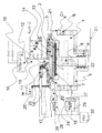
図3は、本発明を実施するために使用することができる薄膜形成装置の一例を示す。この薄膜形成装置を使って、処理ターゲットである半導体基板を真空移送室(図示せず)から反応室1に移送することができ、この反応室1内で薄膜形成プロセスを実施することができる。この反応室は、上蓋2、分散板3、排気ダクト4、下室5、基板移送ゲート6、排気口7、基板ヒータ8、および基板ヒータ上昇/下降ベローズ9を有する。反応室1に導入された後で、半導体基板を基板ヒータ上に置き、基板ヒータを上方に動かして分散板3と基板の間の距離が適切になるようにすることができる。
FIG. 3 shows an example of a thin film forming apparatus that can be used to implement the present invention. Using this thin film forming apparatus, a semiconductor substrate as a processing target can be transferred from a vacuum transfer chamber (not shown) to the reaction chamber 1, and a thin film forming process can be performed in the reaction chamber 1. The reaction chamber includes an
また、上蓋は、ガス導入パイプ10とガス導入部11に接続される。反応性ガスがパイプ10に接続され、反応性ガスをパージするための窒素ガスまたは不活性ガスも接続される。また、パイプ10は、ゲートバルブ11を介してラジカルソース12に接続され、ゲートバルブ11を開くことによって、ラジカルソース12で生成された様々な種類のラジカルガスを導入することができる。ガス導入部11は、ガス分散部13につながり、ガス導入部から導入されたガスはガス分散部13内で拡散し分散する。また、ガス導入部11は、ガスを分散するようにガス分散部13に導入することを可能にする分散構造を有することができる。分散部13内で拡散されたガスは、分散部13と分散板2の間の空間14に達する。ガス分散部13の先端と分散板2の間にスリット型排気口17が形成され、このスリットは、分散部13の先端に円形に設けられる。符号18は、この排気スリット17につながる空間であり、この空間18は、分散部13の外壁と上蓋2とによって形成され、ガス導入部11の周囲の空間につながる。
The upper lid is connected to the
上蓋上には、この空間18と排気バルブ20にも続く排気管19用のフランジ接続口が形成されている。一方、分散板2上に設けられたガス分散部13、空間14およびガス放出口21を通り最終的に基板加熱台8と分散板2の間の空間に達するガスは、更に、流れて基板15の表面に達し、次に排気ダクト4に形成されたリングスロット23を通ってスリットから続く排気管24から放出される。分散板3と基板加熱台8の間にプラズマを生成するために、分散板3に高周波導入端子25により高周波電極が導入される。
A flange connection port for the
図4(a)および(b)は、Ru膜の連続性を評価する方法を示す。図4(a)は、Ru膜が不連続な場合に該当し、図4(b)は、Ru膜が連続の場合に該当する。SiO2膜403上にWNC膜402を形成し、次にRu膜401または401’を形成し、その後で、得られた試料を、WNC膜を溶かすことができるウェットエッチング溶液404(塩酸と過酸化水素から成る混酸)に浸し、WNC膜からウェットエッチング溶液404に溶出したタングステン(W)405の量をICP質量分析によって測定し定量化することができる。(a)の概略図は、Ru膜401が連続的でないときにWNC膜がピンホールによってエッチングされる状態を示す。一方、(b)は、Ru膜401'は、コア密度が高い場合に連続であり、この場合、ウェットエッチング溶液がWNC膜に到達できず、従ってWNC膜から溶出したタングステン原子はエッチング溶液中に検出されない。ウェットエッチング溶液は、WNC膜をエッチングして溶出させるHCL、H2O2およびH2Oが1:1:20で混合された混酸であるが、この溶液はRu膜をエッチングしない。従って、Ru膜が連続的でない場合は、下層のWNC膜がエッチングされ、その成分が溶出する。従って、ICP質量分析によりエッチング溶液を測定することによってWの量を検出することができる。
4A and 4B show a method for evaluating the continuity of the Ru film. 4A corresponds to the case where the Ru film is discontinuous, and FIG. 4B corresponds to the case where the Ru film is continuous. A
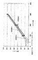
図5は、図2(a)、(b)または(c)に示したRu原料を使用したときのサイクル数に対するRu成長速度の依存を示す。膜形成条件は、後で実施例2で説明する。サイクル数に関しては、実施例2の表2に示した段階が1つのサイクルを構成するものとして定義し、このサイクルを繰り返す回数を数えた。図2(a)、(b)および(c)のRu原料の放置サイクル(厚さとサイクル数の比例関係を推定することによって得られる厚さが零の点に対応する)は、それぞれ37サイクル、30サイクルおよび54サイクルであった。 FIG. 5 shows the dependence of the Ru growth rate on the number of cycles when the Ru raw material shown in FIG. 2 (a), (b) or (c) is used. The film forming conditions will be described later in Example 2. Regarding the number of cycles, the stage shown in Table 2 of Example 2 was defined as constituting one cycle, and the number of times this cycle was repeated was counted. 2 (a), (b) and (c), the Ru raw material leaving cycle (corresponding to a point where the thickness obtained by estimating the proportional relationship between the thickness and the number of cycles corresponds to zero) is 37 cycles, There were 30 cycles and 54 cycles.
図6は、図5で形成されたRu膜のサイクル数と、図4に示した方法を使用して得られたWの検出量との関係を示す。ここで、収集率は、W原子がすべてエッチング溶液に溶出したと仮定して、Ru膜の下のWNC膜中の全W原子に対する検出されたW原子の実際の量の比率を示す。100%は、完全にエッチングされたことを示し、1%は、W原子全体の1%に対応するWの量が検出されたことを示す。図2(a)と(b)のRu前駆体の場合は、50サイクル後にほとんど完全な連続膜が形成された。一方、図2(c)のRu前駆体の場合は、200サイクルで連続膜は形成されなかった。 FIG. 6 shows the relationship between the number of cycles of the Ru film formed in FIG. 5 and the detected amount of W obtained using the method shown in FIG. Here, the collection rate indicates the ratio of the actual amount of detected W atoms to the total W atoms in the WNC film under the Ru film, assuming that all W atoms have eluted into the etching solution. 100% indicates complete etching, and 1% indicates that an amount of W corresponding to 1% of all W atoms has been detected. In the case of the Ru precursors of FIGS. 2 (a) and (b), an almost complete continuous film was formed after 50 cycles. On the other hand, in the case of the Ru precursor of FIG. 2C, a continuous film was not formed in 200 cycles.
図7は、前述のプロセスをデュアルダマシンCu配線プロセスに適用した場合のプロセスフローを示す。 FIG. 7 shows a process flow when the above-described process is applied to a dual damascene Cu wiring process.
図7(a)から図7(d)は、半導体素子の配線構造を示す概略断面図であり、本発明の一実施形態によるデュアルダマシン銅配線構造を形成するプロセスを説明するために示されている。具体的には、これらの図は、ALD法を使用して金属バリア膜を有するデュアルダマシン構造内のトレンチとコンタクトビアの表面全体をライニングし、その後でRu膜と銅層を形成するプロセスを説明している。 FIGS. 7A to 7D are schematic cross-sectional views showing a wiring structure of a semiconductor device, and are shown for explaining a process of forming a dual damascene copper wiring structure according to an embodiment of the present invention. Yes. Specifically, these figures illustrate the process of lining the entire surface of the trench and contact via in a dual damascene structure with a metal barrier film using ALD and then forming a Ru film and a copper layer. doing.
図7(a)は、金属バリア層を形成する前のデュアルダマシン構造を示す。導電性配線層201上に絶縁拡散バリア202を形成し、絶縁拡散バリア202の上にボトム絶縁体層203を形成し、ボトム絶縁体層203上にエッチングストップ層204を形成する。トップ絶縁体層205は、エッチングストップ層204の上に形成される。エッチングストップ層204は、所望の配線パターンのトレンチ208を形成するために使用される。トレンチ208は、エッチングマスク層レベルにエッチングされ、2つの絶縁体層205、203間に形成される。エッチングストップ層204は、トップ絶縁体層205の形成前にパターン形成されエッチングされ、トレンチ208の底から延在するコンタクトビアの所望の水平寸法を明確に画定するハードマスクを構成する。ハードマスクを含むエッチングストップ層204をエッチングする領域内で、トレンチ208の底から低導電性配線層201につながるコンタクトビア207が開けられる。符号206は、平坦化段階で化学機械的研磨が止められる層を示す。
FIG. 7A shows a dual damascene structure before forming a metal barrier layer. An insulating
図7(b)は、本発明の一実施形態における前処理工程を示す。この工程は、コンタクトビア207の底の銅配線面上に形成された酸化物を除去する段階と、ダマシン構造に露出された層間絶縁膜203、205の表面を前処理する段階(例えば、H2/Heガスを800WのRF出力で30秒間導入し、次にH2/H2/N2混合ガスを300WのRF出力で60秒間導入するによって)を含む。これにより、ダマシン構造の層間絶縁膜の表面が−NH結合と−NH2結合で終端する。この終端は、NH3ガスを使用する単純な熱処理だけで実現するのは難しい。しかしながら、高周波を使用してNH3を活性化すると、その表面を、プラズマで活性化させたH2/H2/N2混合ガスを使用するときと全く同じようにNH結合とNH2結合を使用して終端させることができる。
FIG. 7B shows a pretreatment process in one embodiment of the present invention. In this step, the oxide formed on the copper wiring surface at the bottom of the contact via 207 is removed, and the surface of the interlayer insulating
SiO2、SiOC、SiOなどの表面にアミノ基が導入される場合は、表面の原子に対するNの配位数は1であるなら、3配位原子であるNは表面上の原子と結合し、表面は−NH2で終端する。配位数が2の場合、表面は>NHで終端する。換言すると、本発明の一実施形態で望ましい表面終端構造は、−NH2か>NHである。後述するように、TEBガスや他の還元ガスは、図4に示したような−NH2結合またはNH結合内でHの置換の形で吸着されると考えられ、従って、表面には−NH2か>NHがなければならない。例えば、Si−NH−SiやSiONHOSiの場合には>NHが生じる。図7(b)では、−NHxの「x」は1か2を表わす。 When an amino group is introduced on the surface of SiO 2 , SiOC, SiO or the like, if the coordination number of N to the surface atom is 1, N that is a tricoordinate atom is bonded to an atom on the surface; surface terminates in -NH 2. When the coordination number is 2, the surface terminates with> NH. In other words, a desirable surface termination structure in one embodiment of the present invention is —NH 2 or> NH. As will be described later, TEB gas and other reducing gases are considered to be adsorbed in the form of substitution of H within —NH 2 bonds or NH bonds as shown in FIG. There must be 2 or> NH. For example,> NH occurs in the case of Si—NH—Si or SiONHOSi. In FIG. 7B, “x” in —NH x represents 1 or 2.
一実施形態において、表面へのアミノ基の導入は、低誘電率の膜の表面だけでなく、図7(b)に示したようなビアの底の金属配線層の表面にも行われる。 In one embodiment, amino groups are introduced into the surface not only on the surface of the low dielectric constant film but also on the surface of the metal wiring layer at the bottom of the via as shown in FIG. 7B.
図7(a)に示した絶縁膜205、203として、次世代素子に幅広く使用されるであろうSiOC低誘電率膜が利用される場合は、アルキル基であるメチル基鎖などのSiOC膜中の炭素含有側鎖が、NH3ガスによる高周波プラズマによってエッチングされ、その結果SiOC膜中のCH3、C2H5や他のアルキル基が失われる。これにより、しばしばコンタクトビア207が樽形に変形する。高周波プラズマによって絶縁膜205、203が破損される可能性がある場合は、H2/He/N2ガスによる高周波プラズマを使用することにより、SiOC膜上の悪影響を軽減することができる。一実施形態では、H2/He/N2中の窒素の分圧は、5〜50%であり、より好ましくは10〜30%である。RF出力周波数は、13.56MHz(通常は2MHz以上60MHz以下)に調整することができる。Heの他に、Arや他の不活性ガスも使用することができる。一実施形態では、処理条件を以下のように設定することができる。
In the case where a SiOC low dielectric constant film that will be widely used in next-generation devices is used as the insulating
以上の説明で、「プラズマ」は、例えばシャワーヘッドと基板が乗せられた加熱台の間に印加される13.56kHzの高周波RF波によって生成される平行平板プラズマと呼ばれるものを指す。換言すると、基板はプラズマ生成雰囲気中にある。従って、このプロセスは、イオン活性種などのプラズマ中に生成され寿命の短い活性種による影響を受ける。一方で、基板から遠い場所にプラズマを生成する方法(遠隔プラズマ装置を使用する)があり、活性化された分子の間で、長い寿命を有する中性分子が基板まで移送され表面処理に使用される。これは、ラジカルプロセスと呼ばれる。換言すると、「ラジカル」は、電子が安定しているノーマル(基底)状態に対して、電子が励起された状態の分子を指す。ラジカルはイオンではないが、活性化されており反応性である。本発明の一実施形態では、プラズマとラジカルを交換可能に使用することができる。当業者は、適切なラジカル生成条件を、対応するプラズマ生成条件から決定できるはずである。 In the above description, “plasma” refers to what is called parallel plate plasma generated by a high frequency RF wave of 13.56 kHz applied between a heating head on which a shower head and a substrate are placed, for example. In other words, the substrate is in a plasma generation atmosphere. Therefore, this process is influenced by active species that are generated in plasma such as ion active species and have a short lifetime. On the other hand, there is a method of generating plasma in a place far from the substrate (using a remote plasma device), and between activated molecules, neutral molecules having a long lifetime are transferred to the substrate and used for surface treatment. The This is called a radical process. In other words, “radical” refers to a molecule in which electrons are excited relative to a normal (ground) state in which electrons are stable. Radicals are not ions, but are activated and reactive. In one embodiment of the present invention, plasma and radicals can be used interchangeably. One skilled in the art should be able to determine the appropriate radical production conditions from the corresponding plasma production conditions.
前述のプロセスでは、アミノ基がプラズマによって表面に導入される。プラズマを使用せずにアミノ基を熱的に導入するのは困難である。例えば、NH3を供給するだけでアミノ基を導入することは困難である。しかしながら、表面へのアミノ基の導入は、N2H2ガス(ヒドラジン)などを使用すれば、プラズマを使用することなく可能である。一実施形態では、ヒドラジンを使用するプロセス条件を以下のように設定することができる。全流量に対するヒドラジンの分圧は、10〜50%であることが好ましい。 In the aforementioned process, amino groups are introduced to the surface by plasma. It is difficult to thermally introduce amino groups without using plasma. For example, it is difficult to introduce an amino group simply by supplying NH 3 . However, introduction of amino groups on the surface is possible without using plasma if N 2 H 2 gas (hydrazine) or the like is used. In one embodiment, the process conditions using hydrazine can be set as follows. The partial pressure of hydrazine with respect to the total flow rate is preferably 10 to 50%.
図7(c)によって示した段階では、TEB(トリエチルボロン)ガスや他の還元ガスを導入して次に不活性ガスでパージし、その後で、WF6ガスや他の金属ハロゲン化物を導入して次に不活性ガスでパージし、その後で、NH3ガスや他のハロゲン置換窒化物ガスを導入して次に不活性ガスでパージする。これらの導入とパージを繰り返すことによって、ダマシン構造の表面に、金属原子(金属バリア膜とも呼ばれる)209を含む滑らかなWNC膜や他のバリア膜を形成することができる。バリア膜は、導電膜と呼ばれることがあるが、この用語の使用は、絶縁膜との差を強調する状況に限られる。バリア膜は必ずしも導電性とは限らない。 At the stage shown in FIG. 7 (c), TEB (triethylboron) gas or other reducing gas is introduced and then purged with an inert gas, and then WF 6 gas or other metal halide is introduced. Then purge with an inert gas, then introduce NH 3 gas or other halogen-substituted nitride gas and then purge with inert gas. By repeating these introduction and purging, a smooth WNC film or other barrier film containing metal atoms (also called a metal barrier film) 209 can be formed on the surface of the damascene structure. Although the barrier film may be referred to as a conductive film, the use of this term is limited to a situation that emphasizes the difference from the insulating film. The barrier film is not necessarily conductive.
還元ガスに関しては、TEBの代わりに、B2H6、アルキルボロン化合物、SiH4、Si2H6、またはアルキルシリコン化合物を使用することができる。金属ハロゲン化物に関しては、WF6の代わりにTaF6またはTiCl4を使用することができる。その結果、WNC膜の代わりに、金属原子を含むバリア膜をTaN、TaCN、WN、TiNまたはTiCN膜として形成することができる。 Regarding the reducing gas, B 2 H 6 , an alkyl boron compound, SiH 4 , Si 2 H 6 , or an alkyl silicon compound can be used instead of TEB. For metal halides, TaF 6 or TiCl 4 can be used instead of WF 6 . As a result, a barrier film containing metal atoms can be formed as a TaN, TaCN, WN, TiN or TiCN film instead of the WNC film.
前に述べたように、前述のバリア膜を形成した表面はアミノ基で終端する。還元ガスを導入し、金属ハロゲン化物を導入し、次にハロゲン置換窒化物ガスを導入するプロセスを繰り返すことによって、滑らかで均一のバリア膜を形成することができる。米国特許第6,759,325号は、ダマシン配線構造を形成するトレンチとビアの内表面にWF6を吸着させ、次にTEBや他の還元ガスを使用して還元させる方法を開示している。しかしながら、金属ハロゲン化物前駆体を導入すると、層間絶縁膜が破損したり膜内への浸透が生じたりすることがある。 As described above, the surface on which the aforementioned barrier film is formed terminates with an amino group. By repeating the process of introducing the reducing gas, introducing the metal halide, and then introducing the halogen-substituted nitride gas, a smooth and uniform barrier film can be formed. U.S. Pat. No. 6,759,325 discloses a method of adsorbing WF 6 on the inner surfaces of trenches and vias forming a damascene interconnect structure and then reducing using TEB or other reducing gas. . However, when a metal halide precursor is introduced, the interlayer insulating film may be damaged or may penetrate into the film.
一実施形態では、バリア膜の厚さは、1〜5nmの範囲、好ましくは2〜4nmの範囲に調整される。 In one embodiment, the thickness of the barrier film is adjusted in the range of 1-5 nm, preferably in the range of 2-4 nm.
図7(d)によって示した段階では、Ru膜などの第2の金属膜210が、プラズマALDや他の方法を使用してWNC膜などのバリア膜209上に形成される。ここで、第2の金属膜は、前処理の後で形成された金属バリア膜の上に形成される。この膜は、配線に使用される銅膜との良好な接着を示すRu、Ta、その他の材料を含み、いわゆる接着層または粘着層として働く。換言すると、この膜は、銅配線と、銅拡散バリアとして働く導電膜の間に挟まれており、この2つの間の接着力を高める。
At the stage shown in FIG. 7D, a
Ru−ALDは、前述の化合物とNH3プラズマを交互に供給するプラズマALD法によって形成することができる。Ru膜が還元雰囲気中で形成されるので、WNC膜209を酸化することなく積層構造を作成することができる。
Ru-ALD can be formed by a plasma ALD method in which the aforementioned compound and NH 3 plasma are alternately supplied. Since the Ru film is formed in a reducing atmosphere, a laminated structure can be created without oxidizing the
一実施形態では、第2の金属膜の厚さは、1〜10nmの範囲、または好ましくは1〜3nmの範囲に調整される。 In one embodiment, the thickness of the second metal film is adjusted in the range of 1-10 nm, or preferably in the range of 1-3 nm.
図7(e)は、ビア/トレンチを銅で埋めるために銅211を散布する段階を示す。図7(f)で、ビア/トレンチの上の余分な銅層をCMPによって除去し、素子の表面がCMPによって更に平坦化され、その結果、WNC膜209とRu膜210を上面から除去し、それにより相互接続銅線212が形成される。
FIG. 7 (e) shows the step of spreading
以上において、第1のRF出力の周波数は、13MHz〜30MHzでもよく、第2のRF出力の周波数は、300kHz〜450kHzでもよい。第2のRF出力は、第1のRF出力より低くてもよい。上記の条件に従って、厚さが約2〜約10nm、好ましくは約2nm〜約5nmのSiC膜を形成することができる。 In the above, the frequency of the first RF output may be 13 MHz to 30 MHz, and the frequency of the second RF output may be 300 kHz to 450 kHz. The second RF power may be lower than the first RF power. According to the above conditions, a SiC film having a thickness of about 2 to about 10 nm, preferably about 2 nm to about 5 nm can be formed.
図8(b)は、本発明の一実施形態で使用可能な処理装置の例を示す構造図である。この装置は、様々な工程段階を処理するクラスタ型構造を有する。図8(a)は、本発明の一実施形態によるプロセスフローを示す。点線で囲まれた段階は、図8(b)に示した装置内で処理される。 FIG. 8B is a structural diagram showing an example of a processing apparatus that can be used in an embodiment of the present invention. The apparatus has a clustered structure that processes various process steps. FIG. 8 (a) shows a process flow according to one embodiment of the present invention. The stage surrounded by the dotted line is processed in the apparatus shown in FIG.
図8(b)では、例えば、基板が、大気圧ロボット301によってカセットボックス300からロードロック室302に移され、その後で、基板は、N2/H2/Heガスを使用するプラズマプロセスに基づく前処理にかけるために、中央プラットフォーム303に備えられた中央ハンドラ303によって前処理モジュール304に移される。次に、前処理された基板は、真空中でWNC−ALDモジュール305に移されてWNC−ALDプロセスにかけ、次に真空中でRuALDモジュール306に移されてRu−ALD膜が形成される。WNC膜の表面は、大気と接触すると酸化し易いので、前述のように、真空中で基板を移送することは、Ru−ALD膜を形成する際に極めて有効である。
In FIG. 8 (b), for example, the substrate is transferred from the
図9(a)は、本発明の一実施例において、本発明によって提案された方法に従ってWNC上にRu膜を形成する段階と、CVDによって酸化雰囲気中でRu膜を形成する段階とを含むプロセスを実施するために使用される反応装置の構造の一例を示す。この薄膜形成装置によって、処理ターゲットである半導体基板を、ゲートバルブ102を介して真空移送室(図示せず)から反応室101内に移すことができ、この反応室101内で薄膜形成プロセスを実行することができる。移された基板114は、加熱台102上に配置され、その環境を、バルブ127を介してターボ分子ポンプ128(TMP)を使用して真空にすることができる。その後で、基板加熱台102は、ベローズ114によって、シャワープレートからの距離が最適になるまで上昇される。その結果、シャワープレートから供給される反応性ガスが、基板114の表面に供給され、次に排気ダクト103から放出される。この時点で、シャワープレート104から供給される反応性ガスが、ベローズ114が配置された移送側に拡散するのを防ぐために、バルブ131を開けて不活性ガスを供給することができる。
FIG. 9 (a) shows, in one embodiment of the present invention, a process including forming a Ru film on a WNC according to the method proposed by the present invention and forming a Ru film in an oxidizing atmosphere by CVD. An example of the structure of the reactor used in order to implement is shown. With this thin film forming apparatus, a semiconductor substrate as a processing target can be transferred from a vacuum transfer chamber (not shown) into the
この反応室は、排気ダクト103、シャワープレート104、および上蓋113が次々と上に配置された積層構造を有し、ガス導入パイプ110に続くガス分散ノズル111(図9(b))とガス分散ガイド108が、シャワープレート104と上蓋113の間に配置されている。更に、ガス分散ガイドに沿って、分散部を排気するための排気バルブ109が接続される。また、ガス導入部105、ガス導入バルブ124、およびガス排出弁132は、シャワープレート104に接続される。パージ用の不活性ガス導入バルブ123も接続される。更に、ガス導入バルブ121とパージ用の不活性ガス導入バルブ120が、ガス導入パイプ110に接続される。Ru原料ガスがバルブ121から導入される。また、不活性ガスを速い流量で導入するバルブ122が形成される。バルブ121からガス導入パイプ110に導入されたRu原料は、ガス分散ノズル111によって分散され、ガス分散ガイドに沿って流れ、その後で、シャワープレート104のガス放出口112を通り、基板114上に供給される。一方、ガス弁124から供給されたNH3ガスまたはO2ガスは、シャワープレート104に設けられたガス導入部105内を通り、ガス分散室107内に拡散し、次にガス放出口106から基板114上に供給される。この時点で、シャワープレート104に高周波が印加され、アースされた基板加熱台102とシャワープレート104の間にプラズマが励起されて、NH3プラズマによって基板106の表面が処理される。また、基板114上に供給されたガスは、排気ダクト103を介して、排気バルブ125と圧力制御装置(APC)126によって、真空ポンプ130によって放出される。
This reaction chamber has a laminated structure in which an exhaust duct 103, a shower plate 104, and an
反応性ガスをパージするときは、不活性ガスがガス弁120と122によって導入され、排気バルブ109が、残っているRu原料を放出するために開かれる。この時点で、残っているRu原料は、ガス放出口112を介して排気ダクト103から放出されるが、装置は、バルブ109内の排気コンダクタンスが少なくとも1桁高くなるように設計され、従って残っているガスのほとんどが排気バルブ109を通って放出される。ガス弁124から供給されたNH3ガスをパージするとき、同様に不活性ガスがバルブ123から導入され、残っているガスが放出するために排気バルブ132が開かれる。この時点で、排気ダクト103を介してガス放出口106から多少のガスが放出されるが、排気バルブ132のガス排出コンダクタンスは、ガス放出口106のものより大きいので、ほとんどのガスが排気バルブ132から放出される。
When purging reactive gas, inert gas is introduced by
以上の機能を利用することによって、反応性Ru原料ガスを交互に供給する原子層堆積プロセス、即ち一層づつの薄膜を形成するプロセスに理想的なプロセス装置を提供することができる。 By utilizing the above functions, it is possible to provide an ideal process apparatus for an atomic layer deposition process in which reactive Ru source gases are alternately supplied, that is, a process for forming a single thin film.
また、Ru原料とO2ガスを同時に供給することによって、化学蒸着法を実施することができる。この場合、バルブ121を通って供給されるRu原料は、ガス放出口112を通り、基板表面に供給され、バルブ24を通って供給されたO2ガスは、ガス放出口6を通り、基板表面に供給される。Ru原料とO2が、基板表面で化学蒸着反応によって反応すると、薄いRu膜が形成される。
Further, the chemical vapor deposition method can be performed by simultaneously supplying the Ru raw material and the O 2 gas. In this case, the Ru raw material supplied through the
図10は、実施例3に説明されたキャパシタ電極の断面構造を示す概略図である。この構造は、本発明の実施形態に従ってWNxCy膜401上にRu膜402を形成し、次に化学蒸着法によってRu膜またはRuO2膜を上に堆積させることによって作成される。
FIG. 10 is a schematic diagram illustrating a cross-sectional structure of the capacitor electrode described in the third embodiment. This structure is created by forming a
図11は、ALD−Ru膜のシート抵抗のサイクル数に対する依存性を示すグラフであり、シートは、WF6、NH3またはTEBガスを使用してALDによって形成されたALDWNC膜の上に、本発明の一実施形態によるRu膜を使用してNH3ガスとプラズマを利用するALDによってALD−Ru膜を形成し、次にその上に同じRu原料と酸素を使用してCVDによって形成されたRuCVD膜を積層することによって作成される。この例では、図2(a)に示したRu前駆体が使用される。 FIG. 11 is a graph showing the dependence of the sheet resistance of the ALD-Ru film on the number of cycles. The sheet is formed on the ALDWNC film formed by ALD using WF 6 , NH 3 or TEB gas. An ALD-Ru film is formed by ALD using NH 3 gas and plasma using a Ru film according to an embodiment of the invention, and then formed by CVD using the same Ru source and oxygen. Created by laminating films. In this example, the Ru precursor shown in FIG. 2A is used.
これらのサンプルの特定の構造を説明する。最初に、4つのタイプの下層のRu膜をプラズマALDによって形成した(実施例2の表2に示した膜形成条件に従って)。この4つのタイプは、25、50、75および100の異なるサイクル数に対応する(換言すると、実施例2の表2に示した4つの段階から成るサイクルはそれぞれ、25回、50回、75回および100回繰り返された)。このように作成された各Ru膜上に、化学蒸着法によってRuCVD膜を形成し、この膜を形成するのに必要な時間を水平軸によって示した。ここで、25サイクルのプラズマALDによって形成されたRu膜上に、酸化雰囲気中でRuCVD膜が形成されたとき、プラズマALDによるRu膜が連続的でないと、酸素ガスが下層WNC膜に拡散し酸化させる。その結果、本来時間とともに減少するものであるシート抵抗は逆に大きくなる。 The specific structure of these samples is described. First, four types of underlying Ru films were formed by plasma ALD (according to the film formation conditions shown in Table 2 of Example 2). The four types correspond to 25, 50, 75 and 100 different cycle numbers (in other words, the four-stage cycle shown in Table 2 of Example 2 is 25 times, 50 times and 75 times, respectively. And repeated 100 times). A RuCVD film was formed by chemical vapor deposition on each Ru film formed in this way, and the time required to form this film is indicated by the horizontal axis. Here, when a RuCVD film is formed in an oxidizing atmosphere on a Ru film formed by 25 cycles of plasma ALD, if the Ru film by plasma ALD is not continuous, oxygen gas diffuses into the lower WNC film and oxidizes. Let As a result, the sheet resistance, which originally decreases with time, increases conversely.
一方、75サイクルと100サイクルのプラズマALDによって形成されたRu膜上に化学蒸着法によってRuCVD膜を形成しても抵抗は増大せず、下層のWNC膜は酸化しない。 On the other hand, even if a RuCVD film is formed by chemical vapor deposition on a Ru film formed by 75 cycles and 100 cycles of plasma ALD, the resistance does not increase and the underlying WNC film is not oxidized.
図12(a)は、本発明の実施形態で使用することができる形成装置の構造の一例を示し、Ru膜402を形成するために使用される原料は、化学蒸着法によってRu膜403を形成するために使用される原料と異なる。図9(a)に示した構造を構成するものと同じ構成要素は、同じ符号で示されている。図9(a)との違いは、図12(a)では、第2のRu原料(Ru(C))を供給する原料供給容器138が提供されていることである。この原料供給容器138は、キャリアガス導入バルブ136を介してキャリアガス供給ライン133に接続され、原料供給バルブ137を介して反応装置にも接続される。この図では、Ru(A)とRu(C)は、同じラインによって反応装置に供給される。しかしながら、原料を供給する方法はこの構成に限定されず、別のラインを使用してそれぞれの原料を反応装置に供給することができる。
FIG. 12A shows an example of the structure of a forming apparatus that can be used in the embodiment of the present invention, and the raw material used to form the
前述の図1〜図12を使用して特定の実施例を説明する。 A specific embodiment will be described with reference to FIGS.
(実施例1)
図1(b)のプロセスシーケンスによれば、金属膜を形成し、次にアンモニアプラズマALDに基づくRu原料を使用してRu膜を形成するプロセスで、下層金属膜として、ALDによって形成されたWNC膜を使用した。WNC膜は、WF6、NH3またはTEB(トリエチルボロン)を使用するプロセスによって形成された(実施例2の表1に示した条件で)。Ru−ALD膜は、図2(a)、(b)および(c)に示したRu原料と、図3に示した形成装置とを使用して形成された(実施例2の表2に示した条件で)。その結果を比較して、膜ごとにピンホールとサイクル数の関係を調べた。
Example 1
According to the process sequence of FIG. 1B, a WNC formed by ALD as a lower metal film in a process of forming a metal film and then forming a Ru film using a Ru raw material based on ammonia plasma ALD. A membrane was used. The WNC film was formed by a process using WF 6 , NH 3 or TEB (triethyl boron) (under the conditions shown in Table 1 of Example 2). The Ru-ALD film was formed by using the Ru raw material shown in FIGS. 2A, 2B and 2C and the forming apparatus shown in FIG. 3 (shown in Table 2 of Example 2). Under the conditions). The results were compared, and the relationship between pinholes and the number of cycles was investigated for each film.
図5は、Ru膜の厚さとサイクル数の関係を示す。図2(c)に示した前駆体は、(以下、「前駆体C」と呼ぶ)は、57サイクル必要とし、図2(a)に示した前駆体(以下、「前駆体A」と呼ぶ)と図2(b)に示した前駆体(以下「前駆体B」と呼ぶ)はそれぞれ、37サイクルと35サイクルを必要とする。図6は、各膜ごとに現れたピンホールとサイクル数の関係を示す。図4に示した方法を使用してRu/WNC層膜を形成したチップの単位面積から溶出したタングステンの量をICP法に基づいて定量分析することにより、WNC膜中の全タングステン含有量に対する溶出したタングステンの割合を測定した。 FIG. 5 shows the relationship between the Ru film thickness and the number of cycles. The precursor shown in FIG. 2C (hereinafter referred to as “precursor C”) requires 57 cycles, and the precursor shown in FIG. 2A (hereinafter referred to as “precursor A”). ) And the precursor shown in FIG. 2B (hereinafter referred to as “precursor B”) require 37 cycles and 35 cycles, respectively. FIG. 6 shows the relationship between pinholes appearing for each film and the number of cycles. The amount of tungsten eluted from the unit area of the chip on which the Ru / WNC layer film is formed using the method shown in FIG. 4 is quantitatively analyzed based on the ICP method, so that the elution with respect to the total tungsten content in the WNC film is achieved. The proportion of tungsten made was measured.
図6は、図2(a)と(b)に示したRu原料の様々な収集率(%)に対応するサイクル数を示す。これらのRu原料の場合、収集率は、約50サイクルと55サイクル以上でそれぞれ0%になった。タングステンは収集率%でエッチング液に溶出しないので、これらのサイクルで連続膜が形成されたことが分かる。一方、図2(c)に示したRu原料の場合、ほぼ0%の収集率を達成するには約200膜形成サイクルが必要であり、その点で、タングステン溶出はないと考えられる。図1に示したようなNH3プラズマを使用する連続プロセスは、前駆体AやBなどのペンタジエニル基を有するRu分子を使用すると、連続膜を短いサイクルで形成することができる。しかしながら、前駆体Cなどのシクロペンタジエニル基だけを有するRu分子の場合は、少なくとも200サイクルで連続膜を形成することはできない。 FIG. 6 shows the number of cycles corresponding to various collection rates (%) of the Ru raw materials shown in FIGS. 2 (a) and 2 (b). In the case of these Ru raw materials, the collection rates became 0% at about 50 cycles and 55 cycles or more, respectively. Since tungsten does not elute into the etchant at a collection rate of%, it can be seen that a continuous film was formed in these cycles. On the other hand, in the case of the Ru raw material shown in FIG. 2 (c), about 200 film formation cycles are necessary to achieve a collection rate of almost 0%, and it is considered that there is no tungsten elution. In the continuous process using NH 3 plasma as shown in FIG. 1, when Ru molecules having pentadienyl groups such as precursors A and B are used, a continuous film can be formed in a short cycle. However, in the case of Ru molecules having only a cyclopentadienyl group such as the precursor C, a continuous film cannot be formed in at least 200 cycles.
図5に示したように、1サイクル当たりの膜成長速度は、Ru分子とほぼ等しいが、必要な放置時間は、前駆体A、BおよびCの間でそれぞれ37サイクル、30サイクルおよび54サイクルと変化した。形成された膜が連続であると考えられるサイクル数が、それぞれ50サイクル、50サイクル、および200サイクルであったとき、得られた膜厚は、それぞれ0.44nm、0.3nm、および3.4nmであった。従って、図2(a)と(b)に示した原料の場合、膜は、膜厚が0.5nm以上の場合に十分に連続的になる。また、実際には、半導体素子には平坦部分と段差部分があり、NH3プラズマと共にRu原料を使用するプロセスは、アスペクト比が5の穴に対して70%の被覆率を提供することが分かった。換言すると、素子被覆率も考慮すると0.7nm以上の厚さで連続膜を得ることができる。実際には、膜厚を0.7〜1.0nmの範囲内で制御することが好ましい。また、より大きなマージンを達成できるので、1.0nm以上の厚さで高い信頼性を保証することができる。 As shown in FIG. 5, the film growth rate per cycle is almost the same as that of the Ru molecule, but the required standing time is 37 cycles, 30 cycles and 54 cycles between the precursors A, B and C, respectively. changed. When the number of cycles that the formed film was considered to be continuous was 50 cycles, 50 cycles, and 200 cycles, respectively, the obtained film thicknesses were 0.44 nm, 0.3 nm, and 3.4 nm, respectively. Met. Therefore, in the case of the raw materials shown in FIGS. 2A and 2B, the film is sufficiently continuous when the film thickness is 0.5 nm or more. In fact, the semiconductor device has a flat portion and a step portion, and it is found that the process using Ru raw material together with NH 3 plasma provides a coverage of 70% for a hole with an aspect ratio of 5. It was. In other words, considering the element coverage, a continuous film can be obtained with a thickness of 0.7 nm or more. Actually, it is preferable to control the film thickness within a range of 0.7 to 1.0 nm. Further, since a larger margin can be achieved, high reliability can be ensured with a thickness of 1.0 nm or more.
一方、図2(c)に示したRu原料を使用する場合は、膜が連続しなくなる最小厚さは約3〜4nmであり、すなわち、実際にはRu膜は4nm以上の厚さでなければならない。その結果、実際の銅配線にこのRu原料を使用すると、Ru膜の厚さが増えるので銅配線量が減少し、それにより実質的に配線抵抗が高くなる。この問題を防ぐために、より薄いRu膜が必要である。本発明によって提案される方法によって、1nm以下の厚さのRu膜の使用が可能になるので、銅配線とRu間の良好な接着力を保証しながら銅体積を増やし配線抵抗を減少させることができる。 On the other hand, when the Ru raw material shown in FIG. 2 (c) is used, the minimum thickness at which the film is not continuous is about 3 to 4 nm, that is, the Ru film is not actually thicker than 4 nm. Don't be. As a result, when this Ru raw material is used for actual copper wiring, the thickness of the Ru film increases, so that the amount of copper wiring decreases, thereby substantially increasing the wiring resistance. In order to prevent this problem, a thinner Ru film is required. The method proposed by the present invention makes it possible to use a Ru film with a thickness of 1 nm or less, so that it is possible to increase the copper volume and reduce the wiring resistance while ensuring good adhesion between the copper wiring and Ru. it can.
ペンタジエニル基を有するRu原料の場合、この実施例で説明したようなNH3プラズマを使用するALD法によって、Ru成分をNH3プラズマによって容易に分離することができ、従ってコア形成密度が向上し、それにより連続膜を小さな膜厚で容易に形成できることが分かる。一方、Ru原料がシクロペンタジエニルだけを有する場合は、シクロペンタジエニルは、NH3プラズマの下でも容易に分離せず、従って連続膜は容易に形成されない。 In the case of a Ru raw material having a pentadienyl group, the Ru component can be easily separated by NH 3 plasma by the ALD method using NH 3 plasma as described in this example, so that the core formation density is improved. This shows that a continuous film can be easily formed with a small film thickness. On the other hand, when the Ru raw material has only cyclopentadienyl, cyclopentadienyl is not easily separated even under NH 3 plasma, and therefore a continuous film is not easily formed.
(実施例2)
この実施例は、最も一般的に使用される銅配線構造であるデュアルダマシン構造を使用する配線プロセスの形成に対する本発明の適用と、そのような適用の効果を示す。
(Example 2)
This example illustrates the application of the present invention to the formation of a wiring process using a dual damascene structure, the most commonly used copper wiring structure, and the effects of such application.
図7は、デュアルダマシン構造を形成するプロセスを示す。図7(a)〜(f)は、デュアルダマシン処理の完了後の状態から始まるプロセスフローを示す。図8(a)と(b)は、この実施例で使用されるクラスタ装置(図8(b))の構造とクラスタプロセスシーケンス(図8(a))を示す。図8(b)に示したクラスタ装置は、前処理モジュール304、WNxCy膜形成モジュール305、およびRu形成モジュール306を含み、図8(a)に示したような連続真空サイクルに基づいてプロセスを実行する。図7(a)は、デュアルダマシン処理の完了後の状態を示す。SiOC膜202、層間絶縁膜203、エッチングストッパ膜204、層間絶縁膜205および銅拡散防止膜206が、下層の銅配線201上に形成されて、銅拡散防止層が作成される。この条件で、ALDバリア膜の形成前に、図8に示した前処理モジュール304を使用して前処理が実行される。図7(b)は、前処理直後の状態を示す。ここで、銅配線203の表面上のコンタクトビア207の底に形成された酸化物を還元する段階が、デュアルダマシン構造のトレンチ208とコンタクトビア207の上に層間絶縁膜を構成する202、203、204、205および206の処理端の表面を安定させる処理と同時に実行される。この処理は、表面にNH基またはNH2基を形成する。この表面処理は、次の段階でWNxCy膜のスムーズな形成を可能にする。その表面を、図8(b)に示した前処理モジュール304によって処理した後で、基板は、WNC膜を形成するために図8(b)に示したようなWNC−ALD形成305のための処理モジュールに移される。表1は、ここで実施されるWNC−ALD形成の条件を示す(表に示した値は、±50%の範囲内で修正することができる)。
FIG. 7 illustrates a process for forming a dual damascene structure. FIGS. 7A to 7F show a process flow starting from the state after the completion of the dual damascene process. FIGS. 8A and 8B show the structure of the cluster apparatus (FIG. 8B) used in this embodiment and the cluster process sequence (FIG. 8A). The cluster apparatus shown in FIG. 8B includes a

以上の段階を繰り返すことによって、図7(c)に示したように、3nmのWNC膜209をスムーズに形成することができる。次に図7(d)で、図8(b)に示したRu−ALDモジュール305を使用してRu膜210を形成する。ここでは、図2(a)に示したRu原料を使用し、図1(a)に示したシーケンスに従うNH3プラズマプロセスで原料を処理した。表2は、Ru−ALD処理条件を示す。NH3プラズマのRF出力として800Wを使用したが、200〜1、000WのRF出力範囲でRu膜を形成することができる。また、250〜400℃の範囲の形成温度で類似のプロセスを達成することができる。100サイクルで約1nmの厚さのRu膜が形成された(下の表2に示した条件で。表に示した値は、±50%の範囲内で修正することができ、他のRu原料で同じようにプロセスを実行することができる。)。図8(b)に示した装置から移されたウェーハ上に、図7(d)に示したCuシード膜211が形成され、その後で、図7(e)に示したように銅めっき膜が形成されて、CMPによって銅配線212が形成される。また、Ru膜210を形成した後にCuめっきによってCu膜を形成してもよく、あるいはRu膜210上に直接Cuめっきを形成してもよい。Cu膜211の場合、PVDの代わりにCVDまたはALDによって形成したCu膜を使用することもできる。
By repeating the above steps, the 3
前述のように、表面処理、ALDによるWNC/Ru形成、およびCuめっきを含む一連の段階を連続的に実行することによって、高い信頼性を維持することができる。前述の方法によって形成された層状WNCとRu膜構造の厚さは4nmであり、これは、従来のバリア金属を使用したときより薄い。その結果、低抵抗の銅配線が得られた。 As described above, high reliability can be maintained by continuously executing a series of steps including surface treatment, WNC / Ru formation by ALD, and Cu plating. The thickness of the layered WNC and Ru film structure formed by the above method is 4 nm, which is thinner than when using a conventional barrier metal. As a result, a low resistance copper wiring was obtained.
(実施例3:Ru−CVD/Ru−ALDの実施例)
この実施例は、実施例1または2に示した極めて薄いRu膜、即ちCu膜接着層として使用される約1〜4nmのRu膜に関する。電極としてRu膜を使用するキャパシタの形成などの特定の用途では、Ru膜を約10〜20nmの厚さ範囲にもっと厚く形成しなければならない。しかしながら、実施例1または2に示したプロセスでは、10nmの膜を形成するには図1(a)に示したサイクルを500回繰り返さなければならない。1サイクルが完了するのに3秒かかる場合、サイクルタイムの合計は1,500秒になり、このため、半導体素子の生産性が大幅に低下する。一方、Ru膜を化学蒸着法によって形成する場合は、図2に示したRu原料と酸素ガスを使用してRu膜を形成することもでき、酸素分圧を調整することによってRuO2膜を形成することもできる。
(Example 3: Example of Ru-CVD / Ru-ALD)
This example relates to the extremely thin Ru film shown in Example 1 or 2, that is, about 1 to 4 nm of Ru film used as a Cu film adhesion layer. In certain applications, such as the formation of capacitors using Ru films as electrodes, the Ru film must be formed thicker in the thickness range of about 10-20 nm. However, in the process shown in Example 1 or 2, the cycle shown in FIG. 1A must be repeated 500 times to form a 10 nm film. If it takes 3 seconds to complete one cycle, the total cycle time is 1,500 seconds, and the productivity of the semiconductor device is greatly reduced. On the other hand, when the Ru film is formed by chemical vapor deposition, the Ru film can be formed using the Ru raw material and oxygen gas shown in FIG. 2, and the RuO 2 film is formed by adjusting the oxygen partial pressure. You can also
実施例1と2に示した構造は、一般的なキャパシタ電極と共に、Ru膜の下にWNxCy膜を使用するが、多結晶シリコンまたはTiN膜などが電極の下層として配置される。Ru膜が化学蒸着法によって形成される場合は、前述の多結晶シリコン、TiNなどの表面が酸化され、その結果接触抵抗が大きくなる。この実施例は、この酸化を抑えながらRu電極とRuO2電極をどのように形成できるかを示す。 The structures shown in the first and second embodiments use a WNxCy film under a Ru film together with a general capacitor electrode, but a polycrystalline silicon or TiN film is disposed as a lower layer of the electrode. When the Ru film is formed by a chemical vapor deposition method, the surface of the aforementioned polycrystalline silicon, TiN or the like is oxidized, resulting in an increase in contact resistance. This example shows how a Ru electrode and a RuO 2 electrode can be formed while suppressing this oxidation.
図9は、この実施例で使用されるRu膜形成装置の断面を示す構造図である。Ru前駆体Aが、バルブ121を介して供給され、NH3またはO2が、バルブ140または123を介して供給される。Arパージガスが、バルブ122と124を介して供給される。
FIG. 9 is a structural diagram showing a cross section of the Ru film forming apparatus used in this embodiment. Ru precursor A is supplied via
最初に、実施例2の表2に示した条件に基づいてNH3プラズマによる原子層堆積法によってRu膜を形成し、その後で、NH3をO2ガスに変更し、Ru前駆体Aと酸素ガスを、それぞれシャワーヘッドの112と107を介して供給した。2つのガスがシャワーヘッド内で混合しないので、これらのガスは、シャワーヘッド内で互いに反応しないが、基板106の表面で反応してRu膜を形成する。
First, a Ru film is formed by an atomic layer deposition method using NH 3 plasma based on the conditions shown in Table 2 of Example 2, and then NH 3 is changed to O 2 gas, and Ru precursor A and oxygen are changed. Gas was supplied through
図10は、WNC−ALD膜401上にRu−ALD膜402を形成し、次にRu膜403を化学蒸着法によって形成した断面構造を示す概略図である。Ru膜402が連続的でなく且つ酸化雰囲気にさらされた場合、下層のWNC膜401は酸化し易い。従って、Ru膜402を形成するために行われるサイクルの数を25、50、75および100に変更し、各サイクル数で作成されたRu膜上にRu膜403を形成した。図10は、シート抵抗が様々なサイクル数でどのように変化したかを示す。
FIG. 10 is a schematic view showing a cross-sectional structure in which a Ru-
WNC膜401が酸化されることなくRu膜が形成される場合、Ru膜403の形成時間が長くなるほどシート抵抗は本質的に小さくなることがある。図11に示したように、Ru膜402が25および50サイクルで形成されたときにシート抵抗は大きくなる。一方、膜が75および100サイクルで形成されたときシート抵抗は小さくなる。これらの結果から、Ru膜402が連続的でなく、従って最初の50サイクルの間に下層のWNC膜が酸化されたことが分かる。一方、酸素の拡散を防ぐことができる連続膜は、75サイクルの後で形成された可能性が高い。75サイクルの後で達成された膜厚は約0.7nmであり、100サイクルの後で達成された膜厚は約1nmであった。換言すると、膜厚が0.7nm以上に達したときに酸素の拡散を防ぐことができる連続したRu膜が形成されたと考えられる。
When the Ru film is formed without the
以上のことから、Ru−ALD膜402が、WNC膜401上に0.7nm以上の膜厚になるように75サイクル以上で形成される限り、Ru膜が、酸素ガスを必要とするプロセスを使用する化学蒸着法によって形成されるときでも、下層のWNC膜は酸化されないことは明らかである。従って、約5〜10nm/分のRu膜を形成することができる化学蒸着法を使用して10〜20nmのRu膜を形成するときは、酸化防止Ru−ALD膜402を厚さ1nmまで形成すれば十分であり、Ru膜の残りの厚さを、優れた生産性を示す化学蒸着法によって形成することができる。これにより、優れた生産性を実現できる技術が提供される。
From the above, as long as the Ru-
図12に示したように、また、Ru−ALD膜401を形成するために図2(a)に示したRu原料を供給する原料容器135と、化学蒸着法によってRu膜402を形成するために図2(c)に示したRu原料を供給する原料容器138とを使用することができる。詳細には、図2(a)に示した原料を使用することにより、図2(c)に示した原料を使用するときよりも化学蒸着の成長速度が速くなり、また図2(c)に示した原料の方が安価である。これらの要素は、そのような装置を使用する際の実際的な利点を提供する。
As shown in FIG. 12, in order to form the Ru-
前述のように、本発明の一実施形態のRu膜を形成する方法を使用して1nmの連続的なRu膜を形成することができるが、従来の方法を使用して、例えば1nm程度の極めて小さな厚さを有する連続膜を達成することは難しかった。得られた薄いRu膜は、液体化学薬品に耐えることができるだけでなく、真空中で酸素ガスが浸透するのを防ぎ、乾燥雰囲気中でも下層中の原料を保護する。このRu膜が細いCu配線に使用されるときに、銅拡散を防ぐために使用されるWNC、WN、TaN、TaNCなどのバリア金属の上に1nmのRu膜を形成した場合、下層の面は、雰囲気中、真空中あるいは液体化学薬品にさらされたときに損傷を受けない。これは、細い配線の形成に寄与するCMPプロセス(化学機械研磨)などの表面状態に影響を受けるプロセスの繰り返しと安定性を改善する。 As described above, a continuous Ru film having a thickness of 1 nm can be formed by using the method of forming a Ru film according to an embodiment of the present invention. It was difficult to achieve a continuous film with a small thickness. The resulting thin Ru film not only can withstand liquid chemicals, but also prevents the permeation of oxygen gas in a vacuum and protects the raw material in the lower layer even in a dry atmosphere. When this Ru film is used for thin Cu wiring, when a 1 nm Ru film is formed on a barrier metal such as WNC, WN, TaN, TaNC used to prevent copper diffusion, the lower layer surface is Not damaged when exposed to atmosphere, vacuum or liquid chemicals. This improves the repetition and stability of processes that are affected by surface conditions such as CMP processes (chemical mechanical polishing) that contribute to the formation of thin wires.
一方、電極としてRu膜またはRuO2膜が形成される場合、本発明の実施形態に従って下層のコンタクト金属の表面にRu膜を形成することができ、その後、酸化雰囲気中で、TiN膜や多結晶シリコンなどの表面を酸化させることなくRu膜またはRu/RuOx膜を形成する適切なプロセスを実行して基礎となるコンタクト配線を構成することができる。換言すると、本発明の実施形態は、従来の方法と関連した酸化の問題を解決し、Ru膜に極めて有効に適用することができる。 On the other hand, when a Ru film or RuO 2 film is formed as an electrode, a Ru film can be formed on the surface of the lower contact metal according to the embodiment of the present invention, and then TiN film or polycrystal in an oxidizing atmosphere. An appropriate process for forming a Ru film or a Ru / RuO x film can be performed without oxidizing the surface of silicon or the like to form a basic contact wiring. In other words, embodiments of the present invention solve the oxidation problems associated with conventional methods and can be applied very effectively to Ru films.
本発明は、以上の実施形態と、以下の実施形態を含む他の様々な実施形態を含む。 The present invention includes the above embodiment and various other embodiments including the following embodiment.
1)Ru膜を形成する方法および前記方法によって形成されたRu膜であって、Ru膜を形成する方法の場合に、XaまたはXbの少なくとも一方が非環式ペンタジエニルであるRu(XaXb)分子構造を有するRu原料ガスを基板上に供給する段階と、高周波によって励起された還元ガスを使用して基板を処理する段階とを含むことを特徴とする、Ru膜を形成する方法および前記方法によって形成されたRu膜。 1) Ru (XaXb) molecular structure in which at least one of Xa or Xb is an acyclic pentadienyl in the method of forming a Ru film and the Ru film formed by the above-described method. A method of forming a Ru film and a method of forming the Ru film, comprising: supplying a Ru source gas having a substrate onto the substrate; and processing the substrate using a reducing gas excited by a high frequency. Ru film.
2)前記1)によるRu膜を形成する方法および前記方法によって形成されたRu膜であって、基板にRu原料ガスを供給する段階と、高周波によって励起された還元ガスを使用して基板を処理する段階とを含むことを繰り返すことによってRu膜は、0.5nm以上2.0nm以下、あるいは好ましくは0.7nm以上1.2nm以下の厚さに形成されることを特徴とする、Ru膜を形成する方法および前記方法によって形成されたRu膜。 2) A method of forming a Ru film according to 1) above, a Ru film formed by the above method, wherein a Ru source gas is supplied to the substrate, and the substrate is processed using a reducing gas excited by high frequency The Ru film is formed to have a thickness of 0.5 nm to 2.0 nm, or preferably 0.7 nm to 1.2 nm by repeating the step of including the step of: Method of forming and Ru film formed by said method.
3)Ru膜が金属膜上に形成されることを特徴とする、前記1)または2)による薄いRu膜を形成する方法および前記方法によって形成されたRu膜。 3) The method for forming a thin Ru film according to 1) or 2) above, wherein the Ru film is formed on a metal film, and the Ru film formed by the method.
4)金属膜が、WNC、WN、TaN、Ta、TaNC、TiN、Ti、Cu、Al、Co、またはNiで作成されたことを特徴とする、前記3)による薄いRu膜を形成する方法および前記方法によって形成されたRu膜。 4) A method for forming a thin Ru film according to 3) above, wherein the metal film is made of WNC, WN, TaN, Ta, TaNC, TiN, Ti, Cu, Al, Co, or Ni, and Ru film formed by the above method.
5)還元ガスが、NH3、H2、またはN2とH2の混合物であることを特徴とする、前記1)から4)のいずれかによる薄いRu膜を形成する方法および前記方法によって形成されたRu膜。 5) A method for forming a thin Ru film according to any one of 1) to 4) above, wherein the reducing gas is NH 3 , H 2 , or a mixture of N 2 and H 2 , and formed by the method Ru film.
6)前記1)によるRu膜を形成する方法および前記方法によって形成されたRu膜であって、第1のRu膜が、基板にRu原料ガスを供給する段階と、50サイクル以上150サイクル以下、あるいは好ましくは75サイクル以上100サイクル以下で高周波によって励起された少なくともNH3またはH2を含むガスを使用して、基板を処理する段階とを繰り返すことによって形成されることを特徴とする、Ru膜を形成する方法および前記方法によって形成されたRu膜。 6) A method of forming the Ru film according to 1) above, and a Ru film formed by the method, wherein the first Ru film supplies a Ru source gas to the substrate, and 50 cycles or more and 150 cycles or less, Alternatively, the Ru film is preferably formed by repeating a step of processing a substrate using a gas containing at least NH 3 or H 2 excited by high frequency in 75 cycles or more and 100 cycles or less. And a Ru film formed by the method.
7)Ru原料ガスを異なるRu原料ガスと同時に供給することを特徴とする、前記1)から6)のいずれかによるRu膜を形成する方法および前記方法によって形成されたRu膜。 7) A method for forming a Ru film according to any one of 1) to 6) above and a Ru film formed by the method, wherein a Ru source gas is supplied simultaneously with a different Ru source gas.
8)前記1)から6)のいずれかによるRu膜を形成する方法および前記方法によって形成されたRu膜であって、Ru原料ガスを供給する段階が、指定回数繰り返され、次に異なるRu原料ガスを供給する段階が、指定回数繰り返されることを特徴とする、Ru膜を形成する方法および前記方法によって形成されたRu膜。 8) A method of forming a Ru film according to any one of 1) to 6) and a Ru film formed by the method, wherein the step of supplying a Ru source gas is repeated a specified number of times, and then a different Ru source A method of forming a Ru film and a Ru film formed by the method, wherein the step of supplying a gas is repeated a specified number of times.
9)ペンタジエニル基が、1個以上の炭素が結合された側鎖を有することを特徴とする、前記1)から8)のいずれかによるRu膜を形成する方法および前記方法によって形成されたRu膜。 9) The method for forming a Ru film according to any one of 1) to 8) above, wherein the pentadienyl group has a side chain to which one or more carbons are bonded, and the Ru film formed by the method .
10)Ru膜とRu酸化膜のいずれかが、所望のRu原料と酸素ガスを使用する化学蒸着法によってRu膜上に積層されたことを特徴とする、前記1)から9)のいずれかによるRu膜を形成する方法および前記方法によって形成されたRu膜。 10) According to any one of 1) to 9) above, wherein either the Ru film or the Ru oxide film is laminated on the Ru film by a chemical vapor deposition method using a desired Ru raw material and oxygen gas. A method of forming a Ru film and a Ru film formed by the method.
11)銅膜がRu膜上に形成されたことを特徴とする、前記1)〜10)のいずれかによるRu膜を形成する方法および前記方法によって形成されたRu膜。 11) A method of forming a Ru film according to any one of 1) to 10) above, wherein the copper film is formed on a Ru film, and a Ru film formed by the method.
12)銅原料分子を真空中にガスの形で供給することによって、銅膜が、化学蒸着法または原子層堆積法によってRu膜上に形成さることを特徴とする、前記11)によるRu膜を形成する方法および前記方法によって形成されたRu膜。 12) A copper film is formed on a Ru film by a chemical vapor deposition method or an atomic layer deposition method by supplying copper source molecules in the form of a gas in a vacuum. Method of forming and Ru film formed by said method.
当業者は、本発明の思想から逸脱することなく多数の様々な修正を行うことができることを理解するであろう。従って、本発明の形態が単なる例示であり、本発明の範囲を限定するものではないことをよく理解されたい。 Those skilled in the art will appreciate that many different modifications can be made without departing from the spirit of the invention. Therefore, it should be understood that the forms of the present invention are illustrative only and are not intended to limit the scope of the present invention.
1 反応室
2 上蓋
3 分散板
4 排気ダクト
5 下室
6 基板移送ゲート
7 排気口
8 基板ヒータ
9 基板ヒータ上昇/下降ベローズ
10 ガス導入パイプ
11 ガス導入部分
12 ラジカルソース
13 ガス分散ガイド
14 ガス分散部13と分散板3の間の空間
15 基板
16 ラジカルソース接続バルブ
17 ガス分散ガイドから排気口まで続くスリット
18 排気口まで続く空間
19 排気用の接続フランジ
20 シャワーヘッド内に続く排気バルブ
21 分散板3上に設けられたガス放出口
22 分散板3と基板の間の空間
23 リングスリット
24 リングスリットまで続く排気管
25 高周波導入端子
26 圧力制御部分
27 分子ポンプゲートバルブ
28 排気ゲートバルブ
29 分子ポンプ
30 ドライポンプ
31 ベローズパージガス導入バルブ
201 下層銅配線
202 銅拡散防止層
203 層間絶縁膜1
204 エッチングストッパ層
205 層間絶縁膜2
206 銅拡散防止膜
207 ビア
208 トレンチ
209 WNxCy膜
210 Ru−ALD膜
211 Cuシード膜
212 銅配線
300 シリコン基板導入口
301 シリコン基板移送ユニット
302 ロードロック室
303 真空移送室
304 前処理モジュール
305 WNxCy形成モジュール
306 Ru−ALD形成モジュール
101 反応室
102 ゲートバルブ
103 排気ダクト
104 シャワープレート
105 下側ガス分散室へのガス導入口
106 下側ガス分散室からのガス放出口
107 下側ガス分散室
108 上側ガス分散室用のガスガイド
109 上側ガス分散室用の排気バルブ
110 ガスを混合する中央ガス管
111 ガス分散板
112 上側ガス分散室からのガス放出口
113 上蓋板
114 基板加熱台上昇/下降ベローズ
115 基板
120 Ru原料ガスパージバルブ
121 Ru原料ガス導入バルブ
122 中央ガス管の混合ガスをパージするガス
123 原料ガス(NH3またはO2)パージガスバブル
124 原料ガス(NH3またはO2)導入バルブ
125 排気側メインバルブ
126 圧力制御部
127 分子ポンプゲートバルブ
128 排気ゲートバルブ
129 分子ポンプ
130 ドライポンプ
131 ベローズパージガス導入バルブ
132 分散室7まで続く排気バルブ
133 Ru(前駆体A)原料容器へのキャリアガス導入バルブ
134 Ru(前駆体A)原料容器からのRu原料供給バルブ
135 Ru(前駆体A)原料容器
136 Ru(前駆体C)原料容器へのキャリアガス導入バルブ
137 Ru(前駆体C)原料容器へのRu原料供給バルブ
138:Ru(前駆体C)原料容器
DESCRIPTION OF SYMBOLS 1
204
206 Copper diffusion prevention film 207 Via 208 Trench 209 WNxCy film 210 Ru-ALD film 211 Cu seed film 212 Copper wiring 300 Silicon substrate inlet 301 Silicon substrate transfer unit 302 Load lock chamber 303 Vacuum transfer chamber 304 Pretreatment module 305 WNxCy formation module 306 Ru-ALD formation module 101 Reaction chamber 102 Gate valve 103 Exhaust duct 104 Shower plate 105 Gas introduction port to lower gas dispersion chamber 106 Gas discharge port from lower gas dispersion chamber 107 Lower gas dispersion chamber 108 Upper gas dispersion Gas guide for chamber 109 Exhaust valve for upper gas dispersion chamber 110 Central gas pipe for mixing gas 111 Gas dispersion plate 112 Gas discharge port from upper gas dispersion chamber 113 Upper lid plate 114 Raising / lowering of substrate heating table Bellows 115 Substrate 120 Ru source gas purge valve 121 Ru source gas introduction valve 122 Gas for purging mixed gas in the central gas pipe 123 Source gas (NH 3 or O 2 ) purge gas bubble 124 Source gas (NH 3 or O 2 ) introduction valve 125 Exhaust side main valve 126 Pressure control unit 127 Molecular pump gate valve 128 Exhaust gate valve 129 Molecular pump 130 Dry pump 131 Bellows purge gas introduction valve 132 Exhaust valve that continues to dispersion chamber 7 133 Introduction of carrier gas to Ru (precursor A) raw material container Valve 134 Ru source supply valve from Ru (precursor A) source container 135 Ru (precursor A) source container 136 Carrier gas introduction valve to Ru (precursor C) source container 137 To Ru (precursor C) source container Ru raw material Valve 138: Ru (Precursor C) source vessel
Claims (15)
(i)反応室内に第1のルテニウム前駆体のガスを供給して、非環式ジエニルを含むルテニウム複合体であるルテニウム前駆体のガスを基板に吸着させる段階と、
(ii)励起した還元ガスを反応室内に供給して、基板上に吸着されたルテニウム前駆体を活性化させる段階と、
(iii)段階(i)と(ii)を繰り返し、それにより基板上にルテニウム薄膜を形成する段階とを含み、
前記ルテニウム複合体は、Xa−Ru−Xbの構造を有し、XaとXbの少なくとも一方が非環式ジエニルであり、
該非環式ジエニルは、非環式ペンタジエニルであり、
該非環式ペンタジエニルは、C 1−2 アルキル基の少なくとも1つの側鎖を有し、
前記非環式ペンタジエニルは、メチルの2つの側鎖を有するものであり、
さらに、前記反応室内に別のルテニウム前駆体の第2のガスである環式ジエニル基だけを含むRu複合体を、段階(i)において第1のガスと同時に加え、又は段階(i)と(ii)を所定の回数繰り返した後に加えることを特徴とする方法。 A method of depositing a ruthenium (Ru) thin film on a substrate in a reaction chamber,
(I) supplying a gas of the first ruthenium precursor into the reaction chamber, and adsorbing the ruthenium precursor gas, which is a ruthenium complex containing acyclic dienyl, on the substrate;
(Ii) supplying an excited reducing gas into the reaction chamber to activate the ruthenium precursor adsorbed on the substrate;
(Iii) repeating steps (i) and (ii), thereby and forming a ruthenium thin film on a substrate,
The ruthenium complex has a structure of Xa-Ru-Xb, and at least one of Xa and Xb is acyclic dienyl,
The acyclic dienyl is acyclic pentadienyl;
The acyclic pentadienyl has at least one side chain of a C 1-2 alkyl group;
The acyclic pentadienyl has two side chains of methyl ,
Further, a Ru complex containing only a cyclic dienyl group, which is a second gas of another ruthenium precursor, in the reaction chamber is added simultaneously with the first gas in step (i), or steps (i) and ( adding ii) after repeating a predetermined number of times .
(iv)第2のガスを反応室内に供給して、他のルテニウム前駆体の第2のガスを基板に吸着させる段階と、
(v)励起した還元ガスを反応室内に供給して、基板に吸着された他のルテニウム前駆体を活性化させる段階と、
(vi)段階(iv)と(v)を繰り返して、それにより基板上にルテニウム薄膜を形成する段階とを更に含む、請求項1に記載の方法。 When the second gas is added after repeating steps (i) and (ii) a predetermined number of times,
(Iv ) supplying a second gas into the reaction chamber to adsorb the second gas of the other ruthenium precursor to the substrate;
(V) supplying excited reducing gas into the reaction chamber to activate other ruthenium precursors adsorbed on the substrate;
The method of claim 1, further comprising: (vi) repeating steps (iv) and (v), thereby forming a ruthenium thin film on the substrate.
15. The method of claim 14 , wherein the copper film is formed by supplying a copper precursor gas generated by CVD or ALD onto the substrate.
Applications Claiming Priority (2)
| Application Number | Priority Date | Filing Date | Title |
|---|---|---|---|
| US11/469828 | 2006-09-01 | ||
| US11/469,828 US7435484B2 (en) | 2006-09-01 | 2006-09-01 | Ruthenium thin film-formed structure |
Publications (3)
| Publication Number | Publication Date |
|---|---|
| JP2008057042A JP2008057042A (en) | 2008-03-13 |
| JP2008057042A5 JP2008057042A5 (en) | 2010-08-26 |
| JP5196915B2 true JP5196915B2 (en) | 2013-05-15 |
Family
ID=39150364
Family Applications (1)
| Application Number | Title | Priority Date | Filing Date |
|---|---|---|---|
| JP2007223300A Active JP5196915B2 (en) | 2006-09-01 | 2007-08-29 | Method for forming ruthenium film for metal wiring structure |
Country Status (4)
| Country | Link |
|---|---|
| US (2) | US7435484B2 (en) |
| JP (1) | JP5196915B2 (en) |
| KR (1) | KR20080020953A (en) |
| TW (1) | TWI450335B (en) |
Families Citing this family (50)
| Publication number | Priority date | Publication date | Assignee | Title |
|---|---|---|---|---|
| US7494927B2 (en) | 2000-05-15 | 2009-02-24 | Asm International N.V. | Method of growing electrical conductors |
| US8025922B2 (en) | 2005-03-15 | 2011-09-27 | Asm International N.V. | Enhanced deposition of noble metals |
| US7666773B2 (en) | 2005-03-15 | 2010-02-23 | Asm International N.V. | Selective deposition of noble metal thin films |
| US20070014919A1 (en) * | 2005-07-15 | 2007-01-18 | Jani Hamalainen | Atomic layer deposition of noble metal oxides |
| JP2007234719A (en) * | 2006-02-28 | 2007-09-13 | Sanyo Electric Co Ltd | Semiconductor device and its fabrication process |
| US7435484B2 (en) * | 2006-09-01 | 2008-10-14 | Asm Japan K.K. | Ruthenium thin film-formed structure |
| US7473634B2 (en) * | 2006-09-28 | 2009-01-06 | Tokyo Electron Limited | Method for integrated substrate processing in copper metallization |
| US7476615B2 (en) * | 2006-11-01 | 2009-01-13 | Intel Corporation | Deposition process for iodine-doped ruthenium barrier layers |
| US20080124484A1 (en) * | 2006-11-08 | 2008-05-29 | Asm Japan K.K. | Method of forming ru film and metal wiring structure |
| US20080171436A1 (en) * | 2007-01-11 | 2008-07-17 | Asm Genitech Korea Ltd. | Methods of depositing a ruthenium film |
| KR20080071787A (en) * | 2007-01-31 | 2008-08-05 | 삼성전자주식회사 | Method of forming metal layer |
| US7951711B2 (en) * | 2007-05-21 | 2011-05-31 | L'air Liquide Societe Anonyme Pour L'etude Et L'exploitation Des Procedes Georges Claude | Metal precursors for semiconductor applications |
| US20090087339A1 (en) * | 2007-09-28 | 2009-04-02 | Asm Japan K.K. | METHOD FOR FORMING RUTHENIUM COMPLEX FILM USING Beta-DIKETONE-COORDINATED RUTHENIUM PRECURSOR |
| KR101544198B1 (en) | 2007-10-17 | 2015-08-12 | 한국에이에스엠지니텍 주식회사 | Method of depositing ruthenium film |
| US7655564B2 (en) | 2007-12-12 | 2010-02-02 | Asm Japan, K.K. | Method for forming Ta-Ru liner layer for Cu wiring |
| KR20090067505A (en) * | 2007-12-21 | 2009-06-25 | 에이에스엠지니텍코리아 주식회사 | Method of depositing ruthenium film |
| US7799674B2 (en) | 2008-02-19 | 2010-09-21 | Asm Japan K.K. | Ruthenium alloy film for copper interconnects |
| US7993462B2 (en) | 2008-03-19 | 2011-08-09 | Asm Japan K.K. | Substrate-supporting device having continuous concavity |
| DE102008026284A1 (en) * | 2008-06-02 | 2009-12-03 | Umicore Ag & Co. Kg | Process for the preparation of ruthenium-dienyl complexes |
| US7928569B2 (en) * | 2008-08-14 | 2011-04-19 | International Business Machines Corporation | Redundant barrier structure for interconnect and wiring applications, design structure and method of manufacture |
| US8084104B2 (en) | 2008-08-29 | 2011-12-27 | Asm Japan K.K. | Atomic composition controlled ruthenium alloy film formed by plasma-enhanced atomic layer deposition |
| JP2010059471A (en) * | 2008-09-03 | 2010-03-18 | Ube Ind Ltd | Ruthenium particle and manufacturing method thereof, and manufacturing method of metal-containing thin film using ruthenium particles for lower metal film |
| US8133555B2 (en) | 2008-10-14 | 2012-03-13 | Asm Japan K.K. | Method for forming metal film by ALD using beta-diketone metal complex |
| US8129270B1 (en) | 2008-12-10 | 2012-03-06 | Novellus Systems, Inc. | Method for depositing tungsten film having low resistivity, low roughness and high reflectivity |
| US9379011B2 (en) | 2008-12-19 | 2016-06-28 | Asm International N.V. | Methods for depositing nickel films and for making nickel silicide and nickel germanide |
| US20110020546A1 (en) * | 2009-05-15 | 2011-01-27 | Asm International N.V. | Low Temperature ALD of Noble Metals |
| US8329569B2 (en) | 2009-07-31 | 2012-12-11 | Asm America, Inc. | Deposition of ruthenium or ruthenium dioxide |
| US10256142B2 (en) | 2009-08-04 | 2019-04-09 | Novellus Systems, Inc. | Tungsten feature fill with nucleation inhibition |
| US9548228B2 (en) | 2009-08-04 | 2017-01-17 | Lam Research Corporation | Void free tungsten fill in different sized features |
| DE102009053889B4 (en) * | 2009-11-20 | 2014-03-27 | C. Hafner Gmbh + Co. Kg | Process for coating a metallic substrate surface with a material layer applied by an ALD process |
| KR101230951B1 (en) * | 2010-11-30 | 2013-02-07 | 에쓰대시오일 주식회사 | Surface diffusion-induced atomic layer deposition |
| US8871617B2 (en) | 2011-04-22 | 2014-10-28 | Asm Ip Holding B.V. | Deposition and reduction of mixed metal oxide thin films |
| WO2013148880A1 (en) | 2012-03-27 | 2013-10-03 | Novellus Systems, Inc. | Tungsten feature fill |
| US20150364772A1 (en) * | 2014-05-30 | 2015-12-17 | GM Global Technology Operations LLC | Method to prepare alloys of platinum-group metals and early transition metals |
| US9963782B2 (en) * | 2015-02-12 | 2018-05-08 | Asm Ip Holding B.V. | Semiconductor manufacturing apparatus |
| US9972504B2 (en) | 2015-08-07 | 2018-05-15 | Lam Research Corporation | Atomic layer etching of tungsten for enhanced tungsten deposition fill |
| US9978610B2 (en) | 2015-08-21 | 2018-05-22 | Lam Research Corporation | Pulsing RF power in etch process to enhance tungsten gapfill performance |
| US9607842B1 (en) | 2015-10-02 | 2017-03-28 | Asm Ip Holding B.V. | Methods of forming metal silicides |
| US20170241014A1 (en) * | 2016-02-19 | 2017-08-24 | Tokyo Electron Limited | Ruthenium metal deposition method for electrical connections |
| US10566211B2 (en) | 2016-08-30 | 2020-02-18 | Lam Research Corporation | Continuous and pulsed RF plasma for etching metals |
| CN110050331B (en) | 2016-12-09 | 2023-07-25 | Asm Ip 控股有限公司 | Thermal atomic layer etching process |
| US10283319B2 (en) | 2016-12-22 | 2019-05-07 | Asm Ip Holding B.V. | Atomic layer etching processes |
| US10741442B2 (en) | 2018-05-31 | 2020-08-11 | Taiwan Semiconductor Manufacturing Company, Ltd. | Barrier layer formation for conductive feature |
| CN111286721A (en) * | 2018-12-06 | 2020-06-16 | 北京北方华创微电子装备有限公司 | Film deposition method and equipment |
| CN113169101B (en) * | 2019-01-08 | 2022-09-30 | 应用材料公司 | Pumping apparatus and method for substrate processing chamber |
| JP2021019201A (en) * | 2019-07-18 | 2021-02-15 | エーエスエム アイピー ホールディング ビー.ブイ. | Showerhead device for semiconductor processing system |
| US11574813B2 (en) | 2019-12-10 | 2023-02-07 | Asm Ip Holding B.V. | Atomic layer etching |
| TW202200817A (en) * | 2020-06-17 | 2022-01-01 | 美商應用材料股份有限公司 | High temperature chemical vapor deposition lid |
| US20220068708A1 (en) * | 2020-08-26 | 2022-03-03 | Macom Technology Solutions Holdings, Inc. | Atomic layer deposition of barrier metal layer for electrode of gallium nitride material device |
| KR102642469B1 (en) * | 2021-12-22 | 2024-03-04 | (주)원익머트리얼즈 | Metal thin film deposition method using organometallic precursor |
Family Cites Families (110)
| Publication number | Priority date | Publication date | Assignee | Title |
|---|---|---|---|---|
| US124154A (en) * | 1872-02-27 | Improvement in curtain-fixtures | ||
| US318417A (en) * | 1885-05-19 | Beadish j | ||
| US54472A (en) * | 1866-05-01 | Improved blacking-brush | ||
| US152255A (en) * | 1874-06-23 | Improvement in transplanters | ||
| US124484A (en) * | 1872-03-12 | Improvement in centrifugal machines for draining sugar | ||
| US87339A (en) * | 1869-03-02 | Improvement in printers furniture | ||
| US190782A (en) * | 1877-05-15 | Improvement in rear sights for fire-arms | ||
| US137608A (en) * | 1873-04-08 | William guilfoyle | ||
| US4891050A (en) * | 1985-11-08 | 1990-01-02 | Fuel Tech, Inc. | Gasoline additives and gasoline containing soluble platinum group metal compounds and use in internal combustion engines |
| JPH0713304B2 (en) * | 1987-12-14 | 1995-02-15 | 日立化成工業株式会社 | Copper surface treatment method |
| US5382333A (en) * | 1990-07-30 | 1995-01-17 | Mitsubishi Gas Chemical Company, Inc. | Process for producing copper clad laminate |
| US5106454A (en) * | 1990-11-01 | 1992-04-21 | Shipley Company Inc. | Process for multilayer printed circuit board manufacture |
| US5865365A (en) * | 1991-02-19 | 1999-02-02 | Hitachi, Ltd. | Method of fabricating an electronic circuit device |
| US5561082A (en) * | 1992-07-31 | 1996-10-01 | Kabushiki Kaisha Toshiba | Method for forming an electrode and/or wiring layer by reducing copper oxide or silver oxide |
| US5391517A (en) * | 1993-09-13 | 1995-02-21 | Motorola Inc. | Process for forming copper interconnect structure |
| FI97731C (en) * | 1994-11-28 | 1997-02-10 | Mikrokemia Oy | Method and apparatus for making thin films |
| US6228751B1 (en) * | 1995-09-08 | 2001-05-08 | Semiconductor Energy Laboratory Co., Ltd. | Method of manufacturing a semiconductor device |
| US5874600A (en) * | 1995-11-22 | 1999-02-23 | Firmenich Sa | Ruthenium catalysts and their use in the asymmetric hydrogenation of cyclopentenones |
| US6015986A (en) * | 1995-12-22 | 2000-01-18 | Micron Technology, Inc. | Rugged metal electrodes for metal-insulator-metal capacitors |
| US6342277B1 (en) * | 1996-08-16 | 2002-01-29 | Licensee For Microelectronics: Asm America, Inc. | Sequential chemical vapor deposition |
| US6335280B1 (en) * | 1997-01-13 | 2002-01-01 | Asm America, Inc. | Tungsten silicide deposition process |
| US6387805B2 (en) * | 1997-05-08 | 2002-05-14 | Applied Materials, Inc. | Copper alloy seed layer for copper metallization |
| JPH1154496A (en) | 1997-08-07 | 1999-02-26 | Tokyo Electron Ltd | Heat treatment system and gas processing system |
| US6033584A (en) * | 1997-12-22 | 2000-03-07 | Advanced Micro Devices, Inc. | Process for reducing copper oxide during integrated circuit fabrication |
| DE19815275B4 (en) * | 1998-04-06 | 2009-06-25 | Evonik Degussa Gmbh | Alkylidene complexes of ruthenium with N-heterocyclic carbene ligands and their use as highly active, selective catalysts for olefin metathesis |
| US6541067B1 (en) * | 1998-08-27 | 2003-04-01 | Micron Technology, Inc. | Solvated ruthenium precursors for direct liquid injection of ruthenium and ruthenium oxide and method of using same |
| US6063705A (en) * | 1998-08-27 | 2000-05-16 | Micron Technology, Inc. | Precursor chemistries for chemical vapor deposition of ruthenium and ruthenium oxide |
| US6303500B1 (en) * | 1999-02-24 | 2001-10-16 | Micron Technology, Inc. | Method and apparatus for electroless plating a contact pad |
| US20020000665A1 (en) * | 1999-04-05 | 2002-01-03 | Alexander L. Barr | Semiconductor device conductive bump and interconnect barrier |
| US6184403B1 (en) * | 1999-05-19 | 2001-02-06 | Research Foundation Of State University Of New York | MOCVD precursors based on organometalloid ligands |
| US6171910B1 (en) * | 1999-07-21 | 2001-01-09 | Motorola Inc. | Method for forming a semiconductor device |
| US6391785B1 (en) * | 1999-08-24 | 2002-05-21 | Interuniversitair Microelektronica Centrum (Imec) | Method for bottomless deposition of barrier layers in integrated circuit metallization schemes |
| US6511539B1 (en) * | 1999-09-08 | 2003-01-28 | Asm America, Inc. | Apparatus and method for growth of a thin film |
| US6040243A (en) * | 1999-09-20 | 2000-03-21 | Chartered Semiconductor Manufacturing Ltd. | Method to form copper damascene interconnects using a reverse barrier metal scheme to eliminate copper diffusion |
| US6593653B2 (en) * | 1999-09-30 | 2003-07-15 | Novellus Systems, Inc. | Low leakage current silicon carbonitride prepared using methane, ammonia and silane for copper diffusion barrier, etchstop and passivation applications |
| US6203613B1 (en) * | 1999-10-19 | 2001-03-20 | International Business Machines Corporation | Atomic layer deposition with nitrate containing precursors |
| DE60041522D1 (en) * | 1999-12-15 | 2009-03-19 | Genitech Co Ltd | METHOD FOR PRODUCING COPPER INTERCONNECTIONS AND THIN FILMS BY CVD AND A CATALYST |
| US6842740B1 (en) * | 1999-12-20 | 2005-01-11 | Hewlett-Packard Development Company, L.P. | Method for providing automatic payment when making duplicates of copyrighted material |
| US6551399B1 (en) * | 2000-01-10 | 2003-04-22 | Genus Inc. | Fully integrated process for MIM capacitors using atomic layer deposition |
| KR100803770B1 (en) * | 2000-03-07 | 2008-02-15 | 에이에스엠 인터내셔널 엔.브이. | Graded thin films |
| US6777331B2 (en) * | 2000-03-07 | 2004-08-17 | Simplus Systems Corporation | Multilayered copper structure for improving adhesion property |
| US7419903B2 (en) * | 2000-03-07 | 2008-09-02 | Asm International N.V. | Thin films |
| JP3979791B2 (en) * | 2000-03-08 | 2007-09-19 | 株式会社ルネサステクノロジ | Semiconductor device and manufacturing method thereof |
| US6380080B2 (en) * | 2000-03-08 | 2002-04-30 | Micron Technology, Inc. | Methods for preparing ruthenium metal films |
| US20020013487A1 (en) * | 2000-04-03 | 2002-01-31 | Norman John Anthony Thomas | Volatile precursors for deposition of metals and metal-containing films |
| US6984591B1 (en) * | 2000-04-20 | 2006-01-10 | International Business Machines Corporation | Precursor source mixtures |
| US6878628B2 (en) * | 2000-05-15 | 2005-04-12 | Asm International Nv | In situ reduction of copper oxide prior to silicon carbide deposition |
| US6759325B2 (en) | 2000-05-15 | 2004-07-06 | Asm Microchemistry Oy | Sealing porous structures |
| US7494927B2 (en) * | 2000-05-15 | 2009-02-24 | Asm International N.V. | Method of growing electrical conductors |
| TW508658B (en) | 2000-05-15 | 2002-11-01 | Asm Microchemistry Oy | Process for producing integrated circuits |
| US6482733B2 (en) | 2000-05-15 | 2002-11-19 | Asm Microchemistry Oy | Protective layers prior to alternating layer deposition |
| US6679951B2 (en) * | 2000-05-15 | 2004-01-20 | Asm Intenational N.V. | Metal anneal with oxidation prevention |
| JP2002016034A (en) * | 2000-06-30 | 2002-01-18 | Mitsubishi Electric Corp | Manufacturing method of semiconductor device, and the semiconductor device |
| US6395650B1 (en) * | 2000-10-23 | 2002-05-28 | International Business Machines Corporation | Methods for forming metal oxide layers with enhanced purity |
| JP3598055B2 (en) * | 2000-11-08 | 2004-12-08 | 田中貴金属工業株式会社 | Method for producing bis (alkylcyclopentadienyl) ruthenium and method for producing bis (alkylcyclopentadienyl) ruthenium and ruthenium thin film or ruthenium compound thin film produced by the method |
| KR100400765B1 (en) * | 2000-11-13 | 2003-10-08 | 엘지.필립스 엘시디 주식회사 | Method for forming thin-film and liquid crystal display device fabricated by the same method |
| EP1207387A1 (en) * | 2000-11-20 | 2002-05-22 | Institut Curie | Multi-photon imaging installation. |
| JP4333900B2 (en) * | 2000-11-30 | 2009-09-16 | エーエスエム インターナショナル エヌ.ヴェー. | Magnetic memory cell, method for manufacturing magnetic structure and magnetic element, and method for growing metal layer for magnetic structure |
| US6464779B1 (en) * | 2001-01-19 | 2002-10-15 | Novellus Systems, Inc. | Copper atomic layer chemical vapor desposition |
| KR100406534B1 (en) * | 2001-05-03 | 2003-11-20 | 주식회사 하이닉스반도체 | Method for fabricating ruthenium thin film |
| JP2003068676A (en) * | 2001-08-28 | 2003-03-07 | Hitachi Kokusai Electric Inc | Method and device for producing semiconductor |
| JP4517565B2 (en) * | 2001-09-12 | 2010-08-04 | 東ソー株式会社 | Ruthenium complex, method for producing the same, and method for producing the thin film |
| US20030059535A1 (en) * | 2001-09-25 | 2003-03-27 | Lee Luo | Cycling deposition of low temperature films in a cold wall single wafer process chamber |
| KR100422597B1 (en) | 2001-11-27 | 2004-03-16 | 주식회사 하이닉스반도체 | Method of forming semiconductor device with capacitor and metal-interconnection in damascene process |
| KR20030043380A (en) * | 2001-11-28 | 2003-06-02 | 주식회사 하이닉스반도체 | Method of manufacturing capacitor for semiconductor device |
| KR100805843B1 (en) | 2001-12-28 | 2008-02-21 | 에이에스엠지니텍코리아 주식회사 | Method of forming copper interconnection, semiconductor device fabricated by the same and system for forming copper interconnection |
| US6824816B2 (en) * | 2002-01-29 | 2004-11-30 | Asm International N.V. | Process for producing metal thin films by ALD |
| JP2004006699A (en) * | 2002-04-25 | 2004-01-08 | Hitachi Kokusai Electric Inc | Manufacturing method for semiconductor device, and substrate processing apparatus |
| DE60321271D1 (en) * | 2002-06-10 | 2008-07-10 | Imec Inter Uni Micro Electr | Transistors and storage capacitors containing a HfO 2 composition with increased dielectric constant |
| KR100455297B1 (en) * | 2002-06-19 | 2004-11-06 | 삼성전자주식회사 | Manufacturing method of inorganic nano tube |
| US6881260B2 (en) * | 2002-06-25 | 2005-04-19 | Micron Technology, Inc. | Process for direct deposition of ALD RhO2 |
| US6830983B2 (en) * | 2002-08-29 | 2004-12-14 | Micron Technology, Inc. | Method of making an oxygen diffusion barrier for semiconductor devices using platinum, rhodium, or iridium stuffed with silicon oxide |
| KR100474072B1 (en) * | 2002-09-17 | 2005-03-10 | 주식회사 하이닉스반도체 | Method for forming noble metal films |
| US20060093848A1 (en) * | 2002-10-15 | 2006-05-04 | Senkevich John J | Atomic layer deposition of noble metals |
| US6706581B1 (en) * | 2002-10-29 | 2004-03-16 | Taiwan Semiconductor Manufacturing Company | Dual gate dielectric scheme: SiON for high performance devices and high k for low power devices |
| US6869876B2 (en) * | 2002-11-05 | 2005-03-22 | Air Products And Chemicals, Inc. | Process for atomic layer deposition of metal films |
| US6881437B2 (en) * | 2003-06-16 | 2005-04-19 | Blue29 Llc | Methods and system for processing a microelectronic topography |
| JP2007523994A (en) * | 2003-06-18 | 2007-08-23 | アプライド マテリアルズ インコーポレイテッド | Atomic layer deposition of barrier materials |
| US6939815B2 (en) * | 2003-08-28 | 2005-09-06 | Intel Corporation | Method for making a semiconductor device having a high-k gate dielectric |
| US8152922B2 (en) * | 2003-08-29 | 2012-04-10 | Asm America, Inc. | Gas mixer and manifold assembly for ALD reactor |
| JP4770145B2 (en) * | 2003-10-07 | 2011-09-14 | 東京エレクトロン株式会社 | Film forming method and film forming apparatus |
| US20050085031A1 (en) * | 2003-10-15 | 2005-04-21 | Applied Materials, Inc. | Heterogeneous activation layers formed by ionic and electroless reactions used for IC interconnect capping layers |
| KR100548999B1 (en) * | 2003-10-28 | 2006-02-02 | 삼성전자주식회사 | Logic device having a vertically extending metal-insulator-metal capacitor between interconnections and method of forming the same |
| US7618681B2 (en) * | 2003-10-28 | 2009-11-17 | Asm International N.V. | Process for producing bismuth-containing oxide films |
| US7341946B2 (en) * | 2003-11-10 | 2008-03-11 | Novellus Systems, Inc. | Methods for the electrochemical deposition of copper onto a barrier layer of a work piece |
| JP2007526250A (en) * | 2004-02-04 | 2007-09-13 | プラクスエア・テクノロジー・インコーポレイテッド | Organometallic compounds with high nucleation density |
| US7273526B2 (en) | 2004-04-15 | 2007-09-25 | Asm Japan K.K. | Thin-film deposition apparatus |
| US20060013955A1 (en) * | 2004-07-09 | 2006-01-19 | Yoshihide Senzaki | Deposition of ruthenium and/or ruthenium oxide films |
| US7300873B2 (en) * | 2004-08-13 | 2007-11-27 | Micron Technology, Inc. | Systems and methods for forming metal-containing layers using vapor deposition processes |
| JP2006097044A (en) * | 2004-09-28 | 2006-04-13 | L'air Liquide Sa Pour L'etude & L'exploitation Des Procede S Georges Claude | Precursor for film deposition, method for depositing ruthenium-containing film, method for depositing ruthenium film, method for depositing ruthenium oxide film and method for depositing ruthenate film |
| US20060073276A1 (en) * | 2004-10-04 | 2006-04-06 | Eric Antonissen | Multi-zone atomic layer deposition apparatus and method |
| US7579276B2 (en) * | 2004-10-15 | 2009-08-25 | Hitachi Kokusai Electric Inc. | Substrate processing apparatus and method of manufacturing semiconductor device |
| US7476618B2 (en) * | 2004-10-26 | 2009-01-13 | Asm Japan K.K. | Selective formation of metal layers in an integrated circuit |
| JP2006128288A (en) * | 2004-10-27 | 2006-05-18 | Tokyo Electron Ltd | Film forming method, semiconductor device, manufacturing method thereof, program, and recording medium |
| KR20060076714A (en) | 2004-12-28 | 2006-07-04 | 에이에스엠지니텍코리아 주식회사 | Atomic layer deposition apparatus |
| US7408747B2 (en) * | 2005-02-01 | 2008-08-05 | Hitachi Global Storage Technologies Netherlands B.V. | Enhanced anti-parallel-pinned sensor using thin ruthenium spacer and high magnetic field annealing |
| US20060177601A1 (en) | 2005-02-10 | 2006-08-10 | Hyung-Sang Park | Method of forming a ruthenium thin film using a plasma enhanced atomic layer deposition apparatus and the method thereof |
| US8025922B2 (en) * | 2005-03-15 | 2011-09-27 | Asm International N.V. | Enhanced deposition of noble metals |
| US7666773B2 (en) * | 2005-03-15 | 2010-02-23 | Asm International N.V. | Selective deposition of noble metal thin films |
| US20070059502A1 (en) * | 2005-05-05 | 2007-03-15 | Applied Materials, Inc. | Integrated process for sputter deposition of a conductive barrier layer, especially an alloy of ruthenium and tantalum, underlying copper or copper alloy seed layer |
| US20070014919A1 (en) * | 2005-07-15 | 2007-01-18 | Jani Hamalainen | Atomic layer deposition of noble metal oxides |
| US7785658B2 (en) * | 2005-10-07 | 2010-08-31 | Asm Japan K.K. | Method for forming metal wiring structure |
| KR101379015B1 (en) | 2006-02-15 | 2014-03-28 | 한국에이에스엠지니텍 주식회사 | METHOD OF DEPOSITING Ru FILM USING PEALD AND DENSE Ru FILM |
| US7435484B2 (en) * | 2006-09-01 | 2008-10-14 | Asm Japan K.K. | Ruthenium thin film-formed structure |
| US20080124484A1 (en) * | 2006-11-08 | 2008-05-29 | Asm Japan K.K. | Method of forming ru film and metal wiring structure |
| JP5404599B2 (en) * | 2007-04-03 | 2014-02-05 | フイルメニツヒ ソシエテ アノニム | 1,4-hydrogenation of dienes using Ru complexes |
| US20090087339A1 (en) * | 2007-09-28 | 2009-04-02 | Asm Japan K.K. | METHOD FOR FORMING RUTHENIUM COMPLEX FILM USING Beta-DIKETONE-COORDINATED RUTHENIUM PRECURSOR |
| KR101544198B1 (en) * | 2007-10-17 | 2015-08-12 | 한국에이에스엠지니텍 주식회사 | Method of depositing ruthenium film |
| US7655564B2 (en) * | 2007-12-12 | 2010-02-02 | Asm Japan, K.K. | Method for forming Ta-Ru liner layer for Cu wiring |
| US8084104B2 (en) * | 2008-08-29 | 2011-12-27 | Asm Japan K.K. | Atomic composition controlled ruthenium alloy film formed by plasma-enhanced atomic layer deposition |
-
2006
- 2006-09-01 US US11/469,828 patent/US7435484B2/en active Active
-
2007
- 2007-08-01 TW TW096128199A patent/TWI450335B/en active
- 2007-08-29 JP JP2007223300A patent/JP5196915B2/en active Active
- 2007-08-30 KR KR1020070087803A patent/KR20080020953A/en not_active Application Discontinuation
-
2008
- 2008-09-05 US US12/205,640 patent/US20080318417A1/en not_active Abandoned
Also Published As
| Publication number | Publication date |
|---|---|
| JP2008057042A (en) | 2008-03-13 |
| KR20080020953A (en) | 2008-03-06 |
| US20080054472A1 (en) | 2008-03-06 |
| TW200814200A (en) | 2008-03-16 |
| TWI450335B (en) | 2014-08-21 |
| US20080318417A1 (en) | 2008-12-25 |
| US7435484B2 (en) | 2008-10-14 |
Similar Documents
| Publication | Publication Date | Title |
|---|---|---|
| JP5196915B2 (en) | Method for forming ruthenium film for metal wiring structure | |
| JP2008124464A (en) | METHOD OF FORMING Ru FILM AND METAL WIRING STRUCTURE | |
| US7785658B2 (en) | Method for forming metal wiring structure | |
| CN110959186B (en) | Deposition of ruthenium layers in interconnect metallization | |
| JP5173098B2 (en) | Conformal lining layer for damascene metallization | |
| US6861356B2 (en) | Method of forming a barrier film and method of forming wiring structure and electrodes of semiconductor device having a barrier film | |
| KR101506019B1 (en) | Vapor deposition of metal carbide films | |
| JP4919535B2 (en) | Plasma treatment of thermal CVD TaN films from tantalum halide precursors | |
| US20070054487A1 (en) | Atomic layer deposition processes for ruthenium materials | |
| TWI530580B (en) | Selective cobalt deposition on copper surfaces | |
| US20070077750A1 (en) | Atomic layer deposition processes for ruthenium materials | |
| US20090087339A1 (en) | METHOD FOR FORMING RUTHENIUM COMPLEX FILM USING Beta-DIKETONE-COORDINATED RUTHENIUM PRECURSOR | |
| CN108735577B (en) | Selective deposition of WCN barrier/adhesion layer for interconnect | |
| TWI385730B (en) | Methods of fabricating a barrier layer with varying composition for copper metallization | |
| US20080081464A1 (en) | Method of integrated substrated processing using a hot filament hydrogen radical souce | |
| US20130140698A1 (en) | Doped Tantalum Nitride for Copper Barrier Applications | |
| CN109791914B (en) | Composite dielectric interfacial layer for interconnect structures | |
| KR20090126272A (en) | Method for forming metal film using carbonyl material, method for forming multilayered wiring structure, method for manufacturing semiconductor device, and film forming apparatus | |
| TW201826345A (en) | Film forming method | |
| US7041596B1 (en) | Surface treatment using iodine plasma to improve metal deposition | |
| JP7345546B2 (en) | PEALD process using ruthenium precursor | |
| TW498456B (en) | A method of improving the adhesion of copper | |
| US20070207611A1 (en) | Noble metal precursors for copper barrier and seed layer | |
| US20070082130A1 (en) | Method for foming metal wiring structure | |
| KR20110120947A (en) | Method for forming cu film and storage medium |
Legal Events
| Date | Code | Title | Description |
|---|---|---|---|
| RD04 | Notification of resignation of power of attorney |
Free format text: JAPANESE INTERMEDIATE CODE: A7424 Effective date: 20080331 |
|
| A521 | Request for written amendment filed |
Free format text: JAPANESE INTERMEDIATE CODE: A523 Effective date: 20100713 |
|
| A621 | Written request for application examination |
Free format text: JAPANESE INTERMEDIATE CODE: A621 Effective date: 20100713 |
|
| A977 | Report on retrieval |
Free format text: JAPANESE INTERMEDIATE CODE: A971007 Effective date: 20120126 |
|
| A131 | Notification of reasons for refusal |
Free format text: JAPANESE INTERMEDIATE CODE: A131 Effective date: 20120926 |
|
| A521 | Request for written amendment filed |
Free format text: JAPANESE INTERMEDIATE CODE: A523 Effective date: 20121122 |
|
| TRDD | Decision of grant or rejection written | ||
| A01 | Written decision to grant a patent or to grant a registration (utility model) |
Free format text: JAPANESE INTERMEDIATE CODE: A01 Effective date: 20130130 |
|
| A61 | First payment of annual fees (during grant procedure) |
Free format text: JAPANESE INTERMEDIATE CODE: A61 Effective date: 20130205 |
|
| FPAY | Renewal fee payment (event date is renewal date of database) |
Free format text: PAYMENT UNTIL: 20160215 Year of fee payment: 3 |
|
| R150 | Certificate of patent or registration of utility model |
Ref document number: 5196915 Country of ref document: JP Free format text: JAPANESE INTERMEDIATE CODE: R150 Free format text: JAPANESE INTERMEDIATE CODE: R150 |
|
| R250 | Receipt of annual fees |
Free format text: JAPANESE INTERMEDIATE CODE: R250 |
|
| R250 | Receipt of annual fees |
Free format text: JAPANESE INTERMEDIATE CODE: R250 |
|
| R250 | Receipt of annual fees |
Free format text: JAPANESE INTERMEDIATE CODE: R250 |
|
| R250 | Receipt of annual fees |
Free format text: JAPANESE INTERMEDIATE CODE: R250 |
|
| R250 | Receipt of annual fees |
Free format text: JAPANESE INTERMEDIATE CODE: R250 |
|
| R250 | Receipt of annual fees |
Free format text: JAPANESE INTERMEDIATE CODE: R250 |
|
| R250 | Receipt of annual fees |
Free format text: JAPANESE INTERMEDIATE CODE: R250 |
|
| R250 | Receipt of annual fees |
Free format text: JAPANESE INTERMEDIATE CODE: R250 |