JP5158829B2 - Electronic components - Google Patents
Electronic components Download PDFInfo
- Publication number
- JP5158829B2 JP5158829B2 JP2005091519A JP2005091519A JP5158829B2 JP 5158829 B2 JP5158829 B2 JP 5158829B2 JP 2005091519 A JP2005091519 A JP 2005091519A JP 2005091519 A JP2005091519 A JP 2005091519A JP 5158829 B2 JP5158829 B2 JP 5158829B2
- Authority
- JP
- Japan
- Prior art keywords
- ferrite
- magnetic
- core
- magnetic material
- gap
- Prior art date
- Legal status (The legal status is an assumption and is not a legal conclusion. Google has not performed a legal analysis and makes no representation as to the accuracy of the status listed.)
- Active
Links
Images


Description
本発明は、キュリ−温度が異なる少なくとも2種類のフェライト磁性材料を接合してなり、その少なくとも一部を磁気ギャップ材として用いた磁心と、これを用いた電子部品に関する。特に直流重畳特性を向上させるインダクタンス素子に好適な磁心に関する。 The present invention relates to a magnetic core formed by joining at least two types of ferrite magnetic materials having different Curie temperatures, and at least a part of which is used as a magnetic gap material, and an electronic component using the same. In particular, the present invention relates to a magnetic core suitable for an inductance element that improves DC superimposition characteristics.
一般に変成器やチョ−クコイル等のインダクタンス素子では、直流磁界によって磁心が磁気飽和することでインダクタンス値が低下するのを避けるために、磁心に磁気ギャップを設けている。
一般に、前記磁気ギャップは空隙として形成されるが、磁気ギャップの間隔がインダクタンス素子の特性に影響を与える。そこで特許文献1のインダクタンス素子では、図4に示すようにU字型磁心6の両磁脚7,8に巻線9,10を巻装し、前記磁脚7,8の開放端間にI字状磁心11がギャップスペ−サ13を介してギャップ12を形成するように配置し、磁気ギャップ寸法のばらつき要因を少なくしている。
しかしながら、このようなインダクタンス素子では、磁気ギャップ12を紙材などからなるギャップスペ−サ13を用い接着剤14で結合し、または接着剤14だけで結合するため、組立時に、ギャップスペ−サ13を配置する手間や、磁気ギャップ12を埋める接着剤14が乾燥硬化するまでに時間がかかる。また硬化までの間、U字状磁心6とI字状磁心11とを保持することが必要であり生産性に劣るものであった。また、多くの接着剤を磁気ギャップに介在させると、膨潤等の経時変化により磁気ギャップ寸法に影響を及ぼしインダクタンス値が変化する問題もあった
In general, in an inductance element such as a transformer or a choke coil, a magnetic gap is provided in the magnetic core in order to avoid a decrease in inductance value due to magnetic saturation of the magnetic core due to a DC magnetic field.
Generally, the magnetic gap is formed as an air gap, but the interval of the magnetic gap affects the characteristics of the inductance element. Therefore, in the inductance element of Patent Document 1,
However, in such an inductance element, since the
そこで本発明者等は、鋭意研究するなかでインダクタンス値のばらつきを抑えながら、長期的に電気的特性が安定し、組立が容易で直流重畳特性に優れたインダクタンス素子と、これを構成する磁心について提案した(特許文献2)。
この磁心は、フェライト層(磁性体層)と、アルミナを主成分とするセラミック層(非磁性層)と、前記フェライト層と前記セラミック層との間に存在し、FeとAlとが相反する傾斜組成を有する傾斜組成層を備え、前記非磁性層を磁気ギャップとしたものである。前記フェライト層は、例えばMn−Zn系、Ni−Zn系、Ni−Cu−Zn系、Mg−Zn系フェライト等が用いられる。そして前記非磁性層を構成するアルミナを所定の厚みを有するシ−ト状にして供することで、磁気ギャップを精度良く形成できる。また、前記傾斜組成層はフェライト層及びセラミック層を構成する成分を含有することで、焼成収縮率、収縮挙動の異なる前記フェライト層と前記セラミック層との中間層として機能し、層間の接合を容易としている。
This magnetic core exists between a ferrite layer (magnetic material layer), a ceramic layer (nonmagnetic layer) mainly composed of alumina, and the ferrite layer and the ceramic layer, and the gradient in which Fe and Al are opposite to each other. A gradient composition layer having a composition is provided, and the nonmagnetic layer is a magnetic gap. The ferrite layer is made of, for example, Mn—Zn, Ni—Zn, Ni—Cu—Zn, Mg—Zn, or the like. Then, the magnetic gap can be formed with high accuracy by providing the alumina constituting the nonmagnetic layer in the form of a sheet having a predetermined thickness. In addition, the gradient composition layer contains the components constituting the ferrite layer and the ceramic layer, so that it functions as an intermediate layer between the ferrite layer and the ceramic layer having different firing shrinkage rates and shrinkage behaviors, and facilitates interlayer bonding. It is said.
しかしながら特許文献2の磁心は、非磁性層としてフェライトと著しく収縮挙動の異なるアルミナを用いるため、前記非磁性層の厚みが厚くなるに従い、傾斜組成層で焼成収縮率、収縮挙動の差異を吸収するのが困難となり、焼成時に生じる応力によって非磁性体層と傾斜組成層との界面から磁性体層に至るクラックが生じ易くなる。
通常、磁心が使用される電流範囲ではインダクタンス値の変化が無いのが望まれる。しかしながら非磁性体層が薄いと、磁気飽和するまでの間であっても、電流値が大きくなるに従い、インダクタンス値がなだらかに減少していく。このため磁気ギャップとして形成される非磁性体層は、ある程度の厚みをもって形成するのが好ましいが、非磁性体層が150μm以上となると、磁性体層との焼成収縮率、収縮挙動の差から生じる内部応力が著しく、クラック等の欠陥の無い磁心を形成するのは実質的に困難であった。
またクラック等の内部欠陥に至らないまでも、磁心内部に生じる応力は、磁心の磁気特性を変化させてしまう。そこで本発明は、非磁性層を厚く形成してもクラック等の内部欠陥が生じず、また焼成収縮率、収縮挙動による内部残留応力を低減した磁心及びそれを用いた電子部品を提供することを目的とする。
However, since the magnetic core of
Usually, it is desirable that the inductance value does not change in the current range in which the magnetic core is used. However, if the nonmagnetic layer is thin, the inductance value gradually decreases as the current value increases even during the time until magnetic saturation occurs. For this reason, it is preferable to form the nonmagnetic layer formed as a magnetic gap with a certain thickness. However, when the nonmagnetic layer is 150 μm or more, it is caused by a difference in firing shrinkage rate and shrinkage behavior with the magnetic layer. It was substantially difficult to form a magnetic core free from defects such as cracks due to significant internal stress.
Even if internal defects such as cracks are not reached, the stress generated inside the magnetic core changes the magnetic properties of the magnetic core. Accordingly, the present invention provides a magnetic core in which internal defects such as cracks do not occur even when the nonmagnetic layer is formed thick, and the internal residual stress due to the firing shrinkage rate and shrinkage behavior is reduced, and an electronic component using the same. Objective.
本発明は、脚付フェライト磁心と、前記脚付フェライト磁心と突き合わせるフェライト磁心と、前記脚付フェライト磁心及び/又は前記突合せフェライト磁心に配置される巻線を備え、
前記突合せフェライト磁心は、造粒粉からなるキュリ−温度が100℃以上の第1のフェライト磁性材料と、前記突合せ面側に、シート状のキュリ−温度が−40℃未満の第2のフェライト磁性材料を一体的に成形し、
しかる後、一体焼結して、前記第1のフェライト磁性材料からなる第1のフェライト部と、前記第2のフェライト磁性材料からなる第2のフェライト部を接合してなり、少なくとも、前記脚付フェライト磁心との突き合わせ面に前記第2のフェライト磁性材料で構成された磁気ギャップが形成されていることを特徴とする特徴とする電子部品である。
The present invention comprises a legged ferrite core, a ferrite core that abuts the legged ferrite core, a winding disposed on the legged ferrite core and / or the butt ferrite core,
The butt ferrite core includes a first ferrite magnetic material having a Curie temperature of 100 ° C. or more made of granulated powder, and a second ferrite magnet having a sheet-like Curie temperature of less than −40 ° C. on the butt surface side. The material is molded integrally,
Thereafter, the first ferrite part made of the first ferrite magnetic material and the second ferrite part made of the second ferrite magnetic material are joined together, and at least the legs are attached. The electronic component is characterized in that a magnetic gap made of the second ferrite magnetic material is formed on a butt surface with the ferrite magnetic core.
変成器やチョ−クコイル等のインダクタンス素子を構成するフェライト磁心において、直流磁界によって磁気飽和するのを防ぐ磁気ギャップが非磁性フェライトで形成されるため、磁気ギャップを一体形成した磁心を容易に得ることができるとともに、前記磁気ギャップが150μmを超える厚みであっても、クラック等の内部欠陥が生じない磁心を得ることが出来る。また焼成収縮率、収縮挙動による内部残留応力を低減し、インダクタンス値のばらつきを抑えながら、長期的に電気的特性が安定し、組立が容易で直流重畳特性に優れた電子部品を提供することが出来る。 In a ferrite core that constitutes an inductance element such as a transformer or choke coil, a magnetic gap that prevents magnetic saturation due to a DC magnetic field is formed of nonmagnetic ferrite, so that a magnetic core with an integrated magnetic gap can be easily obtained. In addition, even when the magnetic gap has a thickness exceeding 150 μm, it is possible to obtain a magnetic core free from internal defects such as cracks. In addition, it is possible to provide an electronic component that reduces internal residual stress due to firing shrinkage rate and shrinkage behavior, suppresses variation in inductance value, stabilizes electrical characteristics over the long term, facilitates assembly, and has excellent DC superimposition characteristics. I can do it.
以下本発明について詳しく説明する。
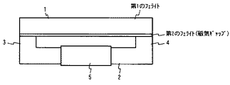
本発明の一実施例に係るフェライト磁心を、図1(a)、(b)に示す。このフェライト磁心は、キュリ−温度が異なるフェライトを一体焼成してなるものであって、フェライト磁心を主に構成する第1のフェライト部と、他の磁心と組み合わせた時、突き合わせ面となる外表面に配置され、磁気ギャップを構成する第2のフェライト部を一体的に形成したものである。図1(a)は、第2のフェライト部を第1のフェライト部の1面に形成するものであり、図1(b)は、第2のフェライト部を第1のフェライト部の対向する2面に形成するものである。
本発明の第1フェライト部に用いる第1のフェライト磁性材料は、キュリ−温度が100℃以上であるフェライト磁性材料であれば、特に限定されるものでは無い。電子部品用の磁心として要求される磁気特性(初透磁率、損失、品質係数等)に応じて、その組成は適宜選定され得るものである。
なお更にBi、V、Bなどの副成分を添加したり、ホウ珪酸ガラスなどのを加えて、1000℃以下の焼結を可能とした低温焼結磁性材料を第1のフェライト磁性材料として使用することが出来る。
例えば、Fe2O3、ZnO、MnOを主成分とし、Fe2O3:53mol%、ZnO:7mol%、MnO:40mol%と副成分として、前記主成分に対してCo3O4:0.2wt%添加したものであれば、その初透磁率μiは1900であり、キュリ−温度Tcは220℃である(A材)。
The present invention will be described in detail below.
1 (a) and 1 (b) show a ferrite magnetic core according to an embodiment of the present invention. This ferrite core is formed by integrally firing ferrites having different Curie temperatures, and the outer surface which becomes a butt surface when combined with the first ferrite portion mainly constituting the ferrite core and another magnetic core. And the second ferrite part constituting the magnetic gap is integrally formed. In FIG. 1A, the second ferrite part is formed on one surface of the first ferrite part. FIG. 1B shows the second ferrite part facing the first ferrite part. It is formed on the surface.
The first ferrite magnetic material used for the first ferrite part of the present invention is not particularly limited as long as it is a ferrite magnetic material having a Curie temperature of 100 ° C. or higher. The composition can be appropriately selected according to the magnetic properties (initial permeability, loss, quality factor, etc.) required for the magnetic core for the electronic component.
Furthermore, a low-temperature sintered magnetic material that can be sintered at 1000 ° C. or lower by adding subcomponents such as Bi, V, and B, or adding borosilicate glass or the like is used as the first ferrite magnetic material. I can do it.
For example, Fe 2 O 3 , ZnO, and MnO are the main components, Fe 2 O 3 : 53 mol%, ZnO: 7 mol%, MnO: 40 mol%, and subcomponents, Co 3 O 4 : 0. If 2 wt% is added, the initial permeability μi is 1900, and the Curie-temperature Tc is 220 ° C. (A material).
本発明の第2のフェライト部に用いる第2のフェライト磁性材料は、キュリ−温度が−40℃未満であるフェライト磁性材料であれば特に限定されるものでは無い。キュリ−温度TcはFe2O3やZnOの組成量によって変化することが知られており、前記第1のフェライト磁性材料との焼成収縮、収縮挙動のマッチングを考慮しながら、キュリ−温度を−40℃以下とするように、その組成を適宜決定すれば良い。
Mn−Zn系フェライト磁性材料とする場合には、主成分についてFe2O3を30〜40mol%、ZnOを35〜40mol%、残部MnOとするのが好ましい。例えば、Fe2O3:35mol%、ZnO:40mol%、MnO:25mol%のMn−Zn系フェライト磁性材料の場合には、キュリ−温度Tcは−50℃であり、通常電子部品が用いられる温度範囲−20℃〜+85℃では磁性を有さないものとなる(B材)。
他の第2のフェライト磁性材料として、Cu−Zn系フェライト磁性材料とする場合には、主成分についてFe2O3を40〜55mol%、ZnOを40mol%以上、残部CuOとするのが好ましい。例えば、Fe2O3:53mol%、ZnO:44mol%、CuO:3mol%のCu−Zn系フェライト磁性材料とすれば、そのキュリ−温度は−40℃未満となる(C材)。
なお更にBi、V、Bなどの副成分を添加したり、ホウ珪酸ガラスなどのを加えて、1000℃以下の焼結を可能とした低温焼結磁性材料を第2のフェライト磁性材料として使用することが出来る。
The second ferrite magnetic material used for the second ferrite portion of the present invention is not particularly limited as long as it is a ferrite magnetic material having a Curie temperature of less than −40 ° C. The Curie temperature Tc is known to change depending on the composition amount of Fe 2 O 3 and ZnO, and the Curie temperature is set while considering the matching of firing shrinkage and shrinkage behavior with the first ferrite magnetic material. What is necessary is just to determine the composition suitably so that it may be 40 degrees C or less.
When the Mn—Zn ferrite magnetic material is used, it is preferable that Fe 2 O 3 is 30 to 40 mol%, ZnO is 35 to 40 mol%, and the balance is MnO. For example, in the case of a Mn—Zn ferrite magnetic material of Fe 2 O 3 : 35 mol%, ZnO: 40 mol%, MnO: 25 mol%, the Curie temperature Tc is −50 ° C., and the temperature at which an electronic component is normally used. In the range of −20 ° C. to + 85 ° C., it has no magnetism (B material).
When the Cu—Zn ferrite magnetic material is used as the other second ferrite magnetic material, it is preferable that the main components are Fe 2 O 3 of 40 to 55 mol%, ZnO of 40 mol% or more, and the balance CuO. For example, when a Cu—Zn ferrite magnetic material of Fe 2 O 3 : 53 mol%, ZnO: 44 mol%, and CuO: 3 mol% is used, the Curie temperature is less than −40 ° C. (C material).
Further, a low-temperature sintered magnetic material that can be sintered at 1000 ° C. or lower by adding subcomponents such as Bi, V, and B or adding borosilicate glass or the like is used as the second ferrite magnetic material. I can do it.
図2に、先に例示した第1のフェライト磁性材料(A材)、及び第2のフェライト磁性材料(B材、C材)のTMAによる収縮特性を示す。比較例としてAl2O3の収縮特性もあわせて示す。Mn−Zn系、Cu−Zn系の第2のフェライト磁性材料の収縮挙動は、Al2O3の収縮挙動と大きく異なり、第1のフェライト磁性材料の挙動と近似している。第1のフェライト磁性材料の収縮開始温度、収縮率、及び1000℃から1100℃の間の収縮曲線の傾きは、Mn−Zn系フェライト 840℃、12.3%、−0.051であり、また、第2のフェライト磁性材料の収縮開始温度、収縮率、及び1000℃から1100℃の間の収縮曲線の傾きは、Mn−Zn系フェライト 765℃、14.3%、−0.038、Cu−Zn系 692℃、15.4%、−0.049であった。 In FIG. 2, the shrinkage | contraction characteristic by TMA of the 1st ferrite magnetic material (A material) illustrated previously and the 2nd ferrite magnetic material (B material, C material) is shown. As a comparative example, the shrinkage characteristics of Al 2 O 3 are also shown. The shrinkage behavior of the second ferrite magnetic material based on Mn—Zn and Cu—Zn is very different from the shrinkage behavior of Al 2 O 3 , and is similar to the behavior of the first ferrite magnetic material. The shrinkage onset temperature, shrinkage rate, and slope of the shrinkage curve between 1000 ° C. and 1100 ° C. of the first ferrite magnetic material are Mn—Zn ferrite 840 ° C., 12.3%, −0.051, and The shrinkage start temperature, shrinkage rate, and slope of the shrinkage curve between 1000 ° C. and 1100 ° C. of the second ferrite magnetic material are Mn—Zn ferrite 765 ° C., 14.3%, −0.038, Cu— Zn series was 692 ° C., 15.4%, and −0.049.
次に磁心の作製方法について説明する。
第1のフェライト磁性材料の作製手順を説明する。焼結後、前記組成となるように素原料を所定量秤量し、これに水及び分散剤を加えてアトライタ−にて混合して、乾燥後、大気中850℃で1.5時間仮焼し、この仮焼後の原料に水、分散剤を加えてアトライタ−で粉砕してスラリ−を作製した。これに、バインダ−を加えてスプレ−ドライヤ−で乾燥し、造粒粉とした。
Next, a method for manufacturing the magnetic core will be described.
A procedure for producing the first ferrite magnetic material will be described. After sintering, a predetermined amount of raw materials are weighed so as to have the above composition, water and a dispersing agent are added thereto, mixed with an attritor, dried, and calcined at 850 ° C. in the atmosphere for 1.5 hours. Then, water and a dispersant were added to the calcined raw material and pulverized with an attritor to prepare a slurry. A binder was added thereto and dried with a spray dryer to obtain granulated powder.
次に第2のフェライト磁性材料(Mn−Zn系、Cu−Zn系)の作製手順を説明する。焼結後、前記組成となるように素原料を所定量秤量し、これに水及び分散剤を加えてアトライタ−にて混合して、乾燥した後、大気中850℃で1.5時間仮焼した。仮焼後の原料に水、分散剤を加えてアトライタ−で粉砕し、乾燥して粉砕粉を作製した。粉砕粉にバインダ−としてPVB(ポリビニルブチラ−ル)、可塑剤としてBPBG(ブチルフタリルグリコ−ル酸ブチル)を添加し、エチルアルコ−ルを溶媒としてボ−ルミルにて混練してスラリ−とし、脱泡と粘度調整を行い、ドクタ−ブレ−ド法により150μm厚みのシ−ト状に形成した。シ−ト厚みは必要とされる磁気ギャップの間隔によって適宜形成され得る。 Next, a manufacturing procedure of the second ferrite magnetic material (Mn—Zn type, Cu—Zn type) will be described. After sintering, a predetermined amount of raw materials are weighed so as to have the above composition, water and a dispersant are added thereto, mixed with an attritor, dried, and then calcined at 850 ° C. in the atmosphere for 1.5 hours. did. Water and a dispersant were added to the calcined raw material, pulverized with an attritor, and dried to prepare pulverized powder. PVB (polyvinyl butyral) as a binder and BPBG (butyl butylphthalyl glycolate) as a plasticizer are added to the pulverized powder, and kneaded in a ball mill using ethyl alcohol as a solvent to form a slurry. Then, defoaming and viscosity adjustment were performed, and a sheet having a thickness of 150 μm was formed by a doctor blade method. The sheet thickness can be appropriately formed according to the required gap of the magnetic gap.
シートから所定形状に切り抜いたり、打ち抜いたりした第2のフェライト磁性材料からなるシートを前記金型内に配置し、さらにその上に第1のフェライト磁性材料の造粒粉を充填して、196MPaで圧縮成形して、第1のフェライト磁性材料・第2のフェライト磁性材料の順に積み重なった、I型の複合成形体とした。
A sheet made of a second ferrite magnetic material cut out or punched out from the sheet into a predetermined shape is placed in the mold, and further filled with granulated powder of the first ferrite magnetic material, and at 196 MPa. Compression molding was performed to obtain an I-type composite molded body in which the first ferrite magnetic material and the second ferrite magnetic material were stacked in this order .
得られた複合成形体を、酸素分圧が1〜2%に調整された焼成炉内で、焼成温度1300℃で5時間焼結して、第1、第2のフェライト磁性材料を接合して、第1のフェライト部の一面に第2のフェライト部(厚み0.15mm)を形成した、長さ30mm、幅5mm、厚み3mmのI型フェライト磁心を得た。
本発明においては、第2のフェライト磁性材料(B材、C材)の収縮開始温度を第1のフェライト磁性材料に対して−150℃〜+100℃の範囲に制御し、収縮カ−ブを同等(ほぼ同じ傾き)にすることで、焼結時の収縮差による応力を緩和しクラックや割れの無い磁心を作製することが出来た。さらに、第2のフェライト磁性材料で形成したシ−トを複数積み重ね、第2のフェライト部の厚みが、焼結後、1mmとなるように構成した。得られた磁心を切断し、顕微鏡で断面を観察したが、第1、第2のフェライト部にクラックなどの欠陥は観察されなかった。
比較例として第1のフェライト磁性材料と、厚みが150μmのAl2O3を用い、前記実施例と同様の方法で磁心を作製した。得られた磁心を長手方向に切断し、顕微鏡で断面を観察したところ、僅かではあるがAl2O3層から第1のフェライト磁性材料の層は至るクラックが発生していた。
The obtained composite molded body was sintered at a firing temperature of 1300 ° C. for 5 hours in a firing furnace in which the oxygen partial pressure was adjusted to 1 to 2%, and the first and second ferrite magnetic materials were joined. An I-type ferrite core having a length of 30 mm, a width of 5 mm, and a thickness of 3 mm, in which a second ferrite portion (thickness: 0.15 mm) was formed on one surface of the first ferrite portion, was obtained.
In the present invention, the shrinkage start temperature of the second ferrite magnetic material (material B, material C) is controlled in the range of −150 ° C. to + 100 ° C. with respect to the first ferrite magnetic material, and the shrinkage curve is equivalent. By using (substantially the same inclination), it was possible to relieve stress due to the shrinkage difference during sintering and to produce a magnetic core without cracks or cracks. Further, a plurality of sheets made of the second ferrite magnetic material were stacked, and the thickness of the second ferrite part was 1 mm after sintering. The obtained magnetic core was cut and the cross section was observed with a microscope, but no defects such as cracks were observed in the first and second ferrite portions.
As a comparative example, a magnetic core was produced in the same manner as in the above example using the first ferrite magnetic material and Al 2 O 3 having a thickness of 150 μm. When the obtained magnetic core was cut in the longitudinal direction and the cross section was observed with a microscope, cracks were generated from the Al 2 O 3 layer to the first ferrite magnetic material layer, albeit slightly.
次に、本発明の一実施例に係る磁心を用いて形成した電子部品(インダクタンス素子)について説明する。図3は、このインダクタンス素子の基本構造を示す外観図である。
実施例1と同様の手順にて得られた磁心(第2のフェライト磁性材料はMn−Zn系のB材を用いた)から、長さ30mm、幅5mm、厚み3mmのI字状フェライト磁心1を切り出した。ここで突き合わせ面側に位置する磁気ギャップの厚みは200μmとしている。さらに2つの磁脚3、4を繋ぐ連結部を備えたU字状磁心2を準備し、前記連接部6にコイルボビンを配置した。前記コイルボビン5には線径0.5mmφの線材が10回巻き回されている。前記I字状磁心1をU字状フェライト磁心2の磁脚3、4と実質的に空隙無く当接するように橋架けして配置して、樹脂粘着テ−プによりテ−ピング固定として本実施例に係るインダクタンス素子を構成した。なお、前記U字状フェライト磁心2は、2つの磁脚3、4を繋ぐ連結部が30mm、幅5mm、厚み3mmで、連結部からの立設する磁脚の高さが2.5mmであり、I字状フェライト磁心1を構成する第1のフェライト磁性材料を用いて形成されている。
Next, an electronic component (inductance element) formed using a magnetic core according to an embodiment of the present invention will be described. FIG. 3 is an external view showing the basic structure of this inductance element.
An I-shaped ferrite core 1 having a length of 30 mm, a width of 5 mm, and a thickness of 3 mm was obtained from a magnetic core obtained by the same procedure as in Example 1 (the second ferrite magnetic material was an Mn-Zn-based B material). Was cut out. Here, the thickness of the magnetic gap located on the abutting surface side is set to 200 μm. Further, a U-shaped
このインダクタンス素子の直流重畳特性を、室温状態で測定し評価したところ、磁気ギャップを設けないI字状フェライト磁心を用いた場合と比較し、優れた直流重畳特性を発揮することがわかった。第2のフェライト磁性材料と接合される第1のフェライト磁性材料の収縮率や収縮挙動を近似させることで、前記第2のフェライト磁性材料で構成される磁気ギャップの間隔を広く出来るため、電子部品が使用される電流範囲でインダクタンス値の変化が実質的にない、優れた直流重畳特性を得ることが出来た。 When the direct current superposition characteristics of this inductance element were measured and evaluated in a room temperature state, it was found that the direct current superposition characteristics were excellent as compared with the case where an I-shaped ferrite core without a magnetic gap was used. By approximating the contraction rate and contraction behavior of the first ferrite magnetic material to be joined to the second ferrite magnetic material, the gap of the magnetic gap composed of the second ferrite magnetic material can be widened. An excellent DC superposition characteristic with substantially no change in inductance value in the current range in which the current is used can be obtained.
本発明によれば、通常電子部品が用いられる温度範囲−20℃〜+85℃では磁性を有さない第2のフェライト磁性材料を用いて、磁気ギャップを構成する点である。この様に磁気ギャップを構成することで、スペ−サ−を設置する工程が簡素化でき、スペ−サ−設置によるインダクタンス値のばらつきを極めて小さくすることができる。また磁気ギャップが非磁性フェライトで形成されるため、磁気ギャップを一体形成した磁心を容易に得ることができるとともに、前記磁気ギャップが150μmを超える厚みであっても、クラック等の内部欠陥が生じない磁心を得ることが出来る。
また焼成収縮率、収縮挙動による内部残留応力を低減し、インダクタンス値のばらつきを抑えることが出来、長期的に電気的特性が安定し、組立が容易で直流重畳特性に優れた電子部品を得ることが出来る。
According to the present invention, the magnetic gap is formed by using the second ferrite magnetic material that does not have magnetism in a temperature range of −20 ° C. to + 85 ° C. in which an electronic component is normally used. By configuring the magnetic gap in this way, the process of installing the spacer can be simplified, and the variation in inductance value due to the installation of the spacer can be extremely reduced. Further, since the magnetic gap is formed of nonmagnetic ferrite, it is possible to easily obtain a magnetic core in which the magnetic gap is integrally formed, and internal defects such as cracks do not occur even if the magnetic gap has a thickness exceeding 150 μm. A magnetic core can be obtained.
In addition, the internal residual stress due to firing shrinkage and shrinkage behavior can be reduced, variation in inductance value can be suppressed, electrical characteristics can be stabilized over the long term, easy assembly, and excellent electronic superimposition characteristics can be obtained. I can do it.
1 I字状磁心
2 U字状磁心
3、4 磁脚
5 コイルボビン
6 連接部
1 I-shaped
Claims (1)
前記突合せフェライト磁心は、造粒粉からなるキュリ−温度が100℃以上の第1のフェライト磁性材料と、前記突合せ面側に、シート状のキュリ−温度が−40℃未満の第2のフェライト磁性材料を一体的に成形し、
しかる後、一体焼結して、前記第1のフェライト磁性材料からなる第1のフェライト部と、前記第2のフェライト磁性材料からなる第2のフェライト部を接合してなり、少なくとも、前記脚付フェライト磁心との突き合わせ面に前記第2のフェライト磁性材料で構成された磁気ギャップが形成されていることを特徴とする特徴とする電子部品。
A legged ferrite core, a ferrite core that abuts the legged ferrite core, and a winding disposed on the legged ferrite core and / or the butt ferrite core,
The butt ferrite core includes a first ferrite magnetic material having a Curie temperature of 100 ° C. or more made of granulated powder, and a second ferrite magnet having a sheet-like Curie temperature of less than −40 ° C. on the butt surface side. The material is molded integrally,
Thereafter, the first ferrite part made of the first ferrite magnetic material and the second ferrite part made of the second ferrite magnetic material are joined together, and at least the legs are attached. An electronic component characterized in that a magnetic gap made of the second ferrite magnetic material is formed on a butt surface with a ferrite magnetic core.
Priority Applications (1)
| Application Number | Priority Date | Filing Date | Title |
|---|---|---|---|
| JP2005091519A JP5158829B2 (en) | 2005-03-28 | 2005-03-28 | Electronic components |
Applications Claiming Priority (1)
| Application Number | Priority Date | Filing Date | Title |
|---|---|---|---|
| JP2005091519A JP5158829B2 (en) | 2005-03-28 | 2005-03-28 | Electronic components |
Publications (3)
| Publication Number | Publication Date |
|---|---|
| JP2006278432A JP2006278432A (en) | 2006-10-12 |
| JP2006278432A5 JP2006278432A5 (en) | 2008-04-03 |
| JP5158829B2 true JP5158829B2 (en) | 2013-03-06 |
Family
ID=37212918
Family Applications (1)
| Application Number | Title | Priority Date | Filing Date |
|---|---|---|---|
| JP2005091519A Active JP5158829B2 (en) | 2005-03-28 | 2005-03-28 | Electronic components |
Country Status (1)
| Country | Link |
|---|---|
| JP (1) | JP5158829B2 (en) |
Families Citing this family (1)
| Publication number | Priority date | Publication date | Assignee | Title |
|---|---|---|---|---|
| CN103208352B (en) * | 2013-03-15 | 2016-08-10 | 沈阳工业大学 | There is the power transformer of D.C. magnetic biasing suppression function based on magnetic temp compensating |
Family Cites Families (5)
| Publication number | Priority date | Publication date | Assignee | Title |
|---|---|---|---|---|
| JPH0855713A (en) * | 1994-08-16 | 1996-02-27 | Sony Corp | Manufacture of composite magnetic material |
| JPH09110520A (en) * | 1995-10-20 | 1997-04-28 | Hitachi Metals Ltd | Ferrite sintered compact |
| JPH11345715A (en) * | 1998-06-02 | 1999-12-14 | Kijima:Kk | Miniaturized electric winding parts |
| US7295092B2 (en) * | 2002-12-19 | 2007-11-13 | Cooper Technologies Company | Gapped core structure for magnetic components |
| JP4362807B2 (en) * | 2003-02-27 | 2009-11-11 | 日立金属株式会社 | Ceramic composite material |
-
2005
- 2005-03-28 JP JP2005091519A patent/JP5158829B2/en active Active
Also Published As
| Publication number | Publication date |
|---|---|
| JP2006278432A (en) | 2006-10-12 |
Similar Documents
| Publication | Publication Date | Title |
|---|---|---|
| JP5212623B2 (en) | Ni-Zn-Cu ferrite powder, green sheet containing the Ni-Zn-Cu ferrite powder, and Ni-Zn-Cu ferrite sintered body. | |
| EP1661869B1 (en) | Ferrite material and electronic component using same | |
| JP2008130736A (en) | Electronic component and its manufacturing method | |
| US10679788B2 (en) | Method of manufacturing magnetic core elements | |
| US7892446B2 (en) | Ferrite material | |
| JP5515195B2 (en) | Ni-Zn ferrite powder, green sheet containing the Ni-Zn ferrite powder, and Ni-Zn ferrite sintered body. | |
| JP4362807B2 (en) | Ceramic composite material | |
| JP4524751B2 (en) | Magnetic core and electronic component using the same | |
| JP5158829B2 (en) | Electronic components | |
| JP6397606B2 (en) | Magnetic material, magnetic porcelain composition, ferrite magnet and method for producing magnetic porcelain composition | |
| JP4822385B2 (en) | Ferrite material and inductance element | |
| JP2006344683A (en) | Drum core and inductor | |
| JP4761187B2 (en) | Magnetic oxide material | |
| JP2006210493A (en) | Antenna coil and transponder | |
| JP4384346B2 (en) | Ni-Cu-Zn ferrite magnetic material | |
| JP2599887B2 (en) | Magnetic materials for chip parts | |
| JP4654559B2 (en) | Ferrite magnetic material and ferrite core | |
| US20020148995A1 (en) | Oxide magnetic material and coil part using the same | |
| JP5717056B2 (en) | Ferrite porcelain manufacturing method | |
| JP2008109415A (en) | Antenna | |
| JP3678479B2 (en) | Low temperature coefficient ferrite core and electronic components | |
| JPH0812476A (en) | Method for sintering oxide magnetic material with high magnetic permeability | |
| JP6574574B2 (en) | Multilayer inductor | |
| JP4433914B2 (en) | Sintered body and coil component using the same | |
| KR20230063544A (en) | Method for manufacturing magnetic core for transformer, air gap composition for the magnetic core and the magnetic core with air gap |
Legal Events
| Date | Code | Title | Description |
|---|---|---|---|
| A621 | Written request for application examination |
Free format text: JAPANESE INTERMEDIATE CODE: A621 Effective date: 20080214 |
|
| A521 | Request for written amendment filed |
Free format text: JAPANESE INTERMEDIATE CODE: A523 Effective date: 20080215 |
|
| A977 | Report on retrieval |
Free format text: JAPANESE INTERMEDIATE CODE: A971007 Effective date: 20100716 |
|
| A131 | Notification of reasons for refusal |
Free format text: JAPANESE INTERMEDIATE CODE: A131 Effective date: 20100723 |
|
| A521 | Request for written amendment filed |
Free format text: JAPANESE INTERMEDIATE CODE: A523 Effective date: 20100916 |
|
| A02 | Decision of refusal |
Free format text: JAPANESE INTERMEDIATE CODE: A02 Effective date: 20110624 |
|
| A61 | First payment of annual fees (during grant procedure) |
Free format text: JAPANESE INTERMEDIATE CODE: A61 Effective date: 20121207 |
|
| R150 | Certificate of patent or registration of utility model |
Ref document number: 5158829 Country of ref document: JP Free format text: JAPANESE INTERMEDIATE CODE: R150 Free format text: JAPANESE INTERMEDIATE CODE: R150 |
|
| FPAY | Renewal fee payment (event date is renewal date of database) |
Free format text: PAYMENT UNTIL: 20151221 Year of fee payment: 3 |
|
| S531 | Written request for registration of change of domicile |
Free format text: JAPANESE INTERMEDIATE CODE: R313531 |
|
| S533 | Written request for registration of change of name |
Free format text: JAPANESE INTERMEDIATE CODE: R313533 |
|
| R350 | Written notification of registration of transfer |
Free format text: JAPANESE INTERMEDIATE CODE: R350 |