JP5154315B2 - Liquid crystal display panel and electronic device - Google Patents
Liquid crystal display panel and electronic device Download PDFInfo
- Publication number
- JP5154315B2 JP5154315B2 JP2008166916A JP2008166916A JP5154315B2 JP 5154315 B2 JP5154315 B2 JP 5154315B2 JP 2008166916 A JP2008166916 A JP 2008166916A JP 2008166916 A JP2008166916 A JP 2008166916A JP 5154315 B2 JP5154315 B2 JP 5154315B2
- Authority
- JP
- Japan
- Prior art keywords
- liquid crystal
- shielding film
- color filter
- light shielding
- display panel
- Prior art date
- Legal status (The legal status is an assumption and is not a legal conclusion. Google has not performed a legal analysis and makes no representation as to the accuracy of the status listed.)
- Active
Links
- 239000004973 liquid crystal related substance Substances 0.000 title claims description 76
- 239000000758 substrate Substances 0.000 claims description 82
- 125000006850 spacer group Chemical group 0.000 claims description 43
- 239000011347 resin Substances 0.000 claims description 17
- 229920005989 resin Polymers 0.000 claims description 17
- 239000003566 sealing material Substances 0.000 claims description 7
- 230000005684 electric field Effects 0.000 claims description 6
- 239000000463 material Substances 0.000 claims description 4
- 239000000565 sealant Substances 0.000 claims description 2
- 238000005192 partition Methods 0.000 claims 1
- 239000007787 solid Substances 0.000 description 9
- 229910052751 metal Inorganic materials 0.000 description 8
- 239000002184 metal Substances 0.000 description 8
- VYZAMTAEIAYCRO-UHFFFAOYSA-N Chromium Chemical compound [Cr] VYZAMTAEIAYCRO-UHFFFAOYSA-N 0.000 description 5
- 239000012535 impurity Substances 0.000 description 5
- 238000004519 manufacturing process Methods 0.000 description 4
- 239000004065 semiconductor Substances 0.000 description 4
- 229910052804 chromium Inorganic materials 0.000 description 3
- 239000011651 chromium Substances 0.000 description 3
- 238000010586 diagram Methods 0.000 description 3
- 239000011521 glass Substances 0.000 description 3
- 239000011159 matrix material Substances 0.000 description 3
- 230000004048 modification Effects 0.000 description 3
- 238000012986 modification Methods 0.000 description 3
- 230000001681 protective effect Effects 0.000 description 3
- 239000004925 Acrylic resin Substances 0.000 description 2
- 229920000178 Acrylic resin Polymers 0.000 description 2
- 229910052581 Si3N4 Inorganic materials 0.000 description 2
- 229910021417 amorphous silicon Inorganic materials 0.000 description 2
- 230000000694 effects Effects 0.000 description 2
- HQVNEWCFYHHQES-UHFFFAOYSA-N silicon nitride Chemical compound N12[Si]34N5[Si]62N3[Si]51N64 HQVNEWCFYHHQES-UHFFFAOYSA-N 0.000 description 2
- VYPSYNLAJGMNEJ-UHFFFAOYSA-N Silicium dioxide Chemical compound O=[Si]=O VYPSYNLAJGMNEJ-UHFFFAOYSA-N 0.000 description 1
- 230000015572 biosynthetic process Effects 0.000 description 1
- 230000001413 cellular effect Effects 0.000 description 1
- 230000006866 deterioration Effects 0.000 description 1
- 238000010828 elution Methods 0.000 description 1
- 230000002093 peripheral effect Effects 0.000 description 1
- 229920002120 photoresistant polymer Polymers 0.000 description 1
- 229910052814 silicon oxide Inorganic materials 0.000 description 1
- 238000000638 solvent extraction Methods 0.000 description 1
Images


Description
本発明は、表示ムラのない安定した表示品質を達成し得る液晶表示パネル及びこの液晶表示パネルを使用した電子機器に関する。 The present invention relates to an electronic device using the liquid crystal display panel of the liquid crystal display panel及Biko capable of achieving stable display quality without display unevenness.
液晶表示パネルは、アレイ基板と、このアレイ基板と対向するように設けられたカラーフィルタ基板と、アレイ基板及びカラーフィルタ基板の間に封入された液晶層とを備えている。アレイ基板は、マトリクス状に配置された複数の走査線及び信号線と、走査線及び信号線により区画されるそれぞれの位置に形成された画素電極とを備えている。また、カラーフィルタ基板は、アレイ基板の各画素電極に対応する位置に所定色のカラーフィルタ層が配置されると共に、各画素電極に対応する位置を除いて遮光膜が形成されている。この遮光膜は、直接画像表示に関与しない位置を遮光し、各画素の輪郭をはっきりさせ、コントラストを向上させる役目を有するものである。この従来例のカラーフィルタ基板の構成を概略断面図である図7を用いて説明する。 The liquid crystal display panel includes an array substrate, a color filter substrate provided so as to face the array substrate, and a liquid crystal layer sealed between the array substrate and the color filter substrate. The array substrate includes a plurality of scanning lines and signal lines arranged in a matrix, and pixel electrodes formed at respective positions partitioned by the scanning lines and signal lines. In the color filter substrate, a color filter layer of a predetermined color is disposed at a position corresponding to each pixel electrode of the array substrate, and a light shielding film is formed except for a position corresponding to each pixel electrode. This light-shielding film shields positions that are not directly involved in image display, has the role of clarifying the outline of each pixel and improving contrast. The configuration of this conventional color filter substrate will be described with reference to FIG. 7 which is a schematic sectional view.
従来の液晶表示パネルのカラーフィルタ基板CFbは、ガラス基板等の透明基板31の表面に遮光膜が形成されているが、この遮光膜のパターンは表示領域33及び非表示領域34のそれぞれで異なっている。すなわち、表示領域33の遮光膜BMdは図示しないアレイ基板の走査線及び信号線に対応する位置にマトリクス状に形成されており、非表示領域34の遮光膜BMnは表示領域33の遮光膜BMdの周囲を囲むようにベタ状に形成されている(下記特許文献1参照)。これらの遮光膜BMd及びBMnとしては、クロム金属等からなる金属製の遮光膜や樹脂製の遮光膜が用いられるが、以下においては樹脂製の遮光膜を使用した場合について説明する。なお、一般的に使用されている樹脂製の遮光膜の厚さは1〜2μm程度であり、金属製の遮光膜の厚さは0.1〜0.2μm程度である。
A color filter substrate CFb of a conventional liquid crystal display panel has a light shielding film formed on the surface of a
表示領域33の遮光膜BMdの間及び表面にはそれぞれの画素毎に所定の色、例えば赤(R)、緑(G)、青(B)のカラーフィルタ層32が形成されている。なお図7ではストライプ状に形成されている各色のカラーフィルタ層における、特定の色の方向に沿った断面を示している。
A
なお、カラーフィルタ層32は、一般的に表示領域33と非表示領域34との境界近傍まで形成されている。それは、この領域で構成が異なると、境界近傍に大きな段差が生じ、この段差により液晶分子の配向に乱れが生じる恐れがあるからである。
The
そして、カラーフィルタ層32の表面及び非表示領域34の遮光膜BMnの表面には透明な例えばアクリル樹脂等からなるオーバーコート層35が形成されている。このオーバーコート層35は、カラーフィルタ基板CFbの表面の凹凸を緩和し、カラーフィルタ層32、樹脂製の遮光膜BMd,BMnを保護して、液晶層と直接接触するのを防ぐために設けられている。
A
そして、表示領域33の遮光膜BMdに対応する位置、及び非表示領域34のシール材50より内側において、所定の高さの柱状スペーサ38が形成されている。なお、この柱状スペーサ38は、表面に感光性樹脂層を形成した後、露光・現像することにより形成される。そしてこの柱状スペーサ38はその製造方法からして「フォトスペーサ」とも称される。
A
ところで、上記のようなカラーフィルタ基板CFbは、図7に示されているように、透明基板31から柱状スペーサ38までの高さが、表示領域33と非表示領域34とで異なるという問題が発生する。この理由については、モノクロ液晶表示装置に関する特許文献1の段落番号「0007」にも記載されているが、表示領域33における幅の狭い遮光膜BMdと、非表示領域34におけるベタ状に形成されている遮光膜BMnとで、その上に形成される層の厚さに差が生じるためである。
Incidentally, the color filter substrate CFb as described above has a problem that the height from the
つまり表示領域33の遮光膜BMdの上に形成されるカラーフィルタ層32に比べ、非表示領域34の遮光膜BMnの上に形成されるカラーフィルタ層32の方が厚く形成されてしまう。そして厚さの異なるカラーフィルタ層32の上に最終的に形成される柱状スペーサ38までもがその影響を受けてしまうため、透明基板31の表面から柱状スペーサ38の上部までの高さが、表示領域33と、非表示領域34とで異なってしまうことになる。
That is, the
このように、いわゆる柱状スペーサ38の高さが、表示領域33と非表示領域34とで異なってしまうと、カラーフィルタ基板CFbとアレイ基板とをシール材50により貼り合わせて液晶表示パネルを形成した際に、表示領域33と非表示領域34の境界付近でセルギャップの差に起因する表示ムラが生じてしまう。このような表示ムラは特にセルギャップの差異に敏感なモードの液晶表示パネルでは顕著となる。
As described above, when the so-called
なお、上記特許文献2には、非表示領域34のカラーフィルタ層32の厚さを薄くし、表示領域33のカラーフィルタ層32の厚さと非表示領域34のベタ状の遮光膜BMn及びカラーフィルタ層32の合計厚さとが同じになるようにした液晶表示パネルが開示されている。しかしながら、通常は表示領域33のカラーフィルタ層32及び非表示領域34のカラーフィルタ層32はそれぞれの色毎に同時に作製されるため、非表示領域34のカラーフィルタ層32の厚さを表示領域33のカラーフィルタ層32の厚さよりも薄くするには別途特殊な製造工程が必要となる。そのため、液晶表示パネルの製造効率を上げるためには上記特許文献2に示されている発明の構成は採用し難いという問題がある。
In Patent Document 2, the thickness of the
本発明は、上記課題の少なくとも一部を解決するためになされたものであり、以下の形態又は適用例として実現することが可能である。 SUMMARY An advantage of some aspects of the invention is to solve at least a part of the problems described above, and the invention can be implemented as the following forms or application examples.
[適用例1]本適用例に係る液晶表示パネルは、第1の基板及び第2の基板と、第1の基板と第2の基板とがシール材を介して貼り合わされた隙間に封入された液晶と、複数の画素を有する表示領域と、表示領域の周囲に位置して、シール材が配置される非表示領域と、を有する液晶表示パネルであって、第2の基板は、複数の画素を区画する第1の遮光膜と、複数の画素に対応して設けられたカラーフィルタ層と、非表示領域に設けられた第2の遮光膜と、を備え、表示領域には、第1の遮光膜に対応する位置に第1の柱状スペーサが配置されており、非表示領域は、第2の遮光膜の表面にカラーフィルタ層が形成された内側領域と、内側領域よりも外側であって、シール材よりも内側に第2の柱状スペーサが配置された外側領域と、を有する。 Application Example 1 A liquid crystal display panel according to this application example is sealed in a gap in which a first substrate and a second substrate, and the first substrate and the second substrate are bonded to each other through a sealant. a liquid crystal, a display area having a plurality of pixels, located around the table display region, a liquid crystal display panel having a non-display region sheet Lumpur material is arranged, a second substrate, comprises a first light shielding film for partitioning the pixels of multiple, and a color filter layer provided in correspondence to the pixels of multiple, a second light-shielding film provided on the non-display area, a table display region the, at a position corresponding to the first light shielding film and the first columnar spacer is arranged, the non-display area, an inner area color filter layer is formed on the surface of the second light-shielding film, the inner an outer than the side regions, have a, and an outer region where the second column spacer is arranged on the inner side of the sheet Lumpur material That.
この構成によれば、第2の基板の非表示領域は、ベタ状の第2の遮光膜の表面にカラーフィルタ層が形成された内側領域と、ベタ状の第2の遮光膜の表面に第2の柱状スペーサが配置された外側領域とを有する。つまり、非表示領域における内側領域には、カラーフィルタ層が形成されているが、柱状スペーサは形成されていない。逆に、外側領域には、第2の柱状スペーサが形成されているが、カラーフィルタ層は形成されていない。 According to this configuration, the non-display area of the second substrate includes the inner area where the color filter layer is formed on the surface of the solid second light shielding film and the surface of the solid second light shielding film. And an outer region in which two columnar spacers are arranged. That is, the color filter layer is formed in the inner region in the non-display region, but the columnar spacer is not formed. On the contrary, the second columnar spacer is formed in the outer region, but the color filter layer is not formed.
一般的に、液晶表示パネルの第2の基板におけるカラーフィルタ層は、表示領域及び非表示領域共にそれぞれの色毎に同時に作製されているが、表示領域の第1の遮光膜は細かく区画されているのに対して非表示領域の第2の遮光膜はベタ状であるため、非表示領域のカラーフィルタ層の厚さは表示領域のカラーフィルタ層の厚さよりも厚くなってしまう。そのため、非表示領域のカラーフィルタ層に対応する位置に柱状スペーサを形成すると、この柱状スペーサの相対的高さ(カラーフィルタ基板の表面から柱状スペーサの上部までの高さ)は表示領域の第1の遮光膜に対応する位置に形成された第1の柱状スペーサの相対的高さよりも高くなってしまう。 In general, the color filter layer in the second substrate of the liquid crystal display panel is formed simultaneously for each color in both the display area and the non-display area, but the first light shielding film in the display area is finely partitioned. On the other hand, since the second light-shielding film in the non-display area is solid, the thickness of the color filter layer in the non-display area is larger than the thickness of the color filter layer in the display area. Therefore, when a columnar spacer is formed at a position corresponding to the color filter layer in the non-display area, the relative height of the columnar spacer (the height from the surface of the color filter substrate to the top of the columnar spacer) is the first in the display area. It becomes higher than the relative height of the first columnar spacer formed at the position corresponding to the light shielding film.
本適用例の液晶表示パネルによれば、カラーフィルタ層が存在していない外側領域に第2の柱状スペーサが配置されているので、カラーフィルタ層に起因する柱状スペーサの高さの差を抑えることが可能となり、基板間のギャップを確保すると共に表示領域と非表示領域との境界付近で生じる表示ムラを防ぐことができる。したがって、カラーフィルタ層の層厚を調整するなど別途特殊な製造工程を有さずとも、表示領域のセルギャップが均一となるようにすることができ、表示ムラのない安定した均一な表示品質を達成し得る液晶表示パネルとなる。 According to the liquid crystal display panel of the present application example, since the second columnar spacers outside the region where the color filter layer is not present is arranged to suppress the difference in height of the columnar spacers due to the color filter layer This makes it possible to secure a gap between the substrates and prevent display unevenness that occurs near the boundary between the display area and the non-display area. Therefore, the cell gap in the display area can be made uniform without special manufacturing processes such as adjusting the layer thickness of the color filter layer, and stable and uniform display quality without display unevenness can be achieved. a liquid crystal display panel that can be achieved.
[適用例2]上記適用例に係る液晶表示パネルにおいて、第1の遮光膜及び第2の遮光膜は、樹脂製であることが好ましい。 Application Example 2 A liquid crystal display panel according to the application example described above, the first shielding Maku及beauty second light shielding film is preferably made of resin.
この構成によれば、一般的に使用されている樹脂製の遮光膜の厚さは例えば1〜2μm程度であり、クロム等の金属製の遮光膜の厚さは例えば0.1〜0.2μm程度である。そのため、非表示領域のカラーフィルタ層の厚さが表示領域のカラーフィルタ層の厚さよりも厚くなる現象は、樹脂製の遮光膜(第1の遮光膜、第2の遮光膜)の方が金属製の遮光膜の場合よりも大きく現れる。従って、係る態様の液晶表示パネルによれば、特に効果が顕著に表れる。 According to this configuration, the thickness of a commonly used resin light shielding film is, for example, about 1 to 2 μm, and the thickness of a metal light shielding film such as chromium is, for example, 0.1 to 0.2 μm. Degree. Therefore, the phenomenon that the thickness of the color filter layer in the non-display area becomes thicker than the thickness of the color filter layer in the display area is that the resin-made light shielding film (first light shielding film, second light shielding film) is more metallic. It appears larger than in the case of a light-shielding film. Therefore, according to the liquid crystal display panel of this aspect, the effect is particularly remarkable.
[適用例3]上記適用例に係る液晶表示パネルにおいて、カラーフィルタ層の表面、及び、カラーフィルタ層が重畳されない第2の遮光膜の表面に、オーバーコート層が形成されていることが好ましい。 Application Example 3 A liquid crystal display panel according to the application example described above, the surface of the color filter layer, and the surface of the second light-shielding film color filter layer is not such is superimposed, an overcoat layer is formed It is preferable.
この構成によれば、カラーフィルタ層及び樹脂製の遮光膜からは液晶内に不純物の溶出の可能性があるが、カラーフィルタ層の表面(カラーフィルタ層と第1の柱状スペーサとの間を含む)、カラーフィルタ層が重畳されない第2の遮光膜の表面(第2の遮光膜と第2の柱状スペーサとの間を含む)にオーバーコート層を形成したので、液晶内への不純物の溶出を防止して液晶の劣化を抑制することができる。加えて、オーバーコート層は例えば透明樹脂層から形成されるが、このオーバーコート層形成時に表面の凹凸が平坦化されるため、セルギャップがより均一化され、より均一な表示品質を達成し得る液晶表示パネルが得られる。 According to this configuration, the color filter layer and the resin light-shielding film may cause impurities to elute into the liquid crystal, but the surface of the color filter layer (including between the color filter layer and the first columnar spacer). ) Since the overcoat layer is formed on the surface of the second light-shielding film (including the space between the second light-shielding film and the second columnar spacer) on which the color filter layer is not superimposed, the impurities are eluted into the liquid crystal. This can prevent the deterioration of the liquid crystal. In addition, the overcoat layer is formed of, for example, a transparent resin layer. Since the surface unevenness is flattened when the overcoat layer is formed, the cell gap can be made more uniform and more uniform display quality can be achieved. A liquid crystal display panel is obtained.
[適用例4]上記適用例に係る液晶表示パネルにおいて、第1の基板は、第1電極及び第2電極を有し、第1電極と第2電極との間に生じる横方向電界により液晶が駆動されることが好ましい。 Application Example 4 In the liquid crystal display panel according to the application example described above, the first substrate has a first electrode and a second electrode, Ri by the lateral electric field generated between the first electrode and the second electrode it is preferred that the liquid crystal is driven.
この構成によれば、種々の方式の液晶表示パネルに対しても適用可能であるが、FFSモードないしIPSモード等の横方向電界方式の液晶表示パネルの表示画質はセルギャップに対して敏感であるため、特に横方向電界方式の液晶表示パネルに適用すると効果が顕著に表れる。 According to this configuration, the present invention can be applied to various types of liquid crystal display panels, but the display image quality of a liquid crystal display panel of a horizontal electric field type such as an FFS mode or an IPS mode is sensitive to a cell gap. Therefore, the effect is particularly remarkable when applied to a liquid crystal display panel of a horizontal electric field type.
[適用例5]本適用例に係る電子機器は、上記した液晶表示パネルを備えていることを特徴とする。
Application Example 5 An electronic apparatus according to this application example is characterized in that it comprises a liquid crystal display panel described above.
この構成によれば、表示ムラが少なく安定した表示品質を有する電子機器が得られる。 According to this configuration, an electronic apparatus having stable display quality with little display unevenness can be obtained.
以下、本発明を実施するための最良の形態について、実施例及び図面を参照しながら詳細に説明する。ただし、以下に示す実施例は、本発明の技術思想を具体化するためにFFSモード(横方向電界方式)の液晶表示パネルを例にとって説明するものであって、本発明をこの実施例に記載されたFFSモードの液晶表示パネルに特定することを意図するものではなく、本発明は特許請求の範囲に含まれるその他の実施形態のものにも等しく適応し得るものである。なお、以下においては上述した従来例の液晶表示パネルのカラーフィルタ基板CFbと同一の構成部分には同一の参照符号を付与して説明することとする。 Hereinafter, the best mode for carrying out the present invention will be described in detail with reference to examples and drawings. However, in the following embodiment, an FFS mode (transverse electric field type) liquid crystal display panel will be described as an example in order to embody the technical idea of the present invention, and the present invention will be described in this embodiment. The present invention is not intended to be specific to an FFS mode liquid crystal display panel, and the present invention is equally applicable to other embodiments within the scope of the claims. In the following description, the same components as those of the color filter substrate CFb of the above-described conventional liquid crystal display panel are given the same reference numerals.
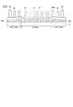
なお、図1は実施例のFFSモードの液晶表示パネルのカラーフィルタ基板の模式平面図である。図2は図1のA部分のカラーフィルタ基板を透視して表した2画素分の概略平面図である。図3は図2のC−C線に沿った断面図である。図4は図2のE−E線に沿った断面図である。図5は図1のF−F線に沿った拡大断面図である。図6(a)は液晶表示パネルを搭載したパーソナルコンピュータを示す図であり、図6(b)は液晶表示パネルを搭載した携帯電話機を示す図である。 FIG. 1 is a schematic plan view of a color filter substrate of the FFS mode liquid crystal display panel of the embodiment. FIG. 2 is a schematic plan view of two pixels represented by seeing through the color filter substrate of portion A in FIG. 3 is a cross-sectional view taken along the line CC of FIG. 4 is a cross-sectional view taken along line EE in FIG. FIG. 5 is an enlarged sectional view taken along line FF in FIG. FIG. 6A is a diagram showing a personal computer equipped with a liquid crystal display panel, and FIG. 6B is a diagram showing a mobile phone equipped with a liquid crystal display panel.
実施例のFFSモードの液晶表示パネル10の構成を図3(図1〜図4)を主体に説明する。この実施例のFFSモードの液晶表示パネル10の第1の基板としてのアレイ基板ARは、ガラス基板等の透明基板11の表面に例えばMo/Alの2層配線からなる複数の走査線12及び複数のコモン配線13が互いに平行になるように形成されている(図2参照)。また、走査線12及びコモン配線13で囲まれたそれぞれの領域に例えばITOからなる第1電極としての下電極14が形成されている。この下電極14は、コモン配線13とは電気的に接続されているが、走査線12ないしゲート電極Gとは接続されておらず、共通電極として作用する。
The configuration of the FFS mode liquid
また、この走査線12、コモン配線13及び下電極14が形成された透明基板11の表面全体に亘って窒化硅素層ないしは酸化硅素層からなるゲート絶縁膜15が被覆されている。更に、このゲート絶縁膜15の表面のTFT形成領域にはアモルファス・シリコン(以下「a−Si」という。)層からなる半導体層16が形成されている。この半導体層16が形成されている位置の走査線12の領域がTFTのゲート電極Gを形成する(図2、図3参照)。
A
また、例えばMo/Al/Moの3層構造の導電性層からなるソース電極Sを含む信号線17及びドレイン電極Dが形成されている。この信号線17のソース電極S部分及びドレイン電極D部分は、いずれも半導体層16の表面に部分的に重なっている(図2、図3参照)。更に、透明基板11の表面全体に窒化硅素層からなる保護絶縁膜18が被覆されており、ドレイン電極Dに対応する位置の保護絶縁膜18にコンタクトホール19が形成されている。
Further, a
そして、図2に示したパターンとなるように、走査線12及び信号線17で囲まれた領域の保護絶縁膜18上にスリット20を有する例えばITOからなる第2電極としての上電極21が形成されている。この上電極21はコンタクトホール19を介してドレイン電極Dと電気的に接続されており、画素電極として作用する。更に、この表面全体に亘り所定の配向膜(図示せず)が形成されている。
Then, an
一方、第2の基板としてのカラーフィルタ基板CFaはガラス基板等の透明基板31の表面に樹脂製の遮光膜BMd(第1の遮光膜)、BMn(第2の遮光膜)が形成されている。この遮光膜BMd,BMnは、上述の従来例のカラーフィルタ基板CFbの場合と同様に、表示領域33及び非表示領域34で異なるパターンに形成されている(図1、図5参照)。すなわち、表示領域33の遮光膜BMdはアレイ基板ARの走査線12及び信号線17に対応する位置にマトリクス状に形成されており、非表示領域34の遮光膜BMnは表示領域33の遮光膜BMdの周囲を囲むようにベタ状に形成されている(図5参照)。なお、表示領域33の遮光膜BMdと非表示領域34の遮光膜BMnとは、例えば透明基板31の表面に遮光性材料が混入されたフォトレジスト層を形成した後、露光後に現像処理することにより同時に形成されるため、同じ高さ(図5参照)に形成される。
On the other hand, the color filter substrate CFa as the second substrate has a resin light shielding film BMd (first light shielding film) and BMn (second light shielding film) formed on the surface of the
なお、樹脂製の遮光膜BMd,BMnは、本実施例のようなFFSモードの液晶表示パネルや、IPSモードの液晶表示パネルのように、アレイ基板側に画素電極及び共通電極が形成されるタイプの液晶表示パネルにおいては特に好ましい。なぜならば、カラーフィルタ基板側に金属製の遮光膜を形成すると、この金属製の遮光膜とアレイ側基板との間で予期せぬ電界が発生してしまい、液晶分子に影響を与える恐れがあるが、樹脂製の遮光膜BMd,BMnであればそのような恐れが生じないためである。 The light shielding films BMd and BMn made of resin are a type in which a pixel electrode and a common electrode are formed on the array substrate side like the FFS mode liquid crystal display panel and the IPS mode liquid crystal display panel as in this embodiment. This is particularly preferable in the liquid crystal display panel. This is because if a metal light-shielding film is formed on the color filter substrate side, an unexpected electric field is generated between the metal light-shielding film and the array-side substrate, which may affect liquid crystal molecules. However, such a fear does not occur if the light shielding films BMd and BMn are made of resin.
また、図5に示すように、表示領域33の遮光膜BMdの間及び表面にはそれぞれの画素毎に所定の色、例えば赤(R)、緑(G)、青(B)のカラーフィルタ層32が所定の厚さで形成されている。また、非表示領域34は、表示領域33側の内側領域34iと、この内側領域34iの外周側に位置する外側領域34oとからなっている。非表示領域34の内側領域34iには、ベタ状の遮光膜BMnの表面に表示領域33側に沿ってカラーフィルタ層32が形成されている。
Further, as shown in FIG. 5, a color filter layer of a predetermined color, for example, red (R), green (G), or blue (B), is provided for each pixel between and on the surface of the light shielding film BMd of the
この非表示領域34の内側領域34iに形成されたカラーフィルタ層32の厚さは、従来例について既に述べたのと同様の理由で、表示領域33の遮光膜BMd上に形成されたカラーフィルタ層32の厚さよりも厚くなる。なお、非表示領域34の外側領域34oにはベタ状の遮光膜BMnの表面にカラーフィルタ層は形成されていない。また、非表示領域34においてカラーフィルタ層32が形成されている内側領域34iは、図1に示したように、2画素分程度の領域、或いは3画素分程度の領域が好ましい。この領域があまり広く(例えば10画素分程度の領域)まで広くなってしまうと、後述するようにこの内側領域34iには柱状スペーサを形成しないため(図1参照)、この領域では対向する基板を支えることができず、基板に反りが生じる恐れがあるためである。
The thickness of the
更に、表示領域33のカラーフィルタ層32の表面、非表示領域34の内側領域34iのカラーフィルタ層32の表面及び外側領域34oの遮光膜BMnの表面には透明な例えばアクリル樹脂等からなるオーバーコート層35が形成されている。このオーバーコート層35は、表面を平坦化するために形成されるが、平坦化のためだけにあまりに厚く形成してしまうと、液晶表示パネルが黄色味をおびてしまうなどの問題があり、実用的な範囲で形成すると図のように表面が完全な平坦とまではいかず、一般的には下層の凹凸に沿った形状となる。
Further, the surface of the
なお、このオーバーコート層35は本実施例のようにFFSモードの液晶表示パネルや、IPSモードの液晶表示パネルのように、アレイ基板側に画素電極及び共通電極が形成されるタイプの液晶表示パネルであって、樹脂製の遮光膜を用いる場合には特に好ましい。なぜならば、オーバーコート層がないと樹脂製の遮光膜から液晶51内に不純物が溶出する恐れがある。しかしながらカラーフィルタ基板側に共通電極が形成されるタイプの液晶表示パネル(TNモード、VAモード等)であれば不純物の溶出を共通電極を形成することによって防ぐことができるが、本実施例のようなカラーフィルタ基板側に共通電極を形成しないタイプの液晶表示パネルの場合であれば、オーバーコート層によって不純物の溶出を防ぐことが可能となる。
The
そして、このカラーフィルタ基板CFaの表示領域33の遮光膜BMdに対応する位置には、適宜のサブ画素毎に、所定の高さの第1の柱状スペーサとしての柱状スペーサ38が形成(配置)されている。また、非表示領域34の外側領域34oの遮光膜BMnに対応する位置のオーバーコート層35上には、シール材50の位置よりも内側(内側領域34i側)において、適宜間隔で所定の高さの第2の柱状スペーサとしての柱状スペーサ38が形成(配置)されている(図1、図5参照)。
A
このようにして得られたカラーフィルタ基板CFa及びアレイ基板ARをそれぞれ対向させ、両基板CFa,ARの周囲をシール材50によってシールすると共に、両基板CFa及びARに液晶51を封入することにより実施例のFFSモードの液晶表示パネル10が得られる。なお、シール材50は、カラーフィルタ基板CFa、アレイ基板ARのどちらに塗布されても構わない。
The color filter substrate CFa and the array substrate AR thus obtained are opposed to each other, the periphery of both the substrates CFa and AR is sealed with a sealing
このように、非表示領域34の内側領域34iには柱状スペーサ38が形成されておらず、外側領域34oに柱状スペーサ38を形成している。そして、表示領域33のセルギャップに大きな影響を与える非表示領域34の内側領域34iには柱状スペーサが形成されていないため、表示領域33のセルギャップに影響を与えることはなく、非表示領域34の外側領域34oの柱状スペーサ38は表示領域33のセルギャップにほとんど影響を与えることなく、両基板間を支持することができる。
Thus, the
また、外側領域34oの柱状スペーサ38は、カラーフィルタ層32が下層に形成されていないため、表示領域33の柱状スペーサ38に比べ、透明基板31の表面からの高さが低くなる。つまり、表示領域33における柱状スペーサ38の高さが、透明基板31の表面から一番高くなっている。従って、カラーフィルタ基板CFaとアレイ基板ARとのセルギャップを実質的に規定するのは、この表示領域33の柱状スペーサ38となり、表示領域33におけるセルギャップが非常に安定したものとなる。そして、液晶表示パネル10の外部から外力が働き、表示領域33におけるセルギャップが狭くなったとしても、外側領域34oの柱状スペーサ38がギャップを確保するための補助的な役割を果たすことにもなる。
Further, since the
したがって、この実施例のFFSモードの液晶表示パネル10によれば、表示領域33のセルギャップを均一とすることができ、表示ムラのない安定した均一な表示品質を達成し得るFFSモードの液晶表示パネル10となる。
Therefore, according to the FFS mode liquid
なお、実施形態は上記に限定されず、以下のような形態で実施することもできる。 In addition, embodiment is not limited above, It can also implement with the following forms.
(変形例1)
実施例の液晶表示パネル10は、樹脂製の遮光膜BMd,BMnを使用した例を示したが、これに限らず、クロム等からなる金属製の遮光膜を使用することもできる。一般的に使用されている樹脂製の遮光膜の厚さは1〜2μm程度であり、クロム等の金属製の遮光膜の厚さは0.1〜0.2μm程度である。そのため、クロム等の金属製の遮光膜を用いると、非表示領域34の内側領域34iに形成されたカラーフィルタ層32の厚さが表示領域33のカラーフィルタ層32の厚さよりも厚くなる現象は、樹脂製の遮光膜を用いた場合よりは低くなる。しかしながら、非表示領域34の内側領域34iには柱状スペーサが形成されていないため、表示領域33に与える影響は低減される。
(Modification 1)
The liquid
(変形例2)
上記したように、カラーフィルタ基板CFaの表示領域33と非表示領域34に柱状スペーサ38を配置することに限定されず、例えば、アレイ基板ARとカラーフィルタ基板CFaとを貼り合わせたときに同じ位置に柱状スペーサ38が配置されればよく、アレイ基板ARの表示領域33と非表示領域34に柱状スペーサ38を配置するようにしてもよい。
(Modification 2)
As described above, the
以上、実施例及び変形例としてFFSモードの液晶表示パネル10を説明したが、他の形式の液晶表示パネルに対しても等しく適用可能である。また、この液晶表示パネル10は、パーソナルコンピュータ、携帯電話機、携帯情報端末などの周知の種々の電子機器において表示用として使用することができる。このうち、液晶表示パネルをパーソナルコンピュータ及び携帯電話機に使用した例を図6に示す。
As described above, the FFS mode liquid
なお、図6(a)は液晶表示パネル10を搭載した表示部41を有するパーソナルコンピュータ40を示す図であり、図6(b)は液晶表示パネル10を搭載した表示部46を有する携帯電話機45を示す図である。これらのパーソナルコンピュータ40及び携帯電話機45の基本的構成は当業者に周知であるので、詳細な説明は省略する。
6A is a diagram showing a
10…液晶表示パネル、11…透明基板、12…走査線、13…コモン配線、14…第1電極としての下電極、15…ゲート絶縁膜、16…半導体層、17…信号線、18…保護絶縁膜、19…コンタクトホール、20…スリット、21…第2電極としての上電極、31…透明基板、32…カラーフィルタ層、33…表示領域、34…非表示領域、34i…内側領域、34o…外側領域、35…オーバーコート層、38…第1の柱状スペーサ又は第2の柱状スペーサとしての柱状スペーサ、50…シール材、51…液晶、CFa,CFb…カラーフィルタ基板、BMd…(表示領域の第1の遮光膜)遮光膜、BMn…(非表示領域の第2の遮光膜)遮光膜。
DESCRIPTION OF
Claims (5)
前記第1の基板と前記第2の基板とがシール材を介して貼り合わされた隙間に封入された液晶と、
複数の画素を有する表示領域と、
前記表示領域の周囲に位置して、前記シール材が配置される非表示領域と、を有する液晶表示パネルであって、
前記第2の基板は、前記複数の画素を区画する第1の遮光膜と、前記複数の画素に対応して設けられたカラーフィルタ層と、前記非表示領域に設けられた第2の遮光膜と、を備え、
前記表示領域には、前記第1の遮光膜に対応する位置に第1の柱状スペーサが配置されており、
前記非表示領域は、前記第2の遮光膜の表面に前記カラーフィルタ層が形成された内側領域と、前記内側領域よりも外側であって、前記シール材よりも内側に第2の柱状スペーサが配置された外側領域と、を有する液晶表示パネル。 A first substrate and a second substrate;
A liquid crystal sealed in a gap in which the first substrate and the second substrate are bonded together with a sealant;
A display area having a plurality of pixels;
A liquid crystal display panel having a non-display area in which the sealing material is disposed, which is positioned around the display area,
The second substrate includes a first light shielding film that partitions the plurality of pixels, a color filter layer provided corresponding to the plurality of pixels, and a second light shielding film provided in the non-display area. And comprising
In the display area, a first columnar spacer is disposed at a position corresponding to the first light shielding film,
The non-display area includes an inner area in which the color filter layer is formed on the surface of the second light shielding film, an outer area than the inner area, and a second columnar spacer inside the seal material. A liquid crystal display panel having an outer region disposed thereon.
Priority Applications (1)
| Application Number | Priority Date | Filing Date | Title |
|---|---|---|---|
| JP2008166916A JP5154315B2 (en) | 2007-07-24 | 2008-06-26 | Liquid crystal display panel and electronic device |
Applications Claiming Priority (3)
| Application Number | Priority Date | Filing Date | Title |
|---|---|---|---|
| JP2007191663 | 2007-07-24 | ||
| JP2007191663 | 2007-07-24 | ||
| JP2008166916A JP5154315B2 (en) | 2007-07-24 | 2008-06-26 | Liquid crystal display panel and electronic device |
Publications (3)
| Publication Number | Publication Date |
|---|---|
| JP2009048178A JP2009048178A (en) | 2009-03-05 |
| JP2009048178A5 JP2009048178A5 (en) | 2011-06-30 |
| JP5154315B2 true JP5154315B2 (en) | 2013-02-27 |
Family
ID=40500397
Family Applications (1)
| Application Number | Title | Priority Date | Filing Date |
|---|---|---|---|
| JP2008166916A Active JP5154315B2 (en) | 2007-07-24 | 2008-06-26 | Liquid crystal display panel and electronic device |
Country Status (1)
| Country | Link |
|---|---|
| JP (1) | JP5154315B2 (en) |
Families Citing this family (4)
| Publication number | Priority date | Publication date | Assignee | Title |
|---|---|---|---|---|
| TWI471662B (en) * | 2012-05-08 | 2015-02-01 | Au Optronics Corp | Bonding structure used in liquid crystal display |
| JP2015031914A (en) | 2013-08-06 | 2015-02-16 | パナソニック液晶ディスプレイ株式会社 | Liquid crystal display device |
| JP2014013411A (en) * | 2013-09-10 | 2014-01-23 | Japan Display Inc | Liquid crystal display panel |
| US10042198B2 (en) | 2016-01-29 | 2018-08-07 | Panasonic Liquid Crystal Display Co., Ltd. | Liquid crystal display device |
Family Cites Families (1)
| Publication number | Priority date | Publication date | Assignee | Title |
|---|---|---|---|---|
| JPH11242229A (en) * | 1998-02-25 | 1999-09-07 | Kyocera Corp | Liquid crystal display device |
-
2008
- 2008-06-26 JP JP2008166916A patent/JP5154315B2/en active Active
Also Published As
| Publication number | Publication date |
|---|---|
| JP2009048178A (en) | 2009-03-05 |
Similar Documents
| Publication | Publication Date | Title |
|---|---|---|
| JP5548488B2 (en) | LCD panel | |
| TW594294B (en) | Liquid crystal display device | |
| JP4762297B2 (en) | Liquid crystal display | |
| JP5379124B2 (en) | Liquid crystal display | |
| KR20090060159A (en) | Liquid crystal display device and method of manufacturing liquid crystal display device | |
| JP5151903B2 (en) | Color filter substrate, manufacturing method thereof, and liquid crystal display device | |
| JP4235576B2 (en) | Color filter substrate and display device using the same | |
| US10197842B2 (en) | Liquid crystal display device | |
| KR20100027048A (en) | Electro-optical device, color filter substrate and electronic apparatus | |
| JP2018173544A (en) | Display | |
| JP2006145602A (en) | Liquid crystal display panel and liquid crystal display device | |
| JP5165760B2 (en) | Color filter substrate and liquid crystal display device | |
| JP5088687B2 (en) | Electric field driving apparatus and electronic apparatus | |
| JP5154315B2 (en) | Liquid crystal display panel and electronic device | |
| JP4689851B2 (en) | Active matrix liquid crystal display device | |
| JP5323329B2 (en) | Liquid crystal display | |
| JP2008083315A (en) | Liquid crystal device and electronic equipment | |
| JP2010096931A (en) | Liquid crystal display | |
| JP4987585B2 (en) | Liquid crystal display | |
| KR101889334B1 (en) | Liquid crystal display panel | |
| JP2009169162A (en) | Liquid crystal display | |
| JP5275650B2 (en) | Liquid crystal display | |
| JP2008040123A (en) | Liquid crystal display device | |
| JP2020181004A (en) | Liquid crystal display device | |
| CN114077089B (en) | Display panel and display device |
Legal Events
| Date | Code | Title | Description |
|---|---|---|---|
| A711 | Notification of change in applicant |
Free format text: JAPANESE INTERMEDIATE CODE: A711 Effective date: 20100526 |
|
| RD02 | Notification of acceptance of power of attorney |
Free format text: JAPANESE INTERMEDIATE CODE: A7422 Effective date: 20100526 |
|
| A521 | Request for written amendment filed |
Free format text: JAPANESE INTERMEDIATE CODE: A523 Effective date: 20110517 |
|
| A621 | Written request for application examination |
Free format text: JAPANESE INTERMEDIATE CODE: A621 Effective date: 20110517 |
|
| A711 | Notification of change in applicant |
Free format text: JAPANESE INTERMEDIATE CODE: A711 Effective date: 20120330 |
|
| A977 | Report on retrieval |
Free format text: JAPANESE INTERMEDIATE CODE: A971007 Effective date: 20120815 |
|
| A131 | Notification of reasons for refusal |
Free format text: JAPANESE INTERMEDIATE CODE: A131 Effective date: 20120821 |
|
| A521 | Request for written amendment filed |
Free format text: JAPANESE INTERMEDIATE CODE: A523 Effective date: 20121011 |
|
| TRDD | Decision of grant or rejection written | ||
| A01 | Written decision to grant a patent or to grant a registration (utility model) |
Free format text: JAPANESE INTERMEDIATE CODE: A01 Effective date: 20121113 |
|
| A61 | First payment of annual fees (during grant procedure) |
Free format text: JAPANESE INTERMEDIATE CODE: A61 Effective date: 20121205 |
|
| FPAY | Renewal fee payment (event date is renewal date of database) |
Free format text: PAYMENT UNTIL: 20151214 Year of fee payment: 3 |
|
| R150 | Certificate of patent or registration of utility model |
Ref document number: 5154315 Country of ref document: JP Free format text: JAPANESE INTERMEDIATE CODE: R150 Free format text: JAPANESE INTERMEDIATE CODE: R150 |
|
| R250 | Receipt of annual fees |
Free format text: JAPANESE INTERMEDIATE CODE: R250 |
|
| R250 | Receipt of annual fees |
Free format text: JAPANESE INTERMEDIATE CODE: R250 |
|
| R250 | Receipt of annual fees |
Free format text: JAPANESE INTERMEDIATE CODE: R250 |
|
| R250 | Receipt of annual fees |
Free format text: JAPANESE INTERMEDIATE CODE: R250 |
|
| R250 | Receipt of annual fees |
Free format text: JAPANESE INTERMEDIATE CODE: R250 |
|
| R250 | Receipt of annual fees |
Free format text: JAPANESE INTERMEDIATE CODE: R250 |
|
| S111 | Request for change of ownership or part of ownership |
Free format text: JAPANESE INTERMEDIATE CODE: R313111 |
|
| R360 | Written notification for declining of transfer of rights |
Free format text: JAPANESE INTERMEDIATE CODE: R360 |
|
| R360 | Written notification for declining of transfer of rights |
Free format text: JAPANESE INTERMEDIATE CODE: R360 |
|
| R371 | Transfer withdrawn |
Free format text: JAPANESE INTERMEDIATE CODE: R371 |
|
| S111 | Request for change of ownership or part of ownership |
Free format text: JAPANESE INTERMEDIATE CODE: R313111 |
|
| R350 | Written notification of registration of transfer |
Free format text: JAPANESE INTERMEDIATE CODE: R350 |
|
| R250 | Receipt of annual fees |
Free format text: JAPANESE INTERMEDIATE CODE: R250 |
|
| R250 | Receipt of annual fees |
Free format text: JAPANESE INTERMEDIATE CODE: R250 |
|
| R250 | Receipt of annual fees |
Free format text: JAPANESE INTERMEDIATE CODE: R250 |