JP5088687B2 - Electric field driving apparatus and electronic apparatus - Google Patents
Electric field driving apparatus and electronic apparatus Download PDFInfo
- Publication number
- JP5088687B2 JP5088687B2 JP2007319275A JP2007319275A JP5088687B2 JP 5088687 B2 JP5088687 B2 JP 5088687B2 JP 2007319275 A JP2007319275 A JP 2007319275A JP 2007319275 A JP2007319275 A JP 2007319275A JP 5088687 B2 JP5088687 B2 JP 5088687B2
- Authority
- JP
- Japan
- Prior art keywords
- slit
- electrode
- liquid crystal
- electric field
- plan
- Prior art date
- Legal status (The legal status is an assumption and is not a legal conclusion. Google has not performed a legal analysis and makes no representation as to the accuracy of the status listed.)
- Expired - Fee Related
Links
Images


Description
本発明に係る一態様は、電界駆動型装置及び電子機器に関する。 One embodiment of the present invention relates to an electric field driving apparatus and an electronic device.
電界駆動型装置の一つに、電界によって液晶を駆動することにより透過光を変調する液晶装置がある。この液晶装置の一態様として、液晶を、基板に平行な横電界によって駆動するFFS(Fringe Field Switching)モードの液晶装置が知られている(特許文献1)。 One of the electric field driving devices is a liquid crystal device that modulates transmitted light by driving liquid crystal by an electric field. As one mode of this liquid crystal device, there is known an FFS (Fringe Field Switching) mode liquid crystal device in which liquid crystal is driven by a lateral electric field parallel to the substrate (Patent Document 1).
図15は、FFSモードの液晶装置の例を示す平面図である。FFSモードの液晶装置は、一方の基板のうち液晶側の面に、第1電極16と、第1電極16上に絶縁層を挟んで積層された第2電極26とを有しており、このうち第2電極26には多数のスリット27が設けられている。こうした構成において、第1電極16と第2電極26との間に駆動電圧を印加すると、第2電極26の上面から出て、スリット27を通り、第1電極16の上面に至る電気力線を有する電界が生じる。このとき、液晶分子は、上記電界のうち、第2電極26の上方に生じる基板に平行な成分(横電界)によって駆動され、配向方向が変化する。上記横電界の平面視での方向は、主としてスリット27の長手方向に直交する方向である。FFSモードの液晶装置は、こうして液晶分子を駆動して、その偏光変換機能を用いて入射光を変調する装置である。
FIG. 15 is a plan view illustrating an example of an FFS mode liquid crystal device. The FFS mode liquid crystal device includes a
しかしながら上記構成では、スリット27の長手方向の端部に相当する領域d(図15におけるエッジ部26aの近傍領域)において、横電界の方向がスリット27の長手方向に直交する方向とはならない。このことに起因して領域dでは電界が乱れるため、領域dの近傍における液晶の挙動が乱れ、ひいては光学特性が低下してしまうという課題がある。
However, in the above configuration, in the region d corresponding to the longitudinal end portion of the slit 27 (region in the vicinity of the
この課題を解決するための構成としては、例えば図16に示すように、スリット27を、複数の第1電極16にわたる長さに形成して、電界の乱れるスリット27の端部を作らない構成が考えられる。しかしながら、この場合には、図17(図16のE−E線断面図)に示すように、一部の領域では、信号線14からの電界eが第1電極16、第2電極26のいずれにも遮蔽されないため、電界eが液晶50に達してしまう。よって、この電界eにより液晶50の挙動が乱れ、この部分の光学特性が低下してしまうという課題がある。
As a configuration for solving this problem, for example, as shown in FIG. 16, the
本発明は、上記課題の少なくとも一部を解決するためになされたものであり、以下の形態又は適用例として実現することが可能である。 SUMMARY An advantage of some aspects of the invention is to solve at least a part of the problems described above, and the invention can be implemented as the following forms or application examples.
[適用例1]一対の基板間に液晶が挟持され、一対の基板のうちの一方の基板の前記液晶側には、画素ごとに形成された薄膜トランジスタ素子と、前記薄膜トランジスタ素子に電気的に接続された信号線又は前記信号線と同一の層に形成された前記信号線と同一の部材を含む遮光性部材と、第1電極と、前記第1電極の前記液晶側に形成された絶縁層と、前記絶縁層の前記液晶側に形成された第2電極と、が備えられ、前記第2電極には、平面視で少なくとも一部が前記第1電極と重なって、延在方向を有した外形で開口された複数のスリットが形成されており、前記第1電極と前記第2電極との間の電位差に起因して生じた電界により前記液晶が駆動される電界駆動型装置であって、前記複数のスリットは、前記延在方向と交差した所定方向に配列する第1のスリットと、前記所定方向と直交した方向であって配列した前記第1のスリットの短辺の側で該第1のスリットに隣り合って配置される第2のスリットと、を有し、前記遮光性部材は、前記第1のスリットの前記第2のスリット側のエッジ部と、前記第2のスリットの前記第1のスリット側のエッジ部と、の間の前記所定方向に直交した方向における幅よりも大きい幅で形成され、前記遮光性部材は、前記第1のスリットの前記第2のスリット側のエッジ部と前記第2のスリットの前記第1のスリット側のエッジ部との間の領域を覆って平面視で重ねて配置されているとともに、前記第1電極の前記第1のスリットと前記第2のスリットとが隣り合う側の端部と平面視で重ねて配置されていることを特徴とする電界駆動型装置。
また、上記電界駆動型装置であって、前記遮光性部材は、複数の前記第1のスリットの前記第2のスリット側のエッジ部と前記第2のスリットの前記第1のスリット側のエッジ部との間の領域を覆って、前記所定方向に帯状に延在して形成されていることを特徴とする電界駆動型装置。
Application Example 1 A liquid crystal is sandwiched between a pair of substrates, a thin film transistor element formed for each pixel and electrically connected to the thin film transistor element on the liquid crystal side of one of the pair of substrates. A light shielding member including the same member as the signal line or the signal line formed in the same layer as the signal line , a first electrode, and an insulating layer formed on the liquid crystal side of the first electrode, A second electrode formed on the liquid crystal side of the insulating layer, and the second electrode has an outer shape extending at least partially overlapping the first electrode in plan view. An electric field drive type device in which a plurality of slits are formed, and the liquid crystal is driven by an electric field generated due to a potential difference between the first electrode and the second electrode. The slit of the predetermined direction intersecting the extending direction A second slit arranged adjacent to the first slit on the short side of the first slit arranged in a direction orthogonal to the predetermined direction, The light-shielding member has a predetermined direction between an edge portion of the first slit on the second slit side and an edge portion of the second slit on the first slit side. The light-shielding member is formed with an edge portion on the second slit side of the first slit and an edge on the first slit side of the second slit. The first slit and the second slit of the first electrode overlap each other in the plan view with the first slit and the second slit of the first electrode overlapped with each other in a plan view. Electric field drive type characterized by being arranged Location.
Further, in the electric field drive type device, the light shielding member includes an edge part on the second slit side of the plurality of first slits and an edge part on the first slit side of the second slits. An electric field drive type device characterized in that it is formed to extend in a band shape in the predetermined direction so as to cover a region between the two.
このような構成によれば、接続部のエッジ部の近傍に分布する、電界の乱れる領域が、遮光性部材によって遮光されるので、電界の乱れに起因する光学特性の低下を抑制することができる。また、接続部のエッジ部が第1電極と重なることから、遮光性部材のうち、第2電極に設けられたスリット(帯状部と接続部とによって囲まれた開口部)の領域に延設された部分の少なくとも一部は、第1電極によって遮蔽される。これにより、遮光性部材から生じる電界が上記物質にまで達して当該物質の挙動を乱す不具合を抑制することができる。なお、上記において上層とは、基板上の積層体において、相対的に基板から遠い層をいう。また、接続部のエッジ部とは、接続部の外形を規定する辺であって、帯状部の延在方向と交差する方向に延在する辺をいう。また、平面視とは、基板の法線方向から見ることをいう。 According to such a configuration, since the region where the electric field is disturbed distributed in the vicinity of the edge portion of the connecting portion is shielded by the light shielding member, it is possible to suppress a decrease in optical characteristics due to the disturbance of the electric field. . In addition, since the edge portion of the connection portion overlaps the first electrode, the light shielding member extends to a region of a slit (an opening portion surrounded by the belt-like portion and the connection portion) provided in the second electrode. At least a part of the portion is shielded by the first electrode. Thereby, the electric field which arises from a light-shielding member reaches the said substance, and can suppress the malfunction which disturbs the behavior of the said substance. In the above, the upper layer refers to a layer relatively far from the substrate in the stacked body on the substrate. Moreover, the edge part of a connection part is the edge | side which prescribes | regulates the external shape of a connection part, Comprising: The edge | side extended in the direction which cross | intersects the extension direction of a strip | belt-shaped part. Also, the plan view means viewing from the normal direction of the substrate.
[適用例2]上記電界駆動型装置であって、前記遮光性部材の各部は、平面視で、前記第1電極及び前記第2電極の少なくとも一方と重なっている電界駆動型装置。 Application Example 2 In the above electric field drive type device, each part of the light shielding member overlaps at least one of the first electrode and the second electrode in plan view.
このような構成によれば、遮光性部材の各部は、平面視で第1電極及び第2電極の少なくとも一方と重なっているため、遮光性部材から生じる電界が第1電極又は第2電極によって遮蔽される。これにより、遮光性部材から生じる電界が上記物質にまで達して当該物質の挙動を乱す不具合を抑制することができる。 According to such a configuration, each part of the light shielding member overlaps at least one of the first electrode and the second electrode in a plan view, so that the electric field generated from the light shielding member is shielded by the first electrode or the second electrode. Is done. Thereby, the electric field which arises from a light-shielding member reaches the said substance, and can suppress the malfunction which disturbs the behavior of the said substance.
[適用例3]上記電界駆動型装置であって、複数の画素と、前記基板上に、前記画素ごとに形成された薄膜トランジスタ素子と、を備え、前記遮光性部材は、前記薄膜トランジスタ素子に電気的に接続された信号線、又は前記信号線と同一の層に形成された前記信号線と同一の部材を含んで構成される電界駆動型装置。 Application Example 3 In the electric field drive type device, the electric field drive type device includes a plurality of pixels and a thin film transistor element formed for each pixel on the substrate, and the light shielding member is electrically connected to the thin film transistor element. Or an electric field drive type device including the same member as the signal line formed in the same layer as the signal line.
このような構成によれば、信号線又は上記部材から生じる電界が上記物質の挙動に影響を与える不具合を抑制することができる。 According to such a structure, the malfunction which the electric field produced from a signal wire | line or the said member influences the behavior of the said substance can be suppressed.
[適用例4]上記電界駆動型装置であって、複数の画素と、前記基板上に、前記画素ごとに形成された薄膜トランジスタ素子と、を備え、前記遮光性部材は、前記薄膜トランジスタ素子に電気的に接続された走査線、又は前記走査線と同一の層に形成された前記走査線と同一の部材を含んで構成される電界駆動型装置。 Application Example 4 In the electric field drive type device described above, the device includes a plurality of pixels and a thin film transistor element formed for each of the pixels on the substrate, and the light shielding member is electrically connected to the thin film transistor element. Or an electric field driving type device including the same member as the scanning line formed in the same layer as the scanning line.
このような構成によれば、走査線又は上記部材から生じる電界が上記物質の挙動に影響を与える不具合を抑制することができる。 According to such a structure, the malfunction which the electric field produced from a scanning line or the said member affects the behavior of the said substance can be suppressed.
[適用例5]上記電界駆動型装置であって、前記遮光性部材は、前記第2電極と電気的に接続された対向電極配線、又は前記対向電極配線と同一の層に形成された前記対向電極配線と同一の部材を含んで構成される電界駆動型装置。 Application Example 5 In the electric field drive type device, the light-shielding member is a counter electrode wiring electrically connected to the second electrode, or the counter electrode formed in the same layer as the counter electrode wiring An electric field drive type device including the same member as the electrode wiring.
このような構成によれば、対向電極配線又は上記部材から生じる電界が上記物質の挙動に影響を与える不具合を抑制することができる。 According to such a structure, the malfunction which the electric field produced from a counter electrode wiring or the said member influences the behavior of the said substance can be suppressed.
[適用例6]上記電界駆動型装置であって、複数の画素と、前記基板上に、前記画素ごとに形成された薄膜トランジスタ素子と、を備え、前記遮光性部材は、前記基板上に、平面視で前記薄膜トランジスタ素子のチャネル領域と重なる領域に形成された遮光層を含んで構成される電界駆動型装置。 Application Example 6 In the electric field drive type device, the device includes a plurality of pixels and a thin film transistor element formed for each pixel on the substrate, and the light-shielding member is flat on the substrate. An electric field driving type device including a light shielding layer formed in a region overlapping with a channel region of the thin film transistor element when viewed.
このような構成によれば、遮光性部材によって薄膜トランジスタのチャネル領域を遮光することができる。これにより、薄膜トランジスタの光誤動作等の不具合の発生を抑制することができる。 According to such a configuration, the channel region of the thin film transistor can be shielded from light by the light shielding member. Thereby, it is possible to suppress the occurrence of problems such as optical malfunction of the thin film transistor.
[適用例7]上記電界駆動型装置であって、複数の画素と、前記基板上に、前記画素ごとに形成された薄膜トランジスタ素子と、を備え、前記第1電極は、前記画素ごとに形成され、かつ前記薄膜トランジスタ素子と電気的に接続されており、前記第2電極は、複数の前記画素にわたって一繋がりに形成されている電界駆動型装置。 Application Example 7 In the electric field drive type device described above, the device includes a plurality of pixels and a thin film transistor element formed for each pixel on the substrate, and the first electrode is formed for each pixel. And the second electrode is electrically connected to the thin film transistor element, and the second electrode is connected to the plurality of pixels.
このような構成によれば、第1電極を画素電極とし、第2電極を共通電極とする構成のFFSモードの電界駆動型装置が得られる。 According to such a configuration, an FFS mode electric field drive type device having a configuration in which the first electrode is a pixel electrode and the second electrode is a common electrode can be obtained.
[適用例8]上記電界駆動型装置であって、複数の画素と、前記基板上に、前記画素ごとに形成された薄膜トランジスタ素子と、を備え、前記第1電極は、複数の前記画素にわたって一繋がりに形成されており、前記第2電極は、前記画素ごとに形成され、かつ前記薄膜トランジスタ素子と電気的に接続されている電界駆動型装置。 Application Example 8 In the electric field drive type device described above, the device includes a plurality of pixels and a thin film transistor element formed for each pixel on the substrate, and the first electrode extends over the plurality of pixels. An electric field drive type device, wherein the second electrode is formed for each pixel and is electrically connected to the thin film transistor element.
このような構成によれば、第1電極を共通電極とし、第2電極を画素電極とする構成のFFSモードの電界駆動型装置が得られる。 According to such a configuration, an FFS mode electric field drive type device having a configuration in which the first electrode is a common electrode and the second electrode is a pixel electrode can be obtained.
[適用例9]上記電界駆動型装置を表示部に備えることを特徴とする電子機器。 Application Example 9 Electronic equipment comprising a display unit including the electric field drive type device.
このような構成によれば、不要な電界に起因する光学特性の低下の少ない、高品位な表示が可能な電子機器が得られる。 According to such a configuration, an electronic device capable of high-quality display with little reduction in optical characteristics due to an unnecessary electric field can be obtained.
以下、図面を参照し、電界駆動型装置及び電子機器の実施形態について説明する。なお、以下に示す各図においては、各構成要素を図面上で認識され得る程度の大きさとするため、各構成要素の寸法や比率を実際のものとは適宜に異ならせてある。 Hereinafter, embodiments of an electric field driving apparatus and an electronic device will be described with reference to the drawings. In the drawings shown below, the dimensions and ratios of the components are appropriately different from the actual ones in order to make the components large enough to be recognized on the drawings.
(第1の実施形態)
図1は、電界駆動型装置としての液晶装置1の模式図であり、(a)は斜視図、(b)は(a)中のA−A線における断面図である。液晶装置1は、枠状のシール材52を介して対向して貼り合わされた素子基板10及び対向基板30を有している。素子基板10には、基板としてのガラス基板11が含まれており、対向基板30には、ガラス基板31が含まれている。素子基板10、対向基板30、シール材52によって囲まれた空間には、正の誘電率異方性を有する液晶50が封入されている。素子基板10は、対向基板30より大きく、一部が対向基板30に対して張り出した状態で貼り合わされている。この張り出した部位には、液晶50を駆動するためのドライバIC51が実装されている。液晶50は、「第1電極と第2電極との間の電位差に起因して生じた電界により駆動される物質」に対応する。
(First embodiment)
1A and 1B are schematic views of a
液晶50が封入された領域には、表示に寄与する画素4R,4G,4B(図2)がマトリクス状に多数配置されている。以下では、画素4R,4G,4Bの集合からなる領域を画素領域5とも呼ぶ。
In the region where the
図2は、画素領域5の拡大平面図である。画素領域5には、矩形の画素4R,4G,4Bが多数配置されている。画素4R,4G,4Bは、それぞれ赤、緑、青の色の表示に寄与する。以下では、画素4R,4G,4Bのいずれかを指す場合であっても、対応する色を区別しない場合には、単に「画素4」とも呼ぶ。各画素4には、カラーフィルタ32が配置されている。カラーフィルタ32は、入射した光の特定の波長成分を吸収することによって透過光を着色することができる樹脂である。カラーフィルタ32は、図1(b)において、対向基板30を構成するガラス基板31の液晶50側表面に配置されている。また画素4R,4G,4Bには、それぞれ赤、緑、青に対応するカラーフィルタ32が配置される。
FIG. 2 is an enlarged plan view of the
画素4は、行方向、及び行方向に交差する列方向に沿ってマトリクス状に配置されている。本明細書では、画素4の配列の行方向をX軸、列方向をY軸、X−Y平面に直交する方向をZ軸と定義する。ある列に配置される画素4の色はすべて同一である。換言すれば、画素4は、対応する色がストライプ状に並ぶように配置されている。また、行方向に並んだ隣り合う3つの画素4R,4G,4Bの集合によって1つのピクセル3が構成される。液晶装置1は、各ピクセル3において、画素4R,4G,4Bの輝度バランスを調節することによって、種々の色の表示を行うことができる。
The
図3は、画素領域5を構成する複数の画素4における各種素子、配線等の等価回路図である。画素領域5においては、複数本の走査線12と複数本の信号線14とが交差するように配線され、走査線12と信号線14とで区画された領域に第1電極16がマトリクス状に配置されている。第1電極16は、画素電極として機能する。そして、走査線12と信号線14とが交差する位置の近傍には、画素4ごとに薄膜トランジスタ(Thin Film Transistor;以下TFTと略す)素子20が配置されている。TFT素子20のゲートは走査線12に電気的に接続され、ソースは信号線14に電気的に接続され、ドレインは第1電極16に電気的に接続されている。
FIG. 3 is an equivalent circuit diagram of various elements, wirings, and the like in the plurality of
TFT素子20は、走査線12から供給される走査信号G1,G2,…,Gmに含まれるON信号によってオンとなり、このとき信号線14に供給された画像信号S1,S2,…,Snを第1電極16に供給する。そして、第1電極16と、第2電極26との間の駆動電圧に応じた電界が液晶50にかかると、液晶50の配向状態が変化する。液晶装置1は、液晶50の配向状態に応じた偏光変換機能と、液晶装置1の外部に配置された図示しない偏光板の偏光選択機能とによって透過光を変調することで表示を行う装置である。ここで、第2電極26は、複数の画素4にわたって(あるいは画素領域5の略全面に)一繋がりに形成された共通電極である。
The
なお、第1電極16と第2電極26とは、層間絶縁膜45を挟んで対向しており、実質的に容量素子を形成する(図5)。上記駆動電圧は当該容量素子に一定時間保持される。
The
次に、画素4の構成要素を、図4及び図5を用いて詳述する。図4は、素子基板10のうち、3つの画素4を含む部分を抽出して示す平面図である。また、図5は、図4中のB−B線の位置における断面図である。以下では、ガラス基板11上の積層体において、相対的にガラス基板11から遠い層を「上層」とも呼び、近い層を「下層」とも呼ぶ。また、平面視とは、ガラス基板11の法線方向から見ることをいう。
Next, the components of the
図4に示すように、各画素4には、走査線12と信号線14とが交差するように配置されており、この交差に対応してTFT素子20が形成されている。また、TFT素子20には、略長方形の画素電極としての第1電極16が電気的に接続されている。
As shown in FIG. 4, in each
図5に示すように、ガラス基板11上には、半導体層21が積層されている。半導体層21は、例えばアモルファスシリコン層やポリシリコン層から構成することができ、走査線12からの電界によりチャネルが形成されるチャネル領域と、チャネル領域を挟むソース領域及びドレイン領域とを有して構成される。半導体層21とガラス基板11との間には、さらに下地絶縁膜や遮光層等が形成されていてもよい。
As shown in FIG. 5, a
半導体層21の上層には、酸化シリコン等からなるゲート絶縁膜42を挟んで、チタン、クロム、タングステン、タンタル、モリブデン等の高融点金属又はこれらを含む合金等からなる走査線12が積層されている。走査線12は、X方向に沿って配置される。半導体層21、ゲート絶縁膜42、走査線12から、TFT素子20が構成される。本実施形態の半導体層21は、平面視でU字型をなしており、走査線12は、半導体層21のU字を2箇所で横切るように形成されている。したがって、TFT素子20は、走査線12と半導体層21とが異なる2箇所で対向するダブルゲート構造を有している。
A
走査線12の上層には、酸化シリコン等からなる層間絶縁膜43を挟んで信号線14が積層されている。信号線14は、アルミニウム、クロム、タングステン等の金属又はこれらを含む合金等から構成され、遮光性を有する。本実施形態では、信号線14が遮光性部材に対応する。信号線14は、図4に示すように走査線12と直交するように(すなわちY方向に沿って)配置され、半導体層21のU字の一方の先端において半導体層21と電気的に接続されている。より詳しくは、信号線14は、ゲート絶縁膜42及び層間絶縁膜43を貫通して設けられたコンタクトホール23を介して、半導体層21のソース領域と電気的に接続されている。
A
信号線14と同一層には、信号線14と同一の材料からなる中継電極15が形成されている。中継電極15は、半導体層21のU字の他方の先端において、ゲート絶縁膜42及び層間絶縁膜43を貫通して設けられたコンタクトホール24を介して半導体層21のドレイン領域と電気的に接続されている。
A
信号線14及び中継電極15の上層には、保護層46、酸化シリコン等からなる層間絶縁膜44を挟んで、透光性を有するITO(Indium Tin Oxide)からなる第1電極16が積層されている。第1電極16は、信号線14より上層に形成されており、また、画素4ごとに独立して設けられている。第1電極16は、層間絶縁膜44、保護層46を貫通して設けられたコンタクトホール25を介して中継電極15に電気的に接続されている。したがって、第1電極16は、中継電極15を介して半導体層21のドレイン領域に電気的に接続されている。
A
第1電極16の上層には、酸化シリコン等からなる絶縁層としての層間絶縁膜45を挟んでITOからなる透光性を有する第2電極26が形成されている。第2電極26は、図4においてドットが配された領域に配置されている。第2電極26は、複数の画素4にわたって一繋がりに形成された共通電極である。第2電極26には、平面視で第1電極16に重なる部分において、多数のスリット27が設けられている。各スリット27は互いに平行であり、一定の間隔をおいて配置されている。また、スリット27は、画素4の短辺に対し(すなわちX方向に対し)例えば約5度傾いた方向に延設されている。
On the upper layer of the
ここで、図13(a)を用いて第2電極26の構成について詳述する。本明細書では、第2電極26のうち画素4内で略平行に配列されて縞模様をなす帯状の部分を帯状部26Bと呼ぶ。図4からわかるように、第2電極26の帯状部26Bは、平面視で少なくとも一部が第1電極16と重なっている。また、複数の帯状部26Bを、帯状部26Bの長手方向に対して交差する方向に接続する部分を接続部26Aと呼ぶ。本実施形態では、接続部26Aの延在方向はY軸に平行であり、接続部26Aは、X方向に隣り合う画素4の境界上に配置されている。第2電極26は、接続部26Aと帯状部26Bとを含んで構成される。スリット27は、接続部26Aと帯状部26Bとによって囲まれている。換言すれば、スリット27の長辺は帯状部26Bの外形によって規定され、スリット27の短辺は接続部26Aの外形によって規定される。また、スリット27の短辺を規定する接続部26Aの外形線をエッジ部26aと呼ぶ。別の観点では、接続部26Aのエッジ部26aとは、接続部26Aの外形を規定する辺であって、帯状部26Bの延在方向と交差する方向に延在する辺をいう。
Here, the configuration of the
図5に戻り、第2電極26上には、ポリイミドからなる配向膜18が積層されている。配向膜18は、液晶50に接する部材であり、配向膜18をラビングすることで、駆動電圧無印加時に、液晶50を当該ラビングの方向に沿って配向させることができる。例えば、X方向に沿ってラビングがなされている場合は、液晶50の配向方向とスリット27の延在方向とがなす角が約5度となる。このようにすれば、第1電極16と第2電極26との間に駆動電圧を印加した際の、液晶分子50a(図6)の回転方向を一様にすることができる。これにより、上記回転方向の不均一に起因するドメインの発生を抑制することができる。ガラス基板11から配向膜18までの要素により、素子基板10が構成される。
Returning to FIG. 5, an
ガラス基板11に対向して配置されたガラス基板31の液晶50側表面には、カラーフィルタ32、配向膜38が積層されている。カラーフィルタ32と配向膜38との間には、透光性を有するオーバーコートを積層させてもよい。ガラス基板31から配向膜38までの要素により、対向基板30が構成される。
A
図6は、以上のような構成において、第2電極26と第1電極16との間に駆動電圧を印加した場合に生じる電界の様子を示す模式図である。駆動電圧が印加され、第2電極26と第1電極16との間に電位差が生じると、第2電極26の上面から出てスリット27を通り第1電極16の上面に至る電気力線を有するような電界が生じる。このとき第2電極26の上部、すなわち液晶50の層においてはガラス基板11と平行な電界が生じる。そして、この電界(横電界)の方向は、スリット27の長手方向(帯状部26Bの延在方向)に直交する方向である。液晶50に含まれる液晶分子50aは、この横電界の大きさに応じて、ガラス基板11に平行な面内で配向方向を変える。その結果、液晶分子50aの配向方向と、素子基板10、対向基板30の外側に配置された偏光板(不図示)の透過軸との相対角度が変化し、その相対角度に応じた偏光変換機能に基づいて透過光が変調される。
FIG. 6 is a schematic diagram showing a state of an electric field generated when a driving voltage is applied between the
このような液晶モードは、FFSモードと呼ばれる。FFSモードは、上記のように常に液晶分子がガラス基板11に略平行に保たれるため、視角によるリタデーションの変化が少なく、広視野角な表示を行うことができる。
Such a liquid crystal mode is called an FFS mode. In the FFS mode, since the liquid crystal molecules are always kept substantially parallel to the
ここで、本実施形態の特徴である、信号線14、第1電極16、第2電極26の位置関係について、図4及び図7を用いて説明する。図7は、図4中のC−C線の位置における断面図である。図4及び図7に示すように、信号線14のX方向の幅は、第2電極26の接続部26AのX方向の幅より大きくなっている。また、接続部26Aのエッジ部26aは、平面視で信号線14と重なる位置に配置されている。したがって、スリット27のうちエッジ部26aの近傍領域(スリット27の端部の近傍領域、あるいは短辺の近傍領域)は、平面視で信号線14によって遮光されている。当該領域は、液晶50の層に生じる横電界の方向がスリット27の長手方向に直交する方向とはならず、液晶50の挙動が乱れてしまうため、光学特性が低下する領域である。しかしながら、上記構成によれば、当該領域が信号線14によって遮光されることで、光学特性の低下を抑制することが可能となる。
Here, the positional relationship among the
特に、本実施形態のように第2電極26と同一のガラス基板11上に遮光性部材(信号線14)を形成し、スリット27の端部近傍を遮光する構成によれば、対向基板30側に形成されたブラックマトリクス等によって遮光する構成と比較して、遮光部分の面積を小さく抑えることができる。これは、遮光性部材と第2電極26とを同一基板上に形成することで、基板貼り合わせ時の組みずれに対するマージンを考慮する必要がなくなるためである。これにより、液晶装置1の透過率を向上させることができる。
In particular, according to the configuration in which the light shielding member (signal line 14) is formed on the
また、エッジ部26aは、平面視で第1電極16とも重なっている。換言すれば、第1電極16は、帯状部26Bと重なる位置に形成されているとともに、接続部26Aの下部にまでかかるように延設されている。
Moreover, the
この結果、信号線14の各部は、平面視で、第1電極16及び第2電極26の少なくとも一方と重なっている。信号線14及び第2電極26の接続部26Aは、いずれも隣り合う画素4の間に配置されているため、信号線14の多くの部分は第2電極26と重なっている。また、信号線14は、平面視で一部がスリット27にかかるように配置されているが、この部分は第1電極16と重なっている。したがって、信号線14の各部は、第1電極16及び第2電極26の少なくとも一方と重なっている。このような構成によれば、図7に示すように、信号線14からの電界eが第1電極16、第2電極26のいずれかによって遮蔽され、電界eが液晶50に達することがない。よって、この電界eにより液晶50の挙動が乱れる不具合を抑制することができ、ひいては信号線14の近傍における光学特性の低下を抑制することができる。
As a result, each part of the
以上のように、本実施形態の液晶装置1によれば、信号線14、第1電極16、第2電極26の位置関係を調整することにより、スリット27の端部近傍を遮光すること、及び信号線14からの電界eを遮蔽することの双方を実現することができる。これにより、液晶装置1の光学特性の低減を抑制することができる。
As described above, according to the
(第2の実施形態)
続いて、第2の実施形態について説明する。本実施形態に係る液晶装置1は、第1の実施形態から、走査線12、信号線14、第1電極16、スリット27の平面的な配置を変更し、また半導体層21の下層に遮光性部材としての遮光層13を新たに設けたものであり、その他の点は第1の実施形態と共通である。以下の説明に用いる各図においては、第1の実施形態と同じ要素には同じ符号を付すことにして、その説明は省略する。
(Second Embodiment)
Next, the second embodiment will be described. In the
図8は、第2の実施形態に係る液晶装置1の素子基板10のうち、3つの画素4を含む部分を抽出して示す平面図である。また、図9は、図8中のD−D線の位置における断面図である。本実施形態では、第2電極26に形成されたスリット27は、長手方向がY方向に沿うような配置となっている。
FIG. 8 is a plan view showing an extracted portion including three
本実施形態における第2電極26の接続部26A、帯状部26Bの配置について、図13(b)を用いて説明する。帯状部26Bは、第2電極26のうち画素4内で略平行に配列されて縞模様をなす帯状の部分であり、Y方向に沿って延設されている。X方向に隣り合う画素4の境界には、帯状部26Bが配置される。図8からわかるように、帯状部26Bは、平面視で少なくとも一部が第1電極16と重なっている。また、接続部26Aは、複数の帯状部26Bを、帯状部26Bの長手方向に対して交差する方向に接続する部分であり、X方向に沿って延設されている。より詳しくは、接続部26Aは、Y方向に隣り合う画素4の境界上に配置されている。スリット27は、接続部26Aと帯状部26Bとによって囲まれている。換言すれば、スリット27の長辺は帯状部26Bの外形によって規定され、スリット27の短辺は接続部26Aの外形によって規定される。また、スリット27の短辺を規定する接続部26Aの外形線がエッジ部26aとなる。
The arrangement of the
図8に戻り、走査線12は、Y方向に隣り合う画素4の境界を含む領域に、X方向に沿って形成されている。また、走査線12は、平面視で第2電極26の接続部26Aと重なっている。したがって、エッジ部26aは、走査線12に沿って延在している。U字状の半導体層21は、平面視で走査線12と2点で交わる位置であって、かつ走査線12の下層に形成されている。平面視で半導体層21と走査線12とが重なる領域が、TFT素子20のチャネル領域21aとなる。半導体層21の下層には、平面視でTFT素子20のチャネル領域21aと重なる領域に、遮光層13が形成されている。本実施形態では、遮光層13が、遮光性部材に対応する。図9に示すように、遮光層13はガラス基板11上に形成されている。遮光層13と半導体層21(図8)との間には、酸化シリコン等からなる層間絶縁膜41が形成されている。遮光層13は、例えば走査線12と同一の材料から構成することができる。遮光層13は、走査線12と電気的に接続することにより、走査線12の抵抗を低減させる役割を果たすこともできる。
Returning to FIG. 8, the
遮光層13は、X方向に沿って帯状に形成されており、遮光層13のY方向の幅は、第2電極26の接続部26AのY方向の幅より大きくなっている。また、接続部26Aのエッジ部26aは、平面視で遮光層13と重なる位置に配置されている。したがって、スリット27のうちエッジ部26aの近傍領域は、平面視で遮光層13によって遮光されている。当該領域は、液晶50の層に生じる横電界の方向がスリット27の長手方向に直交する方向とはならず、液晶50の挙動が乱れてしまうため、光学特性が低下する領域である。しかしながら、上記構成によれば、当該領域が遮光層13によって遮光されることで、光学特性の低下を抑制することが可能となる。
The
エッジ部26aは、平面視で第1電極16とも重なっている。換言すれば、第1電極16は、帯状部26Bと重なる位置に形成されているとともに、接続部26Aの下部にまでかかるように延設されている。
The
この結果、遮光層13は、平面視で、第1電極16及び第2電極26の少なくとも一方と重なっている。遮光層13及び第2電極26の接続部26Aは、いずれも隣り合う画素4の間に配置されているため、遮光層13の多くの部分は第2電極26と重なっている。また、遮光層13は、平面視で一部がスリット27にかかるように配置されているが、この部分は第1電極16と重なっている。したがって、遮光層13の各部は、第1電極16及び第2電極26の少なくとも一方と重なっている。このような構成によれば、図9に示すように、遮光層13からの電界eが第1電極16、第2電極26のいずれかによって遮蔽され、電界eが液晶50に達することがない。また、走査線12の各部も平面視で第2電極26と重なっているため、走査線12からの電界eも第2電極26によって遮蔽され、液晶50には達しない。よって、この電界eにより液晶50の挙動が乱れる不具合を抑制することができ、ひいては信号線14の近傍における光学特性の低下を抑制することができる。
As a result, the
以上のように、本実施形態の液晶装置1によれば、走査線12、遮光層13、第1電極16、第2電極26の位置関係を調整することにより、スリット27の端部近傍を遮光すること、及び遮光層13並びに走査線12からの電界eを遮蔽することの双方を実現することができる。これにより、液晶装置1の光学特性の低減を抑制することができる。
As described above, according to the
(電子機器)
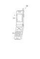
上述した電界駆動型装置としての液晶装置1は、例えば、図14に示すような、電子機器としての携帯電話機100に搭載して用いることができる。携帯電話機100は、表示部110及び操作ボタン120を有している。表示部110は、内部に組み込まれた液晶装置1によって、操作ボタン120で入力した内容や着信情報を始めとする様々な情報について、高品位な表示を行うことができる。
(Electronics)
The above-described
なお、液晶装置1は、上記携帯電話機100の他、モバイルコンピュータ、デジタルカメラ、デジタルビデオカメラ、車載機器、オーディオ機器などの各種電子機器に用いることができる。
The
上記実施形態に対しては、様々な変形を加えることができる。変形例としては、例えば以下のようなものが考えられる。 Various modifications can be made to the above embodiment. As modifications, for example, the following can be considered.
(変形例1)
遮光性部材として、信号線14、遮光層13の他に、例えば走査線12を用いてもよい。図10は、遮光性部材として走査線12を用いた場合の画素領域5の拡大平面図である。走査線12は、Y方向に隣り合う画素4の境界を含む領域に、X方向に沿って帯状に形成されている。走査線12のY方向の幅は、第2電極26の接続部26AのY方向の幅より大きくなっている。また、接続部26Aのエッジ部26aは、平面視で走査線12と重なる位置に配置されている。したがって、スリット27のうちエッジ部26aの近傍領域は、平面視で走査線12によって遮光され、この部位における光学特性の低下を抑制することが可能となる。
(Modification 1)
As the light shielding member, in addition to the
また、走査線12の各部は、平面視で、第1電極16及び第2電極26の少なくとも一方と重なっている。このような構成によれば、走査線12からの電界が第1電極16、第2電極26のいずれかによって遮蔽されるため、走査線12の近傍における光学特性の低下を抑制することができる。
Each part of the
(変形例2)
遮光性部材として、対向電極配線を用いてもよい。図11は、遮光性部材として対向電極配線17を用いた場合の画素領域5の拡大平面図である。対向電極配線17は、Y方向に隣り合う画素4の境界を含む領域に、X方向に沿って帯状に形成されている。対向電極配線17は、例えば走査線12と同一の層に、同一の材料で形成することができる。対向電極配線17は、図示しないコンタクトホールを介して第2電極26と電気的に接続されており、第2電極26を所定の電位に保つために用いられる。
(Modification 2)
A counter electrode wiring may be used as the light shielding member. FIG. 11 is an enlarged plan view of the
対向電極配線17のY方向の幅は、第2電極26の接続部26AのY方向の幅より大きくなっている。また、接続部26Aのエッジ部26aは、平面視で対向電極配線17と重なる位置に配置されている。したがって、スリット27のうちエッジ部26aの近傍領域は、平面視で対向電極配線17によって遮光され、この部位における光学特性の低下を抑制することが可能となる。
The width in the Y direction of the
また、対向電極配線17の各部は、平面視で、第1電極16及び第2電極26の少なくとも一方と重なっている。このような構成によれば、対向電極配線17からの電界が第1電極16、第2電極26のいずれかによって遮蔽されるため、対向電極配線17の近傍における光学特性の低下を抑制することができる。
Each part of the
(変形例3)
遮光性部材としては、信号線14、遮光層13、走査線12、対向電極配線17に代えて、これらのうちの1つと同一の層に形成された同一の部材を含んで構成することもできる。
(Modification 3)
As the light shielding member, instead of the
(変形例4)
上記各実施形態は、第1電極16を画素電極とし、これより上層に位置する第2電極26を共通電極とするものであるが、これに代えて、第1電極16を共通電極とし、これより上層に、画素電極としての第2電極26を配置してもよい。
(Modification 4)
In each of the above embodiments, the
図12は、本変形例に係る液晶装置1の画素領域5の拡大平面図である。図12は、第2の実施形態の液晶装置1に本変形例を適用した例である。第2電極26は、画素4ごとに矩形の外形を有して形成されている。第2電極26には、スリット27が設けられている。第2電極26は、コンタクトホール25を介して半導体層21のドレイン領域に電気的に接続されている。第2電極26の下層に形成された第1電極16は、複数の画素4にわたって一繋がりに形成された共通電極となっている。こうした構成によっても、第1電極16と第2電極26との間に駆動電圧を印加することで、液晶50の層に横電界を発生させることができる。
FIG. 12 is an enlarged plan view of the
本変形例の構成においても、第2電極26の接続部26Aのエッジ部26aは、平面視で遮光層13と重なる位置に配置されている。したがって、スリット27のうちエッジ部26aの近傍領域は、平面視で遮光層13によって遮光され、この部位における光学特性の低下を抑制することが可能となる。
Also in the configuration of this modification, the
また、遮光層13の各部は、平面視で、第1電極16及び第2電極26の少なくとも一方と重なっている。このような構成によれば、遮光層13からの電界が第1電極16、第2電極26のいずれかによって遮蔽されるため、遮光層13の近傍における光学特性の低下を抑制することができる。特に、本変形例では、第1電極16は画素4ごとに分断されておらず、またスリットもなく、画素領域5の略全面にわたって形成されているため、遮光層13をはじめ、走査線12、信号線14等の各種配線を覆うように形成でき、これらの配線からの電界を広く遮蔽することができる。
Each part of the
(変形例5)
上記実施形態では、電界駆動型装置の一例として液晶装置1について説明したが、これに限定する趣旨ではない。電界駆動型装置は、第1電極16と第2電極26との間の電位差(駆動電圧)に起因して生じる電界によって物質を駆動する構成であればよく、液晶装置に限定されない。
(Modification 5)
In the above embodiment, the
1…電界駆動型装置としての液晶装置、4…画素、5…画素領域、10…素子基板、11,31…ガラス基板、12…走査線、13…遮光層、14…信号線、15…中継電極、16…第1電極、17…対向電極配線、18,38…配向膜、20…TFT素子、21…半導体層、21a…チャネル領域、23,24,25…コンタクトホール、26…第2電極、26A…接続部、26B…帯状部、26a…エッジ部、27…スリット、30…対向基板、32…カラーフィルタ、41,43,44,45…層間絶縁膜、42…ゲート絶縁膜、46…保護層、50…液晶、50a…液晶分子、51…ドライバIC、52…シール材、100…携帯電話機。
DESCRIPTION OF
Claims (7)
前記複数のスリットは、前記延在方向と交差した所定方向に配列する第1のスリットと、前記所定方向と直交した方向であって配列した前記第1のスリットの短辺の側で該第1のスリットに隣り合って配置される第2のスリットと、を有し、
前記遮光性部材は、前記第1のスリットの前記第2のスリット側のエッジ部と、前記第2のスリットの前記第1のスリット側のエッジ部と、の間の前記所定方向に直交した方向における幅よりも大きい幅で形成され、
前記遮光性部材は、前記第1のスリットの前記第2のスリット側のエッジ部と前記第2のスリットの前記第1のスリット側のエッジ部との間の領域を覆って平面視で重ねて配置されているとともに、前記第1電極の前記第1のスリットと前記第2のスリットとが隣り合う側の端部と平面視で重ねて配置されていることを特徴とする電界駆動型装置。 A liquid crystal is sandwiched between a pair of substrates, a thin film transistor element formed for each pixel on the liquid crystal side of one of the pair of substrates, and a signal line electrically connected to the thin film transistor element or the A light-shielding member including the same member as the signal line formed in the same layer as the signal line , a first electrode, an insulating layer formed on the liquid crystal side of the first electrode, and the insulating layer A second electrode formed on the liquid crystal side, wherein the second electrode overlaps with the first electrode in plan view and has a plurality of openings having an extending direction. An electric field driving type device in which a slit is formed, and the liquid crystal is driven by an electric field generated due to a potential difference between the first electrode and the second electrode,
The plurality of slits includes a first slit arranged in a predetermined direction intersecting the extending direction, and a first side on a short side of the first slit arranged in a direction orthogonal to the predetermined direction. A second slit disposed adjacent to the slit of
The light shielding member has a direction orthogonal to the predetermined direction between an edge portion of the first slit on the second slit side and an edge portion of the second slit on the first slit side. Formed with a width greater than the width at
The light-shielding member covers the region between the second slit-side edge portion of the first slit and the first slit-side edge portion of the second slit, and is overlapped in a plan view. An electric field drive type device characterized in that the first slit and the second slit of the first electrode are arranged so as to overlap with an end portion on an adjacent side in plan view.
前記遮光性部材は、複数の前記第1のスリットの前記第2のスリット側のエッジ部と前記第2のスリットの前記第1のスリット側のエッジ部との間の領域を覆って、前記所定方向に帯状に延在して形成されていることを特徴とする電界駆動型装置。 It is an electric field drive type device according to claim 1,
The light-shielding member covers an area between the second slit side edge portion of the plurality of first slits and the first slit side edge portion of the second slit, and An electric field drive type device characterized by being formed to extend in a band shape in a direction.
前記遮光性部材の各部は、平面視で、前記第1電極及び前記第2電極の少なくとも一方と重なっていることを特徴とする電界駆動型装置。 The electric field drive type device according to claim 1 or 2,
Each part of the light shielding member overlaps at least one of the first electrode and the second electrode in a plan view.
前記複数のスリットは、前記延在方向と交差した所定方向に配列する第1のスリットと、前記所定方向と直交した方向であって配列した前記第1のスリットの短辺の側で該第1のスリットに隣り合って配置される第2のスリットと、を有し、
前記遮光性部材は、前記第1のスリットの前記第2のスリット側のエッジ部と、前記第2のスリットの前記第1のスリット側のエッジ部と、の間の前記所定方向に直交した方向における幅よりも大きい幅で形成され、
前記遮光性部材は、前記第1のスリットの前記第2のスリット側のエッジ部と前記第2のスリットの前記第1のスリット側のエッジ部との間の領域を覆って平面視で重ねて配置されているとともに、前記第1電極の前記第1のスリットと前記第2のスリットとが隣り合う側の端部と平面視で重ねて配置されており、
前記遮光性部材は、前記第2電極と電気的に接続された対向電極配線又は前記対向電極配線と同一の層に形成された前記対向電極配線と同一の部材を含んで構成されることを特徴とする電界駆動型装置。 A liquid crystal is sandwiched between a pair of substrates, a light shielding member, a first electrode, and an insulating layer formed on the liquid crystal side of the first electrode on the liquid crystal side of one of the pair of substrates. And a second electrode formed on the liquid crystal side of the insulating layer, and the second electrode has an extending direction at least partially overlapping the first electrode in a plan view. A plurality of slits opened in an outer shape are formed, and the liquid crystal is driven by an electric field generated due to a potential difference between the first electrode and the second electrode,
The plurality of slits includes a first slit arranged in a predetermined direction intersecting the extending direction, and a first side on a short side of the first slit arranged in a direction orthogonal to the predetermined direction. A second slit disposed adjacent to the slit of
The light shielding member has a direction orthogonal to the predetermined direction between an edge portion of the first slit on the second slit side and an edge portion of the second slit on the first slit side. Formed with a width greater than the width at
The light-shielding member covers the region between the second slit-side edge portion of the first slit and the first slit-side edge portion of the second slit, and is overlapped in a plan view. And the first slit and the second slit of the first electrode are arranged so as to overlap with an end portion on the adjacent side in a plan view,
The light-shielding member includes a counter electrode wiring electrically connected to the second electrode or the same member as the counter electrode wiring formed in the same layer as the counter electrode wiring. Electric field drive type device.
前記複数のスリットは、前記延在方向と交差した所定方向に配列する第1のスリットと、前記所定方向と直交した方向であって配列した前記第1のスリットの短辺の側で該第1のスリットに隣り合って配置される第2のスリットと、を有し、The plurality of slits includes a first slit arranged in a predetermined direction intersecting the extending direction, and a first side on a short side of the first slit arranged in a direction orthogonal to the predetermined direction. A second slit disposed adjacent to the slit of
前記遮光性部材は、前記第1のスリットの前記第2のスリット側のエッジ部と、前記第2のスリットの前記第1のスリット側のエッジ部と、の間の前記所定方向に直交した方向における幅よりも大きい幅で形成され、The light shielding member has a direction orthogonal to the predetermined direction between an edge portion of the first slit on the second slit side and an edge portion of the second slit on the first slit side. Formed with a width greater than the width at
前記遮光性部材は、前記第1のスリットの前記第2のスリット側のエッジ部と前記第2のスリットの前記第1のスリット側のエッジ部との間の領域を覆って平面視で重ねて配置されているとともに、前記第1電極の前記第1のスリットと前記第2のスリットとが隣り合う側の端部と平面視で重ねて配置されていることを特徴とする電界駆動型装置。The light-shielding member covers the region between the second slit-side edge portion of the first slit and the first slit-side edge portion of the second slit, and is overlapped in a plan view. An electric field drive type device characterized in that the first slit and the second slit of the first electrode are arranged so as to overlap with an end portion on an adjacent side in plan view.
Priority Applications (1)
| Application Number | Priority Date | Filing Date | Title |
|---|---|---|---|
| JP2007319275A JP5088687B2 (en) | 2007-12-11 | 2007-12-11 | Electric field driving apparatus and electronic apparatus |
Applications Claiming Priority (1)
| Application Number | Priority Date | Filing Date | Title |
|---|---|---|---|
| JP2007319275A JP5088687B2 (en) | 2007-12-11 | 2007-12-11 | Electric field driving apparatus and electronic apparatus |
Publications (3)
| Publication Number | Publication Date |
|---|---|
| JP2009145367A JP2009145367A (en) | 2009-07-02 |
| JP2009145367A5 JP2009145367A5 (en) | 2010-12-24 |
| JP5088687B2 true JP5088687B2 (en) | 2012-12-05 |
Family
ID=40916074
Family Applications (1)
| Application Number | Title | Priority Date | Filing Date |
|---|---|---|---|
| JP2007319275A Expired - Fee Related JP5088687B2 (en) | 2007-12-11 | 2007-12-11 | Electric field driving apparatus and electronic apparatus |
Country Status (1)
| Country | Link |
|---|---|
| JP (1) | JP5088687B2 (en) |
Families Citing this family (7)
| Publication number | Priority date | Publication date | Assignee | Title |
|---|---|---|---|---|
| US9480202B2 (en) | 2013-12-20 | 2016-11-01 | Harvest Croo, Llc | Automated selective harvesting of crops |
| US9913428B2 (en) | 2013-12-20 | 2018-03-13 | Harvest Croo, Llc | Individual plant location positioning |
| US11483975B2 (en) | 2013-12-20 | 2022-11-01 | Harvest Croo, Llc | Harvester pick deck suspension |
| US9897429B2 (en) | 2013-12-20 | 2018-02-20 | Harvest Croo, Llc | Harvester suspension |
| US9888631B2 (en) | 2013-12-20 | 2018-02-13 | Harvest Croo, Llc | Foliage holding |
| US9888630B2 (en) | 2013-12-20 | 2018-02-13 | Harvest Croo, Llc | Robot positioning with station-keeping |
| US9554513B2 (en) | 2013-12-20 | 2017-01-31 | Harvest Croo, Llc | Automated selective harvesting of crops with continuous offload |
Family Cites Families (1)
| Publication number | Priority date | Publication date | Assignee | Title |
|---|---|---|---|---|
| JP2009109616A (en) * | 2007-10-29 | 2009-05-21 | Sony Corp | Liquid crystal display |
-
2007
- 2007-12-11 JP JP2007319275A patent/JP5088687B2/en not_active Expired - Fee Related
Also Published As
| Publication number | Publication date |
|---|---|
| JP2009145367A (en) | 2009-07-02 |
Similar Documents
| Publication | Publication Date | Title |
|---|---|---|
| US11852923B2 (en) | Liquid crystal display device | |
| US8743330B2 (en) | Liquid crystal display device | |
| JP5167781B2 (en) | Electric field drive type device, liquid crystal device and electronic device | |
| JP5553531B2 (en) | Liquid crystal display | |
| JP5100968B2 (en) | Thin film transistor display panel and liquid crystal display device including the same | |
| EP1970752B1 (en) | Electric field driving device | |
| US8908114B2 (en) | Liquid crystal display device | |
| JP5192941B2 (en) | Liquid crystal display | |
| JP5088687B2 (en) | Electric field driving apparatus and electronic apparatus | |
| JP2010134294A5 (en) | ||
| JP5522243B2 (en) | Electric field driving apparatus and electronic apparatus | |
| JP4952166B2 (en) | Liquid crystal device | |
| JP2009145366A (en) | Field driven type device and electronic apparatus | |
| JP5736895B2 (en) | Horizontal electric field type liquid crystal display device | |
| JP2018138961A (en) | Liquid crystal display panel and liquid crystal display | |
| JP4065645B2 (en) | Active matrix liquid crystal display device | |
| JP4466708B2 (en) | Liquid crystal device | |
| JP2010175790A (en) | Liquid crystal display device | |
| US11143922B2 (en) | Display device | |
| JP2009251417A (en) | Liquid crystal display device | |
| JP5213616B2 (en) | Liquid crystal device, method for manufacturing liquid crystal device, and electronic apparatus | |
| JP2019040120A (en) | Liquid crystal display device | |
| JP5595678B2 (en) | Liquid crystal display | |
| JP2008233424A (en) | Liquid crystal display and manufacturing method therefor | |
| JP2019113656A (en) | Liquid crystal panel |
Legal Events
| Date | Code | Title | Description |
|---|---|---|---|
| A521 | Written amendment |
Free format text: JAPANESE INTERMEDIATE CODE: A523 Effective date: 20101109 |
|
| A621 | Written request for application examination |
Free format text: JAPANESE INTERMEDIATE CODE: A621 Effective date: 20101109 |
|
| A977 | Report on retrieval |
Free format text: JAPANESE INTERMEDIATE CODE: A971007 Effective date: 20120704 |
|
| A131 | Notification of reasons for refusal |
Free format text: JAPANESE INTERMEDIATE CODE: A131 Effective date: 20120710 |
|
| A521 | Written amendment |
Free format text: JAPANESE INTERMEDIATE CODE: A523 Effective date: 20120727 |
|
| TRDD | Decision of grant or rejection written | ||
| A01 | Written decision to grant a patent or to grant a registration (utility model) |
Free format text: JAPANESE INTERMEDIATE CODE: A01 Effective date: 20120820 |
|
| A01 | Written decision to grant a patent or to grant a registration (utility model) |
Free format text: JAPANESE INTERMEDIATE CODE: A01 |
|
| FPAY | Renewal fee payment (event date is renewal date of database) |
Free format text: PAYMENT UNTIL: 20150921 Year of fee payment: 3 |
|
| R150 | Certificate of patent or registration of utility model |
Ref document number: 5088687 Country of ref document: JP Free format text: JAPANESE INTERMEDIATE CODE: R150 Free format text: JAPANESE INTERMEDIATE CODE: R150 |
|
| A61 | First payment of annual fees (during grant procedure) |
Free format text: JAPANESE INTERMEDIATE CODE: A61 Effective date: 20120902 |
|
| S531 | Written request for registration of change of domicile |
Free format text: JAPANESE INTERMEDIATE CODE: R313531 |
|
| R350 | Written notification of registration of transfer |
Free format text: JAPANESE INTERMEDIATE CODE: R350 |
|
| LAPS | Cancellation because of no payment of annual fees |