JP5141780B2 - Rotation angle sensor - Google Patents
Rotation angle sensor Download PDFInfo
- Publication number
- JP5141780B2 JP5141780B2 JP2011003552A JP2011003552A JP5141780B2 JP 5141780 B2 JP5141780 B2 JP 5141780B2 JP 2011003552 A JP2011003552 A JP 2011003552A JP 2011003552 A JP2011003552 A JP 2011003552A JP 5141780 B2 JP5141780 B2 JP 5141780B2
- Authority
- JP
- Japan
- Prior art keywords
- magnet
- magnetic field
- magnetic sensor
- magnetic
- rotation axis
- Prior art date
- Legal status (The legal status is an assumption and is not a legal conclusion. Google has not performed a legal analysis and makes no representation as to the accuracy of the status listed.)
- Active
Links
Images

Classifications
-
- G—PHYSICS
- G01—MEASURING; TESTING
- G01R—MEASURING ELECTRIC VARIABLES; MEASURING MAGNETIC VARIABLES
- G01R33/00—Arrangements or instruments for measuring magnetic variables
- G01R33/02—Measuring direction or magnitude of magnetic fields or magnetic flux
- G01R33/06—Measuring direction or magnitude of magnetic fields or magnetic flux using galvano-magnetic devices
- G01R33/09—Magnetoresistive devices
- G01R33/091—Constructional adaptation of the sensor to specific applications
-
- G—PHYSICS
- G01—MEASURING; TESTING
- G01D—MEASURING NOT SPECIALLY ADAPTED FOR A SPECIFIC VARIABLE; ARRANGEMENTS FOR MEASURING TWO OR MORE VARIABLES NOT COVERED IN A SINGLE OTHER SUBCLASS; TARIFF METERING APPARATUS; MEASURING OR TESTING NOT OTHERWISE PROVIDED FOR
- G01D5/00—Mechanical means for transferring the output of a sensing member; Means for converting the output of a sensing member to another variable where the form or nature of the sensing member does not constrain the means for converting; Transducers not specially adapted for a specific variable
- G01D5/12—Mechanical means for transferring the output of a sensing member; Means for converting the output of a sensing member to another variable where the form or nature of the sensing member does not constrain the means for converting; Transducers not specially adapted for a specific variable using electric or magnetic means
- G01D5/14—Mechanical means for transferring the output of a sensing member; Means for converting the output of a sensing member to another variable where the form or nature of the sensing member does not constrain the means for converting; Transducers not specially adapted for a specific variable using electric or magnetic means influencing the magnitude of a current or voltage
- G01D5/142—Mechanical means for transferring the output of a sensing member; Means for converting the output of a sensing member to another variable where the form or nature of the sensing member does not constrain the means for converting; Transducers not specially adapted for a specific variable using electric or magnetic means influencing the magnitude of a current or voltage using Hall-effect devices
- G01D5/145—Mechanical means for transferring the output of a sensing member; Means for converting the output of a sensing member to another variable where the form or nature of the sensing member does not constrain the means for converting; Transducers not specially adapted for a specific variable using electric or magnetic means influencing the magnitude of a current or voltage using Hall-effect devices influenced by the relative movement between the Hall device and magnetic fields
-
- G—PHYSICS
- G01—MEASURING; TESTING
- G01R—MEASURING ELECTRIC VARIABLES; MEASURING MAGNETIC VARIABLES
- G01R33/00—Arrangements or instruments for measuring magnetic variables
- G01R33/0011—Arrangements or instruments for measuring magnetic variables comprising means, e.g. flux concentrators, flux guides, for guiding or concentrating the magnetic flux, e.g. to the magnetic sensor
Landscapes
- Physics & Mathematics (AREA)
- General Physics & Mathematics (AREA)
- Condensed Matter Physics & Semiconductors (AREA)
- Transmission And Conversion Of Sensor Element Output (AREA)
- Measuring Magnetic Variables (AREA)
Abstract
Description
本発明は、回転する磁石と、磁石による磁界を検出する磁気センサとを備え、磁石の回転角度を検出する回転角度センサに関する。 The present invention relates to a rotation angle sensor that includes a rotating magnet and a magnetic sensor that detects a magnetic field generated by the magnet, and detects a rotation angle of the magnet.
近年、自動車のステアリングの回転位置の検出等の種々の用途で、対象物の回転位置を検出するために、磁気式の回転角度センサが広く利用されている。磁気式の回転角度センサとしては、例えば、特許文献1,2に記載されているように、回転する磁石と、磁石による磁界を検出する磁気センサとを備え、磁気センサの検出出力に基づいて磁石の回転角度を検出するものが知られている。
In recent years, magnetic rotation angle sensors have been widely used to detect the rotation position of an object in various applications such as detection of the rotation position of a steering wheel of an automobile. As a magnetic rotation angle sensor, for example, as described in
磁石と磁気センサとを備えた回転角度センサでは、例えば、磁石は、回転軸に垂直な端面を有すると共に回転軸に垂直な方向の磁化を有し、磁気センサは、磁石の端面に対して所定の間隔を開けて対向するように配置される。このような構成の回転角度センサに求められる性能としては、磁石によって発生されて磁気センサに印加される磁界の強度が大きいことと、磁石の実際の回転角度と磁気センサの検出出力に基づいて検出された磁石の回転角度(以下、検出角度と言う。)との差(以下、角度誤差と言う。)が小さいことが挙げられる。 In a rotation angle sensor including a magnet and a magnetic sensor, for example, the magnet has an end surface perpendicular to the rotation axis and magnetization in a direction perpendicular to the rotation axis, and the magnetic sensor has a predetermined value relative to the end surface of the magnet. Are arranged so as to face each other with a gap therebetween. The performance required for the rotation angle sensor having such a configuration is that the intensity of the magnetic field generated by the magnet and applied to the magnetic sensor is large, and the detection is based on the actual rotation angle of the magnet and the detection output of the magnetic sensor. The difference (hereinafter referred to as an angle error) with respect to the rotation angle of the magnet (hereinafter referred to as a detection angle) is small.
磁気センサには、磁石が発生する磁界の他に、モーターからの漏れ磁界や地磁気等の他の磁界が印加される場合がある。磁石によって発生されて磁気センサに印加される磁界の強度が大きいことは、磁気センサに印加される磁界のうち、磁石が発生する磁界以外の磁界の影響を相対的に小さくするために必要である。磁石によって発生されて磁気センサに印加される磁界の強度を大きくすることは、例えば、残留磁束密度の大きな磁性材料によって磁石を形成したり、磁石を大型にしたりすることによって実現される。 In addition to the magnetic field generated by the magnet, other magnetic fields such as a leakage magnetic field from the motor and geomagnetism may be applied to the magnetic sensor. The strength of the magnetic field generated by the magnet and applied to the magnetic sensor is necessary to relatively reduce the influence of the magnetic field applied to the magnetic sensor other than the magnetic field generated by the magnet. . Increasing the strength of the magnetic field generated by the magnet and applied to the magnetic sensor is realized, for example, by forming the magnet with a magnetic material having a large residual magnetic flux density or increasing the size of the magnet.
一方、角度誤差を発生させる原因の一つに、磁石と磁気センサの位置関係のずれがある。磁石と磁気センサの位置関係は、回転角度センサの作製時点や、回転角度センサの使用時において、所望の位置関係からわずかにずれる場合がある。ここで、磁石の端面に平行な仮想の平面上において回転軸が交わる位置(以下、中心位置と言う。)では、磁石による磁界の方向が磁石の磁化の方向と平行であるものとする。そして、仮想の平面上において、回転軸が磁気センサの中心を通過するような磁気センサの位置を、磁気センサの所望の位置とする。上記の仮想の平面上において、中心位置から離れた位置では、磁石による磁界の方向は、中心位置における磁石による磁界の方向とは異なる場合がある。そのため、仮想の平面上において、磁気センサの位置が所望の位置からずれた場合には、磁気センサによって検出される磁界の方向が、所望の位置に配置されたときに磁気センサによって検出される磁界の方向とは異なる場合が起こり得る。このようにして、磁石と磁気センサの位置関係のずれに起因して角度誤差が発生し得る。回転角度センサには、磁石と磁気センサの位置関係のずれが生じた場合であっても、角度誤差が小さいことが求められる。 On the other hand, one of the causes for causing an angle error is a shift in the positional relationship between the magnet and the magnetic sensor. The positional relationship between the magnet and the magnetic sensor may slightly deviate from the desired positional relationship when the rotational angle sensor is manufactured or when the rotational angle sensor is used. Here, it is assumed that the direction of the magnetic field by the magnet is parallel to the direction of magnetization of the magnet at a position where the rotation axes intersect on a virtual plane parallel to the end face of the magnet (hereinafter referred to as the center position). Then, on the virtual plane, the position of the magnetic sensor such that the rotation axis passes through the center of the magnetic sensor is set as a desired position of the magnetic sensor. On the virtual plane, at a position away from the center position, the direction of the magnetic field by the magnet may be different from the direction of the magnetic field by the magnet at the center position. Therefore, when the position of the magnetic sensor deviates from a desired position on the virtual plane, the direction of the magnetic field detected by the magnetic sensor is the magnetic field detected by the magnetic sensor when placed at the desired position. There may be cases where the direction is different. In this way, an angle error can occur due to a shift in the positional relationship between the magnet and the magnetic sensor. The rotation angle sensor is required to have a small angle error even when the positional relationship between the magnet and the magnetic sensor is shifted.
特許文献1には、円板磁石と磁電変換素子とを備えた回転角度センサにおいて、磁電変換素子を、円板磁石の回転軸ずれによる角度誤差が小さくなる位置に配置することによって、角度誤差を抑える技術が記載されている。
In
特許文献2には、磁石の形状と磁気検出部の配置を工夫することにより、角度誤差を低減する技術が記載されている。この技術において、磁石は、回転中心軸の近傍部と、近傍部の外側の第1外周部と、第1外周部の外側の第2外周部とを有している。近傍部の回転中心軸に平行な方向の厚さは、第1外周部および第2外周部の回転中心軸に平行な方向の厚さよりも厚い。
前述のように、回転する磁石と磁気センサとを備えた回転角度センサでは、磁石によって発生されて磁気センサに印加される磁界の強度が大きいことと、磁石と磁気センサの位置関係のずれに起因した角度誤差が小さいことが求められる。これらの要求を満たすために、磁石が発生する磁界の強度を大きくすると共に、磁石と磁気センサの位置関係のずれに起因した角度誤差が小さくなるような位置に磁気センサを配置することが考えられる。 As described above, in the rotation angle sensor including the rotating magnet and the magnetic sensor, the strength of the magnetic field generated by the magnet and applied to the magnetic sensor is large, and the positional relationship between the magnet and the magnetic sensor is shifted. The required angle error is required to be small. In order to satisfy these requirements, it is conceivable to increase the intensity of the magnetic field generated by the magnet and to arrange the magnetic sensor at a position where the angular error due to the positional relationship between the magnet and the magnetic sensor is reduced. .
本願の発明者らは、シミュレーションによって、円柱形状の磁石の端面の近傍に、その領域内の磁界の方向が所望の位置における磁界の方向と実質的に同じ方向となる領域(以下、平行磁界領域と言う。)が存在することと、磁石の端面に平行な仮想の平面上における平行磁界領域の面積は、磁石の端面と仮想の平面との間の距離によって変化することを確認した。そこで、平行磁界領域の面積が最大になるような仮想の平面上に磁気センサを配置することで、磁石と磁気センサの位置関係のずれに起因した角度誤差を小さくすることができると考えられる。 The inventors of the present application have shown by simulation that a region in which the direction of the magnetic field in the region is substantially the same as the direction of the magnetic field at a desired position (hereinafter referred to as a parallel magnetic field region). And the area of the parallel magnetic field region on the virtual plane parallel to the end surface of the magnet was confirmed to change depending on the distance between the end surface of the magnet and the virtual plane. Therefore, it is considered that the angular error due to the positional relationship between the magnet and the magnetic sensor can be reduced by arranging the magnetic sensor on a virtual plane that maximizes the area of the parallel magnetic field region.
一方、円柱形状の磁石が発生する磁界の強度を大きくするためには、磁石の厚み(回転軸方向の寸法)を大きくことが有効である。しかし、磁石の厚みを大きくする場合には、以下のような問題が生じることが分かった。すなわち、シミュレーションにより、磁石の厚みを大きくすると、平行磁界領域の面積が最大になるような仮想の平面と磁石の端面との間の距離が小さくなることが分かった。そのため、磁石の厚みを大きくし、且つ、平行磁界領域の面積が最大になるような仮想の平面上に磁気センサを配置すると、磁石の端面と磁気センサとの間の距離が小さくなりすぎて、磁気センサが磁石に接触して破損するおそれが生じる。 On the other hand, in order to increase the strength of the magnetic field generated by the cylindrical magnet, it is effective to increase the thickness of the magnet (dimension in the direction of the rotation axis). However, it has been found that the following problems occur when the thickness of the magnet is increased. That is, it has been found by simulation that when the magnet thickness is increased, the distance between the virtual plane that maximizes the area of the parallel magnetic field region and the end surface of the magnet is reduced. Therefore, when the magnetic sensor is arranged on an imaginary plane where the thickness of the magnet is increased and the area of the parallel magnetic field region is maximized, the distance between the end surface of the magnet and the magnetic sensor becomes too small, There is a risk that the magnetic sensor may be damaged by contact with the magnet.
このように、円柱形状の磁石を用いる場合には、磁石と磁気センサとの間の距離が小さくなりすぎることなく、磁石によって発生されて磁気センサに印加される磁界の強度を大きくし、且つ磁石と磁気センサの位置関係のずれに起因した角度誤差を低減することが困難であった。特許文献1,2に記載された技術では、この問題を解決することはできない。
Thus, when a cylindrical magnet is used, the strength of the magnetic field generated by the magnet and applied to the magnetic sensor is increased without the distance between the magnet and the magnetic sensor becoming too small, and the magnet It is difficult to reduce the angle error due to the positional difference between the magnetic sensor and the magnetic sensor. The techniques described in
本発明はかかる問題点に鑑みてなされたもので、その目的は、回転する磁石と、磁石による磁界を検出する磁気センサとを備え、磁石の回転角度を検出する回転角度センサであって、磁石と磁気センサとの間の距離が小さくなりすぎることなく、磁石によって発生されて磁気センサに印加される磁界の強度を大きくし、且つ磁石と磁気センサの位置関係のずれに起因した角度誤差を低減できるようにした回転角度センサを提供することにある。 The present invention has been made in view of such problems, and an object thereof is a rotation angle sensor that includes a rotating magnet and a magnetic sensor that detects a magnetic field by the magnet, and detects the rotation angle of the magnet. The magnetic field generated by the magnet and applied to the magnetic sensor is increased without reducing the distance between the magnetic sensor and the magnetic sensor, and the angular error due to the positional relationship between the magnet and the magnetic sensor is reduced. An object of the present invention is to provide a rotation angle sensor that can be used.
本発明の回転角度センサは、回転軸に垂直な端面を有すると共に回転軸に垂直な方向の磁化を有し、回転軸を中心として回転する磁石と、磁石の端面に対向して、磁石による磁界を検出する磁気センサとを備え、磁気センサの検出出力に基づいて磁石の回転角度を検出するものである。磁石は、端面を含む板状部と、板状部に対して端面とは反対側に配置されて板状部に連結されたリング状部とを有している。板状部は回転軸が通過する空洞を含まないが、リング状部は回転軸が通過する空洞を含んでいる。 The rotation angle sensor of the present invention has an end surface perpendicular to the rotation axis and magnetization in a direction perpendicular to the rotation axis, a magnet rotating around the rotation axis, and a magnetic field generated by the magnet facing the end surface of the magnet. And a rotation angle of the magnet based on the detection output of the magnetic sensor. The magnet has a plate-like portion including an end surface, and a ring-like portion that is arranged on the opposite side of the plate-like portion from the end surface and connected to the plate-like portion. The plate-like portion does not include a cavity through which the rotating shaft passes, but the ring-like portion includes a cavity through which the rotating shaft passes.
本発明の回転角度センサにおいて、磁石における回転軸を含む任意の断面の形状は、回転軸に対して線対称な形状であってもよい。この場合、板状部は円板形状を有し、回転軸に垂直なリング状部の任意の断面におけるリング状部の外周および内周はいずれも円形であってもよい。 In the rotation angle sensor of the present invention, the shape of an arbitrary cross section including the rotation axis of the magnet may be a line-symmetric shape with respect to the rotation axis. In this case, the plate-like portion has a disk shape, and the outer circumference and the inner circumference of the ring-like portion in any cross section of the ring-shaped portion perpendicular to the rotation axis may be circular.
また、本発明の回転角度センサにおいて、磁石の端面と磁気センサとの間の距離と等しい距離だけ端面から離れた位置にあり端面に平行な仮想の平面上で、回転軸が交わる第1の位置と、この第1の位置とは異なる第2の位置において、磁石による磁界の方向が互いに平行であってもよい。 In the rotation angle sensor of the present invention, the first position where the rotation axis intersects on a virtual plane parallel to the end surface at a position that is separated from the end surface by a distance equal to the distance between the end surface of the magnet and the magnetic sensor. And in the 2nd position different from this 1st position, the direction of the magnetic field by a magnet may mutually be parallel.
また、本発明の回転角度センサにおいて、磁気センサは、磁気抵抗効果素子を含んでいてもよい。 In the rotation angle sensor of the present invention, the magnetic sensor may include a magnetoresistive element.
本発明の回転角度センサでは、磁石は、磁気センサが対向する端面を含む板状部と、板状部に対して端面とは反対側に配置されて板状部に連結されたリング状部とを有し、板状部は回転軸が通過する空洞を含まないが、リング状部は回転軸が通過する空洞を含んでいる。本発明における磁石を用いることにより、例えば、磁石と磁気センサの位置関係のずれに起因した角度誤差が小さくなるような磁石の端面と磁気センサとの間の距離(以下、最適距離と言う。)が、ほぼ等しくなる条件で比較すると、円柱形状の磁石を用いる場合に比べて、磁石によって発生されて磁気センサに印加される磁界の強度を大きくすることができる。また、本発明における磁石を用いることにより、例えば、最適距離における上記磁界の強度がほぼ等しくなる条件で比較すると、円柱形状の磁石を用いる場合に比べて、最適距離を大きくすることができる。従って、本発明によれば、磁石と磁気センサとの間の距離が小さくなりすぎることなく、磁石によって発生されて磁気センサに印加される磁界の強度を大きくし、且つ磁石と磁気センサの位置関係のずれに起因した角度誤差を低減することが可能になるという効果を奏する。 In the rotation angle sensor of the present invention, the magnet includes a plate-like portion including an end face opposed to the magnetic sensor, and a ring-like portion disposed on the opposite side of the end face with respect to the plate-like portion and connected to the plate-like portion. The plate-shaped part does not include a cavity through which the rotating shaft passes, whereas the ring-shaped part includes a cavity through which the rotating shaft passes. By using the magnet according to the present invention, for example, the distance between the end surface of the magnet and the magnetic sensor (hereinafter referred to as the optimum distance) such that the angular error due to the positional relationship between the magnet and the magnetic sensor is reduced. However, when compared under substantially equal conditions, the strength of the magnetic field generated by the magnet and applied to the magnetic sensor can be increased as compared with the case of using a cylindrical magnet. Further, by using the magnet according to the present invention, for example, when the comparison is performed under the condition that the magnetic field strengths at the optimum distance are substantially equal, the optimum distance can be increased as compared with the case of using a cylindrical magnet. Therefore, according to the present invention, the distance between the magnet and the magnetic sensor does not become too small, the strength of the magnetic field generated by the magnet and applied to the magnetic sensor is increased, and the positional relationship between the magnet and the magnetic sensor. There is an effect that it is possible to reduce the angle error due to the deviation of the angle.
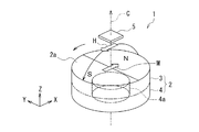
以下、本発明の実施の形態について図面を参照して詳細に説明する。始めに、図1ないし図7を参照して、本発明の一実施の形態に係る回転角度センサの概略の構成について説明する。図1は、本実施の形態に係る回転角度センサの概略の構成を示す斜視図である。図2は、図1に示した磁石を分解して示す斜視図である。図3は、本実施の形態に係る回転角度センサの概略の構成を示す側面図である。図4は、図3に示した回転角度センサにおける磁石と磁気センサを示す平面図である。図5は、図3に示した磁石の底面図である。図6は、図3に示した磁石の側面図である。図7は、本実施の形態における方向と角度の定義を示す説明図である。 Hereinafter, embodiments of the present invention will be described in detail with reference to the drawings. First, a schematic configuration of a rotation angle sensor according to an embodiment of the present invention will be described with reference to FIGS. FIG. 1 is a perspective view showing a schematic configuration of a rotation angle sensor according to the present embodiment. 2 is an exploded perspective view of the magnet shown in FIG. FIG. 3 is a side view showing a schematic configuration of the rotation angle sensor according to the present embodiment. FIG. 4 is a plan view showing a magnet and a magnetic sensor in the rotation angle sensor shown in FIG. FIG. 5 is a bottom view of the magnet shown in FIG. FIG. 6 is a side view of the magnet shown in FIG. FIG. 7 is an explanatory diagram showing definitions of directions and angles in the present embodiment.
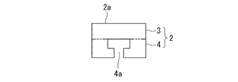
図1および図3に示したように、本実施の形態に係る回転角度センサ1は、磁石2と、基板8(図3参照)と、基板8に搭載された磁気センサ5とを備えている。磁石2は、回転軸Cを中心として回転する軸6の軸方向の一端部に、固定用治具7を介して固定されている。磁石2は、軸6の回転に連動して、回転軸Cを中心として回転する。
As shown in FIGS. 1 and 3, the
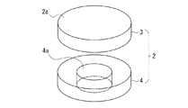
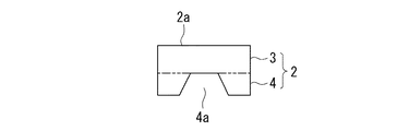
磁石2は、回転軸Cに垂直な端面2aを有すると共に回転軸Cに垂直な方向の磁化を有している。磁石2は、端面2aを含む板状部3と、板状部3に対して端面2aとは反対側に配置されて板状部3に連結されたリング状部4とを有している。板状部3は回転軸Cが通過する空洞を含まないが、リング状部4は回転軸Cが通過する空洞4aを含んでいる。
The
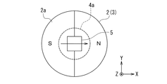
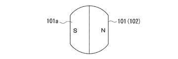
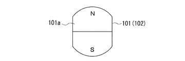
板状部3は、回転軸Cを含む仮想の平面を中心として対称に配置されたN極とS極を有している。磁石2の磁化の方向は、板状部3のS極からN極に向かう方向であって、S極とN極との境界に垂直な方向である。図1において、符号Mで示した矢印は、磁石2の磁化の方向を表している。板状部3とリング状部4は、磁石2の磁化の方向と同じ方向の磁化を有している。図4において、板状部3に描かれた矢印は、板状部3の磁化の方向を表している。図5において、リング状部4に描かれた矢印は、リング状部4の磁化の方向を表している。
The plate-
磁石2は、自身が有する磁化に基づいて磁界を発生する。図1において、符号Hで示した矢印は、端面2aの近傍であって回転軸C上の位置における磁石2による磁界の方向を表している。
The
基板8は、磁石2の端面2aに対向する面を有し、この面に磁気センサ5が固定されている。磁気センサ5は、磁石2の端面2aに対向して、磁石2による磁界を検出する。回転角度センサ1は、磁気センサ5の検出出力に基づいて磁石2の回転角度を検出する。
The
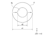
磁石2における回転軸Cを含む任意の断面の形状は、回転軸Cに対して線対称な形状である。図1ないし図7には、磁石2の形状の一例を示している。この例では、板状部3は円板形状を有し、回転軸Cに垂直なリング状部4の任意の断面におけるリング状部4の外周および内周はいずれも、回転軸Cを中心とした円形である。
The shape of an arbitrary cross section including the rotation axis C in the
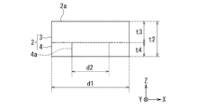
ここで、図5および図6に示したように、磁石2の直径を記号d1で表し、リング状部4の内径、すなわち空洞4aの直径を記号d2で表す。板状部3の直径とリング状部4の直径は、磁石2の直径d1と等しい。また、図6に示したように、磁石2、板状部3およびリング状部4の厚み(回転軸Cに平行な方向の寸法)を、それぞれ記号t2,t3,t4で表す。
Here, as shown in FIGS. 5 and 6, the diameter of the
次に、図7を参照して、本実施の形態における方向と角度の定義について説明する。まず、図1に示した回転軸Cに平行で、磁石2の端面2aから磁気センサ5に向かう方向をZ方向と定義する。次に、Z方向に垂直な仮想の平面上において、互いに直交する2つの方向をX方向とY方向と定義する。図7では、X方向を右側に向かう方向として表し、Y方向を上側に向かう方向として表している。また、X方向とは反対の方向を−X方向と定義し、Y方向とは反対の方向を−Y方向と定義する。
Next, the definition of the direction and angle in the present embodiment will be described with reference to FIG. First, a direction parallel to the rotation axis C shown in FIG. 1 and directed from the
また、磁石2の回転角度を表すために、空間における基準方向DRと、磁石2と共に回転する磁石基準方向DMとを定義する。基準方向DRは、例えばY方向とする。磁石基準方向DMは、例えば、磁石2の磁化の方向とは反対の方向とする。そして、磁石基準方向DMが基準方向DRに対してなす角度を、磁石2の回転角度θと定義する。磁石2および磁石基準方向DMは、図7において反時計回り方向に回転するものとする。角度θは、基準方向DRから反時計回り方向に見たときに正の値で表し、基準方向DRから時計回り方向に見たときに負の値で表す。
Further, in order to represent the rotation angle of the
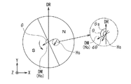
ここで、磁石2の端面2aと磁気センサ5との間の距離と等しい距離だけ端面2aから離れた位置にあり端面2aに平行な仮想の平面を考える。以下、この仮想の平面をセンサ配置面と呼ぶ。磁気センサ5は、実質的に、センサ配置面における、磁石2による磁界を検出する。センサ配置面上で、回転軸Cが交わる位置における、磁石2による磁界を記号H0で表す。磁界H0の方向は、磁石2の磁化の方向と平行であり、磁石基準方向DMと一致している。従って、磁界H0の方向が基準方向DRに対してなす角度は、角度θと一致する。
Here, let us consider a virtual plane parallel to the
また、センサ配置面上における、磁石2による磁界であって、磁気センサ5に印加される磁界を記号HSで表す。磁気センサ5は、この磁界HSを検出する。回転角度センサ1は、磁気センサ5の検出出力に基づいて、磁石2の回転角度θを検出する。実際には、回転角度センサ1は、磁気センサ5の検出出力に基づいて、回転角度θに対応する角度として、磁界HSの方向が基準方向DRに対してなす角度(以下、検出角度と言う。)θsを検出する。検出角度θsの正負の定義は、角度θと同様である。理想的には、検出角度θsは回転角度θと一致する。
Further, on the sensor arrangement surface, a magnetic field by the
回転軸Cが磁気センサ5の中心を通過するような磁気センサ5の位置を、磁気センサ5の所望の位置とする。磁気センサ5が所望の位置に配置されている場合には、磁界HSは磁界H0と等しくなるため、検出角度θsは回転角度θと等しくなる。しかし、センサ配置面上において、磁気センサ5が所望の位置からずれた位置に配置されている場合には、磁界HSの方向が磁界H0の方向とは異なる場合がある。図7は、この場合の例を示している。この場合、検出角度θsは回転角度θとは一致しない。検出角度θsと回転角度θとの差を角度誤差と呼び、記号dθで表す。図7に示した例では、角度誤差dθは、磁界HSの方向が磁界H0の方向に対してなす角度と等しい。角度誤差dθの正負の定義は、角度θと同様である。
A position of the
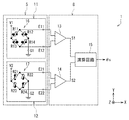
次に、図8を参照して、回転角度センサ1の回路構成について説明する。図8は、回転角度センサ1の回路構成を示す回路図である。磁気センサ5は、第1および第2の検出回路11,12を有している。基板8は、差分検出器13,14と演算回路15を有している。演算回路15は、例えば、マイクロコンピュータによって実現することができる。
Next, the circuit configuration of the
第1の検出回路11は、磁界HSの一方向の成分の強度を検出して、その強度を表す信号を出力する。第2の検出回路12は、磁界HSの他の一方向の成分の強度を検出して、その強度を表す信号を出力する。第1および第2の検出回路11,12は、少なくとも1つの磁気検出素子を含んでいる。
The
第1および第2の検出回路11,12は、それぞれ、少なくとも1つの磁気検出素子として、直列に接続された一対の磁気検出素子を含んでいてもよい。この場合、第1および第2の検出回路11,12は、それぞれ、直列に接続された第1の対の磁気検出素子と、直列に接続された第2の対の磁気検出素子とを含むホイートストンブリッジ回路を有していてもよい。以下、第1および第2の検出回路11,12が、それぞれ上記ホイートストンブリッジ回路を有している場合の例について説明する。
Each of the first and
第1の検出回路11は、ホイートストンブリッジ回路16を有している。ホイートストンブリッジ回路16は、電源ポートV1と、グランドポートG1と、2つの出力ポートE11,E12と、直列に接続された第1の対の磁気検出素子R11,R12と、直列に接続された第2の対の磁気検出素子R13,R14とを含んでいる。磁気検出素子R11,R13の各一端は、電源ポートV1に接続されている。磁気検出素子R11の他端は、磁気検出素子R12の一端と出力ポートE11に接続されている。磁気検出素子R13の他端は、磁気検出素子R14の一端と出力ポートE12に接続されている。磁気検出素子R12,R14の各他端は、グランドポートG1に接続されている。電源ポートV1には、所定の大きさの電源電圧が印加される。グランドポートG1はグランドに接続される。
The
第2の検出回路12は、ホイートストンブリッジ回路17を有している。ホイートストンブリッジ回路17は、電源ポートV2と、グランドポートG2と、2つの出力ポートE21,E22と、直列に接続された第1の対の磁気検出素子R21,R22と、直列に接続された第2の対の磁気検出素子R23,R24とを含んでいる。磁気検出素子R21,R23の各一端は、電源ポートV2に接続されている。磁気検出素子R21の他端は、磁気検出素子R22の一端と出力ポートE21に接続されている。磁気検出素子R23の他端は、磁気検出素子R24の一端と出力ポートE22に接続されている。磁気検出素子R22,R24の各他端は、グランドポートG2に接続されている。電源ポートV2には、所定の大きさの電源電圧が印加される。グランドポートG2はグランドに接続される。
The
本実施の形態では、ホイートストンブリッジ回路(以下、ブリッジ回路と記す。)16,17に含まれる全ての磁気検出素子として、MR素子、特にTMR素子を用いている。なお、TMR素子の代りにGMR素子を用いてもよい。TMR素子またはGMR素子は、磁化方向が固定された磁化固定層と、印加される磁界の方向に応じて磁化の方向が変化する自由層と、磁化固定層と自由層の間に配置された非磁性層とを有している。TMR素子では、非磁性層はトンネルバリア層である。GMR素子では、非磁性層は非磁性導電層である。TMR素子またはGMR素子では、自由層の磁化の方向が磁化固定層の磁化の方向に対してなす角度に応じて抵抗値が変化し、この角度が0°のときに抵抗値は最小値となり、角度が180°のときに抵抗値は最大値となる。以下の説明では、ブリッジ回路16,17に含まれる磁気検出素子をMR素子と記す。図8において、塗りつぶした矢印は、MR素子における磁化固定層の磁化の方向を表し、白抜きの矢印は、MR素子における自由層の磁化の方向を表している。
In the present embodiment, MR elements, particularly TMR elements, are used as all magnetic detection elements included in the Wheatstone bridge circuits (hereinafter referred to as bridge circuits) 16 and 17. A GMR element may be used in place of the TMR element. The TMR element or the GMR element includes a magnetization fixed layer whose magnetization direction is fixed, a free layer whose magnetization direction changes according to the direction of an applied magnetic field, and a non-magnetic layer disposed between the magnetization fixed layer and the free layer. And a magnetic layer. In the TMR element, the nonmagnetic layer is a tunnel barrier layer. In the GMR element, the nonmagnetic layer is a nonmagnetic conductive layer. In the TMR element or the GMR element, the resistance value changes according to the angle formed by the magnetization direction of the free layer with respect to the magnetization direction of the magnetization fixed layer, and when this angle is 0 °, the resistance value becomes the minimum value. When the angle is 180 °, the resistance value becomes the maximum value. In the following description, the magnetic detection elements included in the
第1の検出回路11では、MR素子R11,R14における磁化固定層の磁化の方向は−X方向であり、MR素子R12,R13における磁化固定層の磁化の方向はX方向である。この場合、磁界HSの−X方向の成分の強度に応じて、出力ポートE11,E12の電位差が変化する。従って、第1の検出回路11は、磁界HSの−X方向の成分の強度を検出して、その強度を表す信号を出力する。具体的には、出力ポートE11,E12の電位差が、第1の検出回路11の出力信号である。図7に示した角度θsが0°のときと180°のときは、磁界HSの−X方向の成分の強度は0である。角度θsが0°よりも大きく180°よりも小さいときは、磁界HSの−X方向の成分の強度は正の値である。角度θsが180°よりも大きく360°よりも小さいときは、磁界HSの−X方向の成分の強度は負の値である。
In the
第2の検出回路12では、MR素子R21,R24における磁化固定層の磁化の方向はY方向であり、MR素子R22,R23における磁化固定層の磁化の方向は−Y方向である。この場合、磁界HSのY方向の成分の強度に応じて、出力ポートE21,E22の電位差が変化する。従って、第2の検出回路12は、磁界HSのY方向の成分の強度を検出して、その強度を表す信号を出力する。具体的には、出力ポートE21,E22の電位差が、第2の検出回路12の出力信号である。図7に示した角度θsが90°のときと270°のときは、磁界HSのY方向の成分の強度は0である。角度θsが0°以上90°未満のとき、および270°より大きく360°以下のときは、磁界HSのY方向の成分の強度は正の値である。角度θsが90°よりも大きく270°よりも小さいときは、磁界HSのY方向の成分の強度は負の値である。
In the
差分検出器13は、出力ポートE11,E12の電位差に対応する信号を第1の信号S1として演算回路15に出力する。差分検出器14は、出力ポートE21,E22の電位差に対応する信号を第2の信号S2として演算回路15に出力する。第1の信号S1と第2の信号S2は、互いに等しい信号周期Tで周期的に変化する。本実施の形態では、第2の信号S2の位相は、第1の信号S1の位相に対して、信号周期Tの1/4の奇数倍だけ異なっていることが好ましい。ただし、磁気検出素子の作製の精度等の観点から、第1の信号S1と第2の信号S2の位相差は、信号周期Tの1/4の奇数倍から、わずかにずれていてもよい。以下の説明では、第1の信号S1と第2の信号S2の位相の関係が上記の好ましい関係になっているものとする。
The
図8に示した例では、第2の検出回路12におけるMR素子の磁化固定層の磁化方向は、第1の検出回路11におけるMR素子の磁化固定層の磁化方向に直交している。理想的には、第1の信号S1の波形はサイン(Sine)波形になり、第2の信号S2の波形はコサイン(Cosine)波形になる。この場合、第2の信号S2の位相は、第1の信号S1の位相に対して、信号周期Tの1/4すなわちπ/2(90°)だけ異なっている。演算回路15は、第1の信号S1および第2の信号S2に基づいて、検出角度θsを算出する。具体的には、例えば、演算回路15は、下記の式(1)によって、θsを算出する。なお、“atan”は、アークタンジェントを表す。
In the example illustrated in FIG. 8, the magnetization direction of the magnetization fixed layer of the MR element in the
θs=atan(S1/S2) …(1) θs = atan (S1 / S2) (1)
式(1)におけるatan(S1/S2)は、θsを求めるアークタンジェント計算を表している。なお、360°の範囲内で、式(1)におけるθsの解には、180°異なる2つの値がある。しかし、S1とS2の正負の組み合わせにより、θsの真の値が、式(1)におけるθsの2つの解のいずれであるかを判別することができる。すなわち、S1が正の値のときは、θsは0°よりも大きく180°よりも小さい。S1が負の値のときは、θsは180°よりも大きく360°よりも小さい。S2が正の値のときは、θsは、0°以上90°未満、および270°より大きく360°以下の範囲内である。S2が負の値のときは、θsは90°よりも大きく270°よりも小さい。演算回路15は、式(1)と、上記のS1とS2の正負の組み合わせの判定により、360°の範囲内でθsを求める。
Atan (S1 / S2) in equation (1) represents arctangent calculation for obtaining θs. Note that within the range of 360 °, the solution of θs in Equation (1) has two values that differ by 180 °. However, it is possible to determine which of the two solutions of θs in Equation (1) is the true value of θs by the positive / negative combination of S1 and S2. That is, when S1 is a positive value, θs is larger than 0 ° and smaller than 180 °. When S1 is a negative value, θs is larger than 180 ° and smaller than 360 °. When S2 is a positive value, θs is in the range of 0 ° to less than 90 ° and greater than 270 ° to 360 °. When S2 is a negative value, θs is greater than 90 ° and smaller than 270 °. The
なお、第2の信号S2の位相が、第1の信号S1の位相に対して、信号周期Tの1/4だけ異なる場合に限らず、第2の信号S2の位相が、第1の信号S1の位相に対して、信号周期Tの1/4の奇数倍だけ異なっていれば、θsを求めることができる。 Note that the phase of the second signal S2 is not limited to the case where the phase of the first signal S1 is different from the phase of the first signal S1 by ¼ of the signal period T, and the phase of the second signal S2 is the first signal S1. Θs can be obtained if the phase differs by an odd multiple of 1/4 of the signal period T.
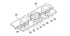
次に、図9を参照して、MR素子の構成の一例について説明する。図9は、図8に示した磁気センサ5における1つのMR素子の一部を示す斜視図である。この例では、1つのMR素子は、複数の下部電極と、複数のMR膜と、複数の上部電極とを有している。複数の下部電極42は図示しない基板上に配置されている。個々の下部電極42は細長い形状を有している。下部電極42の長手方向に隣接する2つの下部電極42の間には、間隙が形成されている。図9に示したように、下部電極42の上面上において、長手方向の両端の近傍に、それぞれMR膜50が配置されている。MR膜50は、下部電極42側から順に積層された自由層51、非磁性層52、磁化固定層53および反強磁性層54を含んでいる。自由層51は、下部電極42に電気的に接続されている。反強磁性層54は、反強磁性材料よりなり、磁化固定層53との間で交換結合を生じさせて、磁化固定層53の磁化の方向を固定する。複数の上部電極43は、複数のMR膜50の上に配置されている。個々の上部電極43は細長い形状を有し、下部電極42の長手方向に隣接する2つの下部電極42上に配置されて隣接する2つのMR膜50の反強磁性層54同士を電気的に接続する。このような構成により、図9に示したMR素子は、複数の下部電極42と複数の上部電極43とによって直列に接続された複数のMR膜50を有している。なお、MR膜50における層51〜54の配置は、図9に示した配置とは上下が反対でもよい。
Next, an example of the configuration of the MR element will be described with reference to FIG. FIG. 9 is a perspective view showing a part of one MR element in the
次に、回転角度センサ1の作用および効果について説明する。回転角度センサ1は、磁気センサ5の検出出力に基づいて、磁石2の回転角度θに対応する角度として検出角度θsを検出する。前述のように、磁気センサ5が所望の位置に配置されている場合には、磁気センサ5に印加される磁界HSは磁界H0と等しくなるため、検出角度θsは回転角度θと等しくなる。しかし、磁石2と磁気センサ5の位置関係のずれに起因して、センサ配置面上において磁気センサ5が所望の位置からずれた位置に配置されている場合には、磁界HSの方向が磁界H0の方向とは異なる場合が起こり得る。この場合には、検出角度θsが回転角度θと一致せずに、角度誤差dθが発生する。
Next, the operation and effect of the
回転角度センサ1には、磁石2と磁気センサ5の位置関係のずれが生じた場合であっても、角度誤差dθが小さいことが求められる。回転角度センサ1には、磁石2によって発生されて磁気センサ5に印加される磁界の強度が大きいことも求められる。これは、磁気センサ5に印加される磁界のうち、磁石2が発生する磁界以外の磁界の影響を相対的に小さくするためである。回転角度センサ1には、更に、磁気センサ5が磁石2に接触して破損しないように、磁石2と磁気センサ5との間の距離が小さすぎないことが求められる。本実施の形態によれば、板状部3とリング状部4とを有する磁石2を用いることにより、磁石2と磁気センサ5との間の距離が小さくなりすぎることなく、磁石2によって発生されて磁気センサ5に印加される磁界の強度を大きくし、且つ磁石2と磁気センサ5の位置関係のずれに起因した角度誤差dθを低減することが可能になる。以下、この効果について、複数のシミュレーションの結果を参照して、詳しく説明する。
The
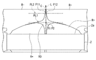
始めに、磁石周辺の磁界の分布を調べた第1のシミュレーションの結果について説明する。第1のシミュレーションでは、有限要素法(FEM)を用いて、磁石2の周辺の磁界の分布を求めた。図10は、第1のシミュレーションによって求めた磁石2の周辺の磁界の分布を示す説明図である。図11は、図10に示した仮想の平面PL1における磁界の分布を示す説明図である。図12は、図10に示した仮想の平面PL2における磁界の分布を示す説明図である。図10は、図11および図12における10−10線の位置における断面を表している。
First, the result of the first simulation in which the magnetic field distribution around the magnet is examined will be described. In the first simulation, the distribution of the magnetic field around the
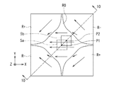
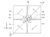
図11および図12において、実線の枠内の矢印は、磁界の方向を表している。また、図10ないし図12において、記号“R+”で示す領域は、角度誤差dθが正の値になる領域を表し、記号“R−”で示す領域は、角度誤差dθが負の値になる領域を表している。また、記号“R0”で示す領域は、角度誤差dθが実質的に0になる領域、すなわち、磁界HSの方向が磁界H0の方向に対してなす角度が実質的に0になる領域(以下、平行磁界領域と言う。)を表している。「角度誤差dθが実質的に0」ならびに「磁界HSの方向が磁界H0の方向に対してなす角度が実質的に0」というのは、角度誤差dθ(磁界HSの方向が磁界H0の方向に対してなす角度)が0の場合の他に、回転角度センサ1における許容範囲内となる場合を含む。なお、図10ないし図12では、便宜上、隣接する領域の境界を線で表している。しかし、実際には、この線を境にして角度誤差dθが不連続に変化するわけではなく、線の近傍では、位置の変化に対して連続的に、ただし急激に、角度誤差dθが変化している。
In FIG. 11 and FIG. 12, the arrow in the solid line frame represents the direction of the magnetic field. 10 to 12, a region indicated by the symbol “R +” represents a region where the angular error dθ has a positive value, and a region indicated by the symbol “R−” has a negative value of the angular error dθ. Represents an area. The region indicated by the symbol “R0” is a region where the angle error dθ is substantially 0, that is, a region where the angle formed by the direction of the magnetic field H S with respect to the direction of the magnetic field H 0 is substantially 0 ( Hereinafter, it is referred to as a parallel magnetic field region). “An angle error dθ is substantially 0” and “an angle formed by the direction of the magnetic field H S with respect to the direction of the magnetic field H 0 is substantially zero” means that the angle error dθ (the direction of the magnetic field H S is the magnetic field H In addition to the case where the angle formed with respect to the direction 0 is 0, the case where the
図10ないし図12から、磁石2の端面2aの近傍には、平行磁界領域R0が存在することと、端面2aに平行な仮想の平面上における平行磁界領域R0の面積は、端面2aと仮想の平面との間の距離によって変化することが分かる。仮想の平面PL1,PL2は、いずれも端面2aに平行な仮想の平面であって、端面2aからの距離が互いに異なる平面である。仮想の平面PL1は、端面2aからの距離を変えて得られる複数の仮想の平面のうち、平行磁界領域R0の面積が最大またはほぼ最大になる平面である。仮想の平面PL2上における平行磁界領域R0の面積は、仮想の平面PL1上における平行磁界領域R0の面積よりも小さい。
10 to 12, the existence of the parallel magnetic field region R0 in the vicinity of the
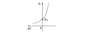
本実施の形態では、仮想の平面PL1と端面2aとの間の距離を最適距離と呼ぶ。ここで、図13を参照して、最適距離の決定方法、すなわち仮想の平面PL1の位置の決定方法について説明する。まず、図10に示したように、回転軸Cに平行な仮想の直線Lを想定する。回転軸Cと直線Lとの間の距離は、例えば、想定される磁石2と磁気センサ5の位置関係のずれ量の最大値程度とし、磁石2の直径d1の0〜10%の範囲内とする。図10に示した例では、磁石2の直径d1は15mmであり、回転軸Cと直線Lとの間の距離は、0.3mmであり、これは、直径d1の2%である。図10および図11において、点P1は、仮想の平面PL1上において回転軸Cが交わる位置を示し、点P2は、仮想の平面PL1上において直線Lが交わる位置を示している。また、図10および図12において、点P11は、仮想の平面PL2上において回転軸Cが交わる位置を示し、点P12は、仮想の平面PL2上において直線Lが交わる位置を示している。
In the present embodiment, the distance between virtual plane PL1 and end
最適距離の決定方法では、次に、直線L上における端面2aからの距離dLと角度誤差dθとの関係を求める。なお、角度誤差dθは、シミュレーションによって得られる直線L上の点における磁界の方向が磁界H0の方向に対してなす角度とする。図13は、距離dLと角度誤差dθとの関係を示している。図13において、横軸は角度誤差dθを示し、縦軸は距離dLを示している。図13における縦軸よりも左側の領域は、角度誤差dθが正の値になる領域を示し、縦軸よりも右側の領域は、角度誤差dθが負の値になる領域を示している。図13に示した例では、距離dLが大きくなるに従って、角度誤差dθは、正の値から負の値に変化している。次に、図13に示した関係から、角度誤差dθが0になる距離dLを求め、これを最適距離dL0とする。なお、仮想の直線Lの位置によっては、図13とは逆に、距離dLが大きくなるに従って、角度誤差dθが負の値から正の値に変化する場合もある。しかし、この場合でも、角度誤差dθが0になる距離dLを求め、これを最適距離dL0とすることができる。
In the optimum distance determination method, the relationship between the distance d L from the
磁石2と磁気センサ5の位置関係のずれに起因した角度誤差dθを小さくするためには、磁気センサ5を仮想の平面PL1上に配置することが好ましい。以下、これについて説明する。図11において、符号5aを付した破線で示す枠は、仮想の平面PL1上において、位置P1と磁気センサ5の中心が一致するように配置された磁気センサ5を表している。符号5aを付した破線で示す枠は、仮想の平面PL1上における磁気センサ5の所望の位置と言える。また、図11において、符号5bを付した破線で示す枠は、仮想の平面PL1上において位置P2と磁気センサ5の中心が一致するように配置された、すなわち所望の位置からずれた位置に配置された磁気センサ5を表している。図12において、符号5cを付した破線で示す枠は、仮想の平面PL2上において位置P11と磁気センサ5の中心が一致するように配置された磁気センサ5を表している。符号5cを付した破線で示す枠は、仮想の平面PL2上における磁気センサ5の所望の位置と言える。また、図12において、符号5dを付した破線で示す枠は、仮想の平面PL2上において位置P12と磁気センサ5の中心が一致するように配置された、すなわち所望の位置からずれた位置に配置された磁気センサ5を表している。
In order to reduce the angular error dθ due to the positional relationship between the
図11に示したように、仮想の平面PL1上では、平行磁界領域R0が広く、符号5aで示した枠(磁気センサ5)と符号5bで示した枠(磁気センサ5)は、共に平行磁界領域R0に含まれている。そのため、磁気センサ5を仮想の平面PL1上に配置した場合には、磁気センサ5が、符号5aで示した所望の位置に配置されていても、符号5bで示した、ずれた位置に配置されていても、角度誤差dθは0になる。
As shown in FIG. 11, the parallel magnetic field region R0 is wide on the virtual plane PL1, and the frame (magnetic sensor 5) indicated by
これに対し、図12に示したように、仮想の平面PL2上では、平行磁界領域R0が狭く、符号5cで示した枠(磁気センサ5)は、ほぼ平行磁界領域R0に含まれているが、符号5dで示した枠(磁気センサ5)内の大きな領域は、平行磁界領域R0に含まれていない。磁気センサ5を仮想の平面PL2上に配置した場合には、磁気センサ5が、符号5cで示した所望の位置に配置されていれば角度誤差dθは0になる。しかし、磁気センサ5が、符号5dで示した、ずれた位置に配置されていると、角度誤差dθは、絶対値の大きな値になる。
On the other hand, as shown in FIG. 12, the parallel magnetic field region R0 is narrow on the virtual plane PL2, and the frame (magnetic sensor 5) indicated by reference numeral 5c is substantially included in the parallel magnetic field region R0. The large region in the frame (magnetic sensor 5) indicated by reference numeral 5d is not included in the parallel magnetic field region R0. When the
以上の説明から理解されるように、磁気センサ5を仮想の平面PL1上に配置することによって、磁石2と磁気センサ5の位置関係のずれに起因した角度誤差dθを小さくすることが可能になる。従って、磁気センサ5を仮想の平面PL1上に配置することが好ましい。仮想の平面PL1上で、回転軸Cが交わる位置P1と、位置P1とは異なる位置P2において、磁石2による磁界の方向は互いに平行である。従って、仮想の平面PL1は、本発明における「磁石の端面と磁気センサとの間の距離と等しい距離だけ端面から離れた位置にあり端面に平行な仮想の平面」に対応し、位置P1は本発明における第1の位置に対応し、位置P2は本発明における第2の位置に対応する。
As can be understood from the above description, by arranging the
なお、本実施の形態における磁石2に限らず、後で比較例の磁石として挙げられる円柱形状の磁石やリング状の磁石の端面の近傍にも、領域R0,R+,R−が存在する。ただし、領域R0,R+,R−の分布は、磁石の形状によって変化する。前述の磁界H0、磁界HS、角度誤差dθおよび最適距離dL0は、比較例の磁石についても用いられる。
Note that the regions R0, R +, and R− are present not only in the
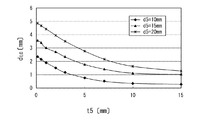
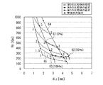
次に、第1の比較例の磁石を用いて磁石の厚みと最適距離dL0との関係を調べた第2のシミュレーションの結果について説明する。第1の比較例の磁石は、磁石2の板状部3と同様の形状を有する円柱形状のネオジボンド磁石である。第2のシミュレーションでは、第1の比較例の磁石の直径と厚みを変化させて、最適距離dL0を求めた。第2のシミュレーションにおけるその他の条件は、第1のシミュレーションと同じである。
Next, the result of a second simulation in which the relationship between the magnet thickness and the optimum distance d L0 is examined using the magnet of the first comparative example will be described. The magnet of the first comparative example is a cylindrical neodybonded magnet having the same shape as the plate-
図14は、第2のシミュレーションによって求めた第1の比較例の磁石の厚みと最適距離dL0との関係を示す特性図である。図14では、第1の比較例の磁石の直径を記号d5で表し、第1の比較例の磁石の厚みを記号t5で表している。図14において、横軸は厚みt5を示し、縦軸は最適距離dL0を示している。図14から、厚みt5が大きくなるに従って、最適距離dL0が小さくなることが分かる。また、直径d5が小さくなるに従って、最適距離dL0が小さくなることが分かる。 FIG. 14 is a characteristic diagram showing the relationship between the thickness of the magnet of the first comparative example and the optimum distance dL0 obtained by the second simulation. In FIG. 14, the diameter of the magnet of the first comparative example is represented by symbol d5, and the thickness of the magnet of the first comparative example is represented by symbol t5. In FIG. 14, the horizontal axis indicates the thickness t5, and the vertical axis indicates the optimum distance dL0 . FIG. 14 shows that the optimum distance dL0 decreases as the thickness t5 increases. Further, according to the diameter d5 is smaller, the optimum distance d L0 becomes It can be seen small.
次に、本実施の形態における磁石2の一例である実施例の磁石2と第2ないし第4の比較例の磁石について、磁石と磁気センサ5との間の距離と磁気センサ5に印加される磁界HSの強度との関係を調べた第3のシミュレーションの結果について説明する。第3のシミュレーションでは、各磁石として、ネオジボンド磁石を用いた。実施例の磁石2の形状は、以下の通りである。直径d1は15mm、空洞4aの直径(リング状部4の内径)d2は4mmである。また、磁石2の厚みt2、板状部3の厚みt3、リング状部4の厚みt4は、それぞれ6mm、3mm、3mmである。
Next, regarding the
第2および第3の比較例の磁石は、磁石2の板状部3と同様の形状を有する円柱形状のネオジボンド磁石である。第4の比較例の磁石は、磁石2のリング状部4と同様の形状を有するネオジボンド磁石である。第2ないし第4の比較例の磁石の直径は、いずれも15mmである。第4の比較例の磁石の空洞の直径(磁石の内径)は4mmである。第2の比較例の磁石の厚みは3mmである。第3および第4の比較例の磁石の厚みは、いずれも6mmである。
The magnets of the second and third comparative examples are cylindrical neodybonded magnets having the same shape as the plate-
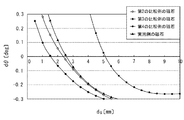
第3のシミュレーションでは、各磁石について、磁石の端面と磁気センサ5との間の距離dGを変化させて、磁気センサ5に印加される磁界HSの強度と角度誤差dθとを求めた。なお、磁界HSの強度は、距離dGだけ磁石の端面から離れた回転軸C上の位置における磁界H0の強度とした。また、角度誤差dθは、距離dGだけ磁石の端面から離れた位置にあり端面に平行な仮想の平面上において、仮想の直線L上における磁界の方向が磁界H0の方向に対してなす角度とした。第3のシミュレーションにおけるその他の条件は、第1のシミュレーションと同じである。
In the third simulation, for each magnet, the strength d of the magnetic field H S applied to the
図15は、第3のシミュレーションによって求めた距離dGと角度誤差dθとの関係を示す特性図である。図16は、第3のシミュレーションによって求めた距離dGと磁気センサ5に印加される磁界HSの強度との関係を示す特性図である。図15において、横軸は距離dGを示し、縦軸は角度誤差dθを示している。図16において、横軸は距離dGを示し、縦軸は磁界HSの強度を示している。磁界HSの強度の単位は、Oe(1Oe=79.6A/m)である。
Figure 15 is a characteristic diagram showing the relationship between the distance d G and angular error dθ obtained by the third simulation. FIG. 16 is a characteristic diagram showing the relationship between the distance d G obtained by the third simulation and the strength of the magnetic field H S applied to the
図15において角度誤差dθが0になる距離dGが最適距離dL0である。最適距離dL0は、実施例の磁石2では約2.5mmであり、第2の比較例の磁石では約2.3mmであり、第3の比較例の磁石では約1.5mmであり、第4の比較例の磁石では約5.1mmである。
In FIG. 15, the distance d G at which the angle error dθ becomes 0 is the optimum distance d L0 . The optimum distance d L0 is about 2.5 mm for the
実施例の磁石2と第2の比較例の磁石とを比較すると、以下のことが分かる。図15に示されるように、実施例の磁石2と第2の比較例の磁石とで、最適距離dL0はほぼ等しい。しかし、図16に示されるように、最適距離dL0における磁界HSの強度は、第2の比較例の磁石に比べて実施例の磁石2の方が大きい。最適距離dL0は、磁石と磁気センサ5の位置関係のずれに起因した角度誤差dθが小さくなるような磁石の端面と磁気センサ5との間の距離である。従って、磁石と磁気センサ5の位置関係のずれに起因した角度誤差dθが小さくなるような磁石の端面と磁気センサ5との間の距離(最適距離dL0)が、ほぼ等しくなる条件で比較すると、本実施の形態における磁石2を用いることにより、円柱形状の磁石(第2の比較例の磁石)を用いる場合に比べて、磁界HSの強度を大きくすることができることが分かる。
When the
第2の比較例の磁石と第3の比較例の磁石とを比較すると、円柱形状の磁石を用いた場合には、磁石の厚みを大きくすると、最適距離dL0における磁界HSの強度は大きくなるものの、最適距離dL0は小さくなることが分かる。従って、円柱形状の磁石を用いた場合には、磁石の厚みを変えることによって、最適距離dL0における磁界の強度を大きくし、且つ磁石と磁気センサ5の位置関係のずれに起因した角度誤差dθを低減しようとすると、磁石と磁気センサ5との間の距離が小さくなりすぎる。
When the magnet of the second comparative example and the magnet of the third comparative example are compared, when a cylindrical magnet is used, the strength of the magnetic field H S at the optimum distance d L0 increases as the magnet thickness increases. However, it can be seen that the optimum distance d L0 is small. Therefore, when a cylindrical magnet is used, the magnetic field strength at the optimum distance d L0 is increased by changing the thickness of the magnet, and the angular error dθ due to the positional relationship between the magnet and the
また、第3の比較例の磁石と第4の比較例の磁石とを比較すると、リング状の磁石(第4の比較例の磁石)を用いることにより、最適距離dL0を大きくすることができることが分かる。しかし、リング状の磁石(第4の比較例の磁石)を用いた場合には、最適距離dL0における磁界HSの強度は非常に小さくなる。 Further, when the magnet of the third comparative example and the magnet of the fourth comparative example are compared, the optimum distance d L0 can be increased by using a ring-shaped magnet (magnet of the fourth comparative example). I understand. However, when a ring-shaped magnet (the magnet of the fourth comparative example) is used, the strength of the magnetic field H S at the optimum distance d L0 is very small.
以上の考察から、本実施の形態における磁石2を用いることにより、磁石2と磁気センサ5との間の距離が小さくなりすぎることなく、磁石2によって発生されて磁気センサ5に印加される磁界の強度を大きくし、且つ磁石2と磁気センサ5の位置関係のずれに起因した角度誤差dθを低減することが可能になることが分かる。この効果は、円柱形状の磁石やリング状の磁石を用いた場合には得ることができない。
From the above consideration, by using the
次に、実施例の磁石2について、最適距離dL0と最適距離dL0における磁界HSの強度との関係を調べた第4のシミュレーションの結果について説明する。第4のシミュレーションにおける実施例の磁石2の形状は、以下の通りである。直径d1は15mm、空洞4aの直径(リング状部4の内径)d2は4mmである。また、磁石2の厚みt2は3mmである。第4のシミュレーションでは、磁石2の厚みt2に対するリング状部4の厚みt4の比率(以下、リング状部分厚み比率と言う。)t4/t2を、0〜100%の範囲内で変化させて、最適距離dL0と、最適距離dL0における磁界HSの強度を求めた。第4のシミュレーションにおけるその他の条件は、第3のシミュレーションと同じである。なお、リング状部分厚み比率が0%の磁石は円柱形状の磁石であり、リング状部分厚み比率が100%の磁石はリング状の磁石である。リング状部分厚み比率が0%の磁石2と100%の磁石2は、本実施の形態における磁石2ではないが、便宜上、実施例の磁石2に含めている。
Next, the result of the fourth simulation in which the relationship between the optimum distance d L0 and the strength of the magnetic field H S at the optimum distance d L0 is examined for the
図17は、第4のシミュレーションによって求めた磁石2のリング状部分厚み比率t4/t2と、最適距離dL0および最適距離dL0における磁界HSの強度との関係を示す特性図である。図17において、横軸はリング状部分厚み比率t4/t2を示し、左側の縦軸は最適距離dL0における磁界HSの強度を示し、右側の縦軸は最適距離dL0を示している。図17から、最適距離dL0は、リング状部分厚み比率t4/t2の一次関数として、リング状部分厚み比率t4/t2の増加に応じて増加することが分かる。また、図17から、最適距離dL0における磁界HSの強度は、リング状部分厚み比率t4/t2の一次関数として、リング状部分厚み比率t4/t2の増加に応じて減少することが分かる。これらのことから理解されるように、本実施の形態によれば、リング状部分厚み比率を調整することによって、最適距離dL0と磁界HSの強度を調整することが可能である。
Figure 17 is a ring-shaped portion thickness ratio t4 / t2 of the
なお、図15および図16を参照して、第3のシミュレーションにおける第2の比較例の磁石と第3の比較例の磁石とを比較すると理解されるように、円柱形状の磁石を用いた場合には、磁石の厚みを小さくすることによって最適距離dL0を大きくしようとすると、本実施の形態における磁石2を用いる場合に比べて、最適距離dL0における磁界HSの強度が小さくなりすぎる。
In addition, with reference to FIG. 15 and FIG. 16, the case where a cylindrical magnet is used as understood when comparing the magnet of the second comparative example and the magnet of the third comparative example in the third simulation If the optimum distance d L0 is increased by reducing the thickness of the magnet, the strength of the magnetic field H S at the optimum distance d L0 becomes too small as compared with the case of using the
前述のように、本実施の形態における磁石2は、リング状部分厚み比率が0%のものと、リング状部分厚み比率が100%のものは含まない。図17に示されるように、本実施の形態では、リング状部分厚み比率が0%よりも大きく100%よりも小さければ、最適距離dL0および最適距離dL0における磁界HSの強度に関して、リング状部分厚み比率が0%または100%の磁石とは異なる特性を有する。従って、本実施の形態における磁石2のリング状部分厚み比率は、0%よりも大きく100%よりも小さければよい。ただし、本実施の形態における磁石2を、リング状部分厚み比率が0%または100%の磁石、すなわち円柱形状またはリング状の磁石と明確に区別するために、本実施の形態における磁石2のリング状部分厚み比率は、5〜95%の範囲内であることが好ましい。
As described above, the
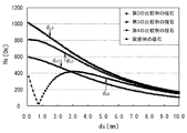
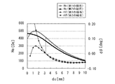
次に、実施例の磁石2と第5ないし第7の比較例の磁石について、磁石の形状と、最適距離dL0および最適距離dL0における磁界HSの強度との関係を調べた第5のシミュレーションの結果について説明する。第5のシミュレーションにおける実施例の磁石2の形状は、以下の通りである。直径d1は15mmである。また、磁石2の厚みt2、板状部3の厚みt3、リング状部4の厚みt4は、それぞれ3mm、1.5mm、1.5mmである。第5ないし第7の比較例の磁石は、磁石2の板状部3と同様の形状を有する円柱形状の磁石であり、それらの直径は、それぞれ10mm、15mm、20mmである。
Next, for the
第5のシミュレーションでは、磁石2の直径d1に対する空洞4aの直径(リング状部4の内径)d2の比率(以下、空洞部分内径比率と言う。)を、0〜100%の範囲内で変化させて、最適距離dL0と、最適距離dL0における磁界HSの強度を求めた。また、第5のシミュレーションでは、第5ないし第7の比較例の磁石の厚みを変化させて、第5ないし第7の比較例の磁石について、最適距離dL0と、最適距離dL0における磁界HSの強度を求めた。第5のシミュレーションにおけるその他の条件は、第3のシミュレーションと同じである。
In the fifth simulation, the ratio of the diameter of the
図18は、第5のシミュレーションによって求めた磁石の形状と、最適距離dL0および最適距離dL0における磁界HSの強度との関係を示す特性図である。図18において、横軸は最適距離dL0を示し、縦軸は最適距離dL0における磁界HSの強度を示している。図18中の各点の近傍に付した数字は、磁石の厚み(単位はmm)を表している。また、符号61は、空洞部分内径比率が0%の点を示し、符号62は、空洞部分内径比率が50%の点を示し、符号63は、空洞部分内径比率が100%の点を示している。空洞部分内径比率が0%の点と50%の点の間の4つの点は、0%の点に近い順に、空洞部分内径比率が10%、20%、30%、40%の点である。また、空洞部分内径比率が50%の点と100%の点の間の4つの点は、50%の点に近い順に、空洞部分内径比率が60%、70%、80%、90%の点である。また、図18において、複数の破線の曲線は、それぞれ、円柱形状の磁石において、厚みを一定にして直径を変化させた場合の特性を表している。特に、符号64を付した破線の曲線は、厚みが3mmの円柱形状の磁石において直径を変化させた場合の特性を表している。また、符号65を付した破線の曲線は、厚みが1.5mmの円柱形状の磁石において直径を変化させた場合の特性を表している。
FIG. 18 is a characteristic diagram showing the relationship between the shape of the magnet obtained by the fifth simulation and the strength of the magnetic field H S at the optimum distance d L0 and the optimum distance d L0 . In FIG. 18, the horizontal axis represents the optimum distance d L0 , and the vertical axis represents the intensity of the magnetic field H S at the optimum distance d L0 . The numbers given in the vicinity of each point in FIG. 18 represent the magnet thickness (unit: mm).
なお、空洞部分内径比率が0%の磁石2は、厚みが3mmの円柱形状の磁石であり、これは、厚みが3mmの第6の比較例の磁石と同じである。また、空洞部分内径比率が100%の磁石2は、厚みが1.5mmの円柱形状の磁石であり、これは、厚みが1.5mmの第6の比較例の磁石と同じである。空洞部分内径比率が0%の磁石2と100%の磁石2は、本実施の形態における磁石2ではないが、便宜上、実施例の磁石2に含めている。
The
図18に示したように、本実施の形態によれば、空洞部分内径比率を調整することによって、最適距離dL0と磁界HSの強度を調整することが可能である。以下、図18に示した第5のシミュレーションの結果から導かれる本実施の形態の効果について説明する。 As shown in FIG. 18, according to the present embodiment, it is possible to adjust the strength of the optimum distance d L0 and the magnetic field H S by adjusting the cavity portion inner diameter ratio. Hereinafter, the effect of the present embodiment derived from the result of the fifth simulation shown in FIG. 18 will be described.
まず、直径が等しい実施例の磁石2と第6の比較例の磁石について、最適距離dL0が等しくなる条件で比較する。すると、図18から、空洞部分内径比率が0%と100%の場合を除いた実施例の磁石2では、第6の比較例の磁石に比べて、最適距離dL0における磁界HSの強度が大きいことが分かる。従って、本実施の形態における磁石2を用いることにより、磁石と磁気センサ5の位置関係のずれに起因した角度誤差dθが小さくなるような磁石の端面と磁気センサ5との間の距離(最適距離dL0)が、ほぼ等しくなる条件で比較すると、円柱形状の磁石(第6の比較例の磁石)を用いる場合に比べて、磁界HSの強度を大きくすることができる。
First, the
次に、実施例の磁石2と第6の比較例の磁石について、最適距離dL0における磁界HSの強度が等しくなる条件で比較する。すると、図18から、空洞部分内径比率が0%と100%の場合を除いた実施例の磁石2では、第6の比較例の磁石に比べて、最適距離dL0が大きいことが分かる。従って、本実施の形態における磁石2を用いることにより、磁界HSの強度がほぼ等しくなる条件で比較すると、円柱形状の磁石(第6の比較例の磁石)を用いる場合に比べて、磁石と磁気センサ5の位置関係のずれに起因した角度誤差dθが小さくなるような磁石の端面と磁気センサ5との間の距離(最適距離dL0)を大きくすることができる。
Next, the
以上のことから、本実施の形態によれば、磁石2と磁気センサ5との間の距離が小さくなりすぎることなく、磁界HSの強度を大きくし、且つ磁石2と磁気センサ5の位置関係のずれに起因した角度誤差dθを低減することが可能になることが分かる。
From the above, according to this embodiment, without the distance between the
前述のように、本実施の形態における磁石2は、空洞部分内径比率が0%のものと、空洞部分内径比率が100%のものは含まない。図18に示されるように、本実施の形態では、空洞部分内径比率が0%よりも大きく100%よりも小さければ、最適距離dL0および最適距離dL0における磁界HSの強度に関して、円柱形状の磁石を用いた場合に比べて効果を発揮する。従って、本実施の形態における磁石2の空洞部分内径比率は、0%よりも大きく100%よりも小さければよい。ただし、本実施の形態における磁石2を、空洞部分内径比率が0%または100%の磁石、すなわち円柱形状の磁石と明確に区別するために、本実施の形態における磁石2の空洞部分内径比率は、5〜95%の範囲内であることが好ましい。
As described above, the
また、図18において、実施例の磁石2の特性を示す曲線のうち、空洞部分内径比率が0%より大きく50%以下の範囲では、特に、以下の効果が顕著に発揮される。すなわち、この範囲では、第6の比較例の磁石の厚みを3mmから1.5mmに小さくすることによって最適距離dL0を大きくする場合に比べて、最適距離dL0を大きくすることができるという効果と最適距離dL0における磁界HSの強度を大きくすることができるという効果が共に顕著に発揮される。従って、これらの顕著な効果を望む場合には、空洞部分内径比率を、0%より大きく50%以下の範囲とすることが好ましく、5〜50%の範囲内とすることがより好ましい。
Further, in FIG. 18, the following effects are remarkably exhibited particularly in the range where the hollow portion inner diameter ratio is larger than 0% and 50% or less in the curve indicating the characteristics of the
また、図18において、実施例の磁石2の特性を示す曲線のうち、空洞部分内径比率が50%より大きく100%より小さい範囲では、空洞部分内径比率を小さくすることにより、最適距離dL0における磁界HSの強度がほとんど変わることなく、最適距離dL0を大きくすることができる。従って、最適距離dL0における磁界HSの強度をほとんど変えることなく、最適距離dL0を調整したい場合には、空洞部分内径比率を、50%より大きく100%より小さい範囲とすることが好ましく、50%より大きく95%以下の範囲内とすることがより好ましい。
Further, in FIG. 18, in the curve indicating the characteristics of the
第5のシミュレーションの結果から導かれる上述の各傾向は、リング状部分厚み比率に依存しない。 Each tendency described above derived from the result of the fifth simulation does not depend on the ring-shaped portion thickness ratio.
以上、第1ないし第5のシミュレーションの結果を参照して説明したように、本実施の形態によれば、磁石2と磁気センサ5との間の距離が小さくなりすぎることなく、磁界HSの強度を大きくし、且つ磁石2と磁気センサ5の位置関係のずれに起因した角度誤差dθを低減することが可能になる。
As described above with reference to the results of the first to fifth simulation, according to the present embodiment, without the distance between the
ところで、図18において、複数の破線の曲線は、円柱形状の磁石において、磁石の直径を大きくことによって、最適距離dL0における磁界HSの強度をあまり減少させずに、最適距離dL0を大きくすることが可能であることを示している。しかし、円柱形状の磁石において、磁石の直径を大きくすると、磁石の体積が大きくなり、その結果、本実施の形態における磁石2に比べて磁石のコストが上昇する。以下、これについて、具体例を挙げて説明する。ここでは、図18を参照して、直径が20mm、厚みが2.8mmの第7の比較例の磁石と、空洞部分内径比率が15%の実施例の磁石2とを比較する。これら2つの磁石では、最適距離dL0はほぼ等しく、最適距離dL0における磁界HSの強度もほぼ等しい。しかし、上記の寸法の第7の比較例の磁石の体積は880mm3であるのに対し、空洞部分内径比率が15%の磁石2の体積は524mm3である。このように、本実施の形態によれば、磁石2を用いることにより、最適距離dL0と最適距離dL0における磁界HSの強度がほぼ等しくなる条件で比較すると、円柱形状の磁石を用いる場合に比べて、磁石2の体積を小さくすることができ、その結果、磁石2のコストを抑制することができる。
By the way, in FIG. 18, a plurality of dashed curves indicate that in a cylindrical magnet, increasing the magnet diameter increases the optimum distance d L0 without significantly reducing the strength of the magnetic field H S at the optimum distance d L0 . It shows that it is possible to do. However, in the cylindrical magnet, when the diameter of the magnet is increased, the volume of the magnet increases, and as a result, the cost of the magnet increases as compared with the
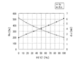
次に、本実施の形態における磁石2について、磁石2と磁気センサ5との間の距離と磁気センサ5に印加される磁界HSの強度との関係を調べた第6のシミュレーションの結果について説明する。第6のシミュレーションでは、最適距離dL0が等しくなるような第1および第2の磁石2を用いた。この2つの磁石の直径d1は15mmであり、厚みt2は3mmである。第1の磁石2では、空洞4aの直径(リング状部4の内径)d2は4mm、リング状部4の厚みt4は1.5mmである。第2の磁石2では、空洞4aの直径(リング状部4の内径)d2は7mm、リング状部4の厚みt4は1mmである。第1の磁石2の体積は511mm3であり、第2の磁石2の体積は492mm3である。第6のシミュレーションでは、第1および第2の磁石2について、磁石2の端面2aと磁気センサ5との間の距離dGを変化させて、磁界HSの強度と角度誤差dθを求めた。なお、第6のシミュレーションにおける磁界HSの強度と角度誤差dθは、第3のシミュレーションで説明した磁界HSの強度と角度誤差dθと同じである。第6のシミュレーションにおけるその他の条件は、第3のシミュレーションと同じである。
Next, the
図19は、第6のシミュレーションによって求めた磁石2と磁気センサ5との間の距離dGと、磁気センサ5に印加される磁界HSの強度および角度誤差dθとの関係を示す特性図である。図19において、横軸は距離dGを示し、左側の縦軸は磁界HSの強度を示し、右側の縦軸は角度誤差dθを示している。また、図19における破線の直線は、第1および第2の磁石2において角度誤差dθが0となる距離dGすなわち最適距離dL0を示している。図19に示されたように、第1の磁石2では、第2の磁石2に比べて、最適距離dL0における磁界HSの強度が大きくなっている。これは、第2の磁石2に比べて、第1の磁石2の体積の方が大きいためと考えられる。この結果から分かるように、磁石2の直径d1および厚みt2を一定にして、リング状部4の内径d2および厚みt4を変えて、同じ最適距離dL0を得る場合には、リング状部4の形状は、内径d2が大きく厚みt4が小さいものよりも、内径d2が小さく厚みt4が大きいものの方が、最適距離dL0における磁界HSの強度を大きくすることができる点で有利である。
Figure 19 is a distance d G between the
以下、本実施の形態におけるその他の効果について説明する。本実施の形態では、磁石2における回転軸Cを含む任意の断面の形状は、回転軸Cに対して線対称な形状である。本実施の形態によれば、このような形状の磁石2を用いることにより、磁石2の形状に起因した角度誤差の発生を防止することができる。上記の形状の要件を満たす磁石2の一例は、ここまで説明してきた磁石2、すなわち板状部3が円板形状を有し、回転軸Cに垂直なリング状部4の任意の断面におけるリング状部4の外周および内周がいずれも円形である磁石2である。しかし、本実施の形態における磁石2は、ここまで説明してきた磁石2に限らず、例えば以下の複数の変形例として挙げられるような種々の形状の磁石を含む。変形例の磁石は、板状部とリング状部とを有し、板状部は回転軸Cが通過する空洞を含まないが、リング状部は回転軸Cが通過する空洞を含んでいる。また、変形例の磁石における回転軸Cを含む任意の断面の形状は回転軸Cに対して線対称な形状である。このような磁石を用いることにより、円柱形状の磁石を用いた場合と比較して、これまでに説明した種々の効果が得ることができる。
Hereinafter, other effects in the present embodiment will be described. In the present embodiment, the shape of an arbitrary cross section including the rotation axis C in the
[変形例]
次に、図20ないし図27を参照して、本実施の形態における磁石2の第1ないし第8の変形例について説明する。図20は、磁石2の第1の変形例を示す平面図である。図21は、磁石2の第2の変形例を示す平面図である。第1および第2の変形例の磁石101は、図1ないし図3に示した磁石2と同様に、回転軸C(図示せず)に垂直な端面101aを有すると共に回転軸Cに垂直な方向の磁化を有している。また、磁石101は、端面101aを含む板状部102と、板状部102に対して端面101aとは反対側に配置されて板状部102に連結されたリング状部(図示せず)とを有している。板状部102は、図20または図21における上下方向に延びた長円板形状(小判形状)を有している。板状部102は、回転軸Cが通過する空洞を含んでいない。リング状部は、外周部と、回転軸Cが通過する空洞とを含んでいる。回転軸Cに垂直なリング状部の任意の断面におけるリング状部の外周の形状は、長円形状(小判形状)であり、これは、回転軸Cに垂直な板状部102の任意の断面における板状部102の外周の形状と同じである。回転軸Cに垂直なリング状部の任意の断面におけるリング状部の内周の形状は、長円形状(小判形状)でもよいし、円形でもよい。
[Modification]
Next, first to eighth modification examples of the
第1の変形例における板状部102は、図20における左右方向に配置されたN極とS極を有している。第2の変形例における板状部102は、図21における上下方向に配置されたN極とS極を有している。第1および第2の変形例の磁石101の磁化の方向は、板状部102のS極からN極に向かう方向であって、S極とN極との境界に垂直な方向である。
The plate-
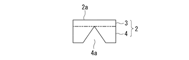
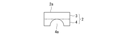
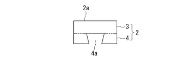
図22ないし図26は、それぞれ、磁石2の第3ないし第7の変形例を示す断面図である。第3ないし第7の変形例の磁石2は、図1ないし図3に示した磁石2と同様に、回転軸C(図示せず)に垂直な端面2aを有すると共に回転軸Cに垂直な方向の磁化を有している。また、第3ないし第7の変形例の磁石2は、端面2aを含む板状部3と、板状部3に対して端面2aとは反対側に配置されて板状部3に連結されたリング状部4とを有している。第3ないし第7の変形例における板状部3の形状は、図1ないし図4に示した板状部3の形状と同じである。図1ないし図3、図5に示したリング状部4と同様に、第3ないし第7の変形例におけるリング状部4は回転軸Cが通過する空洞4aを含んでいる。第3ないし第7の変形例では、回転軸Cに垂直なリング状部4の任意の断面におけるリング状部4の外周および内周はいずれも円形である。
22 to 26 are cross-sectional views showing third to seventh modifications of the
図22ないし図24に示した第3ないし第5の変形例では、リング状部4の内径、すなわち空洞4aの直径は、磁石2の端面2aから離れるに従って大きくなっている。図22に示したように、第3の変形例における空洞4aの形状は、円錐台形状である。図23に示したように、第4の変形例では、板状部3とリング状部4の境界の位置において、リング状部4の内径、すなわち空洞4aの直径は、0である。第4の変形例における空洞4aの形状は、円錐形状である。図24に示したように、第5の変形例における空洞4aの形状は、半球形状である。
In the third to fifth modifications shown in FIGS. 22 to 24, the inner diameter of the ring-shaped
図25に示した第6の変形例では、リング状部4の内径、すなわち空洞4aの直径は、磁石2の端面2aから離れるに従って小さくなっている。図26に示した第7の変形例では、空洞4aのうち、端面2aに近い第1の部分の直径は、端面2aから遠い第2の部分の直径に比べて大きくなっている。第1の部分の直径は、端面2aからの距離によらずに一定である。第2の部分の直径も、端面2aからの距離によらずに一定である。
In the sixth modification shown in FIG. 25, the inner diameter of the ring-shaped
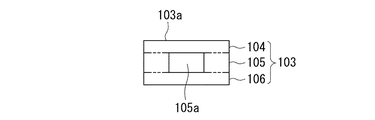
図27は、磁石2の第8の変形例を示す断面図である。第8の変形例の磁石103は、図1ないし図3に示した磁石2と同様に、回転軸C(図示せず)に垂直な端面103aを有すると共に回転軸Cに垂直な方向の磁化を有している。また、磁石103は、端面103aを含む第1の板状部104と、第1の板状部104に対して端面103aとは反対側に配置されて第1の板状部104に連結されたリング状部105と、リング状部105に対して端面103aとは反対側に配置されてリング状部105に連結された第2の板状部106とを有している。第1の板状部104は、本発明における板状部に対応する。第1および第2の板状部104,106は回転軸Cが通過する空洞を含まないが、リング状部105は回転軸Cが通過する空洞105aを含んでいる。第1および第2の板状部104,106は円板形状を有している。回転軸Cに垂直なリング状部105の任意の断面におけるリング状部105の外周および内周はいずれも円形である。第8の変形例では、空洞105aは、第1および第2の板状部104,106とリング状部105によって囲まれている。
FIG. 27 is a cross-sectional view showing an eighth modification of the
本実施の形態における磁石2は、平面形状(端面に垂直な方向から見た形状)が図20または図21に示した形状で、回転軸Cを含む断面の形状が図22ないし図27のいずれかに示した形状のものであってもよい。また、本実施の形態における磁石2は、回転軸Cを含む任意の断面の形状が回転軸Cに対して線対称な形状であればよく、平面形状は正方形、長方形、六角形、八角形等であってもよい。
The
なお、本発明は、上記各実施の形態に限定されず、種々の変更が可能である。例えば、磁気センサ5は、ブリッジ回路16,17における全ての磁気検出素子として、AMR(異方性磁気抵抗効果)素子を用いたものであってもよい。
In addition, this invention is not limited to said each embodiment, A various change is possible. For example, the
1…回転角度センサ、2…磁石、3…板状部、4…リング状部、4a…空洞、5…磁気センサ、6…軸、7…固定用治具、8…基板、11…第1の検出回路、12…第2の検出回路、15…演算回路、16,17…ホイートストンブリッジ回路。
DESCRIPTION OF
Claims (5)
前記磁石の端面に対向して、前記磁石による磁界を検出する磁気センサとを備え、
前記磁気センサの検出出力に基づいて磁石の回転角度を検出する回転角度センサであって、
前記磁石は、
前記端面を含む板状部と、
前記板状部に対して前記端面とは反対側に配置されて前記板状部に連結されたリング状部とを有し、
前記板状部は前記回転軸が通過する空洞を含まないが、前記リング状部は前記回転軸が通過する空洞を含むことを特徴とする回転角度センサ。 A magnet having an end face perpendicular to the rotation axis and having magnetization in a direction perpendicular to the rotation axis, and rotating about the rotation axis;
A magnetic sensor for detecting a magnetic field by the magnet, facing the end face of the magnet,
A rotation angle sensor that detects a rotation angle of a magnet based on a detection output of the magnetic sensor,
The magnet
A plate-like portion including the end face;
A ring-shaped portion disposed on the opposite side of the end surface with respect to the plate-shaped portion and connected to the plate-shaped portion;
The plate-shaped part does not include a cavity through which the rotating shaft passes, but the ring-shaped part includes a cavity through which the rotating shaft passes.
Priority Applications (4)
| Application Number | Priority Date | Filing Date | Title |
|---|---|---|---|
| JP2011003552A JP5141780B2 (en) | 2011-01-12 | 2011-01-12 | Rotation angle sensor |
| US13/301,076 US8749229B2 (en) | 2011-01-12 | 2011-11-21 | Rotation angle sensor |
| DE102012100194A DE102012100194A1 (en) | 2011-01-12 | 2012-01-11 | Rotation angle sensor |
| CN201210022816.5A CN102607405B (en) | 2011-01-12 | 2012-01-12 | Angular sensor |
Applications Claiming Priority (1)
| Application Number | Priority Date | Filing Date | Title |
|---|---|---|---|
| JP2011003552A JP5141780B2 (en) | 2011-01-12 | 2011-01-12 | Rotation angle sensor |
Publications (2)
| Publication Number | Publication Date |
|---|---|
| JP2012145425A JP2012145425A (en) | 2012-08-02 |
| JP5141780B2 true JP5141780B2 (en) | 2013-02-13 |
Family
ID=46454782
Family Applications (1)
| Application Number | Title | Priority Date | Filing Date |
|---|---|---|---|
| JP2011003552A Active JP5141780B2 (en) | 2011-01-12 | 2011-01-12 | Rotation angle sensor |
Country Status (4)
| Country | Link |
|---|---|
| US (1) | US8749229B2 (en) |
| JP (1) | JP5141780B2 (en) |
| CN (1) | CN102607405B (en) |
| DE (1) | DE102012100194A1 (en) |
Cited By (1)
| Publication number | Priority date | Publication date | Assignee | Title |
|---|---|---|---|---|
| US10982974B2 (en) | 2017-04-18 | 2021-04-20 | Tdk Corporation | Magnet, magnet structure, and rotational angle detector |
Families Citing this family (36)
| Publication number | Priority date | Publication date | Assignee | Title |
|---|---|---|---|---|
| KR101371941B1 (en) * | 2011-12-14 | 2014-03-12 | 현대자동차주식회사 | Measurement for angle of constant velocity joint of drive shaft |
| DE102012214916A1 (en) * | 2012-08-22 | 2014-03-20 | Robert Bosch Gmbh | Sensor arrangement for detecting rotational angles on a rotating component |
| JP2014044121A (en) * | 2012-08-27 | 2014-03-13 | Denso Corp | Opening degree detecting device |
| US9606190B2 (en) * | 2012-12-21 | 2017-03-28 | Allegro Microsystems, Llc | Magnetic field sensor arrangements and associated methods |
| JP2014199182A (en) * | 2013-03-29 | 2014-10-23 | Tdk株式会社 | Magnetic sensor system |
| JP2015045529A (en) * | 2013-08-27 | 2015-03-12 | Tdk株式会社 | Revolving magnetic field sensor |
| US9915552B2 (en) * | 2013-11-19 | 2018-03-13 | Infineon Technologies Ag | Perpendicular gradiometric angle sensors, systems and methods |
| DE102014008173B4 (en) * | 2014-06-10 | 2022-08-11 | Tdk-Micronas Gmbh | magnetic field measuring device |
| JP6330178B2 (en) * | 2014-11-19 | 2018-05-30 | 日立金属株式会社 | Torque steering angle sensor |
| JP2016099190A (en) * | 2014-11-20 | 2016-05-30 | アイシン精機株式会社 | Rotation angle detection device |
| DE102015206108A1 (en) * | 2015-04-02 | 2016-10-20 | Bühler Motor GmbH | Magnetic donor funds |
| US9772385B2 (en) * | 2015-04-09 | 2017-09-26 | International Business Machines Corporation | Rotating magnetic field hall measurement system |
| US9678040B2 (en) | 2015-04-09 | 2017-06-13 | International Business Machines Corporation | Rotating magnetic field hall measurement system |
| DE102015105854A1 (en) * | 2015-04-16 | 2016-10-20 | Max Baermann Gmbh | Hall sensor |
| US10139214B2 (en) * | 2015-09-07 | 2018-11-27 | Electronics And Telecommunications Research Institute | Apparatus for acquiring location coordinates of object using two measurement heads and method using the same |
| JP6801170B2 (en) * | 2015-09-10 | 2020-12-16 | 日立金属株式会社 | Manufacturing method of rotation angle detection magnet, rotation angle detection device and rotation angle detection magnet |
| JP6054011B1 (en) * | 2015-11-26 | 2016-12-27 | 三菱電機株式会社 | Magnetic sensor and rotating device |
| DE102016102828B4 (en) * | 2016-02-18 | 2023-04-27 | Infineon Technologies Ag | Magnetic angle sensor device and method |
| JP6512141B2 (en) * | 2016-03-09 | 2019-05-15 | Tdk株式会社 | Magnet and displacement detection device |
| JP6278050B2 (en) * | 2016-03-11 | 2018-02-14 | Tdk株式会社 | Rotation angle detection device and rotary machine device |
| CN107607036A (en) * | 2016-07-12 | 2018-01-19 | 吕方达 | Swing mechanism |
| JP6671269B2 (en) * | 2016-09-21 | 2020-03-25 | アルプスアルパイン株式会社 | Rotary input device |
| US10591274B2 (en) * | 2016-09-28 | 2020-03-17 | Infineon Technologies Ag | External field robust angle sensing with differential magnetic field |
| WO2018198235A1 (en) * | 2017-04-26 | 2018-11-01 | 三菱電機株式会社 | Rotary actuator and vg actuator |
| CN108953596A (en) * | 2017-05-18 | 2018-12-07 | 泰科电子(上海)有限公司 | For sensing the sensor-based system of gear rotating shaft position |
| DE102017121467A1 (en) * | 2017-09-15 | 2019-03-21 | Infineon Technologies Ag | MAGNETIC SENSOR COMPONENT AND METHOD FOR DETERMINING A ROTATIONAL SPEED, A ROTATIONAL DIRECTION, AND / OR A ROTATION ANGLE OF A MAGNETIC COMPONENT FOR A ROTATIONAL AXIS |
| DE102017216664A1 (en) * | 2017-09-20 | 2019-03-21 | Continental Teves Ag & Co. Ohg | Electric hollow shaft motor |
| JP6796573B2 (en) * | 2017-11-17 | 2020-12-09 | 日本電産モビリティ株式会社 | Magnetic pole direction detector |
| JP7151105B2 (en) * | 2018-03-08 | 2022-10-12 | Tdk株式会社 | Magnet structure, rotation angle detector, and electric power steering device |
| JP6954187B2 (en) * | 2018-03-08 | 2021-10-27 | Tdk株式会社 | Magnet structure, rotation angle detector and electric power steering device |
| JP7001513B2 (en) * | 2018-03-22 | 2022-01-19 | 株式会社東海理化電機製作所 | Magnetic sensor |
| JP6784283B2 (en) | 2018-09-19 | 2020-11-11 | Tdk株式会社 | Angle sensor system |
| CN111664778B (en) * | 2019-03-06 | 2021-10-26 | 英飞凌科技股份有限公司 | External field robust angle sensing using differential magnetic fields |
| HUE059648T2 (en) | 2019-03-15 | 2022-12-28 | Bourns Inc | Vehicle with steering angle sensor |
| WO2022004227A1 (en) * | 2020-07-03 | 2022-01-06 | 株式会社村田製作所 | Position detecting device |
| JP7453166B2 (en) * | 2021-01-26 | 2024-03-19 | ヒロセ電機株式会社 | rotation detection device |
Family Cites Families (13)
| Publication number | Priority date | Publication date | Assignee | Title |
|---|---|---|---|---|
| JP2002022406A (en) * | 2000-07-11 | 2002-01-23 | Yazaki Corp | Rotation angle sensor |
| JP4259937B2 (en) * | 2003-06-30 | 2009-04-30 | アルプス電気株式会社 | Angle detection sensor |
| JP2006208048A (en) * | 2005-01-25 | 2006-08-10 | Denso Corp | Rotation angle detection apparatus |
| JP4947250B2 (en) * | 2005-01-31 | 2012-06-06 | Tdk株式会社 | Angle detector |
| JP4955244B2 (en) | 2005-09-27 | 2012-06-20 | 横河電機株式会社 | Biochip reader and biochip reader method |
| JP2007093280A (en) | 2005-09-27 | 2007-04-12 | Asahi Kasei Electronics Co Ltd | Rotation angle sensor |
| JP2007093284A (en) | 2005-09-27 | 2007-04-12 | Denso Corp | Car navigation system |
| JP5021253B2 (en) * | 2006-08-24 | 2012-09-05 | 株式会社デンソー | Rotation angle detector |
| JP5105201B2 (en) * | 2008-07-30 | 2012-12-26 | Tdk株式会社 | Angle detection apparatus and angle detection method |
| JP5330930B2 (en) * | 2008-09-05 | 2013-10-30 | 日本電産サンキョー株式会社 | Magnetic rotation detection device and manufacturing method thereof |
| JP5137755B2 (en) | 2008-09-12 | 2013-02-06 | 古河電気工業株式会社 | Rotation sensor |
| JP2010145371A (en) * | 2008-12-22 | 2010-07-01 | Aisin Seiki Co Ltd | Angle detection apparatus |
| JP5202343B2 (en) * | 2009-01-08 | 2013-06-05 | 三菱電機株式会社 | Rotation angle detector |
-
2011
- 2011-01-12 JP JP2011003552A patent/JP5141780B2/en active Active
- 2011-11-21 US US13/301,076 patent/US8749229B2/en active Active
-
2012
- 2012-01-11 DE DE102012100194A patent/DE102012100194A1/en active Pending
- 2012-01-12 CN CN201210022816.5A patent/CN102607405B/en active Active
Cited By (1)
| Publication number | Priority date | Publication date | Assignee | Title |
|---|---|---|---|---|
| US10982974B2 (en) | 2017-04-18 | 2021-04-20 | Tdk Corporation | Magnet, magnet structure, and rotational angle detector |
Also Published As
| Publication number | Publication date |
|---|---|
| CN102607405B (en) | 2015-11-25 |
| US8749229B2 (en) | 2014-06-10 |
| JP2012145425A (en) | 2012-08-02 |
| CN102607405A (en) | 2012-07-25 |
| US20120176126A1 (en) | 2012-07-12 |
| DE102012100194A1 (en) | 2012-07-12 |
Similar Documents
| Publication | Publication Date | Title |
|---|---|---|
| JP5141780B2 (en) | Rotation angle sensor | |
| JP5062450B2 (en) | Rotating magnetic field sensor | |
| JP5590349B2 (en) | Magnetic sensor system | |
| CN101587174B (en) | Magnetic sensor | |
| JP5062449B2 (en) | Rotating magnetic field sensor | |
| US11371863B2 (en) | Rotational angle detection apparatus and rotating machine apparatus | |
| JP5843079B2 (en) | Magnetic sensor and magnetic sensor system | |
| JP5297539B2 (en) | Magnetic sensor | |
| JP5062454B2 (en) | Magnetic sensor | |
| JP5464237B2 (en) | Magnetic sensor | |
| JP6319348B2 (en) | Rotation angle detector | |
| US20180313670A1 (en) | Magnetism-detecting device and moving-body-detecting device | |
| JP2015219227A (en) | Magnetic sensor | |
| JP6066134B2 (en) | Magnetic sensor system | |
| JP2016166748A (en) | Magnetic sensor | |
| JP6784283B2 (en) | Angle sensor system | |
| JP5062453B2 (en) | Magnetic sensor | |
| JP2005321272A (en) | Magnetostrictive torque sensor | |
| JP2023088219A (en) | Angle sensor device and angle detection device | |
| JP2010002293A (en) | Potentiometer | |
| JP2010133882A (en) | Absolute position detector | |
| JP2012119518A (en) | Rotation angle sensor | |
| JP2008298632A (en) | Rotation angle detector and method of detecting rotational angle |
Legal Events
| Date | Code | Title | Description |
|---|---|---|---|
| A977 | Report on retrieval |
Free format text: JAPANESE INTERMEDIATE CODE: A971007 Effective date: 20121002 |
|
| TRDD | Decision of grant or rejection written | ||
| A01 | Written decision to grant a patent or to grant a registration (utility model) |
Free format text: JAPANESE INTERMEDIATE CODE: A01 Effective date: 20121023 |
|
| A01 | Written decision to grant a patent or to grant a registration (utility model) |
Free format text: JAPANESE INTERMEDIATE CODE: A01 |
|
| A61 | First payment of annual fees (during grant procedure) |
Free format text: JAPANESE INTERMEDIATE CODE: A61 Effective date: 20121105 |
|
| FPAY | Renewal fee payment (event date is renewal date of database) |
Free format text: PAYMENT UNTIL: 20151130 Year of fee payment: 3 |
|
| R150 | Certificate of patent or registration of utility model |
Ref document number: 5141780 Country of ref document: JP Free format text: JAPANESE INTERMEDIATE CODE: R150 Free format text: JAPANESE INTERMEDIATE CODE: R150 |