JP5132306B2 - Light scattering EUVL mask - Google Patents
Light scattering EUVL mask Download PDFInfo
- Publication number
- JP5132306B2 JP5132306B2 JP2007515303A JP2007515303A JP5132306B2 JP 5132306 B2 JP5132306 B2 JP 5132306B2 JP 2007515303 A JP2007515303 A JP 2007515303A JP 2007515303 A JP2007515303 A JP 2007515303A JP 5132306 B2 JP5132306 B2 JP 5132306B2
- Authority
- JP
- Japan
- Prior art keywords
- crystalline silicon
- silicon layer
- ultraviolet
- mask
- multilayer
- Prior art date
- Legal status (The legal status is an assumption and is not a legal conclusion. Google has not performed a legal analysis and makes no representation as to the accuracy of the status listed.)
- Expired - Fee Related
Links
- 238000001900 extreme ultraviolet lithography Methods 0.000 title claims description 40
- 238000000149 argon plasma sintering Methods 0.000 title claims description 11
- 229910021419 crystalline silicon Inorganic materials 0.000 claims description 49
- 230000005855 radiation Effects 0.000 claims description 44
- 238000000034 method Methods 0.000 claims description 42
- 239000004065 semiconductor Substances 0.000 claims description 26
- 238000007639 printing Methods 0.000 claims description 23
- 239000000758 substrate Substances 0.000 claims description 20
- XUIMIQQOPSSXEZ-UHFFFAOYSA-N Silicon Chemical compound [Si] XUIMIQQOPSSXEZ-UHFFFAOYSA-N 0.000 claims description 16
- 229910052710 silicon Inorganic materials 0.000 claims description 16
- 239000010703 silicon Substances 0.000 claims description 16
- 238000000151 deposition Methods 0.000 claims description 15
- 238000004519 manufacturing process Methods 0.000 claims description 15
- 239000000463 material Substances 0.000 claims description 12
- ZOKXTWBITQBERF-UHFFFAOYSA-N Molybdenum Chemical compound [Mo] ZOKXTWBITQBERF-UHFFFAOYSA-N 0.000 claims description 9
- 229910052750 molybdenum Inorganic materials 0.000 claims description 9
- 239000011733 molybdenum Substances 0.000 claims description 9
- 229920002120 photoresistant polymer Polymers 0.000 claims description 9
- 230000003287 optical effect Effects 0.000 claims description 8
- 238000005530 etching Methods 0.000 claims description 7
- 238000007493 shaping process Methods 0.000 claims description 5
- 235000012431 wafers Nutrition 0.000 description 42
- 239000006096 absorbing agent Substances 0.000 description 9
- 238000012545 processing Methods 0.000 description 8
- WGTYBPLFGIVFAS-UHFFFAOYSA-M tetramethylammonium hydroxide Chemical compound [OH-].C[N+](C)(C)C WGTYBPLFGIVFAS-UHFFFAOYSA-M 0.000 description 8
- 238000010521 absorption reaction Methods 0.000 description 6
- 238000001020 plasma etching Methods 0.000 description 6
- 230000008569 process Effects 0.000 description 6
- 230000004048 modification Effects 0.000 description 5
- 238000012986 modification Methods 0.000 description 5
- 238000002310 reflectometry Methods 0.000 description 5
- 238000001039 wet etching Methods 0.000 description 5
- 230000000694 effects Effects 0.000 description 4
- 239000013078 crystal Substances 0.000 description 3
- 238000001459 lithography Methods 0.000 description 3
- 239000010453 quartz Substances 0.000 description 3
- 230000009467 reduction Effects 0.000 description 3
- VYPSYNLAJGMNEJ-UHFFFAOYSA-N silicon dioxide Inorganic materials O=[Si]=O VYPSYNLAJGMNEJ-UHFFFAOYSA-N 0.000 description 3
- 238000012876 topography Methods 0.000 description 3
- KWYUFKZDYYNOTN-UHFFFAOYSA-M Potassium hydroxide Chemical compound [OH-].[K+] KWYUFKZDYYNOTN-UHFFFAOYSA-M 0.000 description 2
- 230000006978 adaptation Effects 0.000 description 2
- 239000012670 alkaline solution Substances 0.000 description 2
- 230000008901 benefit Effects 0.000 description 2
- ONRPGGOGHKMHDT-UHFFFAOYSA-N benzene-1,2-diol;ethane-1,2-diamine Chemical compound NCCN.OC1=CC=CC=C1O ONRPGGOGHKMHDT-UHFFFAOYSA-N 0.000 description 2
- 238000004140 cleaning Methods 0.000 description 2
- 238000003384 imaging method Methods 0.000 description 2
- 238000007689 inspection Methods 0.000 description 2
- 238000000059 patterning Methods 0.000 description 2
- 230000008439 repair process Effects 0.000 description 2
- 238000007788 roughening Methods 0.000 description 2
- 239000000243 solution Substances 0.000 description 2
- 230000007704 transition Effects 0.000 description 2
- XLYOFNOQVPJJNP-UHFFFAOYSA-N water Substances O XLYOFNOQVPJJNP-UHFFFAOYSA-N 0.000 description 2
- 238000000347 anisotropic wet etching Methods 0.000 description 1
- 238000004380 ashing Methods 0.000 description 1
- 230000005540 biological transmission Effects 0.000 description 1
- 230000015572 biosynthetic process Effects 0.000 description 1
- 239000006227 byproduct Substances 0.000 description 1
- 238000006243 chemical reaction Methods 0.000 description 1
- 230000008021 deposition Effects 0.000 description 1
- 238000013461 design Methods 0.000 description 1
- 238000010586 diagram Methods 0.000 description 1
- 238000001312 dry etching Methods 0.000 description 1
- 238000005516 engineering process Methods 0.000 description 1
- 238000002474 experimental method Methods 0.000 description 1
- 238000010438 heat treatment Methods 0.000 description 1
- 238000005286 illumination Methods 0.000 description 1
- 230000006872 improvement Effects 0.000 description 1
- 230000000873 masking effect Effects 0.000 description 1
- 239000012528 membrane Substances 0.000 description 1
- GALOTNBSUVEISR-UHFFFAOYSA-N molybdenum;silicon Chemical compound [Mo]#[Si] GALOTNBSUVEISR-UHFFFAOYSA-N 0.000 description 1
- 230000001681 protective effect Effects 0.000 description 1
- 230000007261 regionalization Effects 0.000 description 1
- 239000007787 solid Substances 0.000 description 1
- 239000000126 substance Substances 0.000 description 1
- 230000003746 surface roughness Effects 0.000 description 1
- 238000012546 transfer Methods 0.000 description 1
Images


Classifications
-
- G—PHYSICS
- G03—PHOTOGRAPHY; CINEMATOGRAPHY; ANALOGOUS TECHNIQUES USING WAVES OTHER THAN OPTICAL WAVES; ELECTROGRAPHY; HOLOGRAPHY
- G03F—PHOTOMECHANICAL PRODUCTION OF TEXTURED OR PATTERNED SURFACES, e.g. FOR PRINTING, FOR PROCESSING OF SEMICONDUCTOR DEVICES; MATERIALS THEREFOR; ORIGINALS THEREFOR; APPARATUS SPECIALLY ADAPTED THEREFOR
- G03F1/00—Originals for photomechanical production of textured or patterned surfaces, e.g., masks, photo-masks, reticles; Mask blanks or pellicles therefor; Containers specially adapted therefor; Preparation thereof
- G03F1/22—Masks or mask blanks for imaging by radiation of 100nm or shorter wavelength, e.g. X-ray masks, extreme ultraviolet [EUV] masks; Preparation thereof
- G03F1/24—Reflection masks; Preparation thereof
-
- G—PHYSICS
- G21—NUCLEAR PHYSICS; NUCLEAR ENGINEERING
- G21K—TECHNIQUES FOR HANDLING PARTICLES OR IONISING RADIATION NOT OTHERWISE PROVIDED FOR; IRRADIATION DEVICES; GAMMA RAY OR X-RAY MICROSCOPES
- G21K1/00—Arrangements for handling particles or ionising radiation, e.g. focusing or moderating
- G21K1/06—Arrangements for handling particles or ionising radiation, e.g. focusing or moderating using diffraction, refraction or reflection, e.g. monochromators
- G21K1/062—Devices having a multilayer structure
-
- B—PERFORMING OPERATIONS; TRANSPORTING
- B82—NANOTECHNOLOGY
- B82Y—SPECIFIC USES OR APPLICATIONS OF NANOSTRUCTURES; MEASUREMENT OR ANALYSIS OF NANOSTRUCTURES; MANUFACTURE OR TREATMENT OF NANOSTRUCTURES
- B82Y10/00—Nanotechnology for information processing, storage or transmission, e.g. quantum computing or single electron logic
-
- B—PERFORMING OPERATIONS; TRANSPORTING
- B82—NANOTECHNOLOGY
- B82Y—SPECIFIC USES OR APPLICATIONS OF NANOSTRUCTURES; MEASUREMENT OR ANALYSIS OF NANOSTRUCTURES; MANUFACTURE OR TREATMENT OF NANOSTRUCTURES
- B82Y40/00—Manufacture or treatment of nanostructures
-
- G—PHYSICS
- G03—PHOTOGRAPHY; CINEMATOGRAPHY; ANALOGOUS TECHNIQUES USING WAVES OTHER THAN OPTICAL WAVES; ELECTROGRAPHY; HOLOGRAPHY
- G03F—PHOTOMECHANICAL PRODUCTION OF TEXTURED OR PATTERNED SURFACES, e.g. FOR PRINTING, FOR PROCESSING OF SEMICONDUCTOR DEVICES; MATERIALS THEREFOR; ORIGINALS THEREFOR; APPARATUS SPECIALLY ADAPTED THEREFOR
- G03F1/00—Originals for photomechanical production of textured or patterned surfaces, e.g., masks, photo-masks, reticles; Mask blanks or pellicles therefor; Containers specially adapted therefor; Preparation thereof
- G03F1/38—Masks having auxiliary features, e.g. special coatings or marks for alignment or testing; Preparation thereof
-
- G—PHYSICS
- G21—NUCLEAR PHYSICS; NUCLEAR ENGINEERING
- G21K—TECHNIQUES FOR HANDLING PARTICLES OR IONISING RADIATION NOT OTHERWISE PROVIDED FOR; IRRADIATION DEVICES; GAMMA RAY OR X-RAY MICROSCOPES
- G21K2201/00—Arrangements for handling radiation or particles
- G21K2201/06—Arrangements for handling radiation or particles using diffractive, refractive or reflecting elements
- G21K2201/067—Construction details
Description
本発明は、一般的に、反射マスクに関し、より詳細には、光散乱・放射反射EUVLマスクに関する。 The present invention relates generally to reflective masks and, more particularly, to light scattering and radiation reflective EUVL masks.
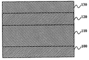
半導体産業全体にわたってウェハに像を形成する(image)ために使用される光リソグラフィ技術は、透明なマスクに依拠してマスクからウェハに像を転写する。ウェハの像が小さくなるので、ウェハのレジストに像を形成する新しい方法が必要とされている。次世代リソグラフィの1つの有望な候補では、像形成のために極端紫外(EUV)光が使用される。13.4nmのEUV波長では、材料は余りにも吸収が高すぎて透過マスクを作ることができないので、代わりに反射マスクが使用される。図1に示すマスクのような従来の極端紫外リソグラフィ(EUVL)・マスクは、超低膨張(ULE)基板10に反射膜を堆積することによって作られる。ULE基板の材料特性は、当技術分野でよく知られている。この膜は、多くの異なる材料で構成されることがある。EUVLマスク用途に最も一般的に採用される反射ブラッグ・ミラーは、モリブデン(Mo)とシリコン(Si)の多数(40以上くらい)の交互二層で作られ、Mo/Si多層20としてひとまとめにして示されている保護Siキャップで終わっている。それからバッファ層30および吸収層40が、多層スタック20に堆積される。エッチング停止層または導電性検査/リペア層を設けるためなどの様々な目的のために、キャップ/バッファ/吸収体スタックの中のどこにでも追加の層を堆積することができる。マスク・パターンは、標準的なマスク・パターン形成プロセスを使用してレジスト層に描画される。ドライ・エッチングで、吸収層を通してパターンが転写される。吸収体のパターンが確実に設計データと一致するように、検査およびリペアが行われ、そして最終パターンがバッファ層を通して転写されて、反射多層表面を露出させる。
Photolithographic techniques used to image the wafer throughout the semiconductor industry rely on a transparent mask to transfer the image from the mask to the wafer. As wafer images become smaller, there is a need for new methods of forming images on wafer resist. One promising candidate for next generation lithography uses extreme ultraviolet (EUV) light for imaging. At the EUV wavelength of 13.4 nm, the material is too absorbing to make a transmission mask, so a reflective mask is used instead. A conventional extreme ultraviolet lithography (EUVL) mask, such as the mask shown in FIG. 1, is made by depositing a reflective film on an ultra-low expansion (ULE)
EUVLマスクの製作および使用に固有の多くの材料的な問題がある。1つの基本的なマスク問題は、理想的な化学的な耐久性、付着性、ドライ・エッチング特性、およびオプティカル(optical)を兼ね備える吸収材料およびバッファ材料を選ぶことである。さらに、マスク処理中にキャップ層の反射表面の品質(したがって、反射率)を維持することは、困難である。 There are a number of material problems inherent in the manufacture and use of EUVL masks. One basic mask problem is to choose an absorbing and buffer material that combines ideal chemical durability, adhesion, dry etch properties, and optical. Furthermore, it is difficult to maintain the quality (and thus reflectivity) of the reflective surface of the cap layer during masking.
一般に、従来の光マスクは、光がウェハに通過することができるようにする透過領域と、光を遮断する吸収領域とを含む。しかし、EUVLシステムで使用されるマスクは、一組の新しい問題を生じる。EUVLマスクは反射性であるので、パターンがウェハの表面に反射するような角度で、EUV放射がマスク表面に向いていなければならない。具体的には、露出した反射表面に入射する光が反射される。パターン形成された吸収膜に入射した光は、吸収され、反射されない。これは、像形成にとって本質的な構成要素である。この吸収の副産物は、放射によってマスクが加熱され、それで、パターン歪みを起さないようにかつマスク寿命を短くするかもしれない熱による損耗を制限するように、放射を制御しなればならないことである。実験で、5度が露光の最適角度であることが明らかになった。 In general, conventional optical masks include a transmissive region that allows light to pass through the wafer and an absorbing region that blocks the light. However, the masks used in EUVL systems create a new set of problems. Since the EUVL mask is reflective, the EUV radiation must be directed to the mask surface at an angle such that the pattern reflects to the wafer surface. Specifically, light incident on the exposed reflective surface is reflected. Light incident on the patterned absorption film is absorbed and not reflected. This is an essential component for imaging. A by-product of this absorption is that the mask must be controlled by radiation so that it does not cause pattern distortion and limits thermal wear that may shorten mask life. is there. Experiments have shown that 5 degrees is the optimum angle of exposure.
吸収スタックの高さは、有限であり、照明の角度のもとで影を生じ、この影は、像が形成されたとき、高い吸収体の縁をぼやかす。このコントラストの低下は、入射露光光の角度と、吸収層およびバッファ層の両方の厚さとの関数である。パターンの縁のコントラストの低下は、結果として、シフトした像または間違った大きさの像をウェハ上に生じることがあるので、重大な問題である。
業界は、これらの特定された問題を克服しようと努めてきたが、まだ解決策は適切に確定されていない。したがって、従来のデバイスおよびプロセスの限界のために、標準技術に関連した問題を克服する新規なEUVLマスクが必要とされている。 The industry has sought to overcome these identified problems, but a solution has not yet been properly established. Therefore, due to limitations of conventional devices and processes, new EUVL masks that overcome the problems associated with standard technology are needed.
本発明は、マスク・スタックのバッファ層と吸収層の両方を完全になくすることによって、上に特定された問題を克服する。本発明は、光散乱極端紫外リソグラフィ・マスクを提供し、このマスクでは、露光光がウェハに当たるように予定された領域でEUV放射を反射し、かつ露光光がウェハに達するように予定されていない領域で散乱させる特定のトポグラフィでパターン形成されたブランクの上に、シリコン・モリブデン多層が堆積されている。光をウェハに反射するように予定された領域のトポグラフィは、平らな領域として形作られている。しかし、EUV放射がウェハの表面に達するように予定されていない領域では、トポグラフィは、ステッパの像形成光学系(optics)の範囲外に放射を散乱させるように形作られており、したがって印刷しないであろう。 The present invention overcomes the problems identified above by completely eliminating both the buffer layer and the absorber layer of the mask stack. The present invention provides a light scattering extreme ultraviolet lithography mask that reflects EUV radiation in an area where exposure light is intended to strike the wafer and is not intended for exposure light to reach the wafer. A silicon-molybdenum multilayer is deposited on a blank patterned with a particular topography that scatters in the region. The topography of the area planned to reflect light to the wafer is shaped as a flat area. However, in areas where EUV radiation is not scheduled to reach the surface of the wafer, the topography is shaped to scatter the radiation out of range of the stepper's optics, and therefore should not be printed. I will.
具体的には、本発明は、紫外線反射領域および紫外線散乱領域を備える極端紫外リソグラフィ・マスクを提供し、反射領域および散乱領域は同じ材料で構成されている。反射領域は、モリブデンとシリコンの多層を備え、この多層は、半導体ウェハに像を形成するように入射紫外放射波を反射するように形作られた平らな表面を備える。散乱領域は、モリブデンとシリコンの多層を備え、この多層は、露光光学系による集光(collection)を妨げ/避けかつ半導体ウェハへの像形成を妨げるように入射紫外放射波を偏向させるように選ばれた角度で形作られた1つまたは複数の斜面を備え、この角度は、露光光学系の集光角よりも大きい。他の実施形態では、散乱領域は、露光光学系による集光を妨げ/避けかつ半導体ウェハへの印刷を妨げるように入射紫外放射波を偏向させるように形作られた粗面、ぎざぎざの表面、または曲面を備える。 Specifically, the present invention provides an extreme ultraviolet lithography mask comprising an ultraviolet reflective region and an ultraviolet scattering region, where the reflective region and the scattering region are composed of the same material. The reflective region comprises a multilayer of molybdenum and silicon, which comprises a flat surface shaped to reflect incident ultraviolet radiation so as to form an image on a semiconductor wafer. The scattering region comprises a multilayer of molybdenum and silicon, which is selected to deflect incident ultraviolet radiation so as to prevent / avoid collection by the exposure optics and prevent image formation on the semiconductor wafer. One or more slopes formed at a defined angle, which is greater than the collection angle of the exposure optics. In other embodiments, the scattering region is a rough surface, a jagged surface, or a jagged surface shaped to deflect incident ultraviolet radiation so as to prevent / avoid collection by the exposure optics and prevent printing on a semiconductor wafer. It has a curved surface.
さらに、本発明は、超低膨張基板と、この超低膨張基板の上の結晶シリコン層と、この結晶シリコン層の上のモリブデンとシリコンを含む放射反射・光散乱多層とを備える光散乱反射マスクを提供する。この多層は、下のシリコン層に整合して、水平部分および平坦でない部分を有している。水平部分は、入射紫外放射波を半導体ウェハに反射するように形作られている。一実施形態では、平坦でない部分は、光が半導体ウェハに達するのを妨げるように入射紫外放射波を偏向させる角度で配置された傾斜した外形を備えている。他の実施形態では、平坦でない部分は、露光光学系による集光を妨げ/避けかつ半導体ウェハへの印刷を妨げるように入射紫外放射波を偏向させるように形作られた粗面を備える。さらに他の実施形態では、平坦でない部分は、露光光学系による集光を妨げ/避けかつ半導体ウェハへの印刷を妨げるように入射紫外放射波を偏向させるように形作られたぎざぎざの表面を備える。代わりに、平坦でない部分は、露光光学系による集光を妨げ/避けかつ半導体ウェハへの印刷を妨げるように入射紫外放射波を偏向させるように形作られた曲面を備える。 Furthermore, the present invention provides a light scattering reflection mask comprising an ultra low expansion substrate, a crystalline silicon layer on the ultra low expansion substrate, and a radiation reflection / light scattering multilayer containing molybdenum and silicon on the crystalline silicon layer I will provide a. This multilayer has horizontal and non-planar portions in alignment with the underlying silicon layer. The horizontal portion is shaped to reflect incident ultraviolet radiation to the semiconductor wafer. In one embodiment, the non-planar portion comprises a sloping profile arranged at an angle that deflects the incident ultraviolet radiation to prevent light from reaching the semiconductor wafer. In other embodiments, the non-planar portion comprises a rough surface shaped to deflect incident ultraviolet radiation so as to prevent / avoid collection by the exposure optics and prevent printing onto the semiconductor wafer. In yet other embodiments, the non-planar portion comprises a jagged surface shaped to deflect incident ultraviolet radiation so as to prevent / avoid collection by the exposure optics and prevent printing onto the semiconductor wafer. Instead, the non-planar part comprises a curved surface shaped to deflect incident ultraviolet radiation so as to prevent / avoid focusing by the exposure optics and prevent printing on the semiconductor wafer.
本発明の他の態様は、超低膨張基板の上に結晶シリコン層を陽極接合し、それからこの結晶シリコン層の上にモリブデンとシリコンを含む共形の多層を堆積することによって、極端紫外リソグラフィ・マスクを形成する方法を提供する。この多層は、光をウェハに反射する水平部分と、ウェハに当たらないように光を散乱させる平坦でない部分とを備える。反射多層を堆積するステップより前に、本方法は、さらに、結晶シリコン層の上にハードマスクを堆積すること、ハードマスクの上にフォトレジスト・マスクを堆積すること、フォトレジストでパターンを作ること、および、このパターンをハードマスクに転写することを含む。本方法は、さらに、結晶シリコン層のエッチングされた領域に平坦でない表面を生成するように結晶シリコン層をエッチングすること、およびハードマスクを除去することを含む。その上、プラズマ・エッチングを使用して、パターンは、ハードマスクに転写され、ここで、結晶シリコンのエッチングは異方性エッチングを含み、この異方性エッチングは、水酸化カリウム(KOH)水、水酸化テトラメチルアンモニウム(TMAH)、またはエチレンジアミン・パイロカテコール(EDP)のようなアルカリ溶液を使用して行われる。さらに、このエッチングは、結晶シリコン層の<100>格子面に沿って行われる。 Another aspect of the present invention is an extreme ultraviolet lithography process by anodic bonding a crystalline silicon layer on an ultra-low expansion substrate and then depositing a conformal multilayer comprising molybdenum and silicon on the crystalline silicon layer. A method of forming a mask is provided. The multilayer includes a horizontal portion that reflects light to the wafer and an uneven portion that scatters light so that it does not strike the wafer. Prior to the step of depositing the reflective multilayer, the method further comprises depositing a hard mask over the crystalline silicon layer, depositing a photoresist mask over the hard mask, and patterning with the photoresist. And transferring this pattern to a hard mask. The method further includes etching the crystalline silicon layer to produce a non-planar surface in the etched region of the crystalline silicon layer, and removing the hard mask. In addition, using plasma etching, the pattern is transferred to a hard mask, where the etching of crystalline silicon includes anisotropic etching, which includes potassium hydroxide (KOH) water, It is performed using an alkaline solution such as tetramethylammonium hydroxide (TMAH) or ethylenediamine pyrocatechol (EDP). Further, this etching is performed along the <100> lattice plane of the crystalline silicon layer.
さらに、水平領域は、半導体ウェハに印刷するために入射紫外放射波を反射するように形作られ、第1の実施形態では、平坦でない領域は、下の結晶シリコン層に共形的な斜面を備え、この斜面は、半導体ウェハへの印刷を妨げるように入射極端紫外放射波を偏向させる角度で形作られており、この角度は垂線から54度である。第2の実施形態では、本方法は、半導体ウェハへの印刷を妨げるように入射紫外放射波を偏向させる粗面を有するように平坦でない部分を形作ることを含む。第3の実施形態では、本方法は、半導体ウェハへの印刷を妨げるように入射紫外放射波を偏向させるぎざぎざの表面を有するように平坦でない部分を形作ることを含む。他の実施形態では、本方法は、半導体ウェハへの印刷を妨げるように入射紫外放射波を偏向させる曲面を有するように平坦でない部分を形作ることを含む。 Further, the horizontal region is shaped to reflect incident ultraviolet radiation for printing on a semiconductor wafer, and in the first embodiment, the non-planar region comprises a conformal ramp on the underlying crystalline silicon layer. The slope is shaped at an angle that deflects the incident extreme ultraviolet radiation to prevent printing on the semiconductor wafer, and this angle is 54 degrees from the normal. In a second embodiment, the method includes shaping a non-planar portion to have a rough surface that deflects incident ultraviolet radiation to prevent printing on a semiconductor wafer. In a third embodiment, the method includes shaping a non-planar portion to have a jagged surface that deflects incident ultraviolet radiation to prevent printing on a semiconductor wafer. In other embodiments, the method includes shaping the non-planar portion to have a curved surface that deflects incident ultraviolet radiation to prevent printing on the semiconductor wafer.
本発明では、マスク・スタック内のバッファ層または吸収層の必要をなくし、前に説明した従来のEUVLマスクに固有の問題を克服する。多層はマスク製作の最終ステップとして堆積されるので、標準EUVLマスク・プロセスではこの多層を劣化させ、その結果としてマスク反射率を低下させるプラズマ・エッチング、ウェット・エッチング、および多数の洗浄に、この多層は掛けられない。本発明では、反射率が高いほど、反射領域と散乱領域の間のマスク・コントラストが高くなり、必要な露光時間が減少し、さらに、マスクで吸収される放射の量が減少する。 The present invention eliminates the need for a buffer layer or absorber layer in the mask stack and overcomes the problems inherent in the conventional EUVL mask previously described. Because the multilayer is deposited as the final step in mask fabrication, the standard EUVL mask process degrades the multilayer, resulting in reduced plasma reflectivity, plasma etching, wet etching, and multiple cleanings. Cannot be hung. In the present invention, the higher the reflectivity, the higher the mask contrast between the reflective and scattering regions, which reduces the required exposure time and further reduces the amount of radiation absorbed by the mask.
本発明マスクは、基板(接合された結晶Si層を含むことができる)および、吸収層またはバッファ層のない多層を備える。高い吸収スタックのないことで、ウェハ印刷中の影の効果がなくなる。このことは、暗いマスク領域から反射マスク領域への急峻な遷移をもたらし、またこの効果は、リソグラフィ・ウェハのエッジ・コントラストの改善となる。 The mask of the present invention comprises a substrate (which can include a bonded crystalline Si layer) and a multilayer without an absorption or buffer layer. The absence of a high absorption stack eliminates the effects of shadows during wafer printing. This results in a sharp transition from the dark mask area to the reflective mask area, and this effect improves the edge contrast of the lithography wafer.
本発明のこれらおよび他の態様は、添付の説明および添付の図面に関連して考察されるとき、より適切に評価され、かつ理解されるであろう。しかし、理解すべきことであるが、以下の説明は、本発明の好ましい実施形態および多数の特定の細部を示すが、例示として与えられ、制限するものとして与えられていない。本発明の精神から逸脱することなく本発明の範囲内で多くの変化物および修正物を作ることができ、本発明はすべてのそのような修正物を含む。 These and other aspects of the invention will be better appreciated and understood when considered in conjunction with the accompanying description and accompanying drawings. It should be understood, however, that the following description illustrates preferred embodiments of the invention and numerous specific details, but is provided by way of illustration and not as a limitation. Many variations and modifications may be made within the scope of the present invention without departing from the spirit thereof, and the invention includes all such modifications.
本発明は、図面を参照した以下の詳細な説明からより適切に理解されるであろう。 The invention will be better understood from the following detailed description with reference to the drawings.
本発明およびその様々な特徴および有利点は、添付の図面に示され以下の説明で詳細に述べられる制限しない実施形態を参照して、より完全に説明する。留意すべきことであるが、図面に示された特徴は、必ずしも一定の比率で描かれていない。よく知られた部品および処理技術の説明は、本発明を不必要に曖昧にしないために、省略されている。本明細書で使用する例は、ただ単に、本発明を実施することができる方法の理解を容易にし、さらに当業者が本発明を実施することができるようにすることを目的としている。したがって、これらの例は、本発明の範囲を制限するものとして解釈すべきでない。 The invention and its various features and advantages are more fully described with reference to the non-limiting embodiments that are illustrated in the accompanying drawings and detailed in the following description. It should be noted that the features shown in the drawings are not necessarily drawn to scale. Descriptions of well-known components and processing techniques have been omitted so as not to unnecessarily obscure the present invention. The examples used herein are merely intended to facilitate an understanding of the manner in which the present invention may be practiced and to enable those skilled in the art to practice the invention. Accordingly, these examples should not be construed as limiting the scope of the invention.
前に言及したように、標準的なマスクおよび関連した製造技術の問題を克服する、新規なEUVLマスクおよびEUVLマスクの製造方法が必要とされている。ここで図面を、特に図2から10を参照すると、本発明の好ましい実施形態が示されている。 As previously mentioned, there is a need for new EUVL masks and methods for manufacturing EUVL masks that overcome the problems of standard masks and related manufacturing techniques. Referring now to the drawings, and in particular to FIGS. 2 through 10, a preferred embodiment of the present invention is shown.
第1の実施形態で、本発明は、図2に示すように傾斜した側壁として形作られた斜面を部分的に有するEUVLマスクを提供する。これらの図に明示的に示されていないが、傾斜側壁は、おおむね曲線(凸状か凹状かのどちらか)の形状であるように形作ることができることを、当業者は容易に理解するであろう。図2に示すように、5度で入射するEUV放射が実線の矢印として描かれ、正常なEUV反射が破線の矢印として示されている。破線の矢印で示された、多層160の平らな表面で反射された放射は、ウェハに印刷される。傾斜側壁を有するパターン形成部分では、放射は、ウェハに印刷しない角度に偏向される。平面反射の出力は、図2に点線の矢印として描かれている。
In a first embodiment, the present invention provides an EUVL mask that partially has a bevel shaped as a beveled sidewall as shown in FIG. Although not explicitly shown in these figures, those skilled in the art will readily understand that the sloped sidewalls can be shaped to be generally curvilinear (either convex or concave). Let's go. As shown in FIG. 2, EUV radiation incident at 5 degrees is drawn as a solid arrow, and normal EUV reflection is shown as a dashed arrow. The radiation reflected by the flat surface of the
本発明は、結晶シリコン層110の付いたULE基板100を形作る。
The present invention forms a
図3から7は、本発明に従ったEUVLマスクを製造する際に必要とされる連続した処理ステップを示す。好ましくは、本発明は、図3に示すようにシリコン・ウェハを石英に陽極接合することによって、結晶シリコン層110を石英基板100に取り付ける。陽極接合は、当業者にはよく知られているプロセスであり、U.S. Patent No. 6,368,942において記載された全体的なプロセスを参照することができる。
3 to 7 show the successive processing steps required in manufacturing an EUVL mask according to the present invention. Preferably, the present invention attaches the
本発明の次のステップは、図4に示すように、ハードマスク120およびレジスト130を結晶シリコン層110の上に堆積することを含む。それから、図5に示すように、所望のパターンがレジスト130に書き込まれ、そしてこのパターンは、プラズマ・エッチングによってハードマスク120に転写される。これによって、開いた領域(開口)140がハードマスク120に生じ、この開口140は、下にある結晶シリコン110の表面115までパターン形成される。
The next step of the present invention includes depositing a
次のステップは、図6に示すように、好ましくは、水酸化カリウム(KOH)水、水酸化テトラメチルアンモニウム(TMAH)、またはエチレンジアミン・ピロカテコール(EDP)などのウェット・エッチング溶液で、結晶シリコン110を異方性ウェット・エッチングすることである。シリコン110は<100>格子面に沿ってエッチングされて(etch)、好ましくは、結晶シリコン110で画定された開いた領域140(その結果、開いた傾斜領域155となる)に結晶シリコン110のほぼ54度の側壁傾斜をもたらし、これによって、結果として傾斜側壁150が生じる。結晶シリコンの<111>結晶面は、アルカリ溶液でシリコンの他の結晶面よりも、少なくとも100分の1で(より遅く)遥かに遅くエッチングされる。したがって、<100>シリコンでは、<111>面は他の結晶面のように速くエッチングされないので、54度の角度を持った傾斜側壁150が結果として生じる。最終的には、フィーチャが十分に小さいか、またはシリコンが十分に厚い場合には、反応は自己終了する。入射EUVL光を吸収するか、または散乱させる必要のある大きな領域の開きスペースがある場合は、このパターンを繰り返すことができる。これによって、EUV光を焦点面の範囲外に反射するように互いに作用する多数の「ウェル(wells)」が生じる。
The next step is preferably a wet etching solution such as potassium hydroxide (KOH) water, tetramethylammonium hydroxide (TMAH), or ethylenediamine pyrocatechol (EDP), as shown in FIG. 110 is anisotropic wet-etched. The
ハードマスク120が剥離された後で、Mo/Si多層160が、結晶シリコン層100の上に堆積されて、結晶シリコン層110の開いた傾斜領域155の中に満たされる。図7に示すように、Mo/Si多層160は、下のエッチングされた結晶シリコン層110の外形をとり、結晶シリコン層110の下の傾斜領域155の上に形作られた傾斜側壁180を有する傾斜領域165を含む。したがって、Mo/Si多層160は、結晶シリコン層110の傾斜領域155を完全に満たす。その上、Mo/Si層160は、それらの平坦でない(uneven)表面(平坦でない領域)165の間に形作られた選択的な平らな(flat)(水平な(level))表面170をさらに備えている。
After the
その上、図7に示すように、傾斜側壁180は、露光光学系による集光を妨げかつ半導体ウェハへの印刷を妨げるために、入射紫外放射波を偏向させることができる角度θで形作られる。ここで、角度θは、露光光学系の集光角よりも大きい。一実施形態では、この角度は、垂線から54度であるθの角度に結晶シリコン層110をエッチングすることで作られる。反射多層は、下の結晶シリコン110に対して共形的であり、54度に一致している。図8は、本発明の他の実施形態を示し、Mo/Si多層160の平坦でない部分190は、Mo/Si多層160の表面170を粗くすることによって形成される。反応性イオン・エッチングまたはウェット・エッチングを含む技術を使用して、表面170を粗くすることができる。図8の破線の楕円の中に拡大図で示すように、平坦でない部分190は、ぎざぎざの表面として形作ることができる。このぎざぎざの表面は、<0.15nmRMS(実効)の表面粗さの目標仕様から相当にずれた粗さとして定義することができる。ほぼ10nmの粗さは、入射EUV放射の有効な反射を妨げるだろう。この粗さは、上で説明したシリコンの異方性ウェット・エッチングで作ることができる斜面の微小なものに類似しており、より小さな規模で同じ目的を果たす。
In addition, as shown in FIG. 7, the
図9および10で、本発明に従ったEUVLマスクを形成する好ましい方法を示す流れ図が説明されている。図9に提供されるように、一般に、EUVLマスクを形成する方法は、放射反射領域170をマスクの表面に形成すること200、および光散乱領域165、190をマスクの表面に形成すること210を含み、放射反射領域170および光散乱領域165、190は、同じ材料(Mo/Si)160で構成されている。
9 and 10, a flow diagram illustrating a preferred method of forming an EUVL mask according to the present invention is illustrated. As provided in FIG. 9, in general, the method of forming an EUVL mask includes forming a
より具体的には、図10に示すように、本発明の第1の実施形態に従ってEUVLマスクを形成する方法は、ULE基板100の上に結晶シリコン層110を堆積すること300、結晶シリコン層110の上にハードマスク120を堆積すること210、ハードマスク120の上にフォトレジスト・マスク130を堆積すること320、フォトレジスト・マスク130でパターンを作ること330、このパターンをハードマスク120に転写すること340、結晶シリコン層110をエッシングして結晶シリコン層110のエッチングされた領域165に傾斜側壁180を生成すること350、ハードマスク120を除去すること360、および結晶シリコン層110の上にMo/Si層160を堆積すること370を含む。さらに、Mo/Si層160は、半導体ウェハに印刷するために入射極端紫外放射波を反射するように形作られた平らな表面170を備える。その上、Mo/Si層160は、結晶シリコン層110の傾斜側壁150に対応した傾斜側壁180をさらに備える。さらに、Mo/Si層160の傾斜側壁180は、垂線から少なくとも54度の角度に形作られて、半導体ウェハへの印刷を妨げるように入射極端紫外放射波を偏向させる。
More specifically, as shown in FIG. 10, the method of forming an EUVL mask according to the first embodiment of the present invention includes depositing a
本発明は、マスク・スタック内のバッファ層または吸収層の必要性をなくし、前に説明した従来のEUVLマスクに固有の問題を克服する。多層はマスク製造の最終ステップとして堆積されるので、この多層を劣化させ、その結果としてマスク反射率を低下させるプラズマ・エッチング、ウェット・エッチング、および多数の洗浄に、この多層は掛けられない。このより高い反射率は、反射領域と散乱領域の間のマスク・コントラストを高め、必要な露光時間を減少させ、さらに、マスクで吸収される放射の量を減少させる。ステッパの処理能力は、ウェハ/時間のような所定の時間に印刷できるウェハの数である。上述のような露光時間の減少は、ステッパの処理能力を直接高める。 The present invention eliminates the need for a buffer layer or absorber layer in the mask stack and overcomes the problems inherent in the conventional EUVL mask previously described. Since the multilayer is deposited as the final step in mask fabrication, the multilayer is not subjected to plasma etching, wet etching, and multiple cleanings that degrade the multilayer and consequently reduce mask reflectivity. This higher reflectivity increases the mask contrast between the reflective and scattering regions, reduces the required exposure time, and further reduces the amount of radiation absorbed by the mask. A stepper's throughput is the number of wafers that can be printed at a given time, such as wafers / hour. The reduction in exposure time as described above directly increases the processing capability of the stepper.
さらに、本発明マスクは、基板100(接合された結晶Si層を含むことがある)と、吸収層またはバッファ層のない状態で形成された多層160とを備える。高い吸収スタックがないことで、ウェハ印刷中に影の効果がなくなる。このことは、暗いマスク領域から反射マスク領域への急峻な遷移をもたらし、そして、この効果は、リソグラフィ・ウェハでのエッジ・コントラストの改善である。本発明で達成される他の有利点は、EUVLマスクの加熱がより少なくなるように放射が反射されることであり、このことは、像制御および寿命にとって重要な問題である。
Furthermore, the mask of the present invention includes a substrate 100 (which may include a bonded crystalline Si layer) and a
一般に、本発明は、Mo/Si多層160が堆積される前に作られた吸収領域110を含む新規なマスクを含む。EUV光が印刷ウェハ表面に達するように意図されていない領域190のマスクの表面を粗くするか、またはEUV光が印刷ウェハ表面に達するように意図されていない領域165に傾斜側壁180の格子を形成するかして、パターン形成は達成される。表面190を粗くするか、または傾斜側壁180を作るかのどちらかのために、反応性イオン・エッチングまたはウェット・エッチング技術を含む技術を使用することができる。印刷ウェハ表面に反射されるべき水平なパターン170は、滑らかで平面の状態である。多層の堆積370の後で、平坦でないパターン領域165、190は、Mo/Si膜160の反射能力が局部的に破壊されているので、EUVLマスクの吸収体として作用する。しかし、上で説明したように、これらの領域165、190は、実際にはEUV放射を吸収しないで、どちらかと言えば、ウェハ上のレジストを現像しない角度でEUV放射を偏向させる。
In general, the present invention includes a novel mask that includes an
特定の実施形態についての前記の説明は、本発明の大体の性質を非常に完全に明らかにするので、他の人は、現在の知識を応用することによって、一般的な概念から逸脱することなくそのような特定の実施形態を様々な用途のために容易に修正し、または適合させ、あるいはその両方をすることができるので、そのような適合物および修正物は、開示された実施形態の同等物の意味および範囲の中に含まれるべきであり、また含まれる意図である。理解すべきことであるが、本明細書で使用された語句または用語は、説明の目的のためであり、制限する目的でない。したがって、本発明は好ましい実施形態の点から説明したが、本発明は、添付の特許請求の範囲の精神および範囲内で修正して実施することができることを当業者は認めるであろう。 The foregoing description of specific embodiments reveals the general nature of the invention very completely, so that others can apply their current knowledge without departing from the general concept. Such adaptations and modifications can be easily modified and / or adapted for various applications, so that such adaptations and modifications are equivalent to the disclosed embodiments. It should be included and intended to be included within the meaning and scope of the object. It should be understood that the terms or terms used herein are for purposes of illustration and not limitation. Thus, while the invention has been described in terms of a preferred embodiment, those skilled in the art will recognize that the invention can be practiced with modification within the spirit and scope of the appended claims.
100 石英基板
100 ULE基板
110 結晶シリコン層
120 ハードマスク
130 フォトレジスト・マスク
160 Mo/Si多層
165 光散乱領域(平坦でない表面)
170 放射反射領域(平らな(水平な)表面)
180 傾斜側壁
190 光散乱領域(平坦でない表面)
100
170 Radiation reflection area (flat (horizontal) surface)
180
Claims (16)
基板に隣接して結晶シリコン層を接合するステップと、
モリブデンとシリコンを含む多層を前記結晶シリコン層に隣接して形成するステップと
を含み、前記多層が紫外線反射領域である水平な表面部分と露光光学系による集光を妨げかつ半導体ウェハへの印刷を妨げるように入射紫外放射波を偏向させるように形作られた粗面、ぎざぎざの表面又は曲面を備える紫外線散乱領域である平坦でない表面部分とを含み、且つ前記水平な表面部分及び前記平坦でない表面部分が同じ材料で構成されている、前記方法。A method of manufacturing an extreme ultraviolet lithography mask, comprising:
Bonding a crystalline silicon layer adjacent to the substrate;
Forming a multilayer containing molybdenum and silicon adjacent to the crystalline silicon layer, wherein the multilayer prevents the light from being collected by a horizontal surface portion , which is an ultraviolet reflection region, and an exposure optical system, and printing on a semiconductor wafer. rough surface shaped to deflect the incident ultraviolet radiation waves to prevent, saw including a surface portion is not flat is ultraviolet light scattering region comprises a surface or a curved surface of the jagged, and the horizontal surface portion and said non-flat surface Said method wherein the parts are composed of the same material .
基板に隣接して結晶シリコン層を接合するステップと、
紫外線反射領域である水平な表面部分と露光光学系による集光を妨げかつ半導体ウェハへの印刷を妨げるように入射紫外放射波を偏向させるように形作られた粗面、ぎざぎざの表面又は曲面を備える紫外線散乱領域である平坦でない表面部分とを含む多層を前記結晶シリコン層上に形成するステップと
を含み、前記水平な表面部分および前記平坦でない表面部分が同じ材料で構成されている、前記方法。A method of manufacturing an extreme ultraviolet lithography mask, comprising:
Bonding a crystalline silicon layer adjacent to the substrate;
It has a rough surface, jagged surface or curved surface that is shaped to deflect the incident ultraviolet radiation so as to hinder light collection by the exposure optics and to prevent printing onto the semiconductor wafer, as well as a horizontal surface portion that is an ultraviolet reflection region the multi-layer including a surface portion is not flat an ultraviolet scattering region and forming on said crystalline silicon layer, said horizontal surface portion and said non-flat surface portion are formed of the same material, said method.
基板に隣接して結晶シリコン層を接合するステップと、
モリブデンとシリコンを含む多層を前記結晶シリコン層上に形成するステップと
を含み、前記多層が紫外線反射領域と露光光学系による集光を妨げかつ半導体ウェハへの印刷を妨げるように入射紫外放射波を偏向させるように形作られた粗面、ぎざぎざの表面又は曲面を備える紫外線散乱領域とを有する表面を含み、且つ前記紫外線反射領域および前記紫外線散乱領域が同じ材料で構成されている、前記方法。A method of manufacturing an extreme ultraviolet lithography mask, comprising:
Bonding a crystalline silicon layer adjacent to the substrate;
Forming a multilayer containing molybdenum and silicon on the crystalline silicon layer , the incident ultraviolet radiation wave being prevented so that the multilayer prevents collection by the ultraviolet reflection region and the exposure optical system and printing on the semiconductor wafer. rough surface that is shaped so as to deflect the, seen including a surface having an ultraviolet scattering region comprises a surface or a curved surface of the jagged, and the ultraviolet reflection region and the ultraviolet light scattering region is formed of the same material, said method.
基板に隣接して結晶シリコン層を接合するステップと、
紫外線反射領域と露光光学系による集光を妨げかつ半導体ウェハへの印刷を妨げるように入射紫外放射波を偏向させるように形作られた粗面、ぎざぎざの表面又は曲面を備える紫外線散乱領域とを有する表面を含む多層を前記結晶シリコン層上に形成するステップと
を含み、前記紫外線反射領域および前記紫外線散乱領域が同じ材料で構成されている、前記方法。A method of manufacturing an extreme ultraviolet lithography mask, comprising:
Bonding a crystalline silicon layer adjacent to the substrate;
An ultraviolet reflective area and an ultraviolet scattering area with a rough, jagged surface or curved surface shaped to deflect incident ultraviolet radiation so as to prevent light collection by the exposure optics and printing on the semiconductor wafer Forming a multilayer including a surface on the crystalline silicon layer, wherein the ultraviolet reflecting region and the ultraviolet scattering region are made of the same material.
前記結晶シリコン層の上にハードマスクを堆積するステップと、
前記ハードマスクの上にフォトレジスト・マスクを堆積するステップと、
前記フォトレジスト・マスクでパターンを作るステップと、
前記パターンを前記ハードマスクに転写するステップと
をさらに含む、請求項1又は2に記載の方法。Prior to the step of forming the multilayer, the method comprises:
Depositing a hard mask on the crystalline silicon layer;
Depositing a photoresist mask over the hard mask;
Creating a pattern with the photoresist mask;
The method according to claim 1, further comprising: transferring the pattern to the hard mask.
前記ハードマスクを除去するステップと
をさらに含む、請求項5に記載の方法。Etching the crystalline silicon layer to produce the non-planar surface portion in the etched region of the crystalline silicon layer;
The method of claim 5, further comprising removing the hard mask.
前記結晶シリコン層の上にハードマスクを堆積するステップと、
前記ハードマスクの上にフォトレジスト・マスクを堆積するステップと、
前記フォトレジスト・マスクでパターンを作るステップと、
前記パターンを前記ハードマスクに転写するステップと
をさらに含む、請求項3又は4に記載の方法。Prior to the step of forming the multilayer, the method comprises:
Depositing a hard mask on the crystalline silicon layer;
Depositing a photoresist mask over the hard mask;
Creating a pattern with the photoresist mask;
The method according to claim 3, further comprising: transferring the pattern to the hard mask.
前記ハードマスクを除去するステップと
をさらに含む、請求項8に記載の方法。Etching the crystalline silicon layer to produce the scattering region in the etched region of the crystalline silicon layer;
The method of claim 8, further comprising: removing the hard mask.
基板と、
前記基板に隣接した結晶シリコン層と、
前記結晶シリコン層に隣接した多層と
を備えており、
前記多層は、その表面に、紫外線反射領域と、露光光学系による集光を妨げかつ半導体ウェハへの印刷を妨げるように入射紫外放射波を偏向させるように形作られた粗面、ぎざぎざの表面又は曲面を備える紫外線散乱領域とを備えており、
前記反射領域および前記散乱領域が同じ材料で構成されている、前記極端紫外リソグラフィ・マスク。An extreme ultraviolet lithography mask,
A substrate,
A crystalline silicon layer adjacent to the substrate;
A multilayer adjacent to the crystalline silicon layer,
The multilayer has a rough surface, a jagged surface, or a jagged surface formed on its surface to deflect an incident ultraviolet radiation wave so as to prevent the ultraviolet reflection region and the light collection by the exposure optical system and the printing on the semiconductor wafer. An ultraviolet scattering region with a curved surface,
The extreme ultraviolet lithography mask, wherein the reflective region and the scattering region are composed of the same material.
Applications Claiming Priority (3)
| Application Number | Priority Date | Filing Date | Title |
|---|---|---|---|
| US10/709,733 | 2004-05-25 | ||
| US10/709,733 US7198872B2 (en) | 2004-05-25 | 2004-05-25 | Light scattering EUVL mask |
| PCT/US2005/018380 WO2005115743A2 (en) | 2004-05-25 | 2005-05-25 | Light scattering euvl mask |
Publications (3)
| Publication Number | Publication Date |
|---|---|
| JP2008500736A JP2008500736A (en) | 2008-01-10 |
| JP2008500736A5 JP2008500736A5 (en) | 2008-05-22 |
| JP5132306B2 true JP5132306B2 (en) | 2013-01-30 |
Family
ID=35425712
Family Applications (1)
| Application Number | Title | Priority Date | Filing Date |
|---|---|---|---|
| JP2007515303A Expired - Fee Related JP5132306B2 (en) | 2004-05-25 | 2005-05-25 | Light scattering EUVL mask |
Country Status (7)
| Country | Link |
|---|---|
| US (1) | US7198872B2 (en) |
| EP (1) | EP1753609A4 (en) |
| JP (1) | JP5132306B2 (en) |
| KR (1) | KR20070013313A (en) |
| CN (1) | CN100416232C (en) |
| TW (1) | TWI341549B (en) |
| WO (1) | WO2005115743A2 (en) |
Cited By (1)
| Publication number | Priority date | Publication date | Assignee | Title |
|---|---|---|---|---|
| US8980196B2 (en) | 2009-03-13 | 2015-03-17 | University Of Utah Research Foundation | Fluid-sparged helical channel reactor and associated methods |
Families Citing this family (21)
| Publication number | Priority date | Publication date | Assignee | Title |
|---|---|---|---|---|
| TWI278903B (en) * | 2005-09-09 | 2007-04-11 | Delta Electronics Inc | Microstructure and manufacturing method thereof |
| US7960701B2 (en) * | 2007-12-20 | 2011-06-14 | Cymer, Inc. | EUV light source components and methods for producing, using and refurbishing same |
| JP5136647B2 (en) * | 2008-09-05 | 2013-02-06 | 旭硝子株式会社 | Reflective mask blank for EUV lithography and manufacturing method thereof |
| KR101576205B1 (en) * | 2008-12-11 | 2015-12-10 | 삼성전자주식회사 | Extreme ultraviolet photomask and Method and Apparatus for Fabricating the Same |
| CN103034047B (en) * | 2011-09-29 | 2014-10-29 | 上海微电子装备有限公司 | Photoetching technology capable of enhancing resolution ratio |
| JP6079110B2 (en) * | 2012-10-04 | 2017-02-15 | 凸版印刷株式会社 | Reflective photomask |
| US20140272684A1 (en) | 2013-03-12 | 2014-09-18 | Applied Materials, Inc. | Extreme ultraviolet lithography mask blank manufacturing system and method of operation therefor |
| US9612521B2 (en) | 2013-03-12 | 2017-04-04 | Applied Materials, Inc. | Amorphous layer extreme ultraviolet lithography blank, and manufacturing and lithography systems therefor |
| US9417515B2 (en) | 2013-03-14 | 2016-08-16 | Applied Materials, Inc. | Ultra-smooth layer ultraviolet lithography mirrors and blanks, and manufacturing and lithography systems therefor |
| US9632411B2 (en) | 2013-03-14 | 2017-04-25 | Applied Materials, Inc. | Vapor deposition deposited photoresist, and manufacturing and lithography systems therefor |
| US9354508B2 (en) | 2013-03-12 | 2016-05-31 | Applied Materials, Inc. | Planarized extreme ultraviolet lithography blank, and manufacturing and lithography systems therefor |
| CN104749871B (en) * | 2013-12-30 | 2019-09-03 | 中芯国际集成电路制造(上海)有限公司 | For the mask of reflecting light lithography, production method and its application method |
| KR20160070897A (en) * | 2014-12-10 | 2016-06-21 | 삼성전자주식회사 | Pellicle membrane and method for manufacturing the same |
| US9946152B2 (en) * | 2016-04-27 | 2018-04-17 | Globalfoundries Inc. | Extreme ultraviolet lithography photomasks |
| JP7325961B2 (en) * | 2016-06-03 | 2023-08-15 | エーエスエムエル ネザーランズ ビー.ブイ. | patterning device |
| EP3610328A1 (en) | 2017-04-11 | 2020-02-19 | ASML Netherlands B.V. | Lithographic apparatus and cooling method |
| CN113302554A (en) * | 2018-10-17 | 2021-08-24 | 阿斯特鲁公司 | Photomask having reflective layer with non-reflective region |
| EP3671342B1 (en) * | 2018-12-20 | 2021-03-17 | IMEC vzw | Induced stress for euv pellicle tensioning |
| EP3764163B1 (en) * | 2019-07-11 | 2023-04-12 | IMEC vzw | An extreme ultraviolet lithography device |
| DE102020208185A1 (en) | 2020-06-30 | 2021-12-30 | Carl Zeiss Smt Gmbh | Method and device for setting a side wall angle of a pattern element of a photolithographic mask |
| CN115537766A (en) * | 2022-10-20 | 2022-12-30 | 江西乾照光电有限公司 | Mask assembly and preparation method of LED chip |
Family Cites Families (22)
| Publication number | Priority date | Publication date | Assignee | Title |
|---|---|---|---|---|
| US4548883A (en) * | 1983-05-31 | 1985-10-22 | At&T Bell Laboratories | Correction of lithographic masks |
| JP2542652B2 (en) * | 1987-12-10 | 1996-10-09 | 株式会社東芝 | Method of manufacturing mask for X-ray exposure |
| JPH0396220A (en) * | 1989-09-08 | 1991-04-22 | Seiko Epson Corp | Reflection type x-ray mask for forming pattern |
| JP2979667B2 (en) * | 1991-01-23 | 1999-11-15 | 株式会社ニコン | Reflective X-ray exposure mask |
| JPH06120125A (en) * | 1991-11-12 | 1994-04-28 | Hitachi Ltd | Optical element and projection aligner using same |
| JP3341403B2 (en) * | 1993-10-28 | 2002-11-05 | 住友電気工業株式会社 | Reflection mask and method of manufacturing the same |
| JP3336514B2 (en) * | 1994-04-06 | 2002-10-21 | 株式会社ニコン | X-ray reflection mask and X-ray projection exposure apparatus |
| JPH08222497A (en) * | 1995-02-09 | 1996-08-30 | Nikon Corp | Reflection-type mask |
| AU5597000A (en) * | 1999-06-07 | 2000-12-28 | Regents Of The University Of California, The | Coatings on reflective mask substrates |
| US6229871B1 (en) * | 1999-07-20 | 2001-05-08 | Euv Llc | Projection lithography with distortion compensation using reticle chuck contouring |
| US6410193B1 (en) * | 1999-12-30 | 2002-06-25 | Intel Corporation | Method and apparatus for a reflective mask that is inspected at a first wavelength and exposed during semiconductor manufacturing at a second wavelength |
| US6368942B1 (en) * | 2000-03-31 | 2002-04-09 | Euv Llc | Method for fabricating an ultra-low expansion mask blank having a crystalline silicon layer |
| US6479195B1 (en) * | 2000-09-15 | 2002-11-12 | Intel Corporation | Mask absorber for extreme ultraviolet lithography |
| US6392792B1 (en) * | 2000-12-05 | 2002-05-21 | The Regents Of The University Of California | Method of fabricating reflection-mode EUV diffraction elements |
| US6861273B2 (en) * | 2001-04-30 | 2005-03-01 | Euv Llc | Method of fabricating reflection-mode EUV diffusers |
| DE10123768C2 (en) * | 2001-05-16 | 2003-04-30 | Infineon Technologies Ag | Process for producing a lithographic reflection mask, in particular for structuring a semiconductor wafer, and reflection mask |
| DE10134231B4 (en) * | 2001-07-13 | 2006-06-14 | Infineon Technologies Ag | EUV reflection mask |
| US6641959B2 (en) * | 2001-08-09 | 2003-11-04 | Intel Corporation | Absorberless phase-shifting mask for EUV |
| US6607862B2 (en) * | 2001-08-24 | 2003-08-19 | Intel Corporation | Damascene extreme ultraviolet lithography alternative phase shift photomask and method of making |
| KR100562195B1 (en) * | 2002-03-08 | 2006-03-20 | 에이에스엠엘 네델란즈 비.브이. | Mask for use in lithography, method of making a mask, lithographic apparatus, and device manufacturing method |
| JP2004095924A (en) * | 2002-09-02 | 2004-03-25 | Nikon Corp | Mask, aligner, and exposure method |
| US20050250019A1 (en) * | 2004-05-04 | 2005-11-10 | United Microelectronics Corp. | Mask device for photolithography and application thereof |
-
2004
- 2004-05-25 US US10/709,733 patent/US7198872B2/en not_active Expired - Fee Related
-
2005
- 2005-05-17 TW TW094115979A patent/TWI341549B/en not_active IP Right Cessation
- 2005-05-25 CN CNB200580014229XA patent/CN100416232C/en not_active Expired - Fee Related
- 2005-05-25 EP EP05776495A patent/EP1753609A4/en not_active Withdrawn
- 2005-05-25 JP JP2007515303A patent/JP5132306B2/en not_active Expired - Fee Related
- 2005-05-25 KR KR1020067024613A patent/KR20070013313A/en not_active Application Discontinuation
- 2005-05-25 WO PCT/US2005/018380 patent/WO2005115743A2/en active Application Filing
Cited By (1)
| Publication number | Priority date | Publication date | Assignee | Title |
|---|---|---|---|---|
| US8980196B2 (en) | 2009-03-13 | 2015-03-17 | University Of Utah Research Foundation | Fluid-sparged helical channel reactor and associated methods |
Also Published As
| Publication number | Publication date |
|---|---|
| KR20070013313A (en) | 2007-01-30 |
| TWI341549B (en) | 2011-05-01 |
| WO2005115743A3 (en) | 2006-04-27 |
| US7198872B2 (en) | 2007-04-03 |
| US20050266317A1 (en) | 2005-12-01 |
| TW200539299A (en) | 2005-12-01 |
| EP1753609A4 (en) | 2011-11-30 |
| CN100416232C (en) | 2008-09-03 |
| JP2008500736A (en) | 2008-01-10 |
| WO2005115743A2 (en) | 2005-12-08 |
| EP1753609A2 (en) | 2007-02-21 |
| CN1950680A (en) | 2007-04-18 |
Similar Documents
| Publication | Publication Date | Title |
|---|---|---|
| JP5132306B2 (en) | Light scattering EUVL mask | |
| KR102303158B1 (en) | Assist feature for a photolithographic process | |
| US9354510B2 (en) | EUV mask and method for forming the same | |
| US6013399A (en) | Reworkable EUV mask materials | |
| US6986974B2 (en) | Attenuated phase shift mask for extreme ultraviolet lithography and method therefore | |
| TWI431407B (en) | Fabrication method of photomask-blank | |
| JP2006352134A (en) | Euv mask and its manufacturing method | |
| JP2008535270A (en) | Leakage absorber of extreme ultraviolet mask | |
| JP4204583B2 (en) | Photomask blank manufacturing method | |
| JP2011044520A (en) | Reflective mask and method of manufacturing the same | |
| JP2008027992A (en) | Manufacturing method of substrate for euvl mask, and of euvl mask using the substrate | |
| KR20060110480A (en) | Method of manufacturing euvl alternating phase shift mask | |
| US9817307B2 (en) | Method of manufacturing an extreme ultraviolet (EUV) mask and the mask manufactured therefrom | |
| US20040131947A1 (en) | Reflective mask structure and method of formation | |
| US20230360914A1 (en) | Reflection mode photomask | |
| JPH088164A (en) | Semiconductor photolithography device | |
| US20220334462A1 (en) | Photomask and method of fabricating a photomask | |
| JP2008112142A (en) | Near-field exposure mask, near-field exposure apparatus, and near-field exposure method | |
| KR100520155B1 (en) | Manufacturing method for Extreme UltraViolet mask | |
| US20040219437A1 (en) | EUV reflection mask and lithographic process using the same | |
| JP2004172339A (en) | Mask for exposure using extreme ultraviolet light | |
| JP2006179630A (en) | Multilayer reflector and euv exposure device | |
| JP2013089825A (en) | Reflective mask having light shielding region, reflective mask blank, and manufacturing method of reflective mask | |
| KR20020054636A (en) | Extreme ultraviolet mask | |
| KR20070071623A (en) | Phase shift mask and manufacturing method of the same |
Legal Events
| Date | Code | Title | Description |
|---|---|---|---|
| A521 | Request for written amendment filed |
Free format text: JAPANESE INTERMEDIATE CODE: A523 Effective date: 20080328 |
|
| A621 | Written request for application examination |
Free format text: JAPANESE INTERMEDIATE CODE: A621 Effective date: 20080328 |
|
| A977 | Report on retrieval |
Free format text: JAPANESE INTERMEDIATE CODE: A971007 Effective date: 20101014 |
|
| A131 | Notification of reasons for refusal |
Free format text: JAPANESE INTERMEDIATE CODE: A131 Effective date: 20101019 |
|
| A521 | Request for written amendment filed |
Free format text: JAPANESE INTERMEDIATE CODE: A523 Effective date: 20101104 Free format text: JAPANESE INTERMEDIATE CODE: A821 Effective date: 20101104 |
|
| RD12 | Notification of acceptance of power of sub attorney |
Free format text: JAPANESE INTERMEDIATE CODE: A7432 Effective date: 20101104 |
|
| A521 | Request for written amendment filed |
Free format text: JAPANESE INTERMEDIATE CODE: A821 Effective date: 20101108 |
|
| A131 | Notification of reasons for refusal |
Free format text: JAPANESE INTERMEDIATE CODE: A131 Effective date: 20110511 |
|
| A521 | Request for written amendment filed |
Free format text: JAPANESE INTERMEDIATE CODE: A821 Effective date: 20110616 Free format text: JAPANESE INTERMEDIATE CODE: A523 Effective date: 20110616 |
|
| A131 | Notification of reasons for refusal |
Free format text: JAPANESE INTERMEDIATE CODE: A131 Effective date: 20120214 |
|
| A521 | Request for written amendment filed |
Free format text: JAPANESE INTERMEDIATE CODE: A523 Effective date: 20120426 Free format text: JAPANESE INTERMEDIATE CODE: A821 Effective date: 20120426 |
|
| A02 | Decision of refusal |
Free format text: JAPANESE INTERMEDIATE CODE: A02 Effective date: 20120530 |
|
| A521 | Request for written amendment filed |
Free format text: JAPANESE INTERMEDIATE CODE: A821 Effective date: 20120827 Free format text: JAPANESE INTERMEDIATE CODE: A523 Effective date: 20120827 |
|
| A911 | Transfer to examiner for re-examination before appeal (zenchi) |
Free format text: JAPANESE INTERMEDIATE CODE: A911 Effective date: 20120903 |
|
| TRDD | Decision of grant or rejection written | ||
| A01 | Written decision to grant a patent or to grant a registration (utility model) |
Free format text: JAPANESE INTERMEDIATE CODE: A01 Effective date: 20121016 |
|
| A521 | Request for written amendment filed |
Free format text: JAPANESE INTERMEDIATE CODE: A821 Effective date: 20121016 |
|
| RD14 | Notification of resignation of power of sub attorney |
Free format text: JAPANESE INTERMEDIATE CODE: A7434 Effective date: 20121016 |
|
| A01 | Written decision to grant a patent or to grant a registration (utility model) |
Free format text: JAPANESE INTERMEDIATE CODE: A01 |
|
| A61 | First payment of annual fees (during grant procedure) |
Free format text: JAPANESE INTERMEDIATE CODE: A61 Effective date: 20121106 |
|
| FPAY | Renewal fee payment (event date is renewal date of database) |
Free format text: PAYMENT UNTIL: 20151116 Year of fee payment: 3 |
|
| R150 | Certificate of patent or registration of utility model |
Free format text: JAPANESE INTERMEDIATE CODE: R150 |
|
| R250 | Receipt of annual fees |
Free format text: JAPANESE INTERMEDIATE CODE: R250 |
|
| R250 | Receipt of annual fees |
Free format text: JAPANESE INTERMEDIATE CODE: R250 |
|
| R250 | Receipt of annual fees |
Free format text: JAPANESE INTERMEDIATE CODE: R250 |
|
| LAPS | Cancellation because of no payment of annual fees |