JP5127435B2 - Semiconductor memory device - Google Patents
Semiconductor memory device Download PDFInfo
- Publication number
- JP5127435B2 JP5127435B2 JP2007337073A JP2007337073A JP5127435B2 JP 5127435 B2 JP5127435 B2 JP 5127435B2 JP 2007337073 A JP2007337073 A JP 2007337073A JP 2007337073 A JP2007337073 A JP 2007337073A JP 5127435 B2 JP5127435 B2 JP 5127435B2
- Authority
- JP
- Japan
- Prior art keywords
- dummy
- memory device
- semiconductor memory
- data line
- memory cell
- Prior art date
- Legal status (The legal status is an assumption and is not a legal conclusion. Google has not performed a legal analysis and makes no representation as to the accuracy of the status listed.)
- Expired - Fee Related
Links
Images


Landscapes
- Dram (AREA)
- Semiconductor Memories (AREA)
Description
本発明は、ダイナミックランダムアクセスメモリ(DRAM)などを含む半導体記憶装置に関するものである。 The present invention relates to a semiconductor memory device including a dynamic random access memory (DRAM).
近年の半導体記憶装置、特にシステムLSIで使われる混載メモリの高速化は重要な課題となっている。この課題を解決する1つの手段として、メモリセルから読み出されたビット線上のデータをセンスアンプで増幅するタイミングを、レプリカ回路を使って論理的に決定する技術がある。この技術によってタイミングマージンの最適化が可能になるとともに、外部条件、プロセスばらつきなどの影響にも対応することができる。 Increasing the speed of semiconductor memories in recent years, especially embedded memories used in system LSIs, has become an important issue. As one means for solving this problem, there is a technique for logically determining the timing for amplifying data on a bit line read from a memory cell by a sense amplifier using a replica circuit. This technique enables optimization of the timing margin and can cope with the influence of external conditions and process variations.
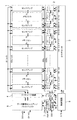
図15は、従来のDRAMのレプリカ回路を含む回路構成を示す。これは、各々1つのトランジスタと1つのキャパシタとで構成されたメモリセルMCと、ワード線WL0,WL1と、ビット線対BL0〜BLn/XBL0〜XBLnと、当該ビット線対BL0〜BLn/XBL0〜XBLnのデータを増幅するセンスアンプSA0〜SAnと、ダミーメモリセルDMCと、ダミーワード線DWLと、ダミービット線対DBL/XDBLと、当該ダミービット線対DBL、XDBLのデータを検出して信号を発生するデータ検出回路201と、センスアンプSA0〜SAnを起動するためのSA制御発生回路202とを備えたものである(例えば、特許文献1参照)。
FIG. 15 shows a circuit configuration including a conventional DRAM replica circuit. This is because the memory cells MC each composed of one transistor and one capacitor, the word lines WL0 and WL1, the bit line pairs BL0 to BLn / XBL0 to XBLn, and the bit line pairs BL0 to BLn / XBL0. Sense amplifiers SA0 to SAn that amplify data of XBLn, dummy memory cells DMC, dummy word lines DWL, dummy bit line pairs DBL / XDBL, and data of the dummy bit line pairs DBL and XDBL are detected and signals are output. A generated
図16のタイミングチャートを用いて、以上のように構成された従来の半導体記憶装置のコア動作に関して説明する。まずDRAMにアクセス要求があると、選択ワード線WL0が活性化されてメモリセルからの電荷がビット線BL0〜BLnに転送される。このとき同時にダミーワード線DWLも活性化されるため、ダミービット線DBLにも同様に電荷が転送される。この電荷転送動作によるダミービット線DBLの電位レベルの変動がデータ検出回路201の閾値を越えることによって、SA制御発生回路202が活性化され、SA制御信号SENが発生される。この信号によってセンスアンプSAが起動し、ビット線対BL/XBLを所望の電位まで増幅することができる。
The core operation of the conventional semiconductor memory device configured as described above will be described with reference to the timing chart of FIG. First, when there is an access request to the DRAM, the selected word line WL0 is activated and charges from the memory cells are transferred to the bit lines BL0 to BLn. At this time, the dummy word line DWL is also activated, so that charges are similarly transferred to the dummy bit line DBL. When the potential level fluctuation of the dummy bit line DBL due to the charge transfer operation exceeds the threshold value of the
このようにビット線データの増幅までのタイミングを、ダミーメモリセルを使って論理的に決定することによって、回路の誤動作をなくし、またタイミングの最適化を実現できるためタイミング動作を高速化できる。
しかしながら、従来の構成によれば、電荷によるレベル検出では、電位変化分が閾値を超えない場合に正しい回路動作ができないといった課題があった。特にメモリセルのように微少容量では、プロセスばらつきやリーク電流などの影響によってその課題は無視できない。 However, according to the conventional configuration, there is a problem that the level detection based on electric charges cannot perform a correct circuit operation when the potential change does not exceed the threshold value. In particular, in the case of a very small capacity such as a memory cell, the problem cannot be ignored due to the influence of process variations and leakage current.
また、設定した閾値が例えばトランジスタの閾値を使うような場合は、通常メモリセルからビット線に現れる電位変化と比べると非常に大きな電位となり、例えばダミーメモリセルの電荷量やビット線の寄生容量の削減などで通常のメモリセルアレイと大きく異なるレイアウト構成にする必要がでてくる。これではレプリカ回路として、センスアンプ起動の正確なタイミングを作ることが困難になってくる課題があった。 Further, when the set threshold value uses, for example, a transistor threshold value, the potential becomes very large compared to the potential change that appears on the bit line from the normal memory cell. For example, the charge amount of the dummy memory cell and the parasitic capacitance of the bit line Due to the reduction or the like, it is necessary to have a layout configuration greatly different from that of a normal memory cell array. This causes a problem that it becomes difficult for the replica circuit to make an accurate timing for starting the sense amplifier.
また、リファレンス電位などを使って微細電位差を読み出すような場合は、プロセスばらつきや外部条件に対応できるようなリファレンス電位を発生する回路の設計を実現しないといけないといった課題や、リファレンス回路を配置するための面積オーバーヘッドなどといった課題があった。 In addition, when reading out a fine potential difference using a reference potential or the like, there is a problem that the design of a circuit that generates a reference potential that can cope with process variations and external conditions must be realized, and in order to arrange the reference circuit There were problems such as area overhead.
また、DRAMのような、1)電荷読み出し動作、2)センス、リストア動作、3)プリチャージ動作の3つのメモリセル動作が必要な回路構成において、電荷読み出し動作のみのタイミングを高速化してもメモリセル全体の動作の高速化にもアクセス時間の高速化にも大きな効果を与えないといった課題があった。 Further, in a circuit configuration that requires three memory cell operations such as 1) charge read operation, 2) sense and restore operation, and 3) precharge operation, such as DRAM, even if the timing of only the charge read operation is increased, the memory There has been a problem that neither the speeding up of the operation of the entire cell nor the speeding up of the access time has a significant effect.
また、例えばスタティックランダムアクセスメモリ(SRAM)のようにビット線に電流を転送することでデータを読み出す回路構成とは異なり、DRAMのようなキャパシタにてデータを電荷で蓄積するメモリにおいて、メモリセル容量とビット線の寄生容量との容量比とセンスアンプ感度とによって1つのビット線につながるメモリセル数が制限されるため、ビット線につながるメモリセル数つまりワード線の本数を自由に変えることによるメモリ容量のラインナップ展開(例えば、ワード線数16〜512本で、ビット線数512本の場合、メモリ容量8Kビット〜256Kビットのバリエーション展開ができる)においても、レプリカ回路を使ってメモリ容量に応じた最適なセンスアンプ起動タイミングを生成することと、レプリカ回路の面積オーバーヘッドとのトレードオフではそれほど大きな効果は望めないといった課題があった。 In addition, unlike a circuit configuration in which data is read by transferring current to a bit line, such as a static random access memory (SRAM), a memory cell capacity in a memory such as a DRAM that stores data with electric charge. Since the number of memory cells connected to one bit line is limited by the capacitance ratio between the parasitic capacitance of the bit line and the sense amplifier sensitivity, the memory by freely changing the number of memory cells connected to the bit line, that is, the number of word lines Even in the lineup of capacitors (for example, when the number of word lines is 16 to 512 and the number of bit lines is 512, variations of the memory capacity of 8 Kbit to 256 Kbit can be developed), the replica circuit is used according to the memory capacity. Generate optimal sense amplifier start timing and replica Is a trade-off between road area overhead had a problem not expect a large effect so.
更に、混載メモリ、特に混載DRAMのようにメモリ容量が大きくて、かつ様々な仕様展開が必要な場合には、メモリ容量によってもビット線につながるメモリセル数を変えることよりも、ビット線につながるメモリセル数を変えずにビット線を含むメモリアレイ数を変えることで実現することの方が、回路動作の安定性でも回路面積の縮小においても効果的であるため、ビット線を増幅するセンスアンプの起動タイミングを論理的に決めるより、メモリ容量に応じて配線長や負荷が大きく変わるデータ線を増幅するセンスアンプの起動タイミングを論理的に決めることが高速化するための課題であっただけでなく、様々なメモリ仕様を容易に実現する上で重要であった。 Further, when the memory capacity is large and various specifications need to be developed as in the case of the embedded memory, especially the embedded DRAM, it is connected to the bit line rather than changing the number of memory cells connected to the bit line depending on the memory capacity. A sense amplifier that amplifies the bit line is realized by changing the number of memory arrays including bit lines without changing the number of memory cells, because it is more effective in terms of stability of circuit operation and reduction in circuit area. Rather than logically determining the start timing of the amplifier, the logical decision of the start timing of the sense amplifier that amplifies the data line that greatly changes the wiring length and load according to the memory capacity is only a problem for speeding up. However, it was important for easily realizing various memory specifications.
本発明は、上記問題を解決するものであって、メモリ容量に応じて変わり、かつデータアクセス時間上最も負荷が重いデータ線を増幅するセンスアンプの起動タイミングを論理的に決めることで高速なアクセス時間を実現でき、かつ様々なメモリ仕様を容易に実現できる半導体記憶装置を提供することを目的とする。 The present invention solves the above-mentioned problem, and changes the speed according to the memory capacity, and the access timing of the sense amplifier that amplifies the data line that amplifies the data load that is the heaviest in the data access time is logically determined. An object of the present invention is to provide a semiconductor memory device that can realize time and can easily realize various memory specifications.
この課題を解決するために、本発明の半導体記憶装置は、メモリセルと、メモリセルにつながるワード線及びビット線と、ビット線につながる第1のセンスアンプと、ダミーメモリセルと、ダミーメモリセルにつながるダミービット線と、ダミービット線につながる第2のセンスアンプと、第1のセンスアンプにつながるデータ線と、データ線につながる第3のセンスアンプと、第2のセンスアンプにつながるダミーデータ線と、ダミーデータ線につながる論理回路とを備えた半導体記憶装置であって、論理回路の出力信号が第3のセンスアンプを起動する入力信号であることを特徴とする。 In order to solve this problem, a semiconductor memory device of the present invention includes a memory cell, a word line and a bit line connected to the memory cell, a first sense amplifier connected to the bit line, a dummy memory cell, and a dummy memory cell. A dummy bit line connected to the second sense amplifier, a second sense amplifier connected to the dummy bit line, a data line connected to the first sense amplifier, a third sense amplifier connected to the data line, and a dummy data connected to the second sense amplifier. And a logic circuit connected to a dummy data line, wherein an output signal of the logic circuit is an input signal for starting a third sense amplifier.
更に、前記論理回路は、ダミービット線に読み出されたダイナミックデータを増幅する第2のセンスアンプで生成されたスタティックデータがダミーデータ線上の電位でトランジスタのスイッチング電位を超えたことを検知して出力される信号を、第3のセンスアンプを起動する入力信号とすることを特徴とする。 Further, the logic circuit detects that the static data generated by the second sense amplifier that amplifies the dynamic data read out to the dummy bit line exceeds the switching potential of the transistor at the potential on the dummy data line. The output signal is an input signal for starting the third sense amplifier.
このように、第2のセンスアンプで増幅されてかつ転送されたダミーデータ線上の電位レベルを使ってデータ線を増幅するための第3のセンスアンプのタイミングを生成するレプリカ回路構成によって、メモリ容量毎に負荷が大きく変わるデータ線の最適な転送タイミングを生成することができる。 As described above, the replica circuit configuration for generating the timing of the third sense amplifier for amplifying the data line using the potential level on the dummy data line amplified and transferred by the second sense amplifier allows the memory capacity to be increased. It is possible to generate the optimum transfer timing of the data line whose load greatly changes every time.
また、第2のセンスアンプを使ってダミーデータ線に電流を流し論理回路で検知する構成では、検知回路の閾値を超えないといった回路動作不具合やダミー回路部分のレイアウト構成が大きく変わることもないため、プロセスばらつきや外部条件に左右されない。 Further, in the configuration in which the current is passed through the dummy data line using the second sense amplifier and the logic circuit detects, the circuit operation failure such that the threshold value of the detection circuit is not exceeded and the layout configuration of the dummy circuit portion do not change significantly. Independent of process variations and external conditions.
また、ダミーメモリセルにつながるワード線と、メモリセルにつながるワード線とが同一配線であることで、レプリカ回路面積のオーバーヘッドをなくすとともに、アクセスされたメモリセルと物理的に近い場所からの起動でタイミングを作るためにタイミング誤差を小さくすることができる。 In addition, since the word line connected to the dummy memory cell and the word line connected to the memory cell are the same wiring, the overhead of the replica circuit area is eliminated, and startup from a location physically close to the accessed memory cell is possible. Timing errors can be reduced to create timing.
また、ダミーメモリセルがワードドライバを含むロウデコーダと隣り合って配置され、論理回路の出力タイミングを調節する遅延回路を有することにより、一番早く第3のセンスアンプの起動タイミングを生成することでアクセス時間の高速化を実現できるとともに、遅延回路によって第3のセンスアンプの起動タイミングを微調整できるために、タイミングが早すぎるための誤動作を防ぐことができる。 In addition, the dummy memory cell is arranged adjacent to the row decoder including the word driver, and has a delay circuit that adjusts the output timing of the logic circuit, so that the start timing of the third sense amplifier can be generated earliest. The access time can be increased, and the activation timing of the third sense amplifier can be finely adjusted by the delay circuit, so that a malfunction due to too early timing can be prevented.
また、ダミーデータ線に第2のセンスアンプがスイッチによって2つ以上つながる構成によって、論理回路の閾値レベルと第3のセンスアンプの閾値レベルが例えば4:1の場合、第2のセンスアンプを4個つなぐことで、第3のセンスアンプの最適な起動タイミングを実現できる。 Further, when two or more second sense amplifiers are connected to the dummy data line by a switch, when the threshold level of the logic circuit and the threshold level of the third sense amplifier are, for example, 4: 1, the second sense amplifier is set to 4 By connecting them individually, it is possible to realize the optimum activation timing of the third sense amplifier.
また、2本以上のダミーデータ線の論理和をとる機能を備えた論理回路を備え、2本以上のダミーデータ線のデータが同じ論理値であることを特徴とする。このように、ダミーデータの論理和によって第3のセンスアンプの起動タイミングを発生することで、1つのダミーデータ線に誤った信号が転送されても第3のセンスアンプの起動タイミング信号が発生しないということがなくすことができる。 In addition, a logic circuit having a function of taking a logical sum of two or more dummy data lines is provided, and data of two or more dummy data lines have the same logic value. As described above, the start timing of the third sense amplifier is generated by the logical sum of the dummy data, so that the start timing signal of the third sense amplifier is not generated even if an erroneous signal is transferred to one dummy data line. That can be eliminated.
更に、冗長構成の採用により、ワード線、それにつながるメモリセル又はダミーメモリセルに不良があった場合、冗長ワード線に置き換えることによってメモリを救済することができる。 Furthermore, by adopting a redundant configuration, when a word line, a memory cell connected to the word line, or a dummy memory cell is defective, the memory can be relieved by replacing it with a redundant word line.
また、ダミーメモリセルのデータを外部に読み出す手段を備えることで、データ線用のレプリカ回路が不良かどうかの判定をすることができる。 Further, by providing means for reading out data of the dummy memory cell to the outside, it is possible to determine whether or not the data line replica circuit is defective.
以上のように、本発明によれば、メモリ容量に応じて変わり、かつデータアクセス時間上最も負荷が重いデータ線を増幅するセンスアンプの起動タイミングを論理的に決めることで高速なアクセス時間を実現でき、かつ様々なメモリ仕様を容易に実現できる半導体記憶装置を提供することができる。 As described above, according to the present invention, a high-speed access time is realized by logically determining the start timing of the sense amplifier that amplifies the data line that varies depending on the memory capacity and has the heaviest load on the data access time. It is possible to provide a semiconductor memory device that can easily realize various memory specifications.
本発明の実施の最良の形態について、図面を参照しながら説明する。 The best mode for carrying out the present invention will be described with reference to the drawings.
《第1の実施の形態》
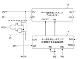
図1は、本発明の第1の実施の形態における半導体記憶装置の主要構成を示すブロック図である。図1において、1は1つのトランジスタと1つのキャパシタとで構成されたメモリセルと、当該メモリセルにつながるワード線及びビット線と、当該ビット線につながるセンスアンプとを含むメモリアレイ、2は1つのトランジスタと1つのキャパシタとで構成されたダミーメモリセル(前記メモリセルを構成する1つのトランジスタと1つのキャパシタと同じ回路構成であっても、また前記メモリセルとは違う回路構成であってもよい。)と、当該ダミーメモリセルにつながるワード線及びダミービット線と、当該ダミービット線につながるセンスアンプとを含むダミーメモリアレイ、3はメモリセル及びダミーメモリセルにつながるワード線を選択し活性化するためのロウデコーダ、4はメモリアレイ1にデータアクセスするためのデータ線対DL<m:0>/XDL<m:0>をプリチャージするためのプリチャージ回路、5はダミーメモリアレイ2にデータアクセスするためのダミーデータ線対DDL/XDDLをプリチャージするためのプリチャージ回路、6はデータ線対DL<m:0>/XDL<m:0>にデータを書き込む場合のライトバッファとデータを読み出す場合に増幅するためのデータ線用センスアンプとを含む回路ブロック(データ線用センスアンプ/ライトバッファ)、7はダミーデータ線DDLの電位がある閾値を超えるとデータ線用センスアンプ6を活性化するための信号を生成するデータ線用センスアンプ制御信号生成論理回路、8はメモリ動作をコントロールするための制御回路である。
<< First Embodiment >>
FIG. 1 is a block diagram showing the main configuration of the semiconductor memory device according to the first embodiment of the present invention. In FIG. 1, 1 is a memory array including a memory cell composed of one transistor and one capacitor, a word line and a bit line connected to the memory cell, and a sense amplifier connected to the bit line. A dummy memory cell composed of one transistor and one capacitor (even if the circuit configuration is the same as that of one transistor and one capacitor constituting the memory cell, or different from the memory cell) And a dummy memory array including a word line and a dummy bit line connected to the dummy memory cell and a sense amplifier connected to the dummy bit line, and 3 selects and activates a word line connected to the memory cell and the dummy memory cell. A row decoder 4 for data access, and data 4 for data access to the
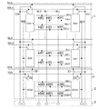
図2は、メモリアレイ1とダミーメモリアレイ2とロウデコーダ3との具体的な回路構成を示す。ここで、メモリアレイ1のビット線につながるメモリセル及びダミーメモリアレイ2のダミービット線につながるダミーメモリセルの数は、セル容量とビット線又はダミービット線の寄生容量との容量比と、センスアンプ感度及びメモリの要求速度とで決められた個数になっている。
FIG. 2 shows a specific circuit configuration of the
図3は、データ線用センスアンプ/ライトバッファ6の具体的な回路構成を示す。図3において、61はデータ線用センスアンプ、62はライトバッファである。
FIG. 3 shows a specific circuit configuration of the data line sense amplifier / write
図4は、データ線用センスアンプ制御信号生成論理回路7を示す。図4において、71はNOR回路、72はダミー用のライトバッファである。
FIG. 4 shows the data line sense amplifier control signal
図5のタイミングチャートを用いて、以上のように構成された半導体記憶装置のダミーメモリセルのレプリカ回路動作について説明する。まずメモリに読み出し要求があると、制御回路8でリード動作基準信号REAが生成されることで入力アドレス信号をロウデコーダ3に伝達し、デコード信号によって選択ワード線WL0が活性化される。これによってメモリセルMCからビット線BLにデータが転送される。同時にダミーメモリセルDMCからダミービット線DBLにLデータが転送される。これによって電源電圧VDD(又はHレベル)の1/2にプリチャージされたダミービット線DBLの電位がLレベル方向にダミービット線BLの寄生容量とダミーメモリセルDMCのセル容量比分だけ上昇する。同時に、周辺回路リード動作基準信号REも生成される。
The replica circuit operation of the dummy memory cell of the semiconductor memory device configured as described above will be described using the timing chart of FIG. First, when there is a read request in the memory, the
次に、メモリセルMC及びダミーメモリセルDMCからの電荷転送のための所定時間の遅延後、ビット線BL/XBL及びダミービット線DBL/XDBLにつながるセンスアンプSA0〜SAn及びDSA0,DSA1を活性化する信号SENがHレベルになり活性化される。これによって、ビット線BL/XBLはそれぞれH又はLレベルまで増幅される。同時にダミービット線DBLはLレベルまで増幅される。なお、センスアンプSA0〜SAnとDSA0,DSA1はプロセスパターンの均等化やビット線とダミービット線のセンス動作タイミングのばらつきをなくすために、同じ回路のセンスアンプを使用してもよい。また、センスアンプSA0〜SAnとDSA0,DSA1は違う回路構成のセンスアンプを使ってもよいことは言うまでもない。 Next, after a predetermined time delay for transferring charges from the memory cell MC and the dummy memory cell DMC, the sense amplifiers SA0 to SAn and DSA0 and DSA1 connected to the bit line BL / XBL and the dummy bit line DBL / XDBL are activated. The signal SEN to be activated becomes H level and activated. As a result, the bit lines BL / XBL are amplified to the H or L level, respectively. At the same time, the dummy bit line DBL is amplified to L level. The sense amplifiers SA0 to SAn and DSA0 and DSA1 may use sense amplifiers of the same circuit in order to equalize the process pattern and eliminate variations in the sense operation timing of the bit lines and the dummy bit lines. It goes without saying that sense amplifiers SA0 to SAn and DSA0 and DSA1 may use sense amplifiers having different circuit configurations.
次に、電源電圧VDDにプリチャージされたデータ線DL/XDLとダミーデータ線DDL/XDDLにビット線BL/XBLとダミービット線DBL/XDBLのデータを転送するためのカラムスイッチ信号CS0がHレベルになり活性化されることで、データ線DL/XDLにはそれぞれビット線BL/XBLからの所望のデータが、ダミーデータ線DDLにはダミービット線DBLのLレベルのデータが転送され、センスアンプDSA0によって増幅されたLレベルデータは、所定時間後にダミーデータ線DDLを1/2VDDレベルの電位にする。ダミーデータ線DDLは、データ線用センスアンプ制御信号生成論理回路7のNOR回路71の1つの入力につながっており、この入力信号につながるCMOSトランジスタのスイッチングレベルが1/2VDDである(すなわちCMOSトランジスタの出力論理が反転する)ことと、NOR回路71の他方の入力は周辺回路リード動作基準信号REのHレベル信号の反転信号となっていることから、データ線用センスアンプ制御信号生成論理回路7の出力信号DACNTがHレベルになりレプリカ回路動作が完了する。
Next, the column switch signal CS0 for transferring the data of the bit line BL / XBL and the dummy bit line DBL / XDBL to the data line DL / XDL and the dummy data line DDL / XDDL precharged to the power supply voltage VDD is at the H level. By being activated, the desired data from the bit line BL / XBL is transferred to the data line DL / XDL, and the L level data of the dummy bit line DBL is transferred to the dummy data line DDL, respectively. The L level data amplified by the
次に、信号DACNTがHレベルになることでデータ線用センスアンプ6が活性化され、データ線DL/XDLのデータを増幅することで、それぞれHレベル及びLレベルになる。増幅されたデータ線DLのデータがバッファ回路を通じて出力DOまで転送されることで読み出し動作が行われる。
Next, when the signal DACNT becomes H level, the data
最後に、リード動作基準信号REA及び周辺回路リード動作基準信号REが一定期間の後にLレベルになることで、メモリの内部回路が次の動作に備えるスタンバイ状態となる。 Finally, when the read operation reference signal REA and the peripheral circuit read operation reference signal RE become L level after a certain period, the internal circuit of the memory enters a standby state ready for the next operation.
以上のとおり、電荷転送により電位変化が閾値を超えなかった場合に二度と期待した動作ができなくなり、また負荷容量が固定されているビット線のデータを増幅するためのセンスアンプ起動タイミングには例えばトランジスタ遅延回路のような固定遅延時間を使用し、センスアンプを使って電流によってデータ転送を行うことで一定時間後には必ず所望の電位が得られ、また負荷容量がメモリ容量によって大きく変わるデータ線のデータを増幅するためのセンスアンプの起動タイミングは、メモリセル、ビット線、センスアンプ、カラムスイッチ、データ線までを同じ回路構成で実現したダミービット線、センスアンプ、カラムスイッチ、ダミーデータ線とNOR回路のような簡単なレベル検出回路によって構成されたレプリカ回路の出力信号を使うことで、例えば、メモリ容量が小さくなる場合、すなわちデータ線が短くなることで回路負荷が軽くなる場合は、ダミーデータ線が1/2VDDの電位になるまでの時間も短くなり、よってデータ線用センスアンプの起動が早くなるためにデータ出力つまりアクセス時間を高速にすることができる。また、例えば、メモリ容量が大きくなる場合、すなわちデータ線負荷が重くなる場合は、データ線を増幅するために所定の時間が長くなるために、プロセスばらつきや外部条件に影響を受けやすい遅延回路などを使ったタイミング発生回路より安定的かつ高速なデータ線センスアンプ起動を実現できる有効な手段である。 As described above, when the potential change does not exceed the threshold due to charge transfer, the expected operation cannot be performed again, and the sense amplifier activation timing for amplifying the data of the bit line with the fixed load capacitance is, for example, a transistor By using a fixed delay time such as a delay circuit and performing data transfer with current using a sense amplifier, a desired potential can always be obtained after a certain time, and the data of the data line whose load capacity varies greatly depending on the memory capacity The sense amplifier start-up timing for amplifying the data is a dummy bit line, sense amplifier, column switch, dummy data line and NOR circuit, which are realized with the same circuit configuration from the memory cell, bit line, sense amplifier, column switch, and data line. The output of a replica circuit configured by a simple level detection circuit such as For example, when the memory capacity is reduced, that is, when the circuit load is reduced by shortening the data line, the time until the dummy data line becomes a potential of 1/2 VDD is shortened. Since the activation of the data line sense amplifier is accelerated, the data output, that is, the access time can be increased. Further, for example, when the memory capacity is increased, that is, when the data line load is heavy, a predetermined time is increased to amplify the data line, so that the delay circuit is easily affected by process variations and external conditions. This is an effective means that can realize a data line sense amplifier start-up that is more stable and faster than the timing generation circuit using the.
なお、図4でNOR回路71を使用しているが、CMOSトランジスタのスイッチング機能など簡単な回路動作によって実現できる回路構成であればよいことは言うまでもない。また、それとは別にダミーデータ線にデータ線用センスアンプ61と同じ負荷トランジスタを付けた構成を負荷することはタイミングの最適化の意味で重要である。
Although the NOR
また、メモリセル及びダミーメモリセルを1つのトランジスタと1つのキャパシタ構成にすることで、蓄積されたデータがダイナミックデータの時の高速化には有効な手段となるが、メモリセルにダイナミックデータが蓄積される構成であるならばよく、例えば2つのトランジスタと2つのキャパシタ構成などであってもよい。 In addition, the memory cell and the dummy memory cell having one transistor and one capacitor structure are effective means for increasing the speed when the stored data is dynamic data. However, the dynamic data is stored in the memory cell. For example, two transistors and two capacitors may be used.
また、メモリセルとダミーメモリセルにつながるワード線を共通にすることで、改めてレプリカ回路用にダミーワード線を構成する必要がないために回路面積を削減できるとともに、同じワード線のためにメモリセルとダミーメモリセルのアクセストランジスタのゲートを同じタイミングで活性化できるために、ビット線及びダミービット線にデータが転送されるタイミングを同じタイミングにすることができる。すなわち、レプリカ回路の動作タイミングとしては最適なタイミングとなる。また、キャパシタセルに必要なリフレッシュ動作も、同一ワード線につながっているためにメモリセルをリフレッシュすると同時にダミーメモリセルもリフレッシュできるために、ダミーメモリセルのみ特別なリフレッシュ動作を必要としないため有効な手段である。なお、メモリセルとダミーメモリセルが異なるワード線につながる構成であってもよいことは言うまでもない。 In addition, since the word line connected to the memory cell and the dummy memory cell is made common, it is not necessary to form a dummy word line for the replica circuit, so that the circuit area can be reduced and the memory cell for the same word line can be reduced. Since the gates of the access transistors of the dummy memory cell can be activated at the same timing, the timing at which data is transferred to the bit line and the dummy bit line can be made the same timing. That is, the operation timing of the replica circuit is optimal. Also, the refresh operation required for the capacitor cell is effective because it is connected to the same word line, so that the dummy memory cell can be refreshed at the same time as the memory cell is refreshed, so that only the dummy memory cell does not require a special refresh operation. Means. Needless to say, the memory cell and the dummy memory cell may be connected to different word lines.
また、ビット線及びダミービット線と、データ線とダミーデータ線とがそれぞれ平行に配置されていることで、ビット線及びダミービット線と、データ線とダミーデータ線とが垂直に配置された場合と比較すると、ダミーデータ線の負荷とデータ線の負荷が等しくできるため、ダミーデータ線を含むレプリカ回路によるタイミング生成がデータ線の増幅タイミングを最適化できるため有効である。なお、本明細書ではビット線とデータ線の関係について言及しているが、スタティックデータになった後のレプリカ回路構成であるならば、ビット線と直接スイッチを介してつながるデータ線でも、そのデータ線とスイッチを介してつながるデータ線におけるレプリカ回路構成であってもよいのは言うまでもない。 In addition, when the bit line, the dummy bit line, the data line, and the dummy data line are arranged in parallel, the bit line, the dummy bit line, the data line, and the dummy data line are arranged vertically. As compared with, the load of the dummy data line and the load of the data line can be made equal, so that the timing generation by the replica circuit including the dummy data line is effective because the amplification timing of the data line can be optimized. In this specification, reference is made to the relationship between the bit line and the data line. However, if the replica circuit configuration has been changed to static data, even if the data line is connected directly to the bit line via a switch, the data It goes without saying that a replica circuit configuration in a data line connected to the line via a switch may be used.
また、図1のようにダミーメモリアレイ2がロウデコーダ3と隣り合って配置されると、データ線用センスアンプ制御信号生成論理回路7の出力信号DACNTの出力タイミングを調整する遅延回路を備えることで、ダミーメモリセルがそれ以外の場所、例えばロウデコーダ3から一番離れた場所にある場合と比較すると、回路の動作タイミングとしては一番早い動作となるためにデータ出力までのタイミングを最も早くできるためにメモリの高速化に有効である。また、出力タイミングが早すぎた場合の誤動作防止対策として、タイミングの微調節用の遅延回路を配置することは有効な手段である。なお、この遅延回路の調節はフューズや不揮発メモリなどを使って行う手段が有効なのは、マスク変更などが要らないことなどからも有効な手段であることは言うまでもない。
Further, when the
また、ダミーメモリセルの隣り合うキャパシタが接合していることでビット線への読み出し電荷量が増えるために安定したセンスアンプ動作を実現することができるため、レプリカ回路の動作保証としては有効である。なお、ダミーメモリセルがメモリセルより大きなキャパシタをもつ構成であればよいのは言うまでもなく、キャパシタの電極のショートで実現する場合でも、新たなキャパシタを構成してもよい。 In addition, since the adjacent capacitor of the dummy memory cell is joined to increase the amount of charge read to the bit line, a stable sense amplifier operation can be realized, which is effective as guaranteeing the operation of the replica circuit. . Needless to say, the dummy memory cell may have a larger capacitor than the memory cell, and a new capacitor may be formed even when the dummy memory cell is realized by short-circuiting the electrode of the capacitor.
また、図1のようにメモリアレイ1とダミーメモリアレイ2とを同数だけ配置することで、選択されたワード線の物理的にそれぞれのアレイがある位置に合わせた場所からレプリカ回路を起動できるため、最適なタイミングを発生できる有効な手段である。また、ワード線をメモリアレイ1とダミーメモリアレイ2とで共通に接続することで、選択されたワード線からダミーメモリセル及びメモリセルデータが読み出されるために、より最適なタイミングを生成できる。また、ダミーメモリアレイ2を例えば1箇所だけ配置するような構成にすればタイミングの最適化に障害が出るだけでなく、メモリセルのパターン不均衡によるプロセス不具合や、ダミーメモリアレイがない場所がデッドスペース化することによる面積オーバーヘッドの課題を解決する手段でもある。
In addition, since the same number of
また、ダミーメモリセルが1つのトランジスタで構成され、トランジスタのソースノードが電源につながっていることによって、ダミーメモリセルキャパシタの欠陥に対して考慮する必要がなくなり、またダミーメモリセルへ読み出しに必要なデータを書き込む必要がないために有効な手段である。なお、ダミーメモリセルとして1つのトランジスタで構成するとしているが、2つ以上のトランジスタで構成してもよいことは言うまでもない。 Further, since the dummy memory cell is composed of one transistor and the source node of the transistor is connected to the power supply, it is not necessary to consider the defect of the dummy memory cell capacitor, and it is necessary for reading to the dummy memory cell. This is an effective means because it is not necessary to write data. Although the dummy memory cell is composed of one transistor, it is needless to say that it may be composed of two or more transistors.
また、図6で示す通り、論理回路7の出力にラッチ回路73を備えることで、ダミーセンスアンプにつながるカラムスイッチがオフしても、周辺回路リード動作基準信号REがHの期間中は出力データをラッチできるため、有効な手段である。
Further, as shown in FIG. 6, by providing the
次に図7を用いて、ダミーデータ線にセンスアンプがスイッチによって2つ以上つながる構成について説明する。図7が示すように、ダミーデータ線DDL/XDDLにセンスアンプDSA0及びDSA1の2つが、各々制御信号DCSによりゲートが制御されるNチャンネルトランジスタ20,21;22,23を介してつながる構成になっている。これによって、メモリセルのデータ線DL/XDLよりダミーメモリセルのダミーデータ線DDL/XDDLの方が2倍の速度でデータを読み出すことができるため、データ線用センスアンプ6にてデータ線DL/XDLを増幅するために必要な電位差とデータ線用センスアンプ制御信号生成論理回路7のNOR回路71のスイッチングするために必要な電位差とが1:2の場合、レプリカ回路のデータ線用センスアンプ起動信号の生成タイミングとデータ線用センスアンプ61の増幅するためのタイミングとを等価にすることができるため有効な手段である。
Next, a configuration in which two or more sense amplifiers are connected to the dummy data line by a switch will be described with reference to FIG. As shown in FIG. 7, two sense amplifiers DSA0 and DSA1 are connected to dummy data lines DDL / XDDL via N-
また、センスアンプのカラムスイッチの制御信号とダミーセンスアンプのカラムスイッチの制御信号とが異なる構成にすることで、ダミーセンスアンプのカラムスイッチがカラムデコード入力に関係なく制御できるため容易に複数のダミーセンスアンプを1つのダミーデータ線に接続することができる。また、ダミーセンスアンプの数が変わってもセンスアンプのカラムスイッチの駆動タイミングや駆動能力に影響を及ぼさないため有効である。 Also, by configuring the sense amplifier column switch control signal and the dummy sense amplifier column switch control signal to be different, the dummy sense amplifier column switch can be controlled regardless of the column decode input. The sense amplifier can be connected to one dummy data line. Further, even if the number of dummy sense amplifiers changes, it is effective because it does not affect the drive timing and drive capability of the column switch of the sense amplifier.
次に図8を用いて、ダミーデータ線が相補線ではなく、ダミーデータ線に隣接する配線が電源線である構成について説明する。図8が示すように、ダミーデータ線DDLはセンスアンプDSA0及びDSA1に、各々カラムスイッチ信号CS0及びCS1によりゲートが駆動されるNチャンネルトランジスタ20,21を介してつながっている。一方のセンスアンプDSA0及びDSA1につながるNチャンネルトランジスタ22,23は、ゲートをVSS電源、ソースをオープンにしている。この構成によって、ダミーデータ線の相補の一方がVSS電源線のため、レプリカ回路動作に必要なダミーデータ線の読み出し動作に対してシールド効果として使用できるだけでなく、負荷の重いダミーデータ線の動作を1本だけにすることによる消費電流の削減効果が期待できる。なお、VSS電源線としているが、VDD電源線としてもよいことは言うまでもなく、その場合、Nチャンネルトランジスタのソースノードに接続し、ゲートノードをVSS電源につなぐなどといった手段がある。
Next, a configuration in which the dummy data line is not a complementary line and the wiring adjacent to the dummy data line is a power supply line will be described with reference to FIG. As shown in FIG. 8, the dummy data line DDL is connected to the sense amplifiers DSA0 and DSA1 through N-
なお、以上の形態はそれぞれを組み合わせることで、より一層の効果を期待できることは言うまでもない。 In addition, it cannot be overemphasized that the further effect can be anticipated by combining each of the above forms.
《第1の実施の形態の変形例》
図9は、本発明の第1の実施の形態の変形例における半導体記憶装置の主要構成を示すブロック図である。特に、データ線用センスアンプ制御信号生成論理回路9が第1の実施の形態と異なり、具体的な回路図としては図10に示すとおりである。図10において、91はNOR回路群、92はダミー用のライトバッファ群、93はOR回路であり、複数本のダミーデータ線DDL<0>〜DDL<n>の論理和をデータ線用センスアンプ6の制御信号DACNTとしている。
<< Modification of First Embodiment >>
FIG. 9 is a block diagram showing a main configuration of the semiconductor memory device according to the modification of the first embodiment of the present invention. In particular, the data line sense amplifier control signal
当該変形例によれば、複数のダミーデータ線の論理和をとることで、ダミーメモリセルの1つに不良があった場合でも、残りのダミーデータ線からのデータをデータ線用センスアンプ制御信号生成論理回路9に転送できるため、所望のレプリカ回路の動作を実現できる有効な手段である。通常、このダミーデータ線数はプロセス上の欠陥の発生率と回路面積のオーバーヘッドとのトレードオフで決めることができる。また、2本以上のダミーデータ線のデータは全て同じ論理値であることは言うまでもない。
According to the modification, by taking a logical sum of a plurality of dummy data lines, even if there is a defect in one of the dummy memory cells, the data from the remaining dummy data lines is used as a data line sense amplifier control signal. Since it can be transferred to the
なお、本実施の形態と第1の実施の形態を組み合わせることで、より一層の効果を期待できることは言うまでもない。 Needless to say, a further effect can be expected by combining the present embodiment and the first embodiment.
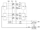
《第2の実施の形態》
図11は、本発明の第2の実施の形態における半導体記憶装置の主要構成を示すブロック図である。図11において、10、11はそれぞれ冗長ワード線RWL0を含むメモリアレイ、ダミーメモリアレイ、12はメモリアレイ10及びダミーメモリアレイ11に欠陥があった場合に冗長ワード線へ切り替えることができる冗長デコード回路を含むロウデコーダである。
<< Second Embodiment >>
FIG. 11 is a block diagram showing a main configuration of the semiconductor memory device according to the second embodiment of the present invention. In FIG. 11, 10 and 11 are a memory array including a redundant word line RWL0, a dummy memory array, and 12 is a redundant decoding circuit capable of switching to a redundant word line when the
以上のように構成された半導体記憶装置にて、メモリアレイ10のWL0につながるメモリセルに欠陥があった場合、例えばフューズ機能などを使って冗長するワード線のアドレスを指定し、もしアクセスが欠陥ワード線WL0にヒットした場合、冗長デコード回路によって、冗長ワード線RWL0にアクセスを切り替えるような制御を行い、冗長メモリセルからビット線BLにデータを転送する。これによって欠陥セルの救済が可能となる。
In the semiconductor memory device configured as described above, when a memory cell connected to WL0 of the
同様に、ダミーメモリアレイ11のWL0につながるダミーメモリセルに欠陥があった場合も、冗長デコード回路によって冗長ワード線RWL0にアクセスを切り替えるような制御をできるため、ダミーメモリアレイ11の救済も可能となる。
Similarly, even when a dummy memory cell connected to WL0 of the
このように、従来存在していた冗長メモリセル及び冗長ワード線のような冗長回路をダミーメモリアレイにも適用することで、ダミーメモリアレイの欠陥救済までできるためにレプリカ回路の安定的な実現が可能になるだけでなく、冗長メモリセルを置くことによるダミーメモリアレイ内のデッドスペースを有効利用できるため有効な手段である。 In this way, by applying redundant circuits such as redundant memory cells and redundant word lines, which have existed in the past, to the dummy memory array, it is possible to relieve the defects of the dummy memory array, so that the replica circuit can be stably realized. This is not only possible, but it is an effective means because the dead space in the dummy memory array by placing redundant memory cells can be used effectively.
なお、本実施の形態と第1の実施の形態及び第1の実施の変形例を組み合わせることで、より一層の効果を期待できることは言うまでもない。 It goes without saying that a further effect can be expected by combining this embodiment with the first embodiment and the modification of the first embodiment.
《第3の実施の形態》
次に、本発明の第3の実施の形態について説明する。本実施の形態における半導体記憶装置の主要構成は図1〜図4のとおりであり、ダミーメモリアレイへのデータ書き込み動作に関して図12のタイミングチャートを用いて説明する。
<< Third Embodiment >>
Next, a third embodiment of the present invention will be described. The main configuration of the semiconductor memory device in the present embodiment is as shown in FIGS. 1 to 4, and the data write operation to the dummy memory array will be described with reference to the timing chart of FIG.
まずメモリに書き込み要求があると、制御回路8でライト動作基準信号WEAが生成され、周辺回路ライト動作基準信号WEが生成される。これによってデータ入力信号DIはライトバッファ6でドライブされ、データ線DL/XDLへデータを転送する。同時に、データ線用センスアンプ制御信号生成論理回路7のライトバッファ72によって、ダミーデータ入力信号DDIをダミーデータ線DDL/XDDLへデータを転送する。また、ライト動作基準信号WEAによって、入力アドレス信号はロウデコーダ3に伝達され、デコード信号によって選択ワード線WL0が活性化される。この後、選択ワード線WL0につながるメモリセル及びダミーメモリセルからビット線BL/XBL及びダミービット線DBL/XDBLに読み出されたデータはセンスアンプ活性化信号SENによって増幅される。次に、データ線とセンスアンプ及びダミーデータ線とセンスアンプをつなぐNチャンネルトランジスタのゲートを駆動するカラムスイッチ信号CS0が活性化されることで、データ線DL/XDLのデータがセンスアンプを介してメモリセルに書き込まれる。同様に、ダミーデータ線DDL/XDDLのデータもセンスアンプを介してダミーメモリセルに書き込まれる。
First, when there is a write request to the memory, the
最後に、ライト動作基準信号WEA及び周辺回路ライト動作基準信号WEが一定期間の後にLレベルになることで、メモリの内部回路が次の動作に備えるスタンバイ状態となる。 Finally, the write operation reference signal WEA and the peripheral circuit write operation reference signal WE are set to the L level after a certain period, so that the internal circuit of the memory enters a standby state for the next operation.
以上のとおり、書き込み要求時にメモリセルへ所望のデータを書き込むと同時に、ダミーメモリセルへも所望のデータを書き込む機能を備えることで、ダミーメモリセルからダミービット線、センスアンプ及びダミーデータ線のデータを所望のデータ値とすることができるため有効な手段である。また、ダミーメモリセルの初期化又は所望データの書き込みをメモリセルの書き込み時と同時に行うため、回路動作のオーバーヘッドをなくす有効な手段である。 As described above, the data of the dummy bit line, the sense amplifier, and the dummy data line is provided from the dummy memory cell by providing the function of writing the desired data to the memory cell at the same time as the write request at the time of the write request. Can be set to a desired data value, which is an effective means. In addition, since initialization of dummy memory cells or writing of desired data is performed simultaneously with the writing of memory cells, this is an effective means for eliminating the overhead of circuit operation.
また、ダミービット線DDL/XDDLにつながるライトバッファ72の入力信号DDIがVDD電源又は接地電位に接続されることによって、メモリへの新たな入力信号を追加することなく、書き込み要求に合わせて所望のアドレスにつながるダミーメモリセルへ固定データを書き込むことができるため、メモリのピン数削減の上でも有効である。
Further, the input signal DDI of the
また、ダミーデータ線DDL/XDDLにつながるライトバッファ72の入力信号DDIの論理値を外部から変更でき、かつ入力信号DDIの論理レベルを変えてもデータ線用センスアンプ制御信号発生論理回路7の出力信号DACNTの活性化時の論理レベルが変わらないように、図示していないが、例えば選択回路によってインバータ1段分異なる2つの信号経路を作って入力信号DDIの電位レベルによって切り替える機能を備えることによって、プロセス条件や外部条件などによってできるダミーメモリセルの読み出し動作の不均衡(例えば、Hレベルに比べてLレベルが読み出しやすいなど)を、例えば読み出しやすいデータ値に統一することで、ダミーメモリセルを含むレプリカ回路の安定動作を実現できる。
Further, the logic value of the input signal DDI of the
また、全てのワード線と全てのダミーメモリセルにつながるセンスアンプと全てのダミーメモリセルにつながるセンスアンプとダミーデータ線をつなぐスイッチを活性化する機能を備えることで、レプリカ回路動作のための所望のデータをダミーメモリセルへ一括して書き込めるため、例えばメモリの初期シーケンス時やスタンバイモードなどの空き時間に効率的に実行できる。また、この機能をモード設定機能とすることで、モード設定された一括書き込む動作時以外、例えばダミーデータ線へ書き込むためのライトバッファを止めるための制御を加えることで、メモリへの通常の書き込む要求時にはダミーデータ線を含むダミーメモリセルへの書き込み動作は制限されるため、消費電流を削減できる効果がある。また通常動作と同時に行う必要がないために、例えば動作周波数を十分遅くしてマージンをもってダミーメモリセルへの書き込み動作をすることで、レプリカ回路動作の安定動作を実現することができる。 In addition, it has a function of activating a switch connecting the sense amplifier connected to all the word lines and all the dummy memory cells and the sense amplifier connected to all the dummy memory cells and the dummy data line. Can be written into the dummy memory cells all at once, so that the data can be efficiently executed, for example, during an initial sequence of the memory or in idle time such as a standby mode. In addition, by setting this function as a mode setting function, a normal write request to the memory can be performed by adding control for stopping the write buffer for writing to the dummy data line, for example, other than during the mode setting batch writing operation. Since the write operation to the dummy memory cell including the dummy data line is sometimes limited, the current consumption can be reduced. Further, since it is not necessary to perform the operation at the same time as the normal operation, a stable operation of the replica circuit operation can be realized by, for example, performing a write operation to the dummy memory cell with a sufficiently low operating frequency and a margin.
なお、本実施の形態と前記各実施の形態を組み合わせることで、より一層の効果を期待できることは言うまでもない。 It goes without saying that a further effect can be expected by combining this embodiment and each of the above embodiments.
《第3の実施の形態の変形例》
図13は、本発明の第3の実施の形態の変形例における半導体記憶装置の主要構成を示すブロック図である。図13のように構成された半導体記憶装置のメモリアレイ101に付設されたダミーメモリアレイ102へのデータ書き込み動作に関して説明する。
<< Modification of Third Embodiment >>
FIG. 13 is a block diagram showing a main configuration of a semiconductor memory device according to a modification of the third embodiment of the present invention. A data write operation to the
外部からの制御信号CNTによってモードレジスタ111でダミーメモリアレイ102へのデータ書き込み動作を規定するフラグINTが活性化される。これによってライトバッファ110が活性化されることでダミーデータ入力信号DDIをダミーデータ線DDLへ転送する。選択回路112ではフラグINTがHデータのため、一定の周期でHレベルとLレベルを繰り返す入力信号DCLKが選択され、リフレッシュカウンタ113をカウントアップしていく。このリフレッシュカウンタ113のカウントアップ動作で選択されたアドレス信号はロウデコーダ103でデコードされて、リフレッシュ時と同様に全てのワード線を順次選択していく動作を行う。このワード線動作と同様に、選択ワード線につながるセンスアンプも活性化され、また図示していないがダミーメモリアレイ102につながるセンスアンプとダミーデータ線DDLをつなぐスイッチも選択されたセンスアンプにつながるスイッチのみ活性化されることで、ダミーメモリアレイ102へ所望のデータを書き込むことができる。この動作をリフレッシュカウンタ113が一周するまで続けることで全てのダミーメモリアレイ102へのデータ書き込みを完了できる。
A flag INT that defines a data write operation to the
また、通常のリフレッシュ要求に対しては、フラグINTが非活性状態のためリフレッシュコマンド信号REFを受けてリフレッシュカウンタ113が動作する構成になっている。
In response to a normal refresh request, the
以上のように、既存のメモリ回路を使って、ダミーメモリアレイ102への一括書き込み動作のような瞬間的に大電流を流す動作を必要とせず、かつ通常動作と異なるタイミングでダミーメモリアレイ102の初期化ができるとともに、メモリアレイ101とダミーメモリアレイ102とのリフレッシュ動作も同時に実現できるため、回路動作、消費電流、回路面積の上で最適な回路を実現できる。
As described above, using an existing memory circuit, an operation of passing a large current instantaneously as in a batch write operation to the
なお、一例としてモードレジスタ111を使ったモード設定によってダミーメモリアレイ102への書き込み動作を規定したが、リフレッシュカウンタ113を使ったダミーメモリアレイ102への書き込み動作を実現できる回路構成であるならばどのような回路構成でもよいことは言うまでもない。
As an example, the write operation to the
《第4の実施の形態》
図14は、本発明の第4の実施の形態における半導体記憶装置の主要構成を示すブロック図である。図14において、13は出力選択回路であり、テスト時の出力信号PDOは、メモリセルからのデータ出力DOのテスト出力と、データ線用センスアンプ制御信号生成論理回路7の出力信号DDOとをモード選択信号MODEで切り替えて出力できる回路構成になっている。
<< Fourth Embodiment >>
FIG. 14 is a block diagram showing a main configuration of a semiconductor memory device according to the fourth embodiment of the present invention. In FIG. 14,
以上のように構成された半導体記憶装置のダミーメモリセルのデータ読み出し動作について説明する。 A data read operation of the dummy memory cell of the semiconductor memory device configured as described above will be described.
図5で示すレプリカ回路動作で信号DACNTがHレベルになると、図4で示すようにデータ線用センスアンプ制御信号生成論理回路7のもう一方の出力信号DDOもHレベルとなる。このときモード選択信号MODEがHレベルであると、出力信号PDOにHレベルのデータが出力される。
When the signal DACNT becomes H level in the replica circuit operation shown in FIG. 5, the other output signal DDO of the data line sense amplifier control signal
また、モード選択信号MODEがLレベルの場合はメモリセルからの出力信号DOがテスト出力信号PDOに出力される。このようにデータ線用センスアンプ制御信号生成論理回路7の出力DDOの外部出力のON/OFFを切り替えることができる。
When the mode selection signal MODE is at L level, the output signal DO from the memory cell is output as the test output signal PDO. Thus, ON / OFF of the external output of the output DDO of the data line sense amplifier control signal
以上のように、メモリのテスト結果をモード選択することでダミーメモリセルのデータを外部に出力する手段を持つため、ダミーメモリセルを含むレプリカ回路の欠陥検査をすることができるため、メモリセルだけでなくダミーメモリセルにも不良箇所の特定、冗長救済といったメモリの救済処置を実施することができる。 As described above, since there is a means for outputting the data of the dummy memory cell to the outside by selecting the mode of the test result of the memory, the defect circuit of the replica circuit including the dummy memory cell can be inspected, so only the memory cell In addition, it is possible to carry out memory remedy treatment such as identification of a defective portion and redundancy remedy for a dummy memory cell.
なお、一例ではデータ線用センスアンプ制御信号生成論理回路7の出力DDOを選択信号を通してそのまま出力させているが、出力DDOをラッチする構成によって安定した外部出力結果を得る回路構成であってもよいのは言うまでもない。
In the example, the output DDO of the data line sense amplifier control signal
また、データ線用センスアンプ制御信号生成論理回路7の出力DDOが複数ある場合に、データ出力の一部又は全部の経路を使うことによって、テスト時に通常あったテスト出力端子を使って、ダミーメモリセルのデータ確認用に特別に出力端子を増やす必要なくダミーメモリセルからのデータを読み出すことができるため、メモリの端子数削減や回路面積削減において有効な手段である。
In addition, when there are a plurality of outputs DDO of the data line sense amplifier control signal
また、データ線及びダミーデータ線にそれぞれプリチャージ回路を備え、データ線のプリチャージ電位とダミーデータ線のプリチャージ電位とが異なるようにする。一例としてダミーデータ線のプリチャージ電位をVDD電位として、トランジスタのスイッチング特性を使ってデータ線を増幅するリードアンプの起動タイミングを生成し、データ線のプリチャージ電位は1/2VDD電位にすることで、メモリで多数あるデータ線で消費する電力を、VDDプリチャージ電位と比較して1/2に抑えることができるため、メモリの低消費電力化において有効な手段である。 Each of the data line and the dummy data line is provided with a precharge circuit so that the precharge potential of the data line is different from the precharge potential of the dummy data line. As an example, the precharge potential of the dummy data line is set to the VDD potential, the start timing of the read amplifier that amplifies the data line is generated using the switching characteristics of the transistor, and the precharge potential of the data line is set to 1/2 VDD potential. Since the power consumed by a large number of data lines in the memory can be suppressed to ½ compared to the VDD precharge potential, this is an effective means for reducing the power consumption of the memory.
なお、本実施の形態と前記各実施の形態を組み合わせることで、より一層の効果を期待できることは言うまでもない。 It goes without saying that a further effect can be expected by combining this embodiment and each of the above embodiments.
本発明に係る半導体記憶装置は、メモリ容量に応じて変わり、かつデータアクセス時間上最も負荷が重いデータ線を増幅するセンスアンプの起動タイミングを論理的に決めることで高速なアクセス時間を実現でき、かつ様々なメモリ仕様を容易に実現できる効果を有し、メモリを多数かつ多種類の仕様を搭載するシステムLSIなどに有用である。 The semiconductor memory device according to the present invention can realize a high-speed access time by logically determining the start timing of the sense amplifier that amplifies the data line that varies depending on the memory capacity and has the heaviest load on the data access time, In addition, it has an effect that various memory specifications can be easily realized, and is useful for a system LSI or the like in which a large number of memories and various types of specifications are mounted.
1 メモリアレイ
2 ダミーメモリアレイ
3 ロウデコーダ
4 プリチャージ回路
5 プリチャージ回路
6 データ線用センスアンプ/ライトバッファ
7 データ線用センスアンプ制御信号生成論理回路
8 制御回路
9 データ線用センスアンプ制御信号生成論理回路2
10 冗長セルを含むメモリアレイ
11 冗長セルを含むダミーメモリアレイ
12 冗長デコード回路を含むロウデコーダ
13 出力選択回路
20〜23 カラムスイッチを構成するNチャンネルトランジスタ
61 データ線用センスアンプ
62 ライトバッファ
71 NOR回路
72 ダミー用のライトバッファ
73 ラッチ回路
91 NOR回路群
92 ダミー用のライトバッファ群
93 OR回路
101 メモリアレイ
102 ダミーメモリアレイ
103 ロウデコーダ
110 ダミー用のライトバッファ
111 モードレジスタ
112 選択回路
113 リフレッシュカウンタ
201 データ検出回路
202 SA制御発生回路
DESCRIPTION OF
DESCRIPTION OF
Claims (26)
前記メモリセルにつながるワード線及びビット線と、
前記ビット線につながる第1のセンスアンプと、
ダミーメモリセルと、
前記ダミーメモリセルにつながるダミービット線と、
前記ダミービット線につながる第2のセンスアンプと、
前記第1のセンスアンプにつながるデータ線と、
前記データ線につながる第3のセンスアンプと、
前記第2のセンスアンプにつながるダミーデータ線と、
前記ダミーデータ線につながる論理回路とを備えた半導体記憶装置であって、
前記論理回路は、前記ダミービット線に読み出されたダイナミックデータを増幅する前記第2のセンスアンプで生成されたスタティックデータが前記ダミーデータ線上の電位でトランジスタのスイッチング電位を超えたことを検知して出力される信号を、前記第3のセンスアンプを起動する入力信号とすることを特徴とする半導体記憶装置。 A memory cell;
A word line and a bit line connected to the memory cell;
A first sense amplifier connected to the bit line;
A dummy memory cell;
A dummy bit line connected to the dummy memory cell;
A second sense amplifier connected to the dummy bit line;
A data line connected to the first sense amplifier;
A third sense amplifier connected to the data line;
A dummy data line connected to the second sense amplifier;
A semiconductor memory device comprising a logic circuit connected to the dummy data line,
The logic circuit detects that the static data generated by the second sense amplifier that amplifies the dynamic data read to the dummy bit line exceeds the switching potential of the transistor at the potential on the dummy data line. The semiconductor memory device is characterized in that the output signal is an input signal for starting the third sense amplifier .
前記論理回路の出力にラッチ回路を備えたことを特徴とする半導体記憶装置。 The semiconductor memory device according to claim 1.
A semiconductor memory device comprising a latch circuit at the output of the logic circuit.
前記論理回路の出力信号の論理値によって、前記論理回路の入力になるダミーデータ線の信号をラッチする手段を備えたことを特徴とする半導体記憶装置。 The semiconductor memory device according to claim 1.
A semiconductor memory device comprising means for latching a signal of a dummy data line that is input to the logic circuit according to a logic value of an output signal of the logic circuit.
前記メモリセル及びダミーメモリセルは、各々1つのトランジスタと1つのキャパシタとで構成されていることを特徴とする半導体記憶装置。 The semiconductor memory device according to claim 1.
Each of the memory cell and the dummy memory cell is composed of one transistor and one capacitor.
前記ダミーメモリセルにつながるワード線と、前記メモリセルにつながるワード線とが同一配線であることを特徴とする半導体記憶装置。 The semiconductor memory device according to claim 1.
A word line connected to the dummy memory cell and a word line connected to the memory cell are the same wiring.
前記ビット線及び前記ダミービット線と、前記データ線及び前記ダミーデータ線とがそれぞれ平行に配置されていることを特徴とする半導体記憶装置。 The semiconductor memory device according to claim 1.
The semiconductor memory device, wherein the bit line and the dummy bit line are arranged in parallel with the data line and the dummy data line.
前記ダミーメモリセルがワードドライバを含むロウデコーダと隣り合って配置され、前記論理回路の出力タイミングを調節する遅延回路を有することを特徴とする半導体記憶装置。 The semiconductor memory device according to claim 1.
A semiconductor memory device, wherein the dummy memory cell is disposed adjacent to a row decoder including a word driver, and has a delay circuit for adjusting an output timing of the logic circuit.
前記ダミーメモリセルの隣り合うキャパシタが接合していることを特徴とする半導体記憶装置。 The semiconductor memory device according to claim 1.
A semiconductor memory device, wherein adjacent capacitors of the dummy memory cell are joined.
前記メモリセル、前記ワード線、前記ビット線及び前記第1のセンスアンプを含むメモリアレイ毎に、前記ダミーメモリセル、前記ダミービット線及び前記第2のセンスアンプを含むダミーメモリアレイを配置したことを特徴とする半導体記憶装置。 The semiconductor memory device according to claim 1 or 5 ,
A dummy memory array including the dummy memory cell, the dummy bit line, and the second sense amplifier is disposed for each memory array including the memory cell, the word line, the bit line, and the first sense amplifier. A semiconductor memory device.
前記ダミーメモリセルは1つのトランジスタで構成され、当該トランジスタのソースノードが電源につながっていることを特徴とする半導体記憶装置。 The semiconductor memory device according to claim 1.
The dummy memory cell is composed of one transistor, and the source node of the transistor is connected to a power source.
前記ダミーデータ線に前記第2のセンスアンプがスイッチによって2つ以上つながる構成を持つことを特徴とする半導体記憶装置。 The semiconductor memory device according to claim 1.
2. A semiconductor memory device according to claim 1, wherein two or more second sense amplifiers are connected to the dummy data line by a switch.
前記データ線と前記第1のセンスアンプとをつなぐスイッチの制御信号と、前記ダミーデータ線と前記第2のセンスアンプとをつなぐスイッチの制御信号とが異なることを特徴とする半導体記憶装置。 The semiconductor memory device according to claim 11 .
2. A semiconductor memory device according to claim 1, wherein a control signal for a switch for connecting the data line and the first sense amplifier is different from a control signal for a switch for connecting the dummy data line and the second sense amplifier.
前記ダミーデータ線が相補線ではなく、前記ダミーデータ線に隣接する配線が電源線であることを特徴とする半導体記憶装置。 The semiconductor memory device according to claim 1.
2. The semiconductor memory device according to claim 1, wherein the dummy data line is not a complementary line, and a wiring adjacent to the dummy data line is a power supply line.
前記論理回路は、2本以上の前記ダミーデータ線の論理和をとる機能を備えたことを特徴とする半導体記憶装置。 The semiconductor memory device according to claim 1.
2. The semiconductor memory device according to claim 1, wherein the logic circuit has a function of taking a logical sum of two or more dummy data lines.
前記2本以上のダミーデータ線のデータが同じ論理値であることを特徴とする半導体記憶装置。 The semiconductor memory device according to claim 14 .
A semiconductor memory device characterized in that data of the two or more dummy data lines have the same logical value.
冗長メモリセルと、
前記冗長メモリセルにつながる冗長ワード線と、
前記冗長メモリセルにつながるビット線と、
冗長ダミーメモリセルと、
前記冗長ダミーメモリセルにつながるダミービット線とを更に備えたことを特徴とする半導体記憶装置。 The semiconductor memory device according to claim 1.
Redundant memory cells;
A redundant word line connected to the redundant memory cell;
A bit line connected to the redundant memory cell;
Redundant dummy memory cells;
A semiconductor memory device further comprising a dummy bit line connected to the redundant dummy memory cell.
前記論理回路は、前記冗長ダミーメモリセルのダイナミックデータを増幅する前記第2のセンスアンプで生成されたスタティックデータが前記ダミーデータ線上の電位でトランジスタのスイッチング電位を超えたことを検知して出力される信号を、前記第3のセンスアンプを起動する入力信号とすることを特徴とする半導体記憶装置。 The semiconductor memory device according to claim 16 .
The logic circuit detects and outputs that the static data generated by the second sense amplifier that amplifies the dynamic data of the redundant dummy memory cell exceeds the switching potential of the transistor at the potential on the dummy data line. The semiconductor memory device is characterized in that the input signal is an input signal for starting the third sense amplifier.
前記データ線につながるライトバッファと、
前記ダミーデータ線につながるライトバッファと、
前記メモリセルへの書き込み動作時に前記ダミーメモリセルにもデータを書き込む手段とを更に備えたことを特徴とする半導体記憶装置。 The semiconductor memory device according to any one of claims 1, 14 , and 16 ,
A write buffer connected to the data line;
A write buffer connected to the dummy data line;
A semiconductor memory device further comprising means for writing data into the dummy memory cell during a write operation to the memory cell.
前記ダミーデータ線につながるライトバッファの入力が電源又は接地電位に接続されていることを特徴とする半導体記憶装置。 The semiconductor memory device according to claim 18 .
A semiconductor memory device, wherein an input of a write buffer connected to the dummy data line is connected to a power supply or a ground potential.
前記ダミーデータ線につながるライトバッファの入力データの論理値を外部から変更でき、かつ前記論理回路の出力論理が変らない機能を備えたことを特徴とする半導体記憶装置。 The semiconductor memory device according to claim 18 .
A semiconductor memory device comprising a function capable of changing a logical value of input data of a write buffer connected to the dummy data line from the outside and not changing an output logic of the logic circuit.
全てのダミーメモリセルへの一括書き込み手段を更に備えたことを特徴とする半導体記憶装置。 The semiconductor memory device according to claim 18 .
A semiconductor memory device, further comprising means for batch writing to all dummy memory cells.
リフレッシュを制御するためのリフレッシュカウンタと、
前記リフレッシュカウンタを使って選択した前記ワード線につながる前記ダミーメモリセルにデータを書き込む手段とを更に備えたことを特徴とする半導体記憶装置。 The semiconductor memory device according to claim 18 .
A refresh counter for controlling refresh;
Means for writing data into the dummy memory cell connected to the word line selected using the refresh counter.
前記論理回路の出力を外部に読み出す手段を更に備えたことを特徴とする半導体記憶装置。 The semiconductor memory device according to any one of claims 1, 14 , and 16 ,
A semiconductor memory device further comprising means for reading the output of the logic circuit to the outside.
前記論理回路の外部出力のON/OFFを切り替えられる機能を備えたことを特徴とする半導体記憶装置。 24. The semiconductor memory device according to claim 23 .
A semiconductor memory device having a function of switching ON / OFF of an external output of the logic circuit.
前記論理回路の外部出力に前記メモリセルのデータ出力の一部又は全部の経路を使用することを特徴とする半導体記憶装置。 24. The semiconductor memory device according to claim 23 .
A semiconductor memory device characterized in that a part or all of the data output of the memory cell is used for an external output of the logic circuit.
前記データ線及び前記ダミーデータ線をそれぞれプリチャージするためのプリチャージ回路を備え、
前記データ線のプリチャージ電位と前記ダミーデータ線のプリチャージ電位とが異なることを特徴とする半導体記憶装置。 The semiconductor memory device according to any one of claims 1, 14 , and 16 ,
A precharge circuit for precharging the data line and the dummy data line,
A semiconductor memory device, wherein a precharge potential of the data line is different from a precharge potential of the dummy data line.
Priority Applications (3)
| Application Number | Priority Date | Filing Date | Title |
|---|---|---|---|
| JP2007337073A JP5127435B2 (en) | 2007-11-01 | 2007-12-27 | Semiconductor memory device |
| CN2008101311642A CN101425329B (en) | 2007-11-01 | 2008-07-30 | Semiconductor storage device |
| US12/191,011 US7656732B2 (en) | 2007-11-01 | 2008-08-13 | Semiconductor storage device |
Applications Claiming Priority (3)
| Application Number | Priority Date | Filing Date | Title |
|---|---|---|---|
| JP2007285136 | 2007-11-01 | ||
| JP2007285136 | 2007-11-01 | ||
| JP2007337073A JP5127435B2 (en) | 2007-11-01 | 2007-12-27 | Semiconductor memory device |
Publications (2)
| Publication Number | Publication Date |
|---|---|
| JP2009134840A JP2009134840A (en) | 2009-06-18 |
| JP5127435B2 true JP5127435B2 (en) | 2013-01-23 |
Family
ID=40615873
Family Applications (1)
| Application Number | Title | Priority Date | Filing Date |
|---|---|---|---|
| JP2007337073A Expired - Fee Related JP5127435B2 (en) | 2007-11-01 | 2007-12-27 | Semiconductor memory device |
Country Status (2)
| Country | Link |
|---|---|
| JP (1) | JP5127435B2 (en) |
| CN (1) | CN101425329B (en) |
Families Citing this family (8)
| Publication number | Priority date | Publication date | Assignee | Title |
|---|---|---|---|---|
| JP5442562B2 (en) | 2009-11-05 | 2014-03-12 | ルネサスエレクトロニクス株式会社 | Semiconductor memory device |
| CN101944391A (en) * | 2010-09-21 | 2011-01-12 | 深圳市国微电子股份有限公司 | Test method of one time programmable read-only memory and one time programmable read-only memory |
| KR102548599B1 (en) * | 2016-06-17 | 2023-06-29 | 삼성전자주식회사 | Memory device including buffer-memory and memory module including the same |
| WO2018004756A1 (en) | 2016-06-27 | 2018-01-04 | Sukalpa Biswas | Memory system having combined high density, low bandwidth and low density, high bandwidth memories |
| CN106504787B (en) * | 2016-10-24 | 2019-07-23 | 上海华力微电子有限公司 | A kind of embedded flash memory and its electric current compare reading circuit |
| JP2021039809A (en) * | 2019-09-04 | 2021-03-11 | キオクシア株式会社 | Semiconductor storage device |
| CN112750476A (en) * | 2019-10-29 | 2021-05-04 | 深圳市国微电子有限公司 | Configuration memory bit line control circuit and FPGA bit line control system |
| CN114582398B (en) * | 2020-11-30 | 2023-07-07 | 无锡华润上华科技有限公司 | Semiconductor memory |
Family Cites Families (8)
| Publication number | Priority date | Publication date | Assignee | Title |
|---|---|---|---|---|
| JPH0325792A (en) * | 1989-06-22 | 1991-02-04 | Mitsubishi Electric Corp | Semiconductor memory device |
| JPH06176568A (en) * | 1992-12-07 | 1994-06-24 | Fujitsu Ltd | Semiconductor memory |
| JPH11203873A (en) * | 1998-01-16 | 1999-07-30 | Hitachi Ltd | Semiconductor integrated circuit and data processing system |
| JP2002074970A (en) * | 2000-08-31 | 2002-03-15 | Matsushita Electric Ind Co Ltd | Semiconductor memory |
| JP4726290B2 (en) * | 2000-10-17 | 2011-07-20 | ルネサスエレクトロニクス株式会社 | Semiconductor integrated circuit |
| JP2002230980A (en) * | 2001-01-31 | 2002-08-16 | Mitsubishi Electric Corp | Semiconductor memory |
| JP4212325B2 (en) * | 2002-09-30 | 2009-01-21 | 株式会社ルネサステクノロジ | Nonvolatile storage device |
| JP4398195B2 (en) * | 2003-08-08 | 2010-01-13 | パナソニック株式会社 | Semiconductor memory device |
-
2007
- 2007-12-27 JP JP2007337073A patent/JP5127435B2/en not_active Expired - Fee Related
-
2008
- 2008-07-30 CN CN2008101311642A patent/CN101425329B/en not_active Expired - Fee Related
Also Published As
| Publication number | Publication date |
|---|---|
| JP2009134840A (en) | 2009-06-18 |
| CN101425329A (en) | 2009-05-06 |
| CN101425329B (en) | 2012-11-21 |
Similar Documents
| Publication | Publication Date | Title |
|---|---|---|
| US7656732B2 (en) | Semiconductor storage device | |
| US7619935B2 (en) | Memory device with separate read and write gate voltage controls | |
| US10566036B2 (en) | Apparatuses and method for reducing sense amplifier leakage current during active power-down | |
| US7633818B2 (en) | Test method for semiconductor memory device and semiconductor memory device therefor | |
| US6535439B2 (en) | Full stress open digit line memory device | |
| JP4012432B2 (en) | Sense amplifier circuit | |
| US7626877B2 (en) | Low voltage sense amplifier and sensing method | |
| JP5127435B2 (en) | Semiconductor memory device | |
| US9530459B2 (en) | Semiconductor memory device including a repeater circuit on main data lines | |
| JP2011044214A (en) | Semiconductor memory, and semiconductor device | |
| KR20070049266A (en) | Memory core capable of writing a full data pattern to edge sub arrays, semiconductor memory device having the same, and method for testing edge sub arrays | |
| US7684272B2 (en) | Semiconductor memory device with transfer switch and method of operating the device | |
| US6795372B2 (en) | Bit line sense amplifier driving control circuits and methods for synchronous drams that selectively supply and suspend supply of operating voltages | |
| JP5490359B2 (en) | Semiconductor memory device | |
| KR102471418B1 (en) | Sensing circuit and semiconductor device including the same | |
| US6950354B1 (en) | Semiconductor memory | |
| KR20220067206A (en) | Sense amplifier circuit of semiconductor memory device | |
| US8437204B2 (en) | Memory array with corresponding row and column control signals | |
| US10541008B2 (en) | Apparatuses and methods for reducing row address to column address delay for a voltage threshold compensation sense amplifier | |
| KR20100049192A (en) | Semiconductor memory device having bit line disturbance prevention part | |
| KR20100091769A (en) | Semiconductor memory device having improved precharge scheme for global i/o lines | |
| US20070291561A1 (en) | Sense-amplifier assist (saa) with power-reduction technique | |
| US6667919B1 (en) | Semiconductor memory device and test method thereof using row compression test mode | |
| KR100831678B1 (en) | Sense amplifier of semiconductor device | |
| US6643201B2 (en) | Memory device having read charge control, write charge control and floating or precharge circuits |
Legal Events
| Date | Code | Title | Description |
|---|---|---|---|
| A621 | Written request for application examination |
Free format text: JAPANESE INTERMEDIATE CODE: A621 Effective date: 20101217 |
|
| RD02 | Notification of acceptance of power of attorney |
Free format text: JAPANESE INTERMEDIATE CODE: A7422 Effective date: 20120130 |
|
| A131 | Notification of reasons for refusal |
Free format text: JAPANESE INTERMEDIATE CODE: A131 Effective date: 20120626 |
|
| A521 | Request for written amendment filed |
Free format text: JAPANESE INTERMEDIATE CODE: A523 Effective date: 20120802 |
|
| TRDD | Decision of grant or rejection written | ||
| A01 | Written decision to grant a patent or to grant a registration (utility model) |
Free format text: JAPANESE INTERMEDIATE CODE: A01 Effective date: 20121002 |
|
| A01 | Written decision to grant a patent or to grant a registration (utility model) |
Free format text: JAPANESE INTERMEDIATE CODE: A01 |
|
| A61 | First payment of annual fees (during grant procedure) |
Free format text: JAPANESE INTERMEDIATE CODE: A61 Effective date: 20121030 |
|
| R150 | Certificate of patent or registration of utility model |
Free format text: JAPANESE INTERMEDIATE CODE: R150 Ref document number: 5127435 Country of ref document: JP Free format text: JAPANESE INTERMEDIATE CODE: R150 |
|
| FPAY | Renewal fee payment (event date is renewal date of database) |
Free format text: PAYMENT UNTIL: 20151109 Year of fee payment: 3 |
|
| S111 | Request for change of ownership or part of ownership |
Free format text: JAPANESE INTERMEDIATE CODE: R313113 |
|
| R350 | Written notification of registration of transfer |
Free format text: JAPANESE INTERMEDIATE CODE: R350 |
|
| R250 | Receipt of annual fees |
Free format text: JAPANESE INTERMEDIATE CODE: R250 |
|
| LAPS | Cancellation because of no payment of annual fees |