JP5125060B2 - Light emitting device - Google Patents
Light emitting device Download PDFInfo
- Publication number
- JP5125060B2 JP5125060B2 JP2006298982A JP2006298982A JP5125060B2 JP 5125060 B2 JP5125060 B2 JP 5125060B2 JP 2006298982 A JP2006298982 A JP 2006298982A JP 2006298982 A JP2006298982 A JP 2006298982A JP 5125060 B2 JP5125060 B2 JP 5125060B2
- Authority
- JP
- Japan
- Prior art keywords
- light emitting
- light
- emitting element
- emitting device
- metal film
- Prior art date
- Legal status (The legal status is an assumption and is not a legal conclusion. Google has not performed a legal analysis and makes no representation as to the accuracy of the status listed.)
- Active
Links
Images


Classifications
-
- H—ELECTRICITY
- H01—ELECTRIC ELEMENTS
- H01L—SEMICONDUCTOR DEVICES NOT COVERED BY CLASS H10
- H01L2224/00—Indexing scheme for arrangements for connecting or disconnecting semiconductor or solid-state bodies and methods related thereto as covered by H01L24/00
- H01L2224/01—Means for bonding being attached to, or being formed on, the surface to be connected, e.g. chip-to-package, die-attach, "first-level" interconnects; Manufacturing methods related thereto
- H01L2224/42—Wire connectors; Manufacturing methods related thereto
- H01L2224/47—Structure, shape, material or disposition of the wire connectors after the connecting process
- H01L2224/48—Structure, shape, material or disposition of the wire connectors after the connecting process of an individual wire connector
- H01L2224/4805—Shape
- H01L2224/4809—Loop shape
- H01L2224/48091—Arched
-
- H—ELECTRICITY
- H01—ELECTRIC ELEMENTS
- H01L—SEMICONDUCTOR DEVICES NOT COVERED BY CLASS H10
- H01L2924/00—Indexing scheme for arrangements or methods for connecting or disconnecting semiconductor or solid-state bodies as covered by H01L24/00
- H01L2924/013—Alloys
- H01L2924/0132—Binary Alloys
- H01L2924/01322—Eutectic Alloys, i.e. obtained by a liquid transforming into two solid phases
-
- H—ELECTRICITY
- H01—ELECTRIC ELEMENTS
- H01L—SEMICONDUCTOR DEVICES NOT COVERED BY CLASS H10
- H01L2924/00—Indexing scheme for arrangements or methods for connecting or disconnecting semiconductor or solid-state bodies as covered by H01L24/00
- H01L2924/30—Technical effects
- H01L2924/301—Electrical effects
- H01L2924/3025—Electromagnetic shielding
Abstract
Description
本発明は、発光装置に関し、より詳細には、発光素子が、金属部材に対してダイボンドされて構成された発光装置に関する。 The present invention relates to a light emitting device, and more particularly to a light emitting device in which a light emitting element is formed by die bonding to a metal member.
従来から、発光素子が、絶縁基板表面を被覆する金属部材からなるダイパッド部に対してダイボンドされ、さらにパッケージ(封止部材)に埋め込まれて構成された発光装置が提案されている。この発光装置は、発光素子を絶縁基板の表面に形成したダイパッド部に対してダイボンディングする際、半田ペースト等の加熱溶融性のダイボンド部材を、適量、ダイパッド部の表面に塗着し、このダイボンド部材の上に、発光素子を載置し、ダイボンド部材をリフローさせた後に凝固させる方法により製造されている(例えば、特許文献1)。 Conventionally, there has been proposed a light emitting device in which a light emitting element is die-bonded to a die pad portion made of a metal member that covers the surface of an insulating substrate and is embedded in a package (sealing member). In this light emitting device, when die bonding is performed on the die pad portion formed on the surface of the insulating substrate, an appropriate amount of a heat-meltable die bond member such as solder paste is applied to the surface of the die pad portion. It is manufactured by a method in which a light emitting element is placed on a member and the die bonding member is reflowed and then solidified (for example, Patent Document 1).
この製造方法では、絶縁基板におけるダイパッド部は、ダイボンディングする矩形状の発光素子の長さ寸法及び幅寸法の0.50〜1.50倍とされており、これによって、リフロー時にダイボンド部材の表面張力によるセルフアライメント効果で、発光素子をダイパッド部の中心に正確に配置させている。 In this manufacturing method, the die pad portion in the insulating substrate is 0.50 to 1.50 times the length and width of the rectangular light-emitting element to be die-bonded, whereby the surface of the die bond member is reflowed. Due to the self-alignment effect due to tension, the light emitting element is accurately arranged at the center of the die pad portion.
しかし、絶縁基板におけるダイパッド部の寸法を、発光素子の寸法の0.50〜1.50倍とするのみでは、発光素子をダイパッド部の中心に正確に配置することができず、そのため、近年のアライメントずれに対する厳密な要求を十分に満足させることができない。また、ある程度、正確に配置させることができたとしても、発光装置自体の光損失を免れないという新たな課題が生じる。 However, if the size of the die pad portion in the insulating substrate is only 0.50 to 1.50 times the size of the light emitting device, the light emitting device cannot be accurately placed at the center of the die pad portion. The exact requirement for misalignment cannot be fully satisfied. Moreover, even if it can arrange | position correctly to some extent, the new subject that the light loss of light-emitting device itself cannot be avoided arises.
つまり、ダイパッド部の寸法を、発光素子の寸法とほぼ同じ大きさ以下にする場合には、ダイボンド部材の表面張力が良好に働き、適所に正確に発光素子を配置させることができる。しかし、通常、発光素子は、反射率の低い絶縁基板に載置されるため、ダイパッドの寸法が発光素子の寸法とほぼ同じであれば、発光素子の側面から発光素子の周辺に向けて出射される光が絶縁基板に吸収/透過されることとなり、発光装置の光強度が大きく損なわれる。 That is, when the dimension of the die pad portion is set to be substantially equal to or smaller than the dimension of the light emitting element, the surface tension of the die bonding member works well, and the light emitting element can be accurately arranged at an appropriate place. However, since the light emitting element is usually placed on an insulating substrate with low reflectivity, if the size of the die pad is almost the same as the dimension of the light emitting element, the light emitting element is emitted from the side surface of the light emitting element toward the periphery of the light emitting element. Light is absorbed / transmitted by the insulating substrate, and the light intensity of the light emitting device is greatly impaired.
また、発光強度の低下を防止するために、ダイパッド部の外周に別途金属膜を形成することが必要となる。しかし、この場合でも、金属膜は、アライメントずれを発生させないため、ダイパッド部とは分離して形成することが必要となり、やはり、この分離した領域(絶縁基板が露出した領域)における光損失は避けられない。 Further, in order to prevent a decrease in light emission intensity, it is necessary to form a separate metal film on the outer periphery of the die pad portion. However, even in this case, since the metal film does not cause misalignment, it is necessary to form the metal film separately from the die pad portion. Again, avoid light loss in this separated region (region where the insulating substrate is exposed). I can't.
さらに、発光素子から出射される光の吸収を防止するために、発光素子の裏面全面(つまり、ダイボンド面)に金属膜を形成することが考えられる。しかし、発光素子の裏面全面に金属膜が形成されると、ダイボンド部材の表面張力の作用により、ダイパッド部の大きさと金属膜の大きさとの差分のアライメントずれが生じることとなり、ダイパッド部の中心に正確に配置することができない。 Further, in order to prevent absorption of light emitted from the light emitting element, it is conceivable to form a metal film on the entire back surface (that is, die bond surface) of the light emitting element. However, when the metal film is formed on the entire back surface of the light emitting element, the difference in alignment between the size of the die pad portion and the size of the metal film occurs due to the surface tension of the die bonding member, and the die pad portion is centered. It cannot be placed accurately.
加えて、ダイパッド部の寸法が、発光素子の寸法より大きい場合には、発光素子からの光を、発光素子の周辺におけるダイパッド部によって、反射させることができ、発光装置の光強度の低下を防止することができるが、その一方、ダイパッド部内で、発光素子が移動することとなり、発光素子の大きさと、ダイパッド部の大きさとの差分のアライメントずれが生じる。
この発光素子のアライメントずれは、発光装置の色ずれ、色むら等を招くこととなるため、特に、近年、発光装置に対する色むら改善への要求が高まっている現状においては、満足できるものではない。
In addition, when the size of the die pad portion is larger than the size of the light emitting element, the light from the light emitting element can be reflected by the die pad portion around the light emitting element, thereby preventing the light intensity of the light emitting device from decreasing. However, on the other hand, the light emitting element moves within the die pad portion, resulting in a difference in alignment between the size of the light emitting element and the size of the die pad portion.
This misalignment of the light emitting elements causes color misregistration, color unevenness, and the like of the light emitting device, and is not satisfactory particularly in the current situation where there is an increasing demand for improving color unevenness for the light emitting device in recent years. .
本発明は、上記課題に鑑みなされたものであり、絶縁性基板による光損失の低減と、アライメントズレの防止というトレードオフの関係に対して、光強度の向上、アライメントずれのない発光素子の高精度な実装という双方の効果を実現することにより、高性能及び高信頼性の発光装置を提供することを目的とする。 The present invention has been made in view of the above-described problems. The trade-off relationship between reduction of light loss due to an insulating substrate and prevention of misalignment is achieved. It is an object to provide a high-performance and highly reliable light-emitting device by realizing both effects of accurate mounting.
本発明の発光装置によれば、
底部に金属膜が形成された発光素子と、
前記発光素子が載置され、該発光素子の下部からその周辺部にわたって配置された金属部材と、
前記金属部材と前記発光素子の金属膜とを接着する金属からなるダイボンド部材とを有し、
前記発光素子の下方であって、前記発光素子底面の金属膜の周縁部から始まって前記発光素子の内側に向かって広がるように、かつ前記ダイボンド部材の周辺部に、前記金属部材よりも前記ダイボンド部材に対して濡れ性の悪い領域が配置されていることを特徴とするか、あるいは、
基板と、
前記基板上に形成された金属部材と、
底部に金属膜が形成された発光素子と、
前記金属部材と前記発光素子の金属膜とを接着する金属からなるダイボンド部材とを備えた発光装置であって、
前記発光素子の下方、かつ前記発光素子底面の金属膜の周縁部から始まって前記発光素子の内側に向かって広がるように、前記基板の一部が前記金属部材から露出していることを特徴とする。
これらの発光装置では、
前記金属部材は基板上に形成されており、前記濡れ性の悪い領域は、前記基板の一部が露出してなることが好ましい。
前記金属膜は、前記発光素子の底面全面に形成されていることが好ましい。
前記濡れ性の悪い領域は、それぞれ分離した2以上の領域として形成されていることが好ましい。
前記濡れ性の悪い領域は、金属膜の大きさの1〜20%の大きさで配置されてなることが好ましい。
前記発光素子の下方に形成される前記基板の一部が露出してなる領域は、それぞれ分離した2以上の領域として形成されていることが好ましい。
前記金属膜は、前記発光素子の電極となることが好ましい。
前記金属膜は、前記発光素子から発せられる光に対して70%以上の反射率を有することが好ましい。
金属部材及び/又は金属膜は、ダイボンド部材との接触角が45°以下であることが好ましい。
前記基板の一部が露出してなる領域は、金属膜の大きさの1〜20%の大きさで配置されてなることが好ましい。
According to the light emitting device of the present invention,
A light emitting device having a metal film formed on the bottom;
A metal member on which the light emitting element is mounted and disposed from the lower part of the light emitting element to the periphery thereof;
A die-bonding member made of a metal that bonds the metal member and the metal film of the light-emitting element;
The die bond is located below the light emitting element, starting from the peripheral edge of the metal film on the bottom surface of the light emitting element and extending toward the inside of the light emitting element , and at the periphery of the die bond member rather than the metal member. A region having poor wettability with respect to the member is arranged, or
A substrate,
A metal member formed on the substrate;
A light emitting device having a metal film formed on the bottom;
A light-emitting device comprising a die-bonding member made of a metal that bonds the metal member and a metal film of the light-emitting element,
A part of the substrate is exposed from the metal member so as to start from the periphery of the metal film on the bottom surface of the light emitting element and spread toward the inside of the light emitting element. To do.
In these light emitting devices,
It is preferable that the metal member is formed on a substrate, and a part of the substrate is exposed in the poor wettability region.
The metal film is preferably formed on the entire bottom surface of the light emitting element.
The poor wettability region is preferably formed as two or more separate regions.
The region having poor wettability is preferably arranged with a size of 1 to 20% of the size of the metal film.
The region formed by exposing a part of the substrate formed below the light emitting element is preferably formed as two or more separate regions.
The metal film is preferably an electrode of the light emitting element.
It is preferable that the metal film has a reflectance of 70% or more with respect to light emitted from the light emitting element.
The metal member and / or metal film preferably has a contact angle with the die bond member of 45 ° or less.
The region where a part of the substrate is exposed is preferably arranged with a size of 1 to 20% of the size of the metal film.
本発明に発光装置によれば、絶縁性基板による光損失の低減と、アライメントズレの防止というトレードオフの関係に対して、光強度の向上、発光素子の高精度な実装という双方の効果を実現することができる。その結果、高性能及び高信頼性の発光装置を得ることができる。 According to the light-emitting device of the present invention, both the effects of improving the light intensity and mounting the light-emitting element with high accuracy are realized with respect to the trade-off relationship between the reduction of the optical loss due to the insulating substrate and the prevention of the alignment shift. can do. As a result, a high-performance and highly reliable light-emitting device can be obtained.
本発明の発光装置は、発光素子と、金属部材とを有して構成され、発光素子の底部に金属膜が形成され、かつ発光素子と金属部材とはダイボンド部材により接着されている。なお、金属部材は、通常、基板上に形成されている。 The light-emitting device of the present invention includes a light-emitting element and a metal member, a metal film is formed on the bottom of the light-emitting element, and the light-emitting element and the metal member are bonded by a die bond member. The metal member is usually formed on the substrate.
(発光素子)
発光素子は、半導体発光素子であればよく、いわゆる発光ダイオードと呼ばれる素子であればどのようなものでもよい。例えば、基板上に、InN、AlN、GaN、InGaN、AlGaN、InGaAlN等の窒化物半導体、III−V族化合物半導体、II−VI族化合物半導体等、種々の半導体によって、活性層を含む積層構造が形成されたものが挙げられる。基板としては、C面、A面、R面のいずれかを主面とするサファイアやスピネル(MgA12O4)のような絶縁性基板、また炭化珪素(6H、4H、3C)、シリコン、ZnS、ZnO、GaAs、ダイヤモンド;ニオブ酸リチウム、ガリウム酸ネオジウム等の酸化物基板、窒化物半導体基板(GaN、AlN等)等が挙げられる。半導体の構造としては、MIS接合、PIN接合、PN接合などのホモ構造、ヘテロ結合あるいはダブルヘテロ結合のものが挙げられる。また、半導体活性層を量子効果が生ずる薄膜に形成させた単一量子井戸構造、多重量子井戸構造としてもよい。活性層には、Si、Ge等のドナー不純物及び/又はZn、Mg等のアクセプター不純物がドープされる場合もある。得られる発光素子の発光波長は、半導体の材料、混晶比、活性層のInGaNのIn含有量、活性層にドープする不純物の種類を変化させるなどによって、紫外領域から赤色まで変化させることができる。
(Light emitting element)
The light emitting element may be a semiconductor light emitting element, and any element may be used as long as it is an element called a light emitting diode. For example, a laminated structure including an active layer is formed on a substrate by various semiconductors such as a nitride semiconductor such as InN, AlN, GaN, InGaN, AlGaN, InGaAlN, a III-V compound semiconductor, and a II-VI compound semiconductor. What was formed is mentioned. As a substrate, an insulating substrate such as sapphire or spinel (MgA1 2 O 4 ) whose main surface is any one of C-plane, A-plane and R-plane, silicon carbide (6H, 4H, 3C), silicon, ZnS ZnO, GaAs, diamond; oxide substrates such as lithium niobate and neodymium gallate, nitride semiconductor substrates (GaN, AlN, etc.), and the like. Examples of the semiconductor structure include a homostructure such as a MIS junction, a PIN junction, and a PN junction, a hetero bond, and a double hetero bond. Alternatively, the semiconductor active layer may have a single quantum well structure or a multiple quantum well structure in which a thin film in which a quantum effect is generated is formed. The active layer may be doped with donor impurities such as Si and Ge and / or acceptor impurities such as Zn and Mg. The emission wavelength of the resulting light-emitting element can be changed from the ultraviolet region to red by changing the semiconductor material, the mixed crystal ratio, the In content of InGaN in the active layer, the type of impurities doped in the active layer, etc. .
発光素子は、特にその形状は限定されないが、例えば、円形、楕円形、多角形又はこれに近い形状であることが適しており、特に、四角形、矩形、正方形又はこれらに近似する形状であることがより好ましい。
このような発光素子は、基板に対して同じ側にn電極及びp電極が形成された片面電極のものであってもよいし、n電極又はp電極が、基板の裏面に形成された両面電極のものであってもよい。
The shape of the light emitting element is not particularly limited. For example, it is suitable that the light emitting element has a circular shape, an elliptical shape, a polygonal shape or a shape close thereto, and in particular, a rectangular shape, a rectangular shape, a square shape, or a shape similar thereto. Is more preferable.
Such a light emitting device may be a single-sided electrode in which an n-electrode and a p-electrode are formed on the same side with respect to the substrate, or a double-sided electrode in which the n-electrode or p-electrode is formed on the back surface of the substrate It may be.
(金属膜)
発光素子の底部(発光素子のダイボンド面)には、全面又は一部において、金属膜が形成されている。特に、金属膜が多角形であるか、発光素子の裏面全面に形成されていることが好ましい。これにより、発光素子側の濡れ性が高まるため、セルフアライメント効果を効率的に発揮させることができる。金属膜は、発光素子から発せられる光に対して70%以上、さらに80%以上の反射率を有することが好ましい。この金属膜は、基板の裏面に電極が形成されている場合には、その電極上に形成されることが好ましいが、電極及び/又は金属膜が、両機能を兼ね備えていてもよい。
(Metal film)
A metal film is formed on the entire bottom surface of the light emitting element (die bonding surface of the light emitting element). In particular, the metal film is preferably polygonal or formed on the entire back surface of the light emitting element. Thereby, since the wettability on the light emitting element side is increased, the self-alignment effect can be efficiently exhibited. The metal film preferably has a reflectance of 70% or more, more preferably 80% or more, with respect to light emitted from the light emitting element. When the electrode is formed on the back surface of the substrate, the metal film is preferably formed on the electrode. However, the electrode and / or the metal film may have both functions.
金属膜は、例えば、Al、Ag、Au、Pd等の単層膜又は積層膜により形成することができる。金属膜の成膜方法は、公知の方法、例えば、蒸着、スパッタ法、メッキ法等、種々の方法を利用することができる。
なお、金属膜の表面(つまり、ダイボンド側の表面)には、後述するダイボンド部材の拡散を防止するバリア層が形成されていることが好ましい。バリア層は、例えば、Mo、W、Rh等の高融点金属の単層膜又は積層膜により形成することができる。バリア層の成膜方法は、公知の方法、例えば、蒸着、スパッタ法、メッキ法等、種々の方法を利用することができる。
また、金属膜は、ダイボンド部材との接触角が90°程度以下、80°程度以下、60°程度以下、さらに45°程度以下の材料であることが好ましい。また、別の観点から、後述する濡れ性の悪い領域(例えば、基板表面)へのダイボンド部材の接触角よりも10°程度小さい、20°程度小さい、30°程度小さいことが好ましい。これにより、ダイボンド部材がより濡れ易い領域に浸潤し、発光素子を所望の領域により容易にアライメントさせることができる。なお、この明細書において、接触角は、接合材料の融点+40〜50℃における静滴法によって測定した(「溶融マグネシウムによる黒鉛のぬれ」、「軽金属」第55巻、第7号(2005)p310−314参照)値を指す。
The metal film can be formed of, for example, a single layer film or a laminated film such as Al, Ag, Au, and Pd. As a method for forming the metal film, various known methods such as vapor deposition, sputtering, and plating can be used.
In addition, it is preferable that the barrier layer which prevents the spreading | diffusion of the die-bonding member mentioned later is formed in the surface (namely, surface on the die-bonding side) of a metal film. The barrier layer can be formed of, for example, a single-layer film or a laminated film of a refractory metal such as Mo, W, or Rh. As a method for forming the barrier layer, various known methods such as vapor deposition, sputtering, and plating can be used.
The metal film is preferably a material having a contact angle with the die bond member of about 90 ° or less, about 80 ° or less, about 60 ° or less, and further about 45 ° or less. From another point of view, it is preferable that the contact angle of the die-bonding member to a region having poor wettability (for example, the substrate surface) described later is about 10 ° smaller, about 20 ° smaller, or about 30 ° smaller. As a result, the die bond member infiltrates into a region that is more easily wetted, and the light emitting element can be easily aligned in a desired region. In this specification, the contact angle was measured by a sessile drop method at a melting point of the bonding material +40 to 50 ° C. (“Wetting of graphite by molten magnesium”, “Light metal” Vol. 55, No. 7 (2005) p310). -314) refers to the value.
(金属部材)
金属部材は、通常、ダイパッド部として、発光素子を載置、固定するために用いられる。また、金属部材は、発光素子の下部からその周辺部にわたって配置されている。金属部材は、基板表面を被覆するように、基板上に配置されていることが好ましい。金属部材は、必ずしも基板の全表面を被覆していなくてもよいが、発光素子がダイボンドされる領域及びその周辺部を含めて、発光素子の占有面積の120%以上、130%以上、150%以上の領域を被覆していることが好ましい。これにより、発光素子から出射される光を効果的に利用することができる。この場合、金属部材は、発光素子の直下からその周辺部において、連続的に又は一部連続して配置されていることが好ましい。また、発光素子の周辺において、偏在することなく、ほぼ均等に配置されていることが好ましい。さらに、金属部材は、発光素子の外側から、少なくとも、発光素子の周縁部の直下にまで及んでいることがより好ましい。
(Metal member)
The metal member is usually used as a die pad portion for mounting and fixing the light emitting element. Moreover, the metal member is arrange | positioned from the lower part of the light emitting element to the peripheral part. The metal member is preferably arranged on the substrate so as to cover the substrate surface. The metal member does not necessarily have to cover the entire surface of the substrate, but includes 120% or more, 130% or more, 150% of the area occupied by the light emitting element including the region where the light emitting element is die-bonded and its peripheral part. The above region is preferably covered. Thereby, the light radiate | emitted from a light emitting element can be utilized effectively. In this case, the metal member is preferably arranged continuously or partially continuously from directly below the light emitting element to the periphery thereof. In addition, it is preferable that the light emitting elements are arranged almost uniformly without being unevenly distributed. Furthermore, it is more preferable that the metal member extends from the outside of the light emitting element to at least directly below the peripheral edge of the light emitting element.
金属部材は、特にその材料は限定されないが、素子からの発光を有効に利用するため、発光素子から発せられる光に対して、例えば、70%程度以上、好ましくは80%程度以上、85%程度以上、90%程度以上の反射率を有するものが適している。また、後述する濡れ性の悪い領域よりも高い反射率を有するものが適している。
金属部材は、セルフアライメント効果を得るため、ダイボンド部材との接触角が90°程度以下、80°程度以下、60°程度以下、さらに45°程度以下の材料であることが好ましい。また、別の観点から、後述する濡れ性の悪い領域(例えば、基板表面)へのダイボンド部材の接触角よりも10°程度小さい、20°程度小さい、30°程度小さいことが好ましい。
The material of the metal member is not particularly limited. However, in order to effectively use light emitted from the element, for example, about 70% or more, preferably about 80% or more, about 85% with respect to light emitted from the light emitting element. As described above, those having a reflectance of about 90% or more are suitable. Further, a material having a higher reflectance than a region having poor wettability described later is suitable.
In order to obtain a self-alignment effect, the metal member is preferably a material having a contact angle with the die bond member of about 90 ° or less, about 80 ° or less, about 60 ° or less, and further about 45 ° or less. From another point of view, it is preferable that the contact angle of the die-bonding member to a region having poor wettability (for example, the substrate surface) described later is about 10 ° smaller, about 20 ° smaller, or about 30 ° smaller.
また、比較的大きい機械的強度を有するもの、あるいは打ち抜きプレス加工又はエッチング加工等が容易な材料が好ましい。例えば、Al、Ag、Au、Pd等の単層膜又は積層膜により形成することができる。金属部材を基板上に膜状に形成する場合には、公知の方法、例えば、蒸着、スパッタ法、メッキ法等、種々の方法を利用することができる。 Further, a material having a relatively large mechanical strength or a material that can be easily punched or etched or etched is preferable. For example, it can be formed of a single layer film or a laminated film of Al, Ag, Au, Pd or the like. When the metal member is formed in a film shape on the substrate, various known methods such as vapor deposition, sputtering, plating, etc. can be used.
通常、発光装置では、発光素子と電気的に接続される金属のリード電極が、発光素子等とともに、後述する封止部材(封止樹脂)内に埋設されるが、金属部材をリード電極として利用することもできる。
金属部材と発光素子とが、ワイヤを用いたワイヤボンディングによって接続される場合、ワイヤとしては、発光素子の電極とのオーミック性が良好であるか、機械的接続性が良好であるか、電気伝導性及び熱伝導性が良好なものであることが好ましい。熱伝導率としては、0.01cal/S・cm2・℃/cm程度以上が好ましく、さらに0.5cal/S・cm2・℃/cm程度以上がより好ましい。作業性などを考慮すると、ワイヤの直径は、10μm〜45μm程度であることが好ましい。このようなワイヤとしては、例えば、金、銅、白金、アルミニウム等の金属及びそれらの合金が挙げられる。
Usually, in a light emitting device, a metal lead electrode electrically connected to the light emitting element is embedded in a sealing member (sealing resin) described later together with the light emitting element and the like, but the metal member is used as the lead electrode. You can also
When the metal member and the light emitting element are connected by wire bonding using a wire, the wire has a good ohmic property with the electrode of the light emitting element, a good mechanical connectivity, or an electric conduction It is preferable that the property and heat conductivity are favorable. The thermal conductivity, preferably 0.01cal / S · cm 2 · ℃ / than about cm further 0.5cal / S · cm 2 · ℃ / cm or higher order is more preferable. Considering workability and the like, the diameter of the wire is preferably about 10 μm to 45 μm. Examples of such wires include metals such as gold, copper, platinum, and aluminum, and alloys thereof.
(ダイボンド部材)
ダイボンド部材は、発光素子の金属膜が、後述する金属部材に直面するように金属部材上に載置され、固定するために用いられる接合部材である。例えば、SnPb系、SnAgCu系、AuSn系、SnZn系、SuCu系等の材料を好適に使用することができる。なかでも、AuSn系共晶が好ましい。また、任意に、これらに、濡れ性又はハンダクラック性を改善する目的で、Bi、In等を添加してもよい。なお、ダイボンド部材は、通常、発光素子の直下に配置されており、発光素子の周辺部に及ぶように配置されることはなく、そのような領域にまで配置していないことが好ましいが、本発明においては、アライメント効果に対して無視し得る程度、発光素子の一部の周辺部にまで広がっていてもよい。
(Die bond member)
The die bond member is a bonding member that is used to mount and fix the metal film of the light emitting element on the metal member so as to face the metal member described later. For example, materials such as SnPb-based, SnAgCu-based, AuSn-based, SnZn-based, and SuCu-based materials can be preferably used. Among these, AuSn eutectic is preferable. Optionally, Bi, In or the like may be added to these for the purpose of improving wettability or solder cracking property. Note that the die-bonding member is usually disposed directly under the light-emitting element and is not disposed so as to extend to the peripheral portion of the light-emitting element, and is preferably not disposed in such a region. In the present invention, it may extend to a part of the periphery of the light emitting element to the extent that it can be ignored with respect to the alignment effect.
(濡れ性の悪い領域)
本発明においては、通常、金属部材上に発光素子がダイボンド部材によりダイボンドされているが、発光素子の下方であって、かつダイボンド部材の周辺部に、ダイボンド部材の接着領域よりもダイボンド部材に対して濡れ性の悪い領域が配置されている。この明細書中において、濡れ性の悪い領域とは、ダイボンド部材との接触角が90°を超える領域のことを指す。濡れ性の悪い領域は、さらに、100°、105°、110°以上の接触角を有する材料であることが好ましい。このような濡れ性の悪い領域は、どのような材料又は状態によって形成されていてもよい。例えば、この領域は、金属部材上に形成された薄膜等であってもよいが、金属部材下の基板等の一部が露出することにより配置されていることが好ましい。これにより、濡れ性の悪い領域を、ダイボンド部材が配置される部分よりも低い位置に配置することができるため、発光素子は、周囲の高さが低い方が容易に移動し、発光素子のセルフアライメントが容易となる。
この領域は、ダイボンド部材の周辺部に配置しているのであれば特にその位置は限定されないが、発光素子の金属膜の周縁部から内側(言い換えると、発光素子の中心側、発光素子の直下)に対応する領域であることが好ましい。より詳細には、金属膜の周縁部から内側に所定幅を有する領域であることが好ましい。ただし、ダイボンド部材の全周辺部に均一に配置されていなくてもよく、後述するように、周辺部の一部においては配置していなくてもよい。また、この領域は、セルフアライメントの効果を保ちつつ、光損失の原因となる濡れ性の悪い領域の面積を少なくするため、金属膜の周縁部から内側に対応する領域において、それぞれ分離した2以上の領域であることが適しており、互いに対向する一対の領域が2組配置することにより構成されることが好ましい。ここで互いに対向する一対の領域とは、発光素子に設けられた金属膜の形状又はこれに近似する形状の対向する弧又は各辺に沿った領域を意味する。また、2組配置されるとは、このような各辺に沿った領域が、少なくとも2組存在することを意味する。さらに、この領域は、金属膜の中心線に対して線対称に形成されていることが好ましい。これにより、よりセルフアライメント効果を発揮させることができる。
(Area with poor wettability)
In the present invention, the light-emitting element is usually die-bonded on the metal member by the die-bonding member. However, the light-emitting element is below the light-emitting element and in the periphery of the die-bonding member with respect to the die-bonding member rather than the bonding region of the die-bonding member. And areas with poor wettability are placed. In this specification, the region having poor wettability refers to a region where the contact angle with the die bond member exceeds 90 °. The region having poor wettability is preferably a material having a contact angle of 100 °, 105 °, 110 ° or more. Such a region with poor wettability may be formed of any material or state. For example, this region may be a thin film or the like formed on the metal member, but is preferably disposed by exposing a part of the substrate or the like under the metal member. Accordingly, since the region having poor wettability can be disposed at a position lower than the portion where the die bonding member is disposed, the light emitting element easily moves when the peripheral height is low, and the light emitting element self Alignment is easy.
The position of this region is not particularly limited as long as it is arranged in the periphery of the die bond member, but it is inside from the peripheral portion of the metal film of the light emitting element (in other words, the center side of the light emitting element, directly below the light emitting element). It is preferable that the region corresponds to. More specifically, it is preferably a region having a predetermined width inward from the peripheral edge of the metal film. However, it does not need to be uniformly arranged in the entire peripheral part of the die bond member, and may not be arranged in a part of the peripheral part as described later. In addition, in order to reduce the area of the poorly wettable region that causes the optical loss while maintaining the self-alignment effect, this region is separated in the region corresponding to the inner side from the peripheral portion of the metal film. These regions are suitable, and are preferably configured by arranging two pairs of regions facing each other. Here, a pair of regions facing each other means a region along an opposing arc or each side having a shape of a metal film provided in the light emitting element or a shape similar to the shape. In addition, the arrangement of two sets means that there are at least two sets of regions along each side. Furthermore, this region is preferably formed symmetrically with respect to the center line of the metal film. Thereby, the self-alignment effect can be exhibited more.
具体的には、2組の互いに対向する一対の領域とは、後述するように、発光素子の金属膜が四角形の場合には、各辺に沿った、つまり各辺に平行な4つの領域(図1(a)参照)、六角形の場合には、6辺のうち少なくとも互いに対向する4辺に沿った4つの領域(図4(e)参照)を意味する。個々の領域は、例えば、円、楕円、多角形又はこれに近似するいずれの形状でもよい。ただし、必ずしも完全に独立/分離した領域でなくてもよく、2組の一対の領域、つまり4つの領域のうち、2つ以上が一体的に繋がっていてもよい(図1(b)〜(d)参照)。なかでも、図1(a)に示したように、この領域は、金属膜が四角形、特に矩形であり、この金属膜の周縁に対して平行に、この周辺部から所定の幅をもった四角形、特に矩形の領域が、互いに平行に対向して一対の独立した領域を形成し、さらにこの一対の独立領域が2組独立して形成されていることが好ましい。 Specifically, as will be described later, the two pairs of regions facing each other are, as will be described later, four regions along each side, that is, parallel to each side when the metal film of the light-emitting element is a quadrangle ( In the case of a hexagon, it means four regions (see FIG. 4E) along at least four sides facing each other among the six sides. Each region may be, for example, a circle, an ellipse, a polygon, or any shape that approximates this. However, the regions are not necessarily completely independent / separated regions, and two or more of two pairs of regions, that is, four regions may be integrally connected (FIG. 1B to ( d)). In particular, as shown in FIG. 1A, in this region, the metal film has a quadrangular shape, in particular, a rectangular shape, and a rectangular shape having a predetermined width from the peripheral portion in parallel to the periphery of the metal film. In particular, it is preferable that the rectangular regions form a pair of independent regions facing each other in parallel, and two pairs of independent regions are formed independently.
この各独立した領域は、金属膜の周縁部の各辺の中央に形成されていることが好ましい。この領域の幅は、通常のダイボンディングの際に、ダイボンド部材がこの領域を超えて互いに繋がらない程度であることが適している。例えば、20〜200μm程度の幅が挙げられる。別の観点から、金属膜の幅の5〜20%程度、長さは、金属膜の長さの20〜90%程度、さらに20〜80%程度であることが好ましい。
また、2組の一対の領域は、2以上の領域で形成されている場合には、各領域はその面積が異なっていてもよいが、4つの同じ大きさ及び/又は同じ形状の領域で形成されていることが好ましい。具体的には、この4つの領域は、それぞれ、金属膜の1〜20%程度の面積であることが適している。別の観点から、2以上の領域で形成されている場合には、この領域の全面積は、金属膜の4〜80%であることが好ましい。
Each independent region is preferably formed at the center of each side of the peripheral portion of the metal film. The width of this region is suitably such that the die bond members are not connected to each other beyond this region during normal die bonding. For example, the width is about 20 to 200 μm. From another point of view, the width of the metal film is about 5 to 20%, and the length is preferably about 20 to 90% of the length of the metal film, and more preferably about 20 to 80%.
In addition, when two pairs of regions are formed of two or more regions, each region may have a different area, but is formed by four regions having the same size and / or the same shape. It is preferable that Specifically, it is suitable that the four regions each have an area of about 1 to 20% of the metal film. From another viewpoint, when it is formed of two or more regions, the total area of this region is preferably 4 to 80% of the metal film.
(基板)
基板は、発光素子を載置し、固定するための基板であり、絶縁性を確保するために適切な材料で形成されていることが好ましい。具体的には、Al2O3、AlN等のセラミック、高融点ナイロン等のプラスチック、ガラス等が挙げられる。なかでも、ダイボンド部材との接触角が90°を超える材料であることが適しており、さらに、100°、105°、110°以上の材料であることがより好ましい。このような材料を選択することにより、発光素子のダイボンディング時におけるダイボンド部材のアライメント効果をより顕著に発現させることができる。
(substrate)
The substrate is a substrate for mounting and fixing the light emitting element, and is preferably formed of an appropriate material in order to ensure insulation. Specific examples include ceramics such as Al 2 O 3 and AlN, plastics such as high melting point nylon, and glass. Especially, it is suitable for the material that a contact angle with a die-bonding member exceeds 90 degrees, and it is more preferable that it is a material more than 100 degrees, 105 degrees, and 110 degrees. By selecting such a material, the alignment effect of the die bonding member at the time of die bonding of the light emitting element can be more remarkably exhibited.
(その他の部材)
(封止部材)
封止部材は、上述した発光素子等を、好ましくは一体的に又は塊状に封止し、発光素子等に対して、絶縁性を確保することができるものであれば、どのような材料によって形成されていてもよい。例えば、ポリフタルアミド(PPA)、ポリカーボネート樹脂、ポリフェニレンサルファイド(PPS)、液晶ポリマー(LCP)、ABS樹脂、エポキシ樹脂、フェノール樹脂、アクリル樹脂、PBT樹脂等の樹脂、セラミック、硝子等が挙げられる。なかでも、透光性の樹脂であることが好ましい。これらの材料には、着色剤として、種々の染料又は顔料等を混合して用いてもよい。例えば、Cr2O3、MnO2、Fe2O3、カーボンブラック等が挙げられる。なお、透光性とは、発光素子から出射された光を70%程度以上、80%程度以上、90%程度以上、95%程度以上透過させる性質を意味する。
封止部材の大きさ及び形状は特に限定されるものではなく、例えば、円柱、楕円柱、球、卵形、三角柱、四角柱、多角柱又はこれらに近似する形状等どのような形状でもよく、集光のためのレンズが一体形成されていてもよい。
(Other parts)
(Sealing member)
The sealing member is formed of any material as long as the above-described light emitting element or the like is preferably sealed integrally or in a lump shape, and insulation can be ensured with respect to the light emitting element or the like. May be. Examples thereof include polyphthalamide (PPA), polycarbonate resin, polyphenylene sulfide (PPS), liquid crystal polymer (LCP), ABS resin, epoxy resin, phenol resin, acrylic resin, PBT resin, and the like, ceramic, glass, and the like. Among these, a translucent resin is preferable. In these materials, various dyes or pigments may be mixed and used as a colorant. For example, Cr 2 O 3, MnO 2 , Fe 2 O 3, carbon black and the like. Note that the light-transmitting property means a property of transmitting light emitted from the light emitting element to about 70% or more, about 80% or more, about 90% or more, or about 95% or more.
The size and shape of the sealing member are not particularly limited, and may be any shape such as a cylinder, an elliptical column, a sphere, an oval, a triangular column, a quadrangular column, a polygonal column, or a shape similar to these, A lens for condensing light may be integrally formed.
封止部材には、拡散剤又は蛍光物質を含有させてもよい。拡散剤は、光を拡散させるものであり、発光素子からの指向性を緩和させ、視野角を増大させることができる。蛍光物質は、発光素子からの光を変換させるものであり、発光素子から封止部材の外部へ出射される光の波長を変換することができる。発光素子からの光がエネルギーの高い短波長の可視光の場合、有機蛍光物質であるペリレン系誘導体、ZnCdS:Cu、YAG:Ce、Eu及び/又はCrで賦活された窒素含有CaO−Al2O3−SiO2などの無機蛍光物質など、種々好適に用いられる。本発明において、白色光を得る場合、特にYAG:Ce蛍光物質を利用すると、その含有量によって青色発光素子からの光と、その光を一部吸収して補色となる黄色系が発光可能となり白色系が比較的簡単に信頼性良く形成できる。同様に、Eu及び/又はCrで賦活された窒素含有CaO−Al2O3−SiO2蛍光物質を利用した場合は、その含有量によって青色発光素子からの光と、その光を一部吸収して補色となる赤色系が発光可能であり白色系が比較的簡単に信頼性よく形成できる。これらの蛍光物質の他に、例えば、特開2005−19646号公報、特開2005−8844号公報等に記載の公知の蛍光物質のいずれをも用いることができる。 The sealing member may contain a diffusing agent or a fluorescent material. The diffusing agent diffuses light and can reduce the directivity from the light emitting element and increase the viewing angle. The fluorescent substance converts light from the light emitting element, and can convert the wavelength of light emitted from the light emitting element to the outside of the sealing member. When the light from the light-emitting element is high-energy short-wavelength visible light, nitrogen-containing CaO—Al 2 O activated with a perylene derivative, ZnCdS: Cu, YAG: Ce, Eu and / or Cr, which is an organic fluorescent material Various inorganic phosphors such as 3- SiO 2 are suitably used. In the present invention, when white light is obtained, in particular, when a YAG: Ce fluorescent material is used, light from the blue light emitting element and a yellow color which is a complementary color by partially absorbing the light can be emitted depending on the content. The system can be formed relatively easily and reliably. Similarly, when a nitrogen-containing CaO—Al 2 O 3 —SiO 2 fluorescent material activated by Eu and / or Cr is used, the light from the blue light emitting element and a part of the light are absorbed depending on the content. Thus, a red color which is a complementary color can emit light, and a white color can be formed relatively easily and with high reliability. In addition to these fluorescent materials, any of the known fluorescent materials described in, for example, Japanese Patent Application Laid-Open Nos. 2005-19646 and 2005-8844 can be used.
(その他の部品)
本発明の発光装置は、発光装置の一部として又は封止部材表面に付属するように、例えば、発光素子の光の出射部(例えば、発光素子の上方)に、プラスチック又は硝子からなるレンズ等が備えられていてもよい。また、発光素子からの光の取り出しを効率的に行うために、反射部材、反射防止部材、光拡散部材等、種々の部品が備えられていてもよい。また、静電耐圧向上のための保護素子が備えられていてもよい。
(Other parts)
The light-emitting device of the present invention is attached to the surface of the sealing member as a part of the light-emitting device, for example, a lens made of plastic or glass at the light emitting portion of the light-emitting element (for example, above the light-emitting element) May be provided. In order to efficiently extract light from the light emitting element, various components such as a reflection member, an antireflection member, and a light diffusion member may be provided. Further, a protective element for improving electrostatic withstand voltage may be provided.
また、本発明の発光装置は、底面と、発光素子を取り囲む壁部を有するパッケージの凹部内に発光素子や封止樹脂が配置される、表面実装型(SMD)の発光装置として形成されていてもよい。パッケージは、発光素子、封止樹脂等を保護することができるものであれば、どのような材料によって形成されていてもよい。なかでも、セラミック、乳白色の樹脂など、絶縁性および遮光性を有する材料であることが好ましい。また、パッケージは、発光素子等から生じた熱の影響を受けた場合の封止樹脂等との密着性等を考慮して、これらとの熱膨張係数の差が小さいものを選択することが好ましい。パッケージの底面および壁部は、基板及び金属部材と連続した材料であってもよく、電気的接続または放熱経路を形成するため、金属部材の一部が露出していてもよい。パッケージ内側には発光素子からの光を反射する反射材料が設けられていてもよく、集光のためにリフレクタ形状に形成されていてもよい。
以下に、本発明の発光装置の実施例を図面に基づいて詳細に説明する。
The light-emitting device of the present invention is formed as a surface-mount (SMD) light-emitting device in which a light-emitting element and a sealing resin are disposed in a recess of a package having a bottom surface and a wall portion surrounding the light-emitting element. Also good. The package may be formed of any material as long as it can protect the light emitting element, the sealing resin, and the like. Especially, it is preferable that it is a material which has insulation and light-shielding properties, such as a ceramic and milky white resin. Further, it is preferable to select a package having a small difference in thermal expansion coefficient with respect to the sealing resin or the like when affected by the heat generated from the light emitting element or the like. . The bottom surface and the wall of the package may be made of a material that is continuous with the substrate and the metal member, and a part of the metal member may be exposed to form an electrical connection or a heat dissipation path. A reflective material that reflects light from the light emitting element may be provided inside the package, or may be formed in a reflector shape for condensing light.
Embodiments of the light emitting device according to the present invention will be described below in detail with reference to the drawings.
実施例1
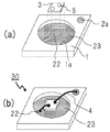
この実施例の発光装置は、図2(a)及び(b)に示したように、その表面に凹部1aが形成されたAl2O3からなるパッケージ1と、その凹部の底面である1a絶縁基板と、絶縁基板1の上面の一部を被覆するAgからなる金属部材2、2aと、表面に正及び負の電極5を備え、裏面全面にAl金属膜(図示せず)が形成された発光素子3とを備えて構成される。
凹部内の金属部材2には、絶縁基板1が一部露出した露出領域1bが、濡れ性の悪い領域として形成されている。この露出領域1bは、発光素子3に形成された金属膜の周縁部3a直下から発光素子3の内側に配置されている。
Example 1
As shown in FIGS. 2A and 2B, the light emitting device of this embodiment has a package 1 made of Al 2 O 3 having a
In the
この発光装置は、以下のようにして製造することができる。
まず、長さ800μm、幅800μmの正方形の発光素子3を準備する。
この発光素子3は、青色系に発光する窒化物系半導体からなり、波長465nmの光を放射する。発光素子3の表面には、正及び負の電極5がそれぞれ形成されている。また、裏面には、Al金属膜、半田材料の拡散を防止するWバリア膜、半田に濡れるPt膜がスパッタ法により、全面に、この順で積層されている。
This light emitting device can be manufactured as follows.
First, a square light-emitting element 3 having a length of 800 μm and a width of 800 μm is prepared.
The light emitting element 3 is made of a nitride semiconductor that emits blue light, and emits light having a wavelength of 465 nm. Positive and
次いで、絶縁基板1として、長さ3.0mm、幅3.0mm、厚さ1.0mmのAl2O3基板(波長465nmの光の反射率が約70%)を準備する。この絶縁基板1の中央には、直径2.5mm、深さ0.6mmの円筒状の凹部1aが形成されている。
Next, an Al 2 O 3 substrate (the reflectance of light having a wavelength of 465 nm is approximately 70%) having a length of 3.0 mm, a width of 3.0 mm, and a thickness of 1.0 mm is prepared as the insulating substrate 1. A
この絶縁基板1の上面の一部及び凹部1aの底面に、印刷法により、W膜を形成し、そのW膜を焼結させた後、膜厚約7μmのAgメッキを施すことにより、Agからなる金属部材2、2aを形成する。この金属部材は、波長465nmの光の反射率が約95%である。
凹部1aの底面に形成した金属部材2は、ダイパッドと、LED発光時に絶縁基板1方向へ放射する光に対する反射と、発光素子3の一方(例えば、負)の電極と接続するワイヤボンドパッドとの、3つの機能を兼ねている。ダイパッド機能は、主として、発光素子3の大きさに対応する領域内の金属部材2が果たし、反射機能及びワイヤーボンドパット機能は、発光素子3の外周部分の金属部材2が果たす。
また、絶縁基板1の上面の金属部材2aは、発光素子3の他方(例えば、正)の電極と接続するワイヤボンドパッド機能を果たす。
A W film is formed on a part of the upper surface of the insulating substrate 1 and the bottom surface of the
The
Further, the
凹部1aの底面の金属部材2には、絶縁基板1であるAl2O3を露出させる露出領域1bが形成されている。この露出領域1bは、発光素子3(厳密には、発光素子3裏面の金属膜)の周縁部3aから発光素子3の内側に広がる領域として配置され、それぞれ幅50μm、長さ600μmの矩形の領域である。この露出領域1bは、発光素子3の周縁部3aの各辺の中央部分に、それぞれ独立して合計4個配置されている。
On the
続いて、ダイパッドに相当する金属部材2上に、ダイボンド部材(図示せず)として、Auが80wt%、Au−Su粒子とフラックスからなるペーストを適量塗布し、その上に発光素子3を載置し、仮固定する。
Subsequently, on the
その後、発光素子3を所定の領域に高精度にアライメントするために、発光素子3が仮固定された絶縁基板1を、340℃のリフロー炉に通して、ペースト溶剤であるフラックスを揮発させ、Au−Snを溶融し、さらに凝固させて、金属部材2のダイパットに相当する領域に接着融接合させる。
その後、準水系洗浄剤にてフラックスを洗浄する。
Thereafter, in order to align the light emitting element 3 with high accuracy in a predetermined region, the insulating substrate 1 on which the light emitting element 3 is temporarily fixed is passed through a reflow furnace at 340 ° C. to volatilize the flux as the paste solvent, and Au -Sn is melted, further solidified, and bonded and bonded to a region corresponding to the die pad of the
Thereafter, the flux is washed with a semi-aqueous detergent.
次に、発光素子3上面の正及び負の電極と、各電極に対応するワイヤボンドパッドとの間に、ワイヤ4にて配線する。
続いて、透光性被覆材(図示せず)として、蛍光物質が含有されたシリコーン樹脂を、発光素子3の主光取り出し面と側面とに形成する。
Next, the wires 4 are wired between the positive and negative electrodes on the upper surface of the light emitting element 3 and the wire bond pads corresponding to the respective electrodes.
Subsequently, as a translucent coating material (not shown), a silicone resin containing a fluorescent material is formed on the main light extraction surface and side surfaces of the light emitting element 3.
このようにして得られた発光装置について、実装精度のばらつきを測定したところ、4σで30μmであった。また、350mWで駆動させた場合の光束を測定したところ、約45lmであった。
この結果から、本実施例の発光装置は、発光素子実装時に、ダイパッドとして機能する金属部材2と、発光素子3の搭載位置を厳密に制御し得る濡れ性の悪い領域である絶縁基板の露出領域1bとにより、セルフアライメント効果が十分に発揮されるため、実装精度を著しく向上させることができる。従って、発光素子3の発光時に、絶縁基板1方向へ放射する光を、発光素子3の外周部に存在する金属部材2によって効率よく反射させることができるために、光の取り出し効率を向上させることができる。
The variation in mounting accuracy of the light emitting device thus obtained was measured and found to be 30 μm at 4σ. Further, when the luminous flux was measured when driven at 350 mW, it was about 45 lm.
From this result, in the light emitting device of this example, when the light emitting element is mounted, the
比較例1
比較例1として、図3(a)及び(b)に示すように、絶縁基板1の凹部1a底面に形成する金属部材12の形状を、発光素子3の大きさと同じ形状とした以外、実質的に実施例1と同様の構造の発光装置を形成した。この発光装置では、金属部材12が形成されていない凹部1a底面は、絶縁基板が露出している。
Comparative Example 1
As Comparative Example 1, as shown in FIGS. 3A and 3B, the shape of the
この発光装置では、金属部材12は、実施例1における反射機能を有さない。
従って、この発光装置を製造する際に、セルフアライメント効果は得られるものの、実施例1に比べて発光素子3の発光時に、絶縁基板1方向へ放射する光の損失が大きくなった。この場合の光束を実施例1と同様に測定したところ、約36lmであり、実施例1の発光装置より20%程度、光損失が生じた。
また、実施例1と同様に実装ばらつきを測定したところ、4σで50〜70μm程度であった。
In this light emitting device, the
Therefore, when this light-emitting device is manufactured, although the self-alignment effect is obtained, the loss of light emitted toward the insulating substrate 1 is larger when the light-emitting element 3 emits light than in Example 1. The luminous flux in this case was measured in the same manner as in Example 1. As a result, it was about 36 lm, and an optical loss of about 20% occurred from the light emitting device of Example 1.
Further, when the mounting variation was measured in the same manner as in Example 1, it was about 50 to 70 μm at 4σ.
比較例2
比較例2として、図4(a)及び(b)に示すように、絶縁基板1の凹部1a底面に形成する金属部材22の形状を、発光素子3の大きさと同じ形状とし、さらに発光素子の外周部に、金属部材22と50μm隔離して、金属膜23を形成した以外、実質的に実施例1と同様の構造の発光素子を形成した。
Comparative Example 2
As Comparative Example 2, as shown in FIGS. 4A and 4B, the shape of the
この発光装置では、ダイパッド部として機能する金属部材22と金属膜23との間に、絶縁基板1の表面が露出している。
従って、この発光装置を製造する際には、セルフアライメント効果は得られ、比較例1に比べると、金属膜23の効果により、発光素子3の発光時に、絶縁基板1方向へ放射する光の損失が緩和される。しかし、この発光装置の光束を測定したところ、約40lmであり、実施例1の発光装置より10%程度、光損失が生じた。
また、実施例1と同様に実装ばらつきを測定したところ、4σで50〜70μm程度であった。
In this light emitting device, the surface of the insulating substrate 1 is exposed between the
Therefore, when manufacturing this light-emitting device, a self-alignment effect can be obtained. Compared with Comparative Example 1, the loss of light emitted toward the insulating substrate 1 when the light-emitting element 3 emits light due to the effect of the
Further, when the mounting variation was measured in the same manner as in Example 1, it was about 50 to 70 μm at 4σ.
照明用光源、各種インジケーター用光源、車載用光源、ディスプレイ用光源、液晶のバックライト用光源、信号機、車載部品、看板用チャンネルレターなど、種々の光源に使用することができる。 It can be used for various light sources such as illumination light sources, various indicator light sources, in-vehicle light sources, display light sources, liquid crystal backlight light sources, traffic lights, in-vehicle components, and signboard channel letters.
10 発光装置
1 絶縁基板
1a 凹部
1b、11b、21b、31b、41b 絶縁基板の露出領域
2、2a 金属部材
3 発光素子
3a 周縁部
4 ワイヤー
5 電極
DESCRIPTION OF
Claims (11)
前記発光素子が載置され、該発光素子の下部からその周辺部にわたって配置された金属部材と、
前記金属部材と前記発光素子の金属膜とを接着する金属からなるダイボンド部材とを有し、
前記発光素子の下方であって、前記発光素子底面の金属膜の周縁部から始まって前記発光素子の内側に向かって広がるように、かつ前記ダイボンド部材の周辺部に、前記金属部材よりも前記ダイボンド部材に対して濡れ性の悪い領域が配置されていることを特徴とする発光装置。 A light emitting device having a metal film formed on the bottom;
A metal member on which the light emitting element is mounted and disposed from the lower part of the light emitting element to the periphery thereof;
A die-bonding member made of a metal that bonds the metal member and the metal film of the light-emitting element;
The die bond is located below the light emitting element, starting from the peripheral edge of the metal film on the bottom surface of the light emitting element and extending toward the inside of the light emitting element , and at the periphery of the die bond member rather than the metal member. An area having poor wettability with respect to a member is disposed.
前記基板上に形成された金属部材と、
底部に金属膜が形成された発光素子と、
前記金属部材と前記発光素子の金属膜とを接着する金属からなるダイボンド部材とを備えた発光装置であって、
前記発光素子の下方、かつ前記発光素子底面の金属膜の周縁部から始まって前記発光素子の内側に向かって広がるように、前記基板の一部が前記金属部材から露出してなることを特徴とする発光装置。 A substrate,
A metal member formed on the substrate;
A light emitting device having a metal film formed on the bottom;
A light-emitting device comprising a die-bonding member made of a metal that bonds the metal member and a metal film of the light-emitting element,
A part of the substrate is exposed from the metal member so as to start from the peripheral portion of the metal film on the bottom surface of the light emitting element and toward the inside of the light emitting element. Light-emitting device.
Priority Applications (1)
| Application Number | Priority Date | Filing Date | Title |
|---|---|---|---|
| JP2006298982A JP5125060B2 (en) | 2006-11-02 | 2006-11-02 | Light emitting device |
Applications Claiming Priority (1)
| Application Number | Priority Date | Filing Date | Title |
|---|---|---|---|
| JP2006298982A JP5125060B2 (en) | 2006-11-02 | 2006-11-02 | Light emitting device |
Publications (3)
| Publication Number | Publication Date |
|---|---|
| JP2008117900A JP2008117900A (en) | 2008-05-22 |
| JP2008117900A5 JP2008117900A5 (en) | 2009-11-19 |
| JP5125060B2 true JP5125060B2 (en) | 2013-01-23 |
Family
ID=39503614
Family Applications (1)
| Application Number | Title | Priority Date | Filing Date |
|---|---|---|---|
| JP2006298982A Active JP5125060B2 (en) | 2006-11-02 | 2006-11-02 | Light emitting device |
Country Status (1)
| Country | Link |
|---|---|
| JP (1) | JP5125060B2 (en) |
Families Citing this family (7)
| Publication number | Priority date | Publication date | Assignee | Title |
|---|---|---|---|---|
| JP2013041931A (en) * | 2011-08-12 | 2013-02-28 | Ricoh Co Ltd | Optical element package, surface light emitting laser module, optical scanner device, and image formation device |
| JP6079223B2 (en) * | 2011-12-28 | 2017-02-15 | 日亜化学工業株式会社 | Package molded body for light emitting device |
| US9093621B2 (en) | 2011-12-28 | 2015-07-28 | Nichia Corporation | Molded package for light emitting device |
| JP6191308B2 (en) | 2012-07-27 | 2017-09-06 | 日亜化学工業株式会社 | Light emitting device for line light source |
| US9627591B2 (en) | 2015-02-25 | 2017-04-18 | Nichia Corporation | Mounting substrate and electronic device including the same |
| JP6582827B2 (en) * | 2015-09-30 | 2019-10-02 | 日亜化学工業株式会社 | Substrate, light emitting device, and method of manufacturing light emitting device |
| JP7064324B2 (en) * | 2017-12-18 | 2022-05-10 | スタンレー電気株式会社 | A semiconductor light emitting device and a method for manufacturing a semiconductor light emitting device using the semiconductor light emitting device. |
Family Cites Families (8)
| Publication number | Priority date | Publication date | Assignee | Title |
|---|---|---|---|---|
| JPH0470363A (en) * | 1990-07-02 | 1992-03-05 | Alps Electric Co Ltd | Optical writing head |
| JP2985830B2 (en) * | 1997-05-19 | 1999-12-06 | 日本電気株式会社 | Optical module and manufacturing method thereof |
| JPH11161197A (en) * | 1997-11-25 | 1999-06-18 | Matsushita Electric Ind Co Ltd | Picture display device |
| JP4114364B2 (en) * | 2001-11-08 | 2008-07-09 | 日亜化学工業株式会社 | Light emitting device and manufacturing method thereof |
| JP3924481B2 (en) * | 2002-03-08 | 2007-06-06 | ローム株式会社 | Semiconductor device using semiconductor chip |
| JP2005038970A (en) * | 2003-07-17 | 2005-02-10 | Ricoh Co Ltd | Sub-mount and semiconductor laser device |
| JP4632690B2 (en) * | 2004-05-11 | 2011-02-16 | スタンレー電気株式会社 | Semiconductor light emitting device and manufacturing method thereof |
| JP4384073B2 (en) * | 2005-03-17 | 2009-12-16 | 第一電子工業株式会社 | Manufacturing method of electronic parts |
-
2006
- 2006-11-02 JP JP2006298982A patent/JP5125060B2/en active Active
Also Published As
| Publication number | Publication date |
|---|---|
| JP2008117900A (en) | 2008-05-22 |
Similar Documents
| Publication | Publication Date | Title |
|---|---|---|
| US8450764B2 (en) | Semiconductor light-emitting apparatus and method of fabricating the same | |
| JP4826470B2 (en) | Light emitting device | |
| JP4935514B2 (en) | Light emitting device | |
| JP5691681B2 (en) | Light emitting device | |
| JP5326229B2 (en) | Light emitting device | |
| JP4882634B2 (en) | Light emitting device | |
| TW201042785A (en) | LED package with increased feature sizes | |
| JP5082710B2 (en) | Light emitting device | |
| JP5125060B2 (en) | Light emitting device | |
| JP6064606B2 (en) | Light emitting device | |
| JP2009065002A (en) | Light-emitting apparatus | |
| JP4940900B2 (en) | Mounting parts and semiconductor devices | |
| JP5256591B2 (en) | Light emitting device | |
| JP2007280983A (en) | Light-emitting device | |
| JP5055837B2 (en) | Light emitting device | |
| JP6191214B2 (en) | Light emitting device | |
| JP5030009B2 (en) | Light emitting device | |
| JP2008198962A (en) | Light emitting device and its manufacturing method | |
| JP2017017162A (en) | Light-emitting device | |
| JP5817390B2 (en) | Light emitting device | |
| JP2009081460A (en) | Semiconductor light-emitting device equipped with metallic package | |
| JP2010205788A (en) | Light emitting device | |
| JP5857585B2 (en) | Light emitting device | |
| JP5870582B2 (en) | Light emitting device | |
| JP2015026872A (en) | Light-emitting device, and method of manufacturing the same |
Legal Events
| Date | Code | Title | Description |
|---|---|---|---|
| A521 | Request for written amendment filed |
Free format text: JAPANESE INTERMEDIATE CODE: A523 Effective date: 20091006 |
|
| A621 | Written request for application examination |
Free format text: JAPANESE INTERMEDIATE CODE: A621 Effective date: 20091006 |
|
| A977 | Report on retrieval |
Free format text: JAPANESE INTERMEDIATE CODE: A971007 Effective date: 20111109 |
|
| A131 | Notification of reasons for refusal |
Free format text: JAPANESE INTERMEDIATE CODE: A131 Effective date: 20111115 |
|
| A521 | Request for written amendment filed |
Free format text: JAPANESE INTERMEDIATE CODE: A523 Effective date: 20120110 |
|
| A131 | Notification of reasons for refusal |
Free format text: JAPANESE INTERMEDIATE CODE: A131 Effective date: 20120529 |
|
| A521 | Request for written amendment filed |
Free format text: JAPANESE INTERMEDIATE CODE: A523 Effective date: 20120727 |
|
| TRDD | Decision of grant or rejection written | ||
| A01 | Written decision to grant a patent or to grant a registration (utility model) |
Free format text: JAPANESE INTERMEDIATE CODE: A01 Effective date: 20121002 |
|
| A01 | Written decision to grant a patent or to grant a registration (utility model) |
Free format text: JAPANESE INTERMEDIATE CODE: A01 |
|
| A61 | First payment of annual fees (during grant procedure) |
Free format text: JAPANESE INTERMEDIATE CODE: A61 Effective date: 20121015 |
|
| R150 | Certificate of patent or registration of utility model |
Free format text: JAPANESE INTERMEDIATE CODE: R150 Ref document number: 5125060 Country of ref document: JP Free format text: JAPANESE INTERMEDIATE CODE: R150 |
|
| FPAY | Renewal fee payment (event date is renewal date of database) |
Free format text: PAYMENT UNTIL: 20151109 Year of fee payment: 3 |
|
| R250 | Receipt of annual fees |
Free format text: JAPANESE INTERMEDIATE CODE: R250 |
|
| R250 | Receipt of annual fees |
Free format text: JAPANESE INTERMEDIATE CODE: R250 |
|
| R250 | Receipt of annual fees |
Free format text: JAPANESE INTERMEDIATE CODE: R250 |
|
| R250 | Receipt of annual fees |
Free format text: JAPANESE INTERMEDIATE CODE: R250 |
|
| R250 | Receipt of annual fees |
Free format text: JAPANESE INTERMEDIATE CODE: R250 |
|
| R250 | Receipt of annual fees |
Free format text: JAPANESE INTERMEDIATE CODE: R250 |
|
| R250 | Receipt of annual fees |
Free format text: JAPANESE INTERMEDIATE CODE: R250 |
|
| R250 | Receipt of annual fees |
Free format text: JAPANESE INTERMEDIATE CODE: R250 |