JP5123573B2 - Semiconductor light emitting device and manufacturing method thereof - Google Patents
Semiconductor light emitting device and manufacturing method thereof Download PDFInfo
- Publication number
- JP5123573B2 JP5123573B2 JP2007156381A JP2007156381A JP5123573B2 JP 5123573 B2 JP5123573 B2 JP 5123573B2 JP 2007156381 A JP2007156381 A JP 2007156381A JP 2007156381 A JP2007156381 A JP 2007156381A JP 5123573 B2 JP5123573 B2 JP 5123573B2
- Authority
- JP
- Japan
- Prior art keywords
- layer
- metal
- light emitting
- disposed
- semiconductor light
- Prior art date
- Legal status (The legal status is an assumption and is not a legal conclusion. Google has not performed a legal analysis and makes no representation as to the accuracy of the status listed.)
- Expired - Fee Related
Links
- 239000004065 semiconductor Substances 0.000 title claims description 197
- 238000004519 manufacturing process Methods 0.000 title claims description 75
- 229910052751 metal Inorganic materials 0.000 claims description 405
- 239000002184 metal Substances 0.000 claims description 405
- 229910001218 Gallium arsenide Inorganic materials 0.000 claims description 215
- 239000000758 substrate Substances 0.000 claims description 209
- 238000005253 cladding Methods 0.000 claims description 90
- 238000000034 method Methods 0.000 claims description 53
- 229910052710 silicon Inorganic materials 0.000 claims description 41
- 239000010703 silicon Substances 0.000 claims description 41
- XUIMIQQOPSSXEZ-UHFFFAOYSA-N Silicon Chemical compound [Si] XUIMIQQOPSSXEZ-UHFFFAOYSA-N 0.000 claims description 40
- 239000010936 titanium Substances 0.000 claims description 20
- 229910045601 alloy Inorganic materials 0.000 claims description 18
- 239000000956 alloy Substances 0.000 claims description 18
- RTAQQCXQSZGOHL-UHFFFAOYSA-N Titanium Chemical compound [Ti] RTAQQCXQSZGOHL-UHFFFAOYSA-N 0.000 claims description 16
- 229910052719 titanium Inorganic materials 0.000 claims description 16
- 230000000903 blocking effect Effects 0.000 claims description 12
- 238000005530 etching Methods 0.000 claims description 10
- 229910000990 Ni alloy Inorganic materials 0.000 claims description 9
- 229910052782 aluminium Inorganic materials 0.000 claims description 8
- 229910052709 silver Inorganic materials 0.000 claims description 8
- 229910052814 silicon oxide Inorganic materials 0.000 claims description 6
- 238000000059 patterning Methods 0.000 claims description 5
- 229910052581 Si3N4 Inorganic materials 0.000 claims description 3
- 229910020286 SiOxNy Inorganic materials 0.000 claims description 3
- VYPSYNLAJGMNEJ-UHFFFAOYSA-N Silicium dioxide Chemical compound O=[Si]=O VYPSYNLAJGMNEJ-UHFFFAOYSA-N 0.000 claims description 3
- 229910052804 chromium Inorganic materials 0.000 claims description 3
- 229910052759 nickel Inorganic materials 0.000 claims description 3
- HQVNEWCFYHHQES-UHFFFAOYSA-N silicon nitride Chemical compound N12[Si]34N5[Si]62N3[Si]51N64 HQVNEWCFYHHQES-UHFFFAOYSA-N 0.000 claims description 3
- 229910052721 tungsten Inorganic materials 0.000 claims description 3
- 229910000980 Aluminium gallium arsenide Inorganic materials 0.000 description 30
- 230000004048 modification Effects 0.000 description 19
- 238000012986 modification Methods 0.000 description 19
- 229910015363 Au—Sn Inorganic materials 0.000 description 12
- 230000031700 light absorption Effects 0.000 description 11
- 230000004888 barrier function Effects 0.000 description 9
- 238000005516 engineering process Methods 0.000 description 8
- 238000010586 diagram Methods 0.000 description 7
- 238000009792 diffusion process Methods 0.000 description 5
- 239000000463 material Substances 0.000 description 5
- 238000002310 reflectometry Methods 0.000 description 4
- 238000010521 absorption reaction Methods 0.000 description 3
- 230000007423 decrease Effects 0.000 description 3
- BASFCYQUMIYNBI-UHFFFAOYSA-N platinum Chemical compound [Pt] BASFCYQUMIYNBI-UHFFFAOYSA-N 0.000 description 3
- 238000004544 sputter deposition Methods 0.000 description 3
- 238000001771 vacuum deposition Methods 0.000 description 3
- QGZKDVFQNNGYKY-UHFFFAOYSA-N Ammonia Chemical compound N QGZKDVFQNNGYKY-UHFFFAOYSA-N 0.000 description 2
- KRHYYFGTRYWZRS-UHFFFAOYSA-N Fluorane Chemical compound F KRHYYFGTRYWZRS-UHFFFAOYSA-N 0.000 description 2
- VEXZGXHMUGYJMC-UHFFFAOYSA-N Hydrochloric acid Chemical compound Cl VEXZGXHMUGYJMC-UHFFFAOYSA-N 0.000 description 2
- 238000001579 optical reflectometry Methods 0.000 description 2
- WFKWXMTUELFFGS-UHFFFAOYSA-N tungsten Chemical compound [W] WFKWXMTUELFFGS-UHFFFAOYSA-N 0.000 description 2
- 239000010937 tungsten Substances 0.000 description 2
- JMASRVWKEDWRBT-UHFFFAOYSA-N Gallium nitride Chemical compound [Ga]#N JMASRVWKEDWRBT-UHFFFAOYSA-N 0.000 description 1
- MHAJPDPJQMAIIY-UHFFFAOYSA-N Hydrogen peroxide Chemical compound OO MHAJPDPJQMAIIY-UHFFFAOYSA-N 0.000 description 1
- 229910000577 Silicon-germanium Inorganic materials 0.000 description 1
- 239000000853 adhesive Substances 0.000 description 1
- 230000001070 adhesive effect Effects 0.000 description 1
- 229910021529 ammonia Inorganic materials 0.000 description 1
- 230000015572 biosynthetic process Effects 0.000 description 1
- 238000005229 chemical vapour deposition Methods 0.000 description 1
- 238000010438 heat treatment Methods 0.000 description 1
- 239000011810 insulating material Substances 0.000 description 1
- 238000009413 insulation Methods 0.000 description 1
- 230000008018 melting Effects 0.000 description 1
- 238000002844 melting Methods 0.000 description 1
- 238000001451 molecular beam epitaxy Methods 0.000 description 1
- ZODDGFAZWTZOSI-UHFFFAOYSA-N nitric acid;sulfuric acid Chemical compound O[N+]([O-])=O.OS(O)(=O)=O ZODDGFAZWTZOSI-UHFFFAOYSA-N 0.000 description 1
- 229910052697 platinum Inorganic materials 0.000 description 1
- 229910052594 sapphire Inorganic materials 0.000 description 1
- 239000010980 sapphire Substances 0.000 description 1
- 229910021332 silicide Inorganic materials 0.000 description 1
- FVBUAEGBCNSCDD-UHFFFAOYSA-N silicide(4-) Chemical compound [Si-4] FVBUAEGBCNSCDD-UHFFFAOYSA-N 0.000 description 1
- 150000003376 silicon Chemical class 0.000 description 1
- 238000005245 sintering Methods 0.000 description 1
Images


Classifications
-
- H—ELECTRICITY
- H01—ELECTRIC ELEMENTS
- H01L—SEMICONDUCTOR DEVICES NOT COVERED BY CLASS H10
- H01L33/00—Semiconductor devices having potential barriers specially adapted for light emission; Processes or apparatus specially adapted for the manufacture or treatment thereof or of parts thereof; Details thereof
- H01L33/005—Processes
- H01L33/0093—Wafer bonding; Removal of the growth substrate
-
- H—ELECTRICITY
- H01—ELECTRIC ELEMENTS
- H01L—SEMICONDUCTOR DEVICES NOT COVERED BY CLASS H10
- H01L2933/00—Details relating to devices covered by the group H01L33/00 but not provided for in its subgroups
- H01L2933/0008—Processes
- H01L2933/0016—Processes relating to electrodes
-
- H—ELECTRICITY
- H01—ELECTRIC ELEMENTS
- H01L—SEMICONDUCTOR DEVICES NOT COVERED BY CLASS H10
- H01L33/00—Semiconductor devices having potential barriers specially adapted for light emission; Processes or apparatus specially adapted for the manufacture or treatment thereof or of parts thereof; Details thereof
- H01L33/02—Semiconductor devices having potential barriers specially adapted for light emission; Processes or apparatus specially adapted for the manufacture or treatment thereof or of parts thereof; Details thereof characterised by the semiconductor bodies
- H01L33/20—Semiconductor devices having potential barriers specially adapted for light emission; Processes or apparatus specially adapted for the manufacture or treatment thereof or of parts thereof; Details thereof characterised by the semiconductor bodies with a particular shape, e.g. curved or truncated substrate
- H01L33/22—Roughened surfaces, e.g. at the interface between epitaxial layers
-
- H—ELECTRICITY
- H01—ELECTRIC ELEMENTS
- H01L—SEMICONDUCTOR DEVICES NOT COVERED BY CLASS H10
- H01L33/00—Semiconductor devices having potential barriers specially adapted for light emission; Processes or apparatus specially adapted for the manufacture or treatment thereof or of parts thereof; Details thereof
- H01L33/36—Semiconductor devices having potential barriers specially adapted for light emission; Processes or apparatus specially adapted for the manufacture or treatment thereof or of parts thereof; Details thereof characterised by the electrodes
- H01L33/38—Semiconductor devices having potential barriers specially adapted for light emission; Processes or apparatus specially adapted for the manufacture or treatment thereof or of parts thereof; Details thereof characterised by the electrodes with a particular shape
- H01L33/387—Semiconductor devices having potential barriers specially adapted for light emission; Processes or apparatus specially adapted for the manufacture or treatment thereof or of parts thereof; Details thereof characterised by the electrodes with a particular shape with a plurality of electrode regions in direct contact with the semiconductor body and being electrically interconnected by another electrode layer
-
- H—ELECTRICITY
- H01—ELECTRIC ELEMENTS
- H01L—SEMICONDUCTOR DEVICES NOT COVERED BY CLASS H10
- H01L33/00—Semiconductor devices having potential barriers specially adapted for light emission; Processes or apparatus specially adapted for the manufacture or treatment thereof or of parts thereof; Details thereof
- H01L33/36—Semiconductor devices having potential barriers specially adapted for light emission; Processes or apparatus specially adapted for the manufacture or treatment thereof or of parts thereof; Details thereof characterised by the electrodes
- H01L33/40—Materials therefor
- H01L33/405—Reflective materials
-
- H—ELECTRICITY
- H01—ELECTRIC ELEMENTS
- H01L—SEMICONDUCTOR DEVICES NOT COVERED BY CLASS H10
- H01L33/00—Semiconductor devices having potential barriers specially adapted for light emission; Processes or apparatus specially adapted for the manufacture or treatment thereof or of parts thereof; Details thereof
- H01L33/44—Semiconductor devices having potential barriers specially adapted for light emission; Processes or apparatus specially adapted for the manufacture or treatment thereof or of parts thereof; Details thereof characterised by the coatings, e.g. passivation layer or anti-reflective coating
- H01L33/46—Reflective coating, e.g. dielectric Bragg reflector
Landscapes
- Engineering & Computer Science (AREA)
- Manufacturing & Machinery (AREA)
- Computer Hardware Design (AREA)
- Microelectronics & Electronic Packaging (AREA)
- Power Engineering (AREA)
- Led Devices (AREA)
Description
本発明は、半導体発光素子およびその製造方法に関し、特に、金属反射層を備える発光ダイオードと不透明基板層をウェハボンディング技術によって、貼り付けて形成することを特徴とする半導体発光素子およびその製造方法に関する。 The present invention relates to a semiconductor light emitting device and a method for manufacturing the same, and more particularly, to a semiconductor light emitting device and a method for manufacturing the same, wherein a light emitting diode having a metal reflection layer and an opaque substrate layer are attached by wafer bonding technology. .
発光ダイオード(LED:Light Emitting Diode)を高輝度化するために、光の反射層として、基板と、多重量子井戸(MQW:Multi-Quantum Well)層からなる活性層との間に金属反射層を形成する構造が提案されている。このような金属反射層を形成する方法として、例えば、発光ダイオード層の基板のウェハボンディング(貼付け)技術が開示されている(例えば、特許文献1および特許文献2参照。)。
In order to increase the brightness of a light emitting diode (LED), a metal reflection layer is provided as a light reflection layer between a substrate and an active layer composed of a multi-quantum well (MQW) layer. The structure to be formed has been proposed. As a method for forming such a metal reflective layer, for example, a wafer bonding (sticking) technique for a substrate of a light emitting diode layer has been disclosed (see, for example,
特許文献1および特許文献2は、所望の機械的特性と透光性を有する発光ダイオードを製造することができ、かつ透明層と成長層との境界面の抵抗率を最小限にすることができる発光ダイオードの製造方法を提供することを目的とし、一時的成長基板上に発光ダイオード層を順次成長させ、比較的薄い層の発光ダイオード構造を形成後、一時的成長基板を除去し、一時的成長基板に代えてその位置に下層の緩衝層となる発光ダイオード層に導電性、透光性基板をウェハボンディングして発光ダイオードを製造することを特徴とする。特許文献1および特許文献2においては、貼付けに用いる基板にはGaPやサファイア等の透明なものを適用している。
図24乃至図26は、ウェハボンディング技術により形成した従来の半導体発光素子の模式的断面構造を示す。 24 to 26 show a schematic cross-sectional structure of a conventional semiconductor light emitting device formed by a wafer bonding technique.
例えば、従来の半導体発光素子は、図24に示すように、GaAs基板15上に配置されたAu-Sn合金層14と、Au-Sn合金層14上に配置されたバリアメタル層13と、バリアメタル層13上に配置されたp型クラッド層10と、p型クラッド層10上に配置されたMQW層9と、MQW層9上に配置されたn型クラッド層8と、n型クラッド層8上に配置されたウィンドウ層7とを備える。
For example, as shown in FIG. 24, a conventional semiconductor light emitting device includes an Au—
図24に示す従来の半導体発光素子は、貼付けに使われる金属は、Au−Sn合金である。このAu−Sn合金は融点が低いため、低温でLEDを構成するエピタキシャル成長層側のAu−Sn合金とGaAs基板15側のAu−Sn合金が溶け、貼り付けることができる。
In the conventional semiconductor light emitting device shown in FIG. 24, the metal used for pasting is an Au—Sn alloy. Since the Au—Sn alloy has a low melting point, the Au—Sn alloy on the epitaxial growth layer side and the Au—Sn alloy on the
しかし、Au−Sn合金層14を使用する場合、Snの熱拡散が起こるため、Snの拡散を防ぐために、図24に示すように、バリアメタル層13を入れる必要がある。また、Au−Sn合金層14は光の反射率が悪いという問題点がある。
However, when the Au—
例えば、従来の別の半導体発光素子は、図25に示すように、GaAs基板15上に配置された金属反射層16と、金属反射層16上に配置されたp型クラッド層10と、p型クラッド層10上に配置されたMQW層9と、MQW層9上に配置されたn型クラッド層8と、n型クラッド層8上に配置されたウィンドウ層7とを備える。図25に示す従来の半導体発光素子は、GaAs基板15を貼り付けて作った金属反射層16では、金属と半導体との界面で光の吸収が起こり、効率よく光を反射することができないという問題点がある。すなわち、p型クラッド層10と金属反射層16の界面で光の吸収が起こるという問題点がある。
For example, as shown in FIG. 25, another conventional semiconductor light emitting device includes a
半導体発光素子(LED)を高輝度化するには、光の反射層としてGaAs基板と活性層(MQW)の間に分布ブラック反射(DBR:Distributed Bragg Reflector)層を入れる方法もある。DBRを入れない構造のLEDでは、MQW層で発光した光がGaAs基板に吸収されてしまうために暗くなる。そのため、GaAs基板を用いるLEDを高輝度化するために、光の反射層としてDBRが用いられている。 In order to increase the brightness of a semiconductor light emitting device (LED), there is also a method in which a distributed black reflection (DBR) layer is provided between a GaAs substrate and an active layer (MQW) as a light reflection layer. In an LED without a DBR structure, light emitted from the MQW layer is absorbed by the GaAs substrate and becomes dark. Therefore, DBR is used as a light reflection layer in order to increase the brightness of LEDs using a GaAs substrate.
すなわち、従来の更に別の半導体発光素子は、図26に示すように、GaAs基板15上に配置されたDBR層19と、DBR層19上に配置されたp型クラッド層10と、p型クラッド層10上に配置されたMQW層9と、MQW層9上に配置されたn型クラッド層8と、n型クラッド層8上に配置されたウィンドウ層7とを備える。図26に示す従来の半導体発光素子は、GaAs基板15とMQW層9との間に光の反射層としてDBR層19を用いているが、DBR層19はある一方向から入射した光のみ反射し、入射角が変わるとDBRは光を反射せず、それ以外の角度から入射した光はDBR層19で反射せず透過してしまうという問題点がある。そのため、透過した光はGaAs基板15に吸収されてしまい、半導体発光素子(LED)の発光輝度が低下するという問題点がある。
That is, another conventional semiconductor light emitting device includes, as shown in FIG. 26, a
ウェハボンディング技術により形成した従来の半導体発光素子は、貼付けに使われる金属としてAu−Sn合金層を使用する場合、Snの熱拡散を防ぐために、バリアメタル層を入れる必要がある。また、Au−Sn合金層は光の反射率が悪い。 When a conventional semiconductor light emitting device formed by wafer bonding technology uses an Au—Sn alloy layer as a metal used for pasting, it is necessary to insert a barrier metal layer in order to prevent thermal diffusion of Sn. Further, the Au—Sn alloy layer has poor light reflectivity.
また、基板を貼り付けることによって金属反射層を形成したとしても、金属と半導体の界面で光の吸収が起こり、効率よく光を反射することができない。 Even if the metal reflective layer is formed by attaching the substrate, light absorption occurs at the interface between the metal and the semiconductor, and light cannot be efficiently reflected.
また、反射層としてDBR層を用いている場合、DBR層はある一方向から入射した光のみ反射し、入射角が変わるとDBR層で反射せず透過してしまい、GaAs基板に吸収されてしまい、LEDの発光輝度が低下する。 In addition, when a DBR layer is used as the reflective layer, the DBR layer reflects only light incident from one direction, and if the incident angle changes, it is transmitted without being reflected by the DBR layer and absorbed by the GaAs substrate. , LED emission brightness decreases.
さらに、ウェハボンディング技術により形成した従来の半導体発光素子は、半導体基板、絶縁膜、金属層を貼り付ける時に、熱膨張係数の違いや、密着性の問題があるために、高温にすると剥がれるという問題がある。 Furthermore, conventional semiconductor light-emitting elements formed by wafer bonding technology have problems of peeling when heated to high temperatures due to differences in thermal expansion coefficient and adhesion problems when a semiconductor substrate, insulating film, and metal layer are attached. There is.
さらに、ウェハボンディング技術の代りに、接着剤を用いて、半導体発光素子の積層体と半導体基板を貼り付ける半導体発光素子およびその製造構造についても開示されている(たとえば、特許文献3参照。)。
本発明の目的は、GaAsやSi等の不透明な半導体基板を用いて、ウェハボンディング技術を用いて、基板の貼付けを密着性良く行い、金属反射層を形成して高輝度の半導体発光素子およびその製造方法を提供することにある。 An object of the present invention is to use a wafer bonding technique with an opaque semiconductor substrate such as GaAs or Si, and to adhere the substrate with good adhesion, to form a metal reflective layer, and to provide a high-luminance semiconductor light-emitting element and its It is to provide a manufacturing method.
また、本発明の目的は、金属と半導体との間に透明な絶縁膜を入れることにより、半導体と金属との接触を避け、半導体と金属との界面での光の吸収を防ぎ、反射率の良い金属反射層を形成した、高輝度の半導体発光素子およびその製造方法を提供することにある。 Another object of the present invention is to prevent contact between the semiconductor and the metal by inserting a transparent insulating film between the metal and the semiconductor, prevent light absorption at the interface between the semiconductor and the metal, and improve the reflectance. An object of the present invention is to provide a high-luminance semiconductor light-emitting device having a good metal reflection layer and a method for manufacturing the same.
また、本発明の目的は、光の反射層にDBRではなく、金属層を用いて、あらゆる角度の光を反射させることが可能となり、高輝度の半導体発光素子およびその製造方法を提供することにある。 It is another object of the present invention to provide a high-intensity semiconductor light emitting device and a method for manufacturing the same, by using a metal layer instead of a DBR as a light reflection layer and reflecting light at any angle. is there.
上記目的を達成するための本発明の一態様によれば、表面に複数の溝部を形成したGaAs層と、前記GaAs層の前記表面,前記溝部の側壁および前記溝部の底面に配置された第1金属バッファ層と、前記第1金属バッファ層上に配置された第1金属層と、前記GaAs層の裏面に配置された第2金属バッファ層と、前記第2金属バッファ層の前記GaAs層と反対側の表面に配置された第2金属層とを備えるGaAs基板構造と、前記GaAs基板構造上に配置され、第3金属層と、前記第3金属層上に配置される金属コンタクト層と、前記金属コンタクト層上に配置されるp型クラッド層と、前記p型クラッド層に配置される多重量子井戸層と、前記多重量子井戸層上に配置されるn型クラッド層と、前記n型クラッド層上に配置されるウィンドウ層を備える発光ダイオード構造とから構成され、前記GaAs層の前記表面に配置された前記第1金属層および前記第3金属層を用いて、前記GaAs基板構造と、前記発光ダイオード構造を貼り付けるとともに、前記溝部の前記第1金属層と前記第3金属層との間にはエアギャップが存在することを特徴とする半導体発光素子が提供される。 According to one aspect of the present invention for achieving the above object, a GaAs layer having a plurality of grooves formed on a surface thereof, and a first surface disposed on the surface of the GaAs layer, the sidewall of the groove, and the bottom surface of the groove. A metal buffer layer; a first metal layer disposed on the first metal buffer layer; a second metal buffer layer disposed on a back surface of the GaAs layer; and the GaAs layer of the second metal buffer layer opposite to the GaAs layer A GaAs substrate structure comprising a second metal layer disposed on a side surface; a third metal layer disposed on the GaAs substrate structure; a metal contact layer disposed on the third metal layer; A p-type cladding layer disposed on the metal contact layer; a multiple quantum well layer disposed on the p-type cladding layer; an n-type cladding layer disposed on the multiple quantum well layer; and the n-type cladding layer Placed on The GaAs substrate structure and the light emitting diode structure are affixed using the first metal layer and the third metal layer disposed on the surface of the GaAs layer. In addition, there is provided a semiconductor light emitting device characterized in that an air gap exists between the first metal layer and the third metal layer of the groove.
本発明の他の態様によれば、表面に複数の溝部を形成したGaAs基板と、前記GaAs基板の前記表面,前記溝部の側壁および前記溝部の底面に配置される金属層と、前記GaAs基板の前記表面上の前記金属層上に配置され,パターニングされた金属コンタクト層および絶縁層と、パターニングされた前記金属コンタクト層および前記絶縁層上に配置されるp型クラッド層10と、前記p型クラッド層上に配置される多重量子井戸層と、前記多重量子井戸層上に配置されるn型クラッド層と、前記n型クラッド層上に配置されるウィンドウ層を備える発光ダイオード構造とから構成され、前記GaAs基板の前記表面上の前記金属層を用いて、前記GaAs基板と、前記発光ダイオード構造を貼り付けると共に、前記溝部の前記金属層と前記発光ダイオード構造との間にはエアギャップが存在することを特徴とする半導体発光素子が提供される。 According to another aspect of the present invention, a GaAs substrate having a plurality of grooves formed on a surface thereof, a metal layer disposed on the surface of the GaAs substrate, a side wall of the groove, and a bottom surface of the groove, A patterned metal contact layer and insulating layer disposed on the metal layer on the surface; a p-type cladding layer disposed on the patterned metal contact layer and insulating layer; and the p-type cladding. A light emitting diode structure comprising a multiple quantum well layer disposed on the layer, an n-type cladding layer disposed on the multiple quantum well layer, and a window layer disposed on the n-type cladding layer, The metal layer on the surface of the GaAs substrate is used to attach the GaAs substrate and the light emitting diode structure, and the metal layer in the groove Serial semiconductor light emitting device characterized by the presence of an air gap between the light emitting diode structure is provided.
本発明の他の態様によれば、表面に複数の溝部を形成したGaAs基板と、前記GaAs基板の前記表面,前記溝部の側壁および前記溝部の底面上に配置された第1金属層とを備えるGaAs基板構造と、当該GaAs基板構造上に配置され、第2金属層と、前記第2金属層上に配置されるp型クラッド層と、前記p型クラッド層上に配置される多重量子井戸層と、前記多重量子井戸層上に配置されるn型クラッド層と、前記n型クラッド層上に配置されるウィンドウ層を備える発光ダイオード構造とから構成され、前記GaAs基板の前記表面上の前記第1金属層および前記第2金属層を用いて、前記GaAs基板と、前記発光ダイオード構造を貼り付けると共に、前記溝部の前記第1金属層と前記発光ダイオード構造との間にはエアギャップが存在することを特徴とする半導体発光素子が提供される。 According to another aspect of the present invention, there is provided a GaAs substrate having a plurality of grooves formed on the surface, and a first metal layer disposed on the surface of the GaAs substrate, the sidewall of the groove, and the bottom surface of the groove. A GaAs substrate structure, a second metal layer disposed on the GaAs substrate structure, a p-type cladding layer disposed on the second metal layer, and a multiple quantum well layer disposed on the p-type cladding layer And an n-type cladding layer disposed on the multiple quantum well layer, and a light emitting diode structure comprising a window layer disposed on the n-type cladding layer, and the first layer on the surface of the GaAs substrate. The GaAs substrate and the light emitting diode structure are attached using one metal layer and the second metal layer, and an air gap is provided between the first metal layer and the light emitting diode structure in the groove. The semiconductor light emitting element characterized in that the flop is present is provided.
本発明の他の態様によれば、表面に複数の溝部を形成したシリコン基板と、前記シリコン基板の前記表面,前記溝部の側壁および前記溝部の底面上に配置されるチタン層と、前記チタン層上に配置される第1金属層とから構成されるシリコン基板構造と、前記第1金属層上に配置される第2金属層と、前記第2金属層上に配置され,パターニングされた金属コンタクト層および絶縁層と、パターニングされた前記金属コンタクト層および前記絶縁層上に配置され,露出された表面にフロスト処理領域を有するエピタキシャル成長層と、前記エピタキシャル成長層上に配置され,パターニングされたn型GaAs層と、前記n型GaAs層上に配置され,パターニングされた表面電極層とから構成されるLED構造とを備え、前記シリコン基板の前記表面上の前記第1金属層および前記第2金属層を用いて、前記シリコン基板構造と、前記発光ダイオード構造を貼り付けると共に、前記溝部の前記第1金属層と前記LED構造との間にはエアギャップが存在することを特徴とする半導体発光素子が提供される。 According to another aspect of the present invention, a silicon substrate having a plurality of grooves formed on a surface thereof, a titanium layer disposed on the surface of the silicon substrate, side walls of the grooves, and a bottom surface of the grooves, and the titanium layer A silicon substrate structure comprising a first metal layer disposed thereon, a second metal layer disposed on the first metal layer, and a metal contact disposed and patterned on the second metal layer A layer and an insulating layer; an epitaxial growth layer disposed on the patterned metal contact layer and the insulating layer and having a frosted region on the exposed surface; and an n-type GaAs disposed and patterned on the epitaxial growth layer An LED structure comprising a layer and a patterned surface electrode layer disposed on the n-type GaAs layer, and the silicon substrate Using the first metal layer and the second metal layer on the surface, the silicon substrate structure and the light emitting diode structure are pasted, and between the first metal layer and the LED structure in the groove. There is provided a semiconductor light emitting device characterized in that an air gap exists.
本発明の他の態様によれば、表面に複数の溝部を形成したGaAs基板と、前記GaAs基板の前記表面,前記溝部の側壁および前記溝部の底面上に配置される金属バッファ層と、前記金属バッファ層上に配置される第1金属層とから構成されるGaAs基板構造と、前記第1金属層上に配置される第2金属層と、前記第2金属層上に配置され,パターニングされた金属コンタクト層および絶縁層と、パターニングされた前記金属コンタクト層および前記絶縁層上に配置され,露出された表面にフロスト処理領域を有するエピタキシャル成長層と、前記エピタキシャル成長層上に配置され,パターニングされたn型GaAs層と、前記n型GaAs層上に配置され,パターニングされた表面電極層とから構成されるLED構造を備え、前記GaAs基板の前記表面上の前記第1金属層および前記第2金属層を用いて、前記GaAs基板構造と、前記発光ダイオード構造を貼り付けると共に、前記溝部の前記第1金属層上に配置される第2金属層と前記LED構造との間にはエアギャップが存在することを特徴とする半導体発光素子が提供される。 According to another aspect of the present invention, a GaAs substrate having a plurality of grooves formed on a surface thereof, a metal buffer layer disposed on the surface of the GaAs substrate, a side wall of the groove, and a bottom surface of the groove, the metal A GaAs substrate structure composed of a first metal layer disposed on the buffer layer, a second metal layer disposed on the first metal layer, and disposed and patterned on the second metal layer A metal contact layer and an insulating layer, an epitaxial growth layer disposed on the patterned metal contact layer and the insulating layer and having a frosted region on the exposed surface, and an n layer disposed on the epitaxial growth layer and patterned An LED structure comprising a p-type GaAs layer and a patterned surface electrode layer disposed on the n-type GaAs layer; The first metal layer and the second metal layer on the surface of the As substrate are used to attach the GaAs substrate structure and the light emitting diode structure, and are disposed on the first metal layer in the groove. A semiconductor light emitting device is provided in which an air gap exists between the second metal layer and the LED structure.
本発明の他の態様によれば、貼付け用の半導体基板構造、および貼付け用の発光ダイオード構造を準備する工程と、前記半導体基板構造においては、半導体基板の表面に複数の溝部を形成した後、前記半導体基板上に第1金属層を形成する工程と、前記発光ダイオード構造においては、GaAs基板上にAlInGaP層、n型GaAs層、エピタキシャル成長層を順次形成する工程と、前記エピタキシャル成長層上に、パターニングされた絶縁層に対して、金属コンタクト層および第2金属層を形成する工程と、前記半導体基板の前記表面上の前記第1金属層を用いて、前記半導体基板と、前記貼付け用のLED構造を熱圧着により貼り付けると共に、前記溝部の前記第1金属層と前記LED構造との間にはエアギャップを形成する工程と、前記GaAs基板をエッチングにより除去する工程と、前記AllnGaP層を除去する工程と、表面電極層をパターン形成する工程と、フロスト処理を実施して、前記表面電極層の直下の前記n型GaAs層以外の前記n型GaAs層の除去を行う工程とを有することを特徴とする半導体発光素子の製造方法が提供される。 According to another aspect of the present invention, a step of preparing a semiconductor substrate structure for pasting and a light emitting diode structure for pasting, and in the semiconductor substrate structure, after forming a plurality of grooves on the surface of the semiconductor substrate, Forming a first metal layer on the semiconductor substrate; in the light-emitting diode structure; sequentially forming an AlInGaP layer, an n-type GaAs layer, and an epitaxial growth layer on a GaAs substrate; and patterning on the epitaxial growth layer Forming a metal contact layer and a second metal layer on the insulating layer, and using the first metal layer on the surface of the semiconductor substrate, the semiconductor substrate and the LED structure for pasting And a step of forming an air gap between the first metal layer of the groove and the LED structure; The step of removing the GaAs substrate by etching, the step of removing the AllnGaP layer, the step of patterning the surface electrode layer, and performing a frosting process, except for the n-type GaAs layer immediately below the surface electrode layer And a step of removing the n-type GaAs layer. A method of manufacturing a semiconductor light emitting device is provided.
本発明の半導体発光素子およびその製造方法によれば、Au−Sn合金層によるSn拡散の問題を解決するために、Auからなる金属層を用いて、エピタキシャル成長層と半導体基板を、ウェハボンディング技術を用いて密着性良く貼り付けることにより、バリアメタルが不要となり、Auからなる金属層を用いることで光の反射率の良い金属反射層をLED側の構造に形成することができるので、LEDの高輝度化を図ることができる。 According to the semiconductor light emitting device and the method of manufacturing the same of the present invention, in order to solve the problem of Sn diffusion due to the Au—Sn alloy layer, the epitaxial growth layer and the semiconductor substrate are bonded to each other by using a metal layer made of Au. By using and sticking with good adhesion, a barrier metal becomes unnecessary, and by using a metal layer made of Au, a metal reflective layer with good light reflectivity can be formed in the structure on the LED side. Brightness can be achieved.
本発明の半導体発光素子およびその製造方法によれば、金属反射層と半導体層との間に透明な絶縁膜を入れることにより、半導体層と金属反射層との接触を避け、半導体層と金属反射層との界面における光の吸収を防ぎ、反射率の良い金属反射層を形成することができるので、LEDの高輝度化を図ることができる。 According to the semiconductor light emitting device and the method of manufacturing the same of the present invention, by placing a transparent insulating film between the metal reflection layer and the semiconductor layer, contact between the semiconductor layer and the metal reflection layer is avoided, and the semiconductor layer and the metal reflection are prevented. Since light absorption at the interface with the layer can be prevented and a metal reflective layer with good reflectance can be formed, the brightness of the LED can be increased.
本発明の半導体発光素子およびその製造方法によれば、GaAs基板への光の吸収を防ぐために、反射層に金属を用いて光を全反射させ、GaAs基板への吸収を防ぎ、あらゆる角度の光を反射することが可能になるので、LEDを高輝度化することができる。 According to the semiconductor light emitting device and the method of manufacturing the same of the present invention, in order to prevent the light absorption to the GaAs substrate, the reflection layer is made of a metal to totally reflect the light to prevent the light absorption at the GaAs substrate. Can be reflected, so that the brightness of the LED can be increased.
次に、図面を参照して、本発明の実施の形態を説明する。以下の図面の記載において、同一または類似の部分には同一または類似の符号を付している。ただし、図面は模式的なものであり、現実のものとは異なることに留意すべきである。また、図面相互間においても互いの寸法の関係や比率が異なる部分が含まれていることはもちろんである。 Next, embodiments of the present invention will be described with reference to the drawings. In the following description of the drawings, the same or similar parts are denoted by the same or similar reference numerals. However, it should be noted that the drawings are schematic and different from the actual ones. Moreover, it is a matter of course that portions having different dimensional relationships and ratios are included between the drawings.
また、以下に示す実施の形態は、この発明の技術的思想を具体化するための装置や方法を例示するものであって、この発明の技術的思想は、各構成部品の配置などを下記のものに特定するものでない。この発明の技術的思想は、特許請求の範囲において、種々の変更を加えることができる。 Further, the embodiment described below exemplifies an apparatus and a method for embodying the technical idea of the present invention. The technical idea of the present invention is the arrangement of each component as described below. It is not something specific. The technical idea of the present invention can be variously modified within the scope of the claims.
[第1の実施の形態]
(素子構造)
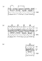
図1は、本発明の実施の形態に係る半導体発光素子およびその製造方法の原理説明図である。図1(a)は、GaAs基板の模式的断面構造図を示す。
[First embodiment]
(Element structure)
FIG. 1 is a diagram illustrating the principle of a semiconductor light emitting device and a method for manufacturing the same according to an embodiment of the present invention. FIG. 1A is a schematic cross-sectional structure diagram of a GaAs substrate.
本発明の実施の形態に係る半導体発光素子およびその製造方法に適用されるp型若しくはn型GaAs基板は、図1(a)に示すように、p型若しくはn型GaAs層(3、6)と、ピッチL,幅Wを有するストライプ状の溝が形成されたp型若しくはn型GaAs層(3、6)の表面に配置された金属層1とを備える。ストライプ溝の幅Wは、例えば約10μm,約30μm,或いは約60μm程度であり、ピッチLは、例えば約100μm,200μm,410μm,1000μm,或いは2000μm程度である。尚、溝部は、ストライプ形状に限定されるものではなく、格子状、ドット状、渦巻き状、六角形パターン形状などであってもよい。また、溝部の深さは、ストライプの幅Wと同程度若しくは、浅く形成される。
As shown in FIG. 1A, a p-type or n-type GaAs substrate (3, 6) is used for a p-type or n-type GaAs substrate applied to a semiconductor light emitting device and a method for manufacturing the same according to an embodiment of the present invention. And a
図1(b)は、図1(a)に示したGaAs基板と、LEDをウェハボンディング技術によって互いに貼り付けて形成した半導体発光素子の模式的断面構造を示す。LED側は、例えばエピタキシャル成長によって形成されたp型クラッド層10と、p型クラッド層10上に形成された金属層12で示されており、その他の活性層などは図示を省略している。GaAs層(3,6)の表面に配置された金属層1を用いて、GaAs基板と、LEDを貼り付けるとともに、溝部の金属層1と金属層12との間にはエアギャップ40が存在する。
FIG. 1B shows a schematic cross-sectional structure of a semiconductor light emitting element formed by bonding the GaAs substrate shown in FIG. 1A and an LED to each other by a wafer bonding technique. The LED side is shown by, for example, a p-
すなわち、このような溝部をGaAs基板表面に形成することによって、LEDをウェハボンディング技術によってGaAs基板に貼り付ける時に、空気の逃げ道を作り、さらに高温加熱時の熱膨張で生じる応力を緩和させることができる。結果として、半導体基板、絶縁膜、金属層の熱膨張係数の違いによる各層間の剥がれを防止することができる。 That is, by forming such a groove on the surface of the GaAs substrate, when the LED is attached to the GaAs substrate by wafer bonding technology, an air escape path can be created and stress generated by thermal expansion during high temperature heating can be reduced. it can. As a result, it is possible to prevent peeling between layers due to differences in thermal expansion coefficients of the semiconductor substrate, the insulating film, and the metal layer.
図1(c)は、さらにチップ化後の模式的断面構造図を示す。p型若しくはn型GaAs基板の表面に形成したストライプ状の溝部に形成されたエアギャップ40が完成したチップ内に含まれている。ピッチLが大きい場合には、エアギャップ40が完成したチップ内に含まれない場合もある。
FIG. 1C shows a schematic cross-sectional structure view after further chip formation. An
本発明の第1の実施の形態に係る半導体発光素子およびその製造方法に適用されるGaAs基板の導電型としては、p型、n型のいずれにおいても適用可能である。図2は、本発明の第1の実施の形態に係る半導体発光素子およびその製造方法に適用されるp型GaAs基板の模式的断面構造を示し、図3は、n型GaAs基板の模式的断面構造を示す。また、図4は、本発明の第1の実施の形態に係る半導体発光素子およびその製造方法に適用されるLEDの模式的断面構造を示す。 The conductivity type of the GaAs substrate applied to the semiconductor light emitting device and the manufacturing method thereof according to the first embodiment of the present invention can be applied to either p-type or n-type. FIG. 2 shows a schematic cross-sectional structure of a p-type GaAs substrate applied to the semiconductor light emitting device and the manufacturing method thereof according to the first embodiment of the present invention, and FIG. 3 shows a schematic cross-section of the n-type GaAs substrate. The structure is shown. FIG. 4 shows a schematic cross-sectional structure of an LED applied to the semiconductor light emitting device and the method for manufacturing the same according to the first embodiment of the present invention.
図5は、図2乃至図3に示したp型乃至n型GaAs基板と、図4に示したLEDをウェハボンディング技術によって互いに貼り付けて形成した本発明の第1の実施の形態に係る半導体発光素子の模式的断面構造を示す。 FIG. 5 shows a semiconductor according to the first embodiment of the present invention formed by bonding the p-type to n-type GaAs substrate shown in FIGS. 2 to 3 and the LED shown in FIG. 4 to each other by a wafer bonding technique. 1 shows a schematic cross-sectional structure of a light-emitting element.
本発明の第1の実施の形態に係る半導体発光素子およびその製造方法に適用されるp型GaAs基板は、図2に示すように、表面に複数の溝部を形成したp型GaAs層3と、p型GaAs層3の表面、溝部の側壁および溝部の底面に配置された金属バッファ層2と、金属バッファ層2上に配置された金属層1と、p型GaAs層3の裏面に配置された金属バッファ層4と、金属バッファ層4のp型GaAs層3と反対側の表面に配置された金属層5とを備える。
As shown in FIG. 2, the p-type GaAs substrate applied to the semiconductor light emitting device and the manufacturing method thereof according to the first embodiment of the present invention includes a p-
本発明の第1の実施の形態に係る半導体発光素子およびその製造方法に適用されるn型GaAs基板は、図3に示すように、表面に複数の溝部を形成したn型GaAs層6と、n型GaAs層6の表面、溝部の側壁および溝部の底面に配置された金属バッファ層2と、金属バッファ層2上に配置された金属層1と、n型GaAs層6の裏面に配置された金属バッファ層4と、金属バッファ層4のn型GaAs層6と反対側の表面に配置された金属層5とを備える。
As shown in FIG. 3, the n-type GaAs substrate applied to the semiconductor light emitting device and the manufacturing method thereof according to the first embodiment of the present invention includes an n-
図2の構造において、金属層1、5はいずれもAu層によって形成され、金属バッファ層2、4は、p型GaAs層3とコンタクトを取るために、例えばAuBe層によって形成可能である。また、図3の構造において、金属層1、5はいずれもAu層によって形成され、金属バッファ層2、4は、n型GaAs層6とコンタクトを取るために、例えばAuGe層によって形成可能である。
In the structure of FIG. 2, the
本発明の第1の実施の形態に係る半導体発光素子およびその製造方法に適用されるLEDの模式的断面構造は、図4に示すように、金属層12と、金属層12上に配置される金属コンタクト層11と、金属コンタクト層11上に配置されるp型クラッド層10と、p型クラッド層10上に配置されるMQW層9と、MQW層9上に配置されるn型クラッド層8と、n型クラッド層8上に配置されるウィンドウ層7を備える。
A schematic cross-sectional structure of an LED applied to the semiconductor light emitting device and the method for manufacturing the same according to the first embodiment of the present invention is arranged on a
図4の構造において、金属層12は、例えばAu層で形成される。また、金属コンタクト層は、例えばAuBe層あるいはAuBeとNiとの合金層などで形成される。p型クラッド層10は、例えばAlGaAs層若しくは導電型をp-型とするAlGaAs層と導電型をp+型とするAlGaAs層との多層構造によって形成され、厚さは、例えば約0.1μm程度である。MQW層9は、例えばGaAs/GaAlAs層からなるヘテロ接合ペアを約100ペア積層した多重量子井戸構造からなり、厚さは、例えば約1.6μm程度に形成される。n型クラッド層8は、例えばn型AlGaAs層によって形成され、厚さは、例えば約0.1μm程度である。ウィンドウ層7は、例えばAlGaAs層の多層構造とAlGaAs層の多層構造上に形成されたGaAs層からなり、全体の厚さは、約0.95μm程度である。
In the structure of FIG. 4, the
本発明の第1の実施の形態に係る半導体発光素子は、図5に示すように、図2乃至図3に示したp型乃至n型GaAs基板と、図4に示したLED構造をウェハボンディング技術によって互いに貼り付けて形成する。 As shown in FIG. 5, the semiconductor light emitting device according to the first embodiment of the present invention includes a p-type to n-type GaAs substrate shown in FIGS. 2 to 3 and an LED structure shown in FIG. Paste each other by technology.
すなわち、本発明の第1の実施の形態に係る半導体発光素子は、図5に示すように、表面に複数の溝部を形成したp(n)型GaAs層3(6)と、p(n)型GaAs層3(6)の表面、溝部の側壁および溝部の底面に配置された金属バッファ層2と、金属バッファ層2上に配置された金属層1と、p(n)型GaAs層3(6)の裏面に配置された金属バッファ層4と、金属バッファ層4のp(n)型GaAs層3(6)と反対側の表面に配置された金属層5とを備えるp(n)型GaAs基板構造と、当該p(n)型GaAs基板上に配置され、金属層12と、金属層12上に配置される金属コンタクト層11と、金属コンタクト層11上に配置されるp型クラッド層10と、p型クラッド層10上に配置されるMQW層9と、MQW層9上に配置されるn型クラッド層8と、n型クラッド層8上に配置されるウィンドウ層7を備えるLED構造とから構成される。
That is, as shown in FIG. 5, the semiconductor light emitting device according to the first embodiment of the present invention includes a p (n) type GaAs layer 3 (6) having a plurality of grooves formed on the surface, and p (n).
Au−Sn合金層からのSn拡散の問題点を解決するために、p(n)型GaAs層3(6)の表面に配置された金属層1および金属層12を用いて、p(n)型GaAs基板構造と、エピタキシャル成長層からなるLED構造を貼り付けると共に、溝部の第1金属層1と金属層12との間にはエアギャップ40が存在することにより、p(n)型GaAs層3(6)の表面に配置された金属層1と金属層12との密着性を良好に保つことができ、バリアメタルが不要で、反射率のよい金属反射層を形成することを可能にしている。
In order to solve the problem of Sn diffusion from the Au—Sn alloy layer, using the
金属反射層は、予め、LED構造側に配置された金属層12によって形成される。LEDからの放射光は、p型クラッド層10と、金属層12との界面によってミラー面が形成されるため、当該ミラー面において反射される。金属コンタクト層11は金属層12とp型クラッド層10とのオーミックコンタクトを取るための層であるが、金属層12とp型クラッド層10との界面に介在し、ミラー面の一部を形成している。
The metal reflection layer is formed in advance by the
本発明の第1の実施の形態に係る半導体発光素子は、図5に示すように、金属層1および金属層12をともにAu層によって形成することで、GaAs基板側の金属層1とエピタキシャル成長層からなるLED構造側の金属層12を熱圧着によって貼り付けることができる。
As shown in FIG. 5, the semiconductor light emitting device according to the first embodiment of the present invention is formed by forming both the
貼付けの条件は、例えば、約250℃〜700℃、望ましくは300℃〜400℃であり、熱圧着の圧力は、例えば、約10MPa〜20MPa程度である。エアギャップ40を設けたことにより、金属層1と金属層12の接触面積は、全面を密着させる構造に比較して、減少している。上記熱圧着の圧力は、結果として、エアギャップ40を設けたことにより、相対的に接触面積が低下した金属層1と金属層12の接触面積に加圧されることになり、金属層1と金属層12の熱圧着時において、貼り付け強度が高くなる。したがって、p(n)型GaAs基板構造と、エピタキシャル成長層からなるLED構造を貼り付けるに際して、エアギャップ40が存在することにより、p(n)型GaAs層3(6)の表面に配置された金属層1と金属層12との密着性を良好に保つことができる。
The pasting condition is, for example, about 250 ° C. to 700 ° C., desirably 300 ° C. to 400 ° C., and the pressure of thermocompression bonding is, for example, about 10 MPa to 20 MPa. By providing the
本発明の第1の実施の形態に係る半導体発光素子によれば、金属層1と金属層12との密着性を良好に保ちつつ、Auからなる金属層12を用いることで光の反射率の良い金属反射層をLED側の構造に形成することができるので、LEDの高輝度化を図ることができる。
According to the semiconductor light emitting device according to the first embodiment of the present invention, the light reflectance can be improved by using the
[第2の実施の形態]
(素子構造)
図6は、本発明の第2の実施の形態に係る半導体発光素子およびその製造方法に適用されるLEDの模式的断面構造を示す。また、図7は、本発明の第2の実施の形態の変形例に係る半導体発光素子およびその製造方法に適用されるLEDの模式的断面構造を示す。
[Second Embodiment]
(Element structure)
FIG. 6 shows a schematic cross-sectional structure of an LED applied to the semiconductor light emitting device and the method for manufacturing the same according to the second embodiment of the present invention. FIG. 7 shows a schematic cross-sectional structure of an LED applied to a semiconductor light emitting device and a method for manufacturing the same according to a modification of the second embodiment of the present invention.
図8は、p型乃至n型GaAs基板15と、図7に示したLEDをウェハボンディング技術によって互いに貼り付けて形成した本発明の第2の実施の形態に係る半導体発光素子の模式的断面構造を示す。尚、図8において、GaAs基板15上に配置される、例えばAu層からなる金属層は、図示を省略している。或いはまた、GaAs基板15上にはAu層などの金属層を配置せず、金属層12のみでGaAs基板15とLED構造を貼り付けることも可能である。
FIG. 8 is a schematic cross-sectional structure of a semiconductor light emitting device according to the second embodiment of the present invention formed by bonding the p-type to n-
本発明の第2の実施の形態に係る半導体発光素子およびその製造方法に適用されるLEDは、図6に示すように、金属層12と、金属層12上に配置され,パターニングされた金属コンタクト層11および絶縁層17と、パターニングされた金属コンタクト層11および絶縁層17上に配置されるp型クラッド層10と、p型クラッド層10上に配置されるMQW層9と、MQW層9上に配置されるn型クラッド層8と、n型クラッド層8上に配置されるウィンドウ層7を備える。
As shown in FIG. 6, the LED applied to the semiconductor light emitting device and the manufacturing method thereof according to the second embodiment of the present invention has a
図6の構造において、金属層12は、例えばAu層で形成され、例えば厚さは約2.5〜5μm程度である。また、金属コンタクト層11は、例えばAuBe層あるいはAuBeとNiとの合金層などで形成され、例えば厚さは、絶縁層17と同程度であり、約450nm程度である。絶縁層17は、例えばシリコン酸化膜、シリコン窒化膜、SiON膜、SiOxNy膜、或いはこれらの多層膜などで形成される。p型クラッド層10は、例えばAlGaAs層若しくは導電型をp-型とするAlGaAs層と導電型をp+型とするAlGaAs層との多層構造によって形成され、厚さは、例えば約0.1μm程度である。MQW層9は、例えばGaAs/GaAlAs層からなるヘテロ接合ペアを約100ペア積層した多重量子井戸構造からなり、厚さは、例えば約1.6μm程度に形成される。n型クラッド層8は、例えばn型AlGaAs層によって形成され、厚さは、例えば約0.1μm程度である。ウィンドウ層7は、例えばAlGaAs層の多層構造とAlGaAs層の多層構造上に形成されたGaAs層からなり、全体の厚さは、約0.95μm程度である。
In the structure of FIG. 6, the
(第2の実施の形態の変形例)
本発明の第2の実施の形態の変形例に係る半導体発光素子およびその製造方法に適用されるLEDは、図7に示すように、金属層12と、金属層12上に配置される金属バッファ層18と、金属バッファ層18上に配置され,パターニングされた金属コンタクト層11および絶縁層17と、パターニングされた金属コンタクト層11および絶縁層17上に配置されるp型クラッド層10と、p型クラッド層10上に配置されるMQW層9と、MQW層9上に配置されるn型クラッド層8と、n型クラッド層8上に配置されるウィンドウ層7を備える。
(Modification of the second embodiment)
As shown in FIG. 7, an LED applied to a semiconductor light emitting device and a method for manufacturing the same according to a modification of the second embodiment of the present invention includes a
図7の構造において、金属バッファ層18は、例えばAg、Al、Ni、Cr若しくはW層で形成される。Au層からなる金属層12は青色光、紫外光を吸収するため、このような短波長側の光を反射するためには、Ag、Alなどからなる金属バッファ層18を備えることが望ましい。図7の構造において、金属バッファ層18以外の各層は、図6の構造と同様に形成されるため、説明を省略する。
In the structure of FIG. 7, the
本発明の第2の実施の形態に係る半導体発光素子は、図8に示すように、図6乃至図7に示したLED構造と、GaAs基板15をウェハボンディング技術によって互いに貼り付けて形成する。
As shown in FIG. 8, the semiconductor light emitting device according to the second embodiment of the present invention is formed by bonding the LED structure shown in FIGS. 6 to 7 and the
すなわち、本発明の第2の実施の形態に係る半導体発光素子は、図8に示すように、GaAs基板15と、GaAs基板15上に配置される金属層12と、金属層12上に配置される金属バッファ層18と、金属バッファ層18上に配置され,パターニングされた金属コンタクト層11および絶縁層17と、パターニングされた金属コンタクト層11および絶縁層17上に配置されるp型クラッド層10と、p型クラッド層10上に配置されるMQW層9と、MQW層9上に配置されるn型クラッド層8と、n型クラッド層8上に配置されるウィンドウ層7を備えるLED構造とから構成される。
That is, the semiconductor light emitting device according to the second embodiment of the present invention is disposed on the
金属層12を用いて、GaAs基板15と、エピタキシャル成長層からなるLED構造を貼り付けることにより、反射率のよい金属反射層を形成することを可能にしている。金属反射層は、予め、LED構造側に配置された金属層12によって形成される。LEDからの放射光は、絶縁層17と、金属層12若しくは金属バッファ層18との界面によってミラー面が形成されるため、当該ミラー面において反射される。金属コンタクト層11は、金属層12若しくは金属バッファ層18とp型クラッド層10とのオーミックコンタクトを取るための層であるが、金属層12とp型クラッド層10との界面に介在し、絶縁層17と同程度の厚さを有する。
By using the
金属コンタクト層11のパターン幅が広い場合には、実質的な発光領域が制限されるため、面積効率が低下し発光効率が減少する。一方、金属コンタクト層11のパターン幅が狭い場合には、金属コンタクト層11の面積抵抗が増大し、LEDの順方向電圧Vfが上昇するため、最適なパターン幅およびパターン構造が存在する。幾つかのパターン例では、六角形を基本とするハニカムパターン構造、或いは、円形を基本とするドットパターン構造が存在する。これらのパターン形状については、第4の実施の形態に関連して、図14および図15において説明する。
When the pattern width of the
本発明の第2の実施の形態に係る半導体発光素子は、図5に示すように、GaAs基板上に配置される金属層、およびLED側に配置される金属層12をともにAu層によって形成することで、GaAs基板側の金属層(図示省略)とエピタキシャル成長層からなるLED構造側の金属層12を熱圧着によって貼り付けることができる。
In the semiconductor light emitting device according to the second embodiment of the present invention, as shown in FIG. 5, both the metal layer disposed on the GaAs substrate and the
貼付けの条件は、例えば、約250℃〜700℃、望ましくは300℃〜400℃であり、熱圧着の圧力は、例えば、約10MPa〜20MPa程度である。 The pasting condition is, for example, about 250 ° C. to 700 ° C., desirably 300 ° C. to 400 ° C., and the pressure of thermocompression bonding is, for example, about 10 MPa to 20 MPa.
本発明の第2の実施の形態に係る半導体発光素子によれば、金属反射層となる金属層12若しくは金属バッファ層18と、p型クラッド層10などの半導体層との間に透明な絶縁層17を形成することにより、p型クラッド層10などの半導体層と金属層12との接触を避け、光の吸収を防ぎ、反射率の良い金属反射層を形成することができる。
According to the semiconductor light emitting device according to the second embodiment of the present invention, a transparent insulating layer is provided between the
透明な絶縁層17をパターニング形成し、オーミックをとるために、AuBeなどからなる金属コンタクト層11をリフトオフによって蒸着する。
A transparent insulating
その後、絶縁層17の上にGaAs基板15と貼付けるために用いるAu層を蒸着し、金属層12を形成する。
Thereafter, an Au layer used for adhering to the
本発明の第2の実施の形態に係る半導体発光素子によれば、金属反射層と半導体層との間に透明な絶縁層17を介在させることにより、p型クラッド層10などの半導体層と金属層12との接触を避け、光の吸収を防ぎ、反射率の良い金属反射層を形成することができるので、LEDの高輝度化を図ることができる。
According to the semiconductor light emitting device of the second embodiment of the present invention, the transparent insulating
また、本発明の第2の実施の形態に係る半導体発光素子によれば、絶縁層17と金属層12との間に、AgやAlなどからなる金属バッファ層18を形成することで、Auでは反射率の低い紫外線などの短波長の光を効率よく反射することができ、LEDの高輝度化を図ることができる。
In addition, according to the semiconductor light emitting device according to the second embodiment of the present invention, by forming the
また、本発明の第2の実施の形態に係る半導体発光素子によれば、p型クラッド層と金属反射層の界面において光が吸収されないため、LEDの高輝度化を図ることができる。 Further, according to the semiconductor light emitting device according to the second embodiment of the present invention, light is not absorbed at the interface between the p-type cladding layer and the metal reflection layer, so that the brightness of the LED can be increased.
[第3の実施の形態]
(素子構造)
図9は、本発明の第3の実施の形態に係る半導体発光素子およびその製造方法に適用されるGaAs基板の模式的断面構造を示す。また、図10は、本発明の第3の実施の形態に係る半導体発光素子およびその製造方法に適用されるLEDの模式的断面構造を示す。
[Third embodiment]
(Element structure)
FIG. 9 shows a schematic cross-sectional structure of a GaAs substrate applied to the semiconductor light emitting device and the method for manufacturing the same according to the third embodiment of the present invention. FIG. 10 shows a schematic cross-sectional structure of an LED applied to the semiconductor light emitting device and the method for manufacturing the same according to the third embodiment of the present invention.
図11は、図9に示した金属層20を備えるGaAs基板15と、図10に示したLEDをウェハボンディング技術によって互いに貼り付けて形成した本発明の第3の実施の形態に係る半導体発光素子の模式的断面構造を示す。
FIG. 11 shows a semiconductor light emitting device according to a third embodiment of the present invention formed by bonding the
本発明の第3の実施の形態に係る半導体発光素子およびその製造方法に適用されるp型若しくはn型GaAs基板構造は、図9に示すように、GaAs基板15と、GaAs基板15の表面に配置された金属層20を備える。
As shown in FIG. 9, the p-type or n-type GaAs substrate structure applied to the semiconductor light emitting device and the manufacturing method thereof according to the third embodiment of the present invention is formed on the
図9の構造において、金属層20は、例えばAu層によって形成される。
In the structure of FIG. 9, the
本発明の第3の実施の形態に係る半導体発光素子およびその製造方法に適用されるLEDの模式的断面構造は、図10に示すように、金属層12と、金属層12上に配置されるp型クラッド層10と、p型クラッド層10上に配置されるMQW層9と、MQW層9上に配置されるn型クラッド層8と、n型クラッド層8上に配置されるウィンドウ層7を備える。
A schematic cross-sectional structure of an LED applied to a semiconductor light emitting device and a method for manufacturing the same according to a third embodiment of the present invention is arranged on a
図10の構造において、金属層12は、例えばAu層で形成され、厚さは例えば、約1μm程度である。また、p型クラッド層10は、例えばAlGaAs層若しくは導電型をp-型とするAlGaAs層と導電型をp+型とするAlGaAs層との多層構造によって形成され、全体の厚さは、例えば約0.1μm程度に形成される。MQW層9は、例えばGaAs/GaAlAs層からなるヘテロ接合ペアを約80〜100ペア積層した多重量子井戸構造からなり、全体の厚さは、例えば約1.6μm程度に形成される。n型クラッド層8は、例えばn型AlGaAs層によって形成され、厚さは、例えば約0.1μm程度である。ウィンドウ層7は、例えばAlGaAs層の多層構造とAlGaAs層の多層構造上に形成されたGaAs層からなり、全体の全体の厚さは、約0.95μm程度である。
In the structure of FIG. 10, the
本発明の第3の実施の形態に係る半導体発光素子は、図11に示すように、図9に示したp型乃至n型GaAs基板と、図10に示したLED構造をウェハボンディング技術によって互いに貼り付けて形成する。 As shown in FIG. 11, the semiconductor light emitting device according to the third embodiment of the present invention has a p-type to n-type GaAs substrate shown in FIG. 9 and an LED structure shown in FIG. Paste to form.
すなわち、本発明の第3の実施の形態に係る半導体発光素子は、図11に示すように、GaAs基板15と、GaAs基板15の表面に配置された金属層20とを備えるGaAs基板構造と、当該GaAs基板構造上に配置され、金属層12と、金属層12上に配置されるp型クラッド層10と、p型クラッド層10上に配置されるMQW層9と、MQW層9上に配置されるn型クラッド層8と、n型クラッド層8上に配置されるウィンドウ層7を備えるLED構造とから構成される。
That is, the semiconductor light-emitting device according to the third embodiment of the present invention includes a GaAs substrate structure including a
金属反射層は、予め、LED構造側に配置された金属層12によって形成される。LEDからの放射光は、p型クラッド層10と、金属層12との界面によってミラー面が形成されるため、当該ミラー面において反射される。
The metal reflection layer is formed in advance by the
本発明の第3の実施の形態に係る半導体発光素子は、図11に示すように、金属層20および金属層12をともにAu層によって形成することで、GaAs基板側の金属層20とエピタキシャル成長層からなるLED構造側の金属層12を熱圧着によって貼り付けることができる。
As shown in FIG. 11, the semiconductor light emitting device according to the third embodiment of the present invention is formed by forming both the
貼付けの条件は、例えば、約250℃〜700℃、望ましくは300℃〜400℃であり、熱圧着の圧力は、例えば、約10MPa〜20MPa程度である。 The pasting condition is, for example, about 250 ° C. to 700 ° C., desirably 300 ° C. to 400 ° C., and the pressure of thermocompression bonding is, for example, about 10 MPa to 20 MPa.
本発明の第3の実施の形態に係る半導体発光素子およびその製造方法によれば、GaAs基板への光の吸収を防ぐために、反射層に金属を用いて光を全反射させ、GaAs基板への吸収を防ぐようにした点に特徴を有する。貼付ける半導体基板の材料としては、GaAs、Siなどの不透明な半導体基板材料を用いる。 According to the semiconductor light emitting device and the manufacturing method thereof according to the third embodiment of the present invention, in order to prevent light absorption to the GaAs substrate, the light is totally reflected using a metal in the reflective layer, It is characterized in that absorption is prevented. As a material of the semiconductor substrate to be pasted, an opaque semiconductor substrate material such as GaAs or Si is used.
GaAs基板15側の金属層20としてAu層を用い、エピタキシャル成長層を備えるLED側の金属層12としてもAu層を用い、金属層20と金属層12を結合させ、結合に用いた金属層12を金属反射層として光の反射層とする。
An Au layer is used as the
本発明の第3の実施の形態に係る半導体発光素子およびその製造方法によれば、GaAs基板への光の吸収を防ぐために、反射層に金属を用いて光を全反射させ、GaAs基板への吸収を防ぎ、あらゆる角度の光を反射することが可能になるので、LEDを高輝度化することができる。 According to the semiconductor light emitting device and the manufacturing method thereof according to the third embodiment of the present invention, in order to prevent light absorption to the GaAs substrate, the light is totally reflected using a metal in the reflective layer, Since it becomes possible to prevent absorption and reflect light at all angles, the LED can be made brighter.
[第4の実施の形態]
(素子構造)
図12は、本発明の第4の実施の形態に係る半導体発光素子およびその製造方法に適用されるシリコン基板の模式的断面構造を示す。また、図13は、本発明の第4の実施の形態に係る半導体発光素子およびその製造方法に適用されるLEDの模式的断面構造を示す。図14は、本発明の第4の実施の形態に係る半導体発光素子およびその製造方法に適用されるLEDの模式的平面パターン構造を示し、図15は、別の模式的平面パターン構造を示す。
[Fourth embodiment]
(Element structure)
FIG. 12 shows a schematic cross-sectional structure of a silicon substrate applied to the semiconductor light emitting device and the method for manufacturing the same according to the fourth embodiment of the present invention. FIG. 13 shows a schematic cross-sectional structure of an LED applied to the semiconductor light emitting device and the method for manufacturing the same according to the fourth embodiment of the present invention. FIG. 14 shows a schematic planar pattern structure of an LED applied to the semiconductor light emitting device and the manufacturing method thereof according to the fourth embodiment of the present invention, and FIG. 15 shows another schematic planar pattern structure.
本発明の第4の実施の形態に係る半導体発光素子およびその製造方法に適用されるシリコン基板21は、図12に示すように、シリコン基板21と、シリコン基板21の表面に配置されたチタン(Ti)層22と、チタン(Ti)層22をの表面に配置された金属層20を備える。
As shown in FIG. 12, the
図12の構造において、シリコン基板21の厚さは、例えば約130μm程度であり、金属層20は、例えばAu層によって形成され、厚さは約2.5μm程度である。
In the structure of FIG. 12, the thickness of the
本発明の第4の実施の形態に係る半導体発光素子およびその製造方法に適用されるLEDは、図13に示すように、GaAs基板23と、GaAs基板23上に配置されるAlInGaP層24と、AlInGaP層24上に配置されるn型GaAs層25と、n型GaAs層25上に配置されるエピタキシャル成長層26と、エピタキシャル成長層26上に配置され,パターニングされた金属コンタクト層11および絶縁層17と、パターニングされた金属コンタクト層11および絶縁層17上に配置される金属層12とを備える。
As shown in FIG. 13, the LED applied to the semiconductor light emitting device and the manufacturing method thereof according to the fourth embodiment of the present invention includes a
図13の構造において、GaAs基板23は、厚さは、例えば約300μm程度であり、AlInGaP層24は、厚さは、例えば約350nm程度である。また、n型GaAs層25は、AlInGaP層24を介して、GaAs基板23とエピタキシャル成長層26との間のコンタクト層として働き、厚さは、例えば約500nm程度である。エピタキシャル成長層26は、AlGaAs層からなるn型ウィンドウ層およびn型クラッド層、GaAs/AlGaAsのヘテロ接合の複数の対からなるMQW層と、AlGaAs層からなるn型クラッド層およびAlGaAs層/GaP層からなるp型ウィンドウ層とを備える。MQW層は、例えばGaAs/GaAlAs層からなるヘテロ接合ペアを約100ペア積層した多重量子井戸構造からなり、厚さは、例えば約1.6μm程度に形成される。
In the structure of FIG. 13, the
また、金属コンタクト層11は、例えばAuBe層あるいはAuBeとNiとの合金層などで形成され、例えば厚さは、絶縁層17と同程度であり、約450nm程度である。
The
金属コンタクト層11は、例えばAu/AuBe−Ni合金/Auなどの積層構造として形成してもよい。絶縁層17は、例えばシリコン酸化膜、シリコン窒化膜、SiON膜、SiOxNy膜、或いはこれらの多層膜などで形成される。
The
金属層12は、例えばAu層で形成され、例えば厚さは約2.5〜5μm程度である。エピタキシャル成長層26内のp型クラッド層は、例えばAlGaAs層若しくは導電型をp-型とするAlGaAs層と導電型をp+型とするAlGaAs層との多層構造によって形成され、厚さは、例えば約0.1μm程度である。エピタキシャル成長層26内のn型クラッド層は、例えばn型AlGaAs層によって形成され、厚さは、例えば約0.1μm程度である。n型ウィンドウ層は、例えばAlGaAs層の多層構造とAlGaAs層の多層構造上に形成されたGaAs層からなり、全体の厚さは、例えば、約0.95μm程度である。p型ウィンドウ層は、例えばAlGaAs層の多層構造とAlGaAs層の多層構造上に形成されたGaP層からなり、全体の厚さは、例えば、約0.32μm程度である。
The
本発明の第4の実施の形態に係る半導体発光素子は、図21に示すように、図12に示したシリコン基板構造と、図13に示したLED構造をウェハボンディング技術によって互いに貼り付けて形成する。 As shown in FIG. 21, the semiconductor light emitting device according to the fourth embodiment of the present invention is formed by bonding the silicon substrate structure shown in FIG. 12 and the LED structure shown in FIG. 13 to each other by wafer bonding technology. To do.
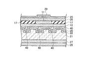
すなわち、本発明の第4の実施の形態に係る半導体発光素子は、図21に示すように、シリコン基板21と、シリコン基板21上に配置されるチタン層22と、チタン層22上に配置される金属層20とから構成されるシリコン基板構造と、金属層20上に配置される金属層12と、金属層12上に配置され,パターニングされた金属コンタクト層11および絶縁層17と、パターニングされた金属コンタクト層11および絶縁層17上に配置され,露出された表面にフロスト処理領域30(露出されたn型GaAs層25をフロスト処理して形成された領域)を有するエピタキシャル成長層26と、エピタキシャル成長層26上に配置され,パターニングされたn型GaAs層25と、n型GaAs層25上に配置され,同様にパターニングされた表面電極層29とから構成されるLED構造を備える。尚、シリコン基板構造において、シリコン基板21の裏面には、チタン層27と、裏面電極層28が配置される。また、エピタキシャル成長層26とn型GaAs層25の間には、後述する図22、図23に示すように、電流集中を防止するための阻止層31を配置しても良い。この場合の阻止層31の材料としては、GaAsを適用することができ、厚さは、例えば約500nm程度である。
That is, the semiconductor light emitting device according to the fourth embodiment of the present invention is disposed on the
本発明の第4の実施の形態に係る半導体発光素子においても、図21に示すように、金属層12を用いて、シリコン基板構造と、エピタキシャル成長層からなるLED構造を貼り付けることにより、反射率のよい金属反射層を形成することを可能にしている。金属反射層は、予め、LED構造側に配置された金属層12によって形成される。LEDからの放射光は、絶縁層17と金属層12との界面によってミラー面が形成されるため、当該ミラー面において反射される。金属コンタクト層11は、金属層12とエピタキシャル成長層26とのオーミックコンタクトを取るための層であるが、金属層12とエピタキシャル成長層26との界面に介在し、絶縁層17と同程度の厚さを有する。
Also in the semiconductor light emitting device according to the fourth embodiment of the present invention, as shown in FIG. 21, by using a
(平面パターン構造)
金属コンタクト層11のパターン幅が広い場合には、実質的な発光領域が制限されるため、面積効率が低下し発光効率が減少する。一方、金属コンタクト層11のパターン幅が狭い場合には、金属コンタクト層11の面積抵抗が増大し、LEDの順方向電圧Vfが上昇する。このため、最適なパターン幅WおよびパターンピッチD1が存在する。幾つかのパターン例では、六角形を基本とするハニカムパターン構造、或いは、円形ドット形状を基本構造とする円形ドットパターン構造が存在する。
(Plane pattern structure)
When the pattern width of the
本発明の第4の実施の形態に係る半導体発光素子およびその製造方法に適用されるLEDの模式的平面パターン構造は、例えば図14に示すように、六角形を基本構造とするハニカムパターン構造を有する。図14において、幅Wで示される形状部分が図13における例えばAuBe層あるいはAuBeとNiとの合金層などで形成される金属コンタクト層11のパターンを示し、幅D1を有する六角形パターンは、絶縁層17の部分に相当し、LEDからの放射光が導光する領域を表す。幅D1は、例えば約100μm程度であり、線幅Wは、約5μm〜約11μm程度である。
The schematic planar pattern structure of the LED applied to the semiconductor light emitting device and the manufacturing method thereof according to the fourth embodiment of the present invention is a honeycomb pattern structure having a hexagonal basic structure as shown in FIG. Have. 14, the shape portion indicated by the width W indicates the pattern of the
本発明の第4の実施の形態に係る半導体発光素子およびその製造方法に適用されるLEDの別の模式的平面パターン構造は、例えば図15に示すように、円形を基本とするドットパターン構造を有する。図15において、幅dで示される形状部分が図13における例えばAuBe層あるいはAuBeとNiとの合金層などで形成される金属コンタクト層11のパターンを示し、幅D2を有するパターンピッチで配置されている。図15において、幅d、パターンピッチD2を有する円形のパターン部分以外の領域が、絶縁層17の部分に相当し、LEDからの放射光が導光する領域を表す。パターンピッチD2は、例えば約100μm程度であり、幅dは、約5μm〜約11μm程度である。
Another schematic planar pattern structure of the LED applied to the semiconductor light emitting element and the manufacturing method thereof according to the fourth embodiment of the present invention is a dot pattern structure based on a circle as shown in FIG. Have. In FIG. 15, the shape portion indicated by the width d indicates the pattern of the
また、本発明の第4の実施の形態に係る半導体発光素子およびその製造方法に適用されるLEDの模式的平面パターン構造は、六角形ハニカムパターン、円形ドットパターンに限定されるものではなく、三角形パターン、矩形パターン、六角形パターン、八角形パターン、円形ドットパターンなどをランダムに配置するランダムパターンを適用することもできる。 In addition, the schematic planar pattern structure of the LED applied to the semiconductor light emitting device and the manufacturing method thereof according to the fourth embodiment of the present invention is not limited to the hexagonal honeycomb pattern and the circular dot pattern, but a triangle. A random pattern in which a pattern, a rectangular pattern, a hexagonal pattern, an octagonal pattern, a circular dot pattern, etc. are randomly arranged can also be applied.
本発明の第4の実施の形態に係る半導体発光素子に適用されるLEDの模式的平面パターン構造は、導光領域の面積を確保してLEDからの発光輝度を低下させず、かつをLEDの順方向電圧Vfが上昇しない程度の金属配線パターン幅を確保できればよい。 The schematic planar pattern structure of the LED applied to the semiconductor light emitting device according to the fourth embodiment of the present invention secures the area of the light guide region and does not decrease the light emission luminance from the LED. It is only necessary to secure a metal wiring pattern width that does not increase the forward voltage Vf.
(製造方法)
本発明の第4の実施の形態に係る半導体発光素子の製造方法を以下に説明する。
(Production method)
A method for manufacturing a semiconductor light emitting element according to the fourth embodiment of the present invention will be described below.
図12乃至図21は、本発明の第4の実施の形態に係る半導体発光素子の製造方法の一工程を説明する模式的断面構造を示す。 12 to 21 show a schematic cross-sectional structure for explaining one process of the method for manufacturing a semiconductor light emitting device according to the fourth embodiment of the present invention.
(a)まず、図12に示すように、貼付け用のシリコン基板構造、および図13に示すように、貼付け用のLED構造を準備する。 (A) First, as shown in FIG. 12, a silicon substrate structure for pasting and an LED structure for pasting as shown in FIG. 13 are prepared.
シリコン基板構造においては、シリコン基板21上にチタン層22およびAuなどからなる金属層20をスパッタリング法、真空蒸着法などを用いて順次形成する。
In the silicon substrate structure, a
LED構造においては、GaAs基板23上のAlInGaP層24、n型GaAs層25、エピタキシャル成長層26は、分子線エピタキシャル成長法(MBE:Molecular Beam Epitaxy)、MOCVD(Metal Organic Chemical Vapor Deposition)法などを用いて順次形成する。次に、エピタキシャル成長層26上にリフトオフ法を用いて、パターニングされた絶縁層17に対して、金属コンタクト層11および金属層12を形成する。
In the LED structure, the
(b)次に、図16に示すように、図12に示す貼付け用のシリコン基板構造、および図13に示す貼付け用のLED構造を貼り付ける。貼り付け工程においては、例えばプレス機を用いて、熱圧着温度として約340℃程度、熱圧着の圧力として約18MPa程度、熱圧着の時間として約10分程度の条件で実施する。 (B) Next, as shown in FIG. 16, the silicon substrate structure for pasting shown in FIG. 12 and the LED structure for pasting shown in FIG. 13 are pasted. In the attaching step, for example, using a press machine, the thermocompression bonding temperature is about 340 ° C., the thermocompression bonding pressure is about 18 MPa, and the thermocompression bonding time is about 10 minutes.
(c)次に、図17に示すように、シリコン基板21の裏面に対して、チタン層27およびAuなどからなる裏面電極層28をスパッタリング法、真空蒸着法などを用いて順次形成する。チタン層27をAu層とシリコン基板21との間に介在させない場合、オーミックコンタクトをとるためにシンタリングを実施するとシリコン基板21とAu層との接合部のAuがAuSiシリサイドとなり反射率が低下する。したがって、チタン層27は、シリコン基板21とAu層との接着用の金属である。AuSiシリサイド化を防ぐためには、バリアメタルとしてタングステン(W)が必要であり、そのときの構造として、基板側から、シリコン基板/Ti/W/Auで金属層を形成する必要がある。
(C) Next, as shown in FIG. 17, a
(d)次に、図18に示すように、裏面電極層28をレジストなどで保護した後、GaAs基板23をエッチングにより除去する。例えばアンモニア/過酸化水素水からなるエッチング液を用い、エッチング時間は、約65〜85分程度である。ここで、AllnGaP層24がエッチングストッパとして重要な働きをする。
(D) Next, as shown in FIG. 18, after the
(e)次に、図19に示すように、塩酸系のエッチング液を用いて、AllnGaP層24を除去する。エッチング時間は、例えば約1分半程度である。
(E) Next, as shown in FIG. 19, the
(f)次に、図20に示すように、表面電極層29をスパッタリング法、真空蒸着法などを用いて形成後、パターニングする。表面電極層29のパターンは金属コンタクト層11のパターンに略一致させている。表面電極層29の材料としては、例えばAu/AuGe−Ni合金/Auからなる積層構造を用いることができる。ここで、n型GaAs層25は表面電極層29の剥がれ防止機能を有する。
(F) Next, as shown in FIG. 20, the
(g)次に、図21に示すように、フロスト処理を実施して、表面電極層29の直下のn型GaAs層25以外のn型GaAs層25の除去を行う。フロスト処理の条件としては、例えば硝酸―硫酸系のエッチング液を約30℃〜50℃,時間約5sec〜15sec程度で行なうことができる。尚、フロスト処理の前処理としては、フッ酸の薄い液を用いてn型GaAs層25をエッチングして、表面に形成されたGaO2膜を除去することができる。エッチング時間としては、例えば約3分程度である。
(G) Next, as shown in FIG. 21, a frost process is performed to remove the n-
尚、チタン層22およびチタン層27の代りとして、例えばタングステン(W)バリアメタル、白金(Pt)バリアメタルなどを用いることもできる。
In place of the
以上の説明により、 図21に示すように、シリコン基板21を用いた本発明の第4の実施の形態に係る半導体発光素子が完成される。
As described above, as shown in FIG. 21, the semiconductor light emitting device according to the fourth embodiment of the present invention using the
(第4の実施の形態の変形例)
図22は、本発明の第4の実施の形態の変形例に係る半導体発光素子の製造方法の一工程を説明する模式的断面構造を示す。また、図23は、本発明の第4の実施の形態の別の変形例に係る半導体発光素子の製造方法の一工程を説明する模式的断面構造を示す。
(Modification of the fourth embodiment)
FIG. 22 shows a schematic cross-sectional structure for explaining one process of the method for manufacturing the semiconductor light emitting device according to the modification of the fourth embodiment of the present invention. FIG. 23 shows a schematic cross-sectional structure for explaining one step of a method for manufacturing a semiconductor light emitting element according to another modification of the fourth embodiment of the present invention.
本発明の第4の実施の形態の変形例に係る半導体発光素子は、図22に示すように、図12に示したシリコン基板構造と、図13に示したLED構造をウェハボンディング技術によって互いに貼り付けて形成する。 As shown in FIG. 22, the semiconductor light emitting device according to the modification of the fourth embodiment of the present invention is bonded to the silicon substrate structure shown in FIG. 12 and the LED structure shown in FIG. 13 by wafer bonding technology. Add and form.
すなわち、本発明の第4の実施の形態に係る半導体発光素子は、図21に示すように、GaAs基板15と、GaAs基板15上に配置される金属バッファ層(AuGe−Ni合金層)32と、金属バッファ層32上に配置される金属層(Au層)33とから構成されるGaAs基板構造と、金属層33上に配置される金属層12と、金属層12上に配置され,パターニングされた金属コンタクト層11および絶縁層17と、パターニングされた金属コンタクト層11および絶縁層17上に配置され,露出された表面にフロスト処理領域30(露出されたn型GaAs層25をフロスト処理して形成された領域)を有するエピタキシャル成長層26と、エピタキシャル成長層26上に配置され,パターニングされたn型GaAs層25と、n型GaAs層25上に配置され,同様にパターニングされた表面電極層29とから構成されるLED構造を備える。尚、GaAs基板構造において、GaAs基板15の裏面には、金属バッファ層(AuGe−Ni合金層)34と、裏面電極層35が配置される。また、エピタキシャル成長層26とn型GaAs層25の間には、図23に示すように、電流集中を防止するための阻止層31を配置しても良い。この場合の阻止層31の材料としては、GaAsを適用することができ、厚さは、例えば約500nm程度である。
That is, the semiconductor light emitting device according to the fourth embodiment of the present invention includes a
本発明の第4の実施の形態の変形例に係る半導体発光素子においても、図22に示すように、金属層12を用いて、GaAs基板構造と、エピタキシャル成長層からなるLED構造を貼り付けることにより、反射率のよい金属反射層を形成することを可能にしている。金属反射層は、予め、LED構造側に配置された金属層12によって形成される。LEDからの放射光は、絶縁層17と金属層12との界面によってミラー面が形成されるため、当該ミラー面において反射される。金属コンタクト層11は、金属層12とエピタキシャル成長層26とのオーミックコンタクトを取るための層であるが、金属層12とエピタキシャル成長層26との界面に介在し、絶縁層17と同程度の厚さを有する。
Also in the semiconductor light emitting device according to the modification of the fourth embodiment of the present invention, as shown in FIG. 22, by using a
図22および図23の構造において、GaAs基板15の裏面に形成される金属バッファ層34は、例えばAuGe−Ni合金層で形成され、厚さは約100nm程度である。また、裏面電極層35は、Au層で形成され、厚さは約500nm程度である。GaAs基板15の表面に形成される金属バッファ層32は、例えばAuGe−Ni合金層で形成され、厚さは約100nm程度である。さらに金属層33は、Au層で形成され、厚さは約1μm程度である。
22 and FIG. 23, the
図12乃至図21に示された本発明の第4の実施の形態に係る半導体発光素子の製造方法の各工程は、本発明の第4の実施の形態の変形例に係る半導体発光素子の製造方法においても同様であるため説明を省略する。 Each step of the method for manufacturing a semiconductor light emitting device according to the fourth embodiment of the present invention shown in FIGS. 12 to 21 includes the steps of manufacturing a semiconductor light emitting device according to a modification of the fourth embodiment of the present invention. Since the method is the same, the description thereof is omitted.
本発明の第4の実施の形態の変形例に係る半導体発光素子およびその製造方法に適用されるLEDの模式的平面パターン構造も、図14或いは図15と同様の構造を適用可能である。 The schematic planar pattern structure of the LED applied to the semiconductor light emitting device and the method for manufacturing the semiconductor light emitting device according to the modification of the fourth embodiment of the present invention can also be applied to the structure similar to FIG.
また、本発明の第4の実施の形態およびその変形例に係る半導体発光素子においても第2の実施の形態の変形例において説明した、絶縁層17と金属層12との間に、AgやAlなどからなる金属バッファ層18(図7参照)を形成することも有効である。AgやAlなどからなる金属バッファ層18を形成することことで、Auでは反射率の低い紫外線などの短波長の光を効率よく反射することができるからである。
Further, in the semiconductor light emitting device according to the fourth embodiment of the present invention and the modification thereof, Ag or Al is interposed between the insulating
本発明の第4の実施の形態およびその変形例に係る半導体発光素子およびその製造方法によれば、金属反射層と半導体層との間に透明な絶縁層17を介在させることにより、エピタキシャル成長層26と金属層12との接触を避け、光の吸収を防ぎ、反射率の良い金属反射層を形成することができるので、LEDの高輝度化を図ることができる。
According to the semiconductor light emitting device and the manufacturing method thereof according to the fourth embodiment of the present invention and the modification thereof, the
また、本発明の第4の実施の形態およびその変形例に係る半導体発光素子およびその製造方法によれば、絶縁層17と金属層12,20との間に、AgやAlなどからなる金属バッファ層を形成することで、Auでは反射率の低い紫外線などの短波長の光を効率よく反射することができ、LEDの高輝度化を図ることができる。
In addition, according to the semiconductor light emitting device and the manufacturing method thereof according to the fourth embodiment of the present invention and the modification thereof, the metal buffer made of Ag, Al, or the like between the insulating
また、本発明の第4の実施の形態およびその変形例に係る半導体発光素子およびその製造方法によれば、エピタキシャル成長層26と金属層12との接触を避け、エピタキシャル成長層26と金属反射層の界面において光が吸収されないため、LEDの高輝度化を図ることができる。
In addition, according to the semiconductor light emitting device and the manufacturing method thereof according to the fourth embodiment of the present invention and the modification thereof, the contact between the
本発明の第4の実施の形態およびその変形例に係る半導体発光素子およびその製造方法によれば、シリコン基板若しくはGaAs基板への光の吸収を防ぐために、反射層に金属を用いて光を全反射させ、シリコン基板若しくはGaAs基板への吸収を防ぎ、あらゆる角度の光を反射することが可能になるので、LEDを高輝度化することができる。 According to the semiconductor light emitting device and the method for manufacturing the same according to the fourth embodiment of the present invention and the modification thereof, the reflection layer is made of metal to prevent light from being absorbed into the silicon substrate or the GaAs substrate. The light can be reflected to prevent absorption into the silicon substrate or the GaAs substrate, and light at any angle can be reflected, so that the brightness of the LED can be increased.
[その他の実施の形態]
上記のように、本発明は第1乃至第4の実施の形態によって記載したが、この開示の一部をなす論述および図面はこの発明を限定するものであると理解すべきではない。この開示から当業者には様々な代替実施の形態、実施例および運用技術が明らかとなろう。
[Other embodiments]
As described above, the present invention has been described according to the first to fourth embodiments. However, it should not be understood that the description and drawings constituting a part of this disclosure limit the present invention. From this disclosure, various alternative embodiments, examples and operational techniques will be apparent to those skilled in the art.
本発明の第1乃至第4の実施の形態に係る半導体発光素子およびその製造方法においては、半導体基板として主としてシリコン基板、GaAs基板を例に説明したが、Ge、SiGe、SiC、GaN基板、或いはSiC上のGaNエピタキシャル基板なども充分に利用可能である。 In the semiconductor light emitting device and the manufacturing method thereof according to the first to fourth embodiments of the present invention, the silicon substrate and the GaAs substrate are mainly described as examples of the semiconductor substrate. However, the Ge, SiGe, SiC, GaN substrate, or A GaN epitaxial substrate on SiC or the like can be sufficiently used.
本発明の第1乃至第4の実施の形態に係る半導体発光素子として、主としてLEDを例に説明したが、レーザダイオード(LD:Laser Diode)を構成してもよく、その場合には、分布帰還型(DFB:Distributed Feedback)LD、分布ブラッグ反射型(DBR)LD、面発光LDなどを構成しても良い。 As the semiconductor light emitting device according to the first to fourth embodiments of the present invention, description has been made mainly using the LED as an example. However, a laser diode (LD) may be configured, and in that case, distributed feedback is possible. A DFB (Distributed Feedback) LD, a distributed Bragg reflection type (DBR) LD, a surface emitting LD, or the like may be configured.
このように、本発明はここでは記載していない様々な実施の形態などを含むことは勿論である。したがって、本発明の技術的範囲は上記の説明から妥当な特許請求の範囲に係る発明特定事項によってのみ定められるものである。 As described above, the present invention naturally includes various embodiments that are not described herein. Therefore, the technical scope of the present invention is defined only by the invention specifying matters according to the scope of claims reasonable from the above description.
本発明の実施の形態に係る半導体発光素子およびその製造方法は、GaAs基板、Si基板等の不透明基板を有するLED素子,LD素子等の半導体発光素子全般に利用可能である。 The semiconductor light emitting device and the manufacturing method thereof according to the embodiment of the present invention can be used for all semiconductor light emitting devices such as an LED device and an LD device having an opaque substrate such as a GaAs substrate or a Si substrate.
1、5、12、20、33…金属層(Au層)
2、4、18…金属バッファ層
3…p型GaAs層
6…n型GaAs層
7…ウィンドウ層
8…n型クラッド層
9…多重量子井戸(MQW)層
10…p型クラッド層
11…金属コンタクト層(AuBe−Ni合金)
15、23…GaAs基板
17…絶縁層
21…シリコン(Si)基板
22、27…チタン(Ti)層
24…AlInGaP層
25…n型GaAs層
26…エピタキシャル成長層
29…表面電極層
30…フロスト処理領域
31…阻止層
32、34…金属バッファ層(AuGe−Ni合金)
28、35…裏面電極層
40…エアギャップ(空隙)
1, 5, 12, 20, 33 ... metal layer (Au layer)
2, 4, 18 ...
DESCRIPTION OF
28, 35 ...
Claims (40)
前記GaAs基板構造上に配置され、第3金属層と、前記第3金属層上に配置される金属コンタクト層と、前記金属コンタクト層上に配置されるp型クラッド層と、前記p型クラッド層に配置される多重量子井戸層と、前記多重量子井戸層上に配置されるn型クラッド層と、前記n型クラッド層上に配置されるウィンドウ層を備える発光ダイオード構造とから構成され、
前記GaAs層の前記表面に配置された前記第1金属層および前記第3金属層を用いて、前記GaAs基板構造と、前記発光ダイオード構造を貼り付けるとともに、前記溝部の前記第1金属層と前記第3金属層との間にはエアギャップが存在することを特徴とする半導体発光素子。 A GaAs layer having a plurality of grooves formed on a surface; a first metal buffer layer disposed on the surface of the GaAs layer; a sidewall of the groove; and a bottom surface of the groove; and a first metal buffer layer disposed on the first metal buffer layer A GaAs substrate comprising a first metal layer, a second metal buffer layer disposed on the back surface of the GaAs layer, and a second metal layer disposed on the surface of the second metal buffer layer opposite to the GaAs layer. Structure and
A third metal layer disposed on the GaAs substrate structure; a metal contact layer disposed on the third metal layer; a p-type cladding layer disposed on the metal contact layer; and the p-type cladding layer A multi-quantum well layer disposed on the n-type cladding layer, and a light-emitting diode structure including a window layer disposed on the n-type cladding layer,
Using the first metal layer and the third metal layer disposed on the surface of the GaAs layer, the GaAs substrate structure and the light emitting diode structure are pasted, and the first metal layer in the groove and the A semiconductor light emitting device characterized in that an air gap exists between the third metal layer.
前記GaAs基板の前記表面,前記溝部の側壁および前記溝部の底面に配置される金属層と、
前記GaAs基板の前記表面上の前記金属層上に配置され,パターニングされた金属コンタクト層および絶縁層と、
パターニングされた前記金属コンタクト層および前記絶縁層上に配置されるp型クラッド層10と、
前記p型クラッド層上に配置される多重量子井戸層と、
前記多重量子井戸層上に配置されるn型クラッド層と、
前記n型クラッド層上に配置されるウィンドウ層を備える発光ダイオード構造とから構成され、
前記GaAs基板の前記表面上の前記金属層を用いて、前記GaAs基板と、前記発光ダイオード構造を貼り付けると共に、前記溝部の前記金属層と前記発光ダイオード構造との間にはエアギャップが存在することことを特徴とする半導体発光素子。 A GaAs substrate having a plurality of grooves formed on the surface;
A metal layer disposed on the surface of the GaAs substrate, side walls of the groove, and a bottom surface of the groove;
A patterned metal contact layer and insulating layer disposed on the metal layer on the surface of the GaAs substrate;
A p-type cladding layer 10 disposed on the patterned metal contact layer and the insulating layer;
A multiple quantum well layer disposed on the p-type cladding layer;
An n-type cladding layer disposed on the multiple quantum well layer;
A light emitting diode structure comprising a window layer disposed on the n-type cladding layer,
The metal layer on the surface of the GaAs substrate is used to attach the GaAs substrate and the light emitting diode structure, and an air gap exists between the metal layer in the groove and the light emitting diode structure. A semiconductor light emitting element characterized by the above.
当該GaAs基板構造上に配置され、第2金属層と、前記第2金属層上に配置されるp型クラッド層と、前記p型クラッド層上に配置される多重量子井戸層と、前記多重量子井戸層上に配置されるn型クラッド層と、前記n型クラッド層上に配置されるウィンドウ層を備える発光ダイオード構造とから構成され、
前記GaAs基板の前記表面上の前記第1金属層および前記第2金属層を用いて、前記GaAs基板と、前記発光ダイオード構造を貼り付けると共に、前記溝部の前記第1金属層と前記発光ダイオード構造との間にはエアギャップが存在することを特徴とする半導体発光素子。 A GaAs substrate structure comprising: a GaAs substrate having a plurality of grooves formed on a surface; and a first metal layer disposed on the surface of the GaAs substrate, a sidewall of the groove, and a bottom surface of the groove;
A second metal layer disposed on the GaAs substrate structure; a p-type cladding layer disposed on the second metal layer; a multiple quantum well layer disposed on the p-type cladding layer; and the multiple quantum An n-type cladding layer disposed on the well layer, and a light emitting diode structure including a window layer disposed on the n-type cladding layer,
The first metal layer and the second metal layer on the surface of the GaAs substrate are used to attach the GaAs substrate and the light emitting diode structure, and the first metal layer and the light emitting diode structure in the groove portion. A semiconductor light emitting device characterized in that an air gap exists between the two.
前記第1金属層上に配置される第2金属層と、前記第2金属層上に配置され,パターニングされた金属コンタクト層および絶縁層と、パターニングされた前記金属コンタクト層および前記絶縁層上に配置され,露出された表面にフロスト処理領域を有するエピタキシャル成長層と、前記エピタキシャル成長層上に配置され,パターニングされたn型GaAs層と、前記n型GaAs層上に配置され,パターニングされた表面電極層とから構成されるLED構造とを備え、
前記シリコン基板の前記表面上の前記第1金属層および前記第2金属層を用いて、前記シリコン基板構造と、前記発光ダイオード構造を貼り付けると共に、前記溝部の前記第1金属層と前記LED構造との間にはエアギャップが存在することを特徴とする半導体発光素子。 A silicon substrate having a plurality of grooves formed on the surface; a titanium layer disposed on the surface of the silicon substrate; a sidewall of the groove; and a bottom surface of the groove; a first metal layer disposed on the titanium layer; A silicon substrate structure comprising:
A second metal layer disposed on the first metal layer; a patterned metal contact layer and insulating layer disposed on the second metal layer; and the patterned metal contact layer and insulating layer. An epitaxially grown layer having a frosted region disposed on the exposed surface, an n-type GaAs layer disposed on the epitaxially grown layer and patterned, and a surface electrode layer disposed on the n-type GaAs layer and patterned An LED structure composed of
Using the first metal layer and the second metal layer on the surface of the silicon substrate, the silicon substrate structure and the light emitting diode structure are pasted, and the first metal layer and the LED structure in the groove portion A semiconductor light emitting device characterized in that an air gap exists between the two.
前記第1金属層上に配置される第2金属層と、前記第2金属層上に配置され,パターニングされた金属コンタクト層および絶縁層と、パターニングされた前記金属コンタクト層および前記絶縁層上に配置され,露出された表面にフロスト処理領域を有するエピタキシャル成長層と、前記エピタキシャル成長層上に配置され,パターニングされたn型GaAs層と、前記n型GaAs層上に配置され,パターニングされた表面電極層とから構成されるLED構造を備え、
前記GaAs基板の前記表面上の前記第1金属層および前記第2金属層を用いて、前記GaAs基板構造と、前記発光ダイオード構造を貼り付けると共に、前記溝部の前記第1金属層上に配置される第2金属層と前記LED構造との間にはエアギャップが存在することを特徴とする半導体発光素子。 A GaAs substrate having a plurality of grooves formed on the surface; a metal buffer layer disposed on the surface of the GaAs substrate; a sidewall of the groove; and a bottom surface of the groove; a first metal disposed on the metal buffer layer A GaAs substrate structure composed of layers;
A second metal layer disposed on the first metal layer; a patterned metal contact layer and insulating layer disposed on the second metal layer; and the patterned metal contact layer and insulating layer. An epitaxially grown layer having a frosted region disposed on the exposed surface, an n-type GaAs layer disposed on the epitaxially grown layer and patterned, and a surface electrode layer disposed on the n-type GaAs layer and patterned LED structure composed of
The first metal layer and the second metal layer on the surface of the GaAs substrate are used to attach the GaAs substrate structure and the light emitting diode structure, and are disposed on the first metal layer in the groove. An air gap exists between the second metal layer and the LED structure.
前記半導体基板構造においては、半導体基板の表面に複数の溝部を形成した後、前記半導体基板上に第1金属層を形成する工程と、
前記発光ダイオード構造においては、GaAs基板上にAlInGaP層、n型GaAs層、エピタキシャル成長層を順次形成する工程と、
前記エピタキシャル成長層上に、パターニングされた絶縁層に対して、金属コンタクト層および第2金属層を形成する工程と、
前記半導体基板の前記表面上の前記第1金属層を用いて、前記半導体基板と、前記貼付け用のLED構造を熱圧着により貼り付けると共に、前記溝部の前記第1金属層と前記LED構造との間にはエアギャップを形成する工程と、
前記GaAs基板をエッチングにより除去する工程と、
前記AllnGaP層を除去する工程と、
表面電極層をパターン形成する工程と、
フロスト処理を実施して、前記表面電極層の直下の前記n型GaAs層以外の前記n型GaAs層の除去を行う工程と
を有することを特徴とする半導体発光素子の製造方法。 Preparing a semiconductor substrate structure for pasting and a light emitting diode structure for pasting;
In the semiconductor substrate structure, after forming a plurality of grooves on the surface of the semiconductor substrate, forming a first metal layer on the semiconductor substrate;
In the light emitting diode structure, an AlInGaP layer, an n-type GaAs layer, and an epitaxial growth layer are sequentially formed on a GaAs substrate;
Forming a metal contact layer and a second metal layer on the epitaxially grown layer with respect to the patterned insulating layer;
Using the first metal layer on the surface of the semiconductor substrate, the semiconductor substrate and the LED structure for pasting are pasted by thermocompression bonding, and the first metal layer and the LED structure in the groove are A process of forming an air gap between them,
Removing the GaAs substrate by etching;
Removing the AllnGaP layer;
Patterning the surface electrode layer;
And a step of removing the n-type GaAs layer other than the n-type GaAs layer immediately below the surface electrode layer by performing a frost treatment.
Priority Applications (6)
| Application Number | Priority Date | Filing Date | Title |
|---|---|---|---|
| JP2007156381A JP5123573B2 (en) | 2007-06-13 | 2007-06-13 | Semiconductor light emitting device and manufacturing method thereof |
| PCT/JP2008/060476 WO2008152988A1 (en) | 2007-06-13 | 2008-06-06 | Semiconductor light emitting element and method for manufacturing the same |
| EP08765289.7A EP2157623B1 (en) | 2007-06-13 | 2008-06-06 | Semiconductor light emitting element and method for manufacturing the same |
| CN2008800199380A CN101681970B (en) | 2007-06-13 | 2008-06-06 | Semiconductor light emitting element and method for manufacturing the same |
| KR1020107000402A KR101473038B1 (en) | 2007-06-13 | 2008-06-06 | Semiconductor light emitting element and method for manufacturing the same |
| US12/452,027 US8039864B2 (en) | 2007-06-13 | 2008-06-06 | Semiconductor light emitting device and fabrication method for the same |
Applications Claiming Priority (1)
| Application Number | Priority Date | Filing Date | Title |
|---|---|---|---|
| JP2007156381A JP5123573B2 (en) | 2007-06-13 | 2007-06-13 | Semiconductor light emitting device and manufacturing method thereof |
Related Child Applications (1)
| Application Number | Title | Priority Date | Filing Date |
|---|---|---|---|
| JP2012233568A Division JP5396526B2 (en) | 2012-10-23 | 2012-10-23 | Semiconductor light emitting device |
Publications (2)
| Publication Number | Publication Date |
|---|---|
| JP2008311352A JP2008311352A (en) | 2008-12-25 |
| JP5123573B2 true JP5123573B2 (en) | 2013-01-23 |
Family
ID=40129593
Family Applications (1)
| Application Number | Title | Priority Date | Filing Date |
|---|---|---|---|
| JP2007156381A Expired - Fee Related JP5123573B2 (en) | 2007-06-13 | 2007-06-13 | Semiconductor light emitting device and manufacturing method thereof |
Country Status (6)
| Country | Link |
|---|---|
| US (1) | US8039864B2 (en) |
| EP (1) | EP2157623B1 (en) |
| JP (1) | JP5123573B2 (en) |
| KR (1) | KR101473038B1 (en) |
| CN (1) | CN101681970B (en) |
| WO (1) | WO2008152988A1 (en) |
Families Citing this family (28)
| Publication number | Priority date | Publication date | Assignee | Title |
|---|---|---|---|---|
| KR100599012B1 (en) * | 2005-06-29 | 2006-07-12 | 서울옵토디바이스주식회사 | Light emitting diode having a thermal conductive substrate and method of fabricating the same |
| JP5346443B2 (en) | 2007-04-16 | 2013-11-20 | ローム株式会社 | Semiconductor light emitting device and manufacturing method thereof |
| US8299455B2 (en) * | 2007-10-15 | 2012-10-30 | International Business Machines Corporation | Semiconductor structures having improved contact resistance |
| JP5651288B2 (en) * | 2008-03-25 | 2015-01-07 | 株式会社東芝 | Semiconductor light emitting device and manufacturing method thereof |
| JP2010067890A (en) * | 2008-09-12 | 2010-03-25 | Hitachi Cable Ltd | Light-emitting element |
| JP2010251531A (en) * | 2009-04-16 | 2010-11-04 | Rohm Co Ltd | Semiconductor light-emitting element |
| CN101840966B (en) * | 2009-05-08 | 2013-07-03 | 晶能光电(江西)有限公司 | Semiconductor light emitting device and method for preparing light emitting diode |
| KR101014013B1 (en) * | 2009-10-15 | 2011-02-10 | 엘지이노텍 주식회사 | Semiconductor light emitting device and fabrication method thereof |
| KR101081193B1 (en) | 2009-10-15 | 2011-11-07 | 엘지이노텍 주식회사 | Semiconductor light emitting device and fabrication method thereof |
| KR101072034B1 (en) * | 2009-10-15 | 2011-10-10 | 엘지이노텍 주식회사 | Semiconductor light emitting device and fabrication method thereof |
| KR101728545B1 (en) * | 2010-04-23 | 2017-04-19 | 엘지이노텍 주식회사 | Light emitting device, method for fabricating the light emitting device and light emitting device package |
| CN102376830B (en) * | 2010-08-19 | 2015-07-08 | 展晶科技(深圳)有限公司 | Light emitting diode and manufacturing method thereof |
| KR101138951B1 (en) * | 2010-08-23 | 2012-04-25 | 서울옵토디바이스주식회사 | Light emitting diode |
| US8154034B1 (en) | 2010-11-23 | 2012-04-10 | Invenlux Limited | Method for fabricating vertical light emitting devices and substrate assembly for the same |
| TWI419367B (en) * | 2010-12-02 | 2013-12-11 | Epistar Corp | Optoelectronic device and method for manufacturing the same |
| TWI546979B (en) * | 2012-03-05 | 2016-08-21 | 晶元光電股份有限公司 | Lighting emitting device with aligned-bonding and the manufacturing method thereof |
| KR20140018534A (en) * | 2012-08-02 | 2014-02-13 | 엘지이노텍 주식회사 | Light emitting device |
| JP6068091B2 (en) * | 2012-10-24 | 2017-01-25 | スタンレー電気株式会社 | Light emitting element |
| TWI563686B (en) * | 2012-12-21 | 2016-12-21 | Hon Hai Prec Ind Co Ltd | Led chip and method manufacturing the same |
| TWI644451B (en) * | 2013-07-10 | 2018-12-11 | 晶元光電股份有限公司 | Light-emitting element |
| CN103594579B (en) * | 2013-11-06 | 2016-04-13 | 南昌黄绿照明有限公司 | A kind of epitaxial structure of iii-nitride light emitting devices |
| DE102014108301A1 (en) * | 2014-06-12 | 2015-12-17 | Osram Opto Semiconductors Gmbh | Semiconductor chip and method for producing a semiconductor chip |
| KR20160037060A (en) * | 2014-09-26 | 2016-04-05 | 서울바이오시스 주식회사 | Light emitting device and method for fabricating the same |
| US9773906B2 (en) * | 2015-04-28 | 2017-09-26 | Samsung Electronics Co., Ltd. | Relaxed semiconductor layers with reduced defects and methods of forming the same |
| KR102336432B1 (en) * | 2015-09-01 | 2021-12-07 | 쑤저우 레킨 세미컨덕터 컴퍼니 리미티드 | Light emitting device and light emitting device package |
| KR102573271B1 (en) * | 2018-04-27 | 2023-08-31 | 삼성전자주식회사 | Semiconductor light emitting device |
| US20230106189A1 (en) * | 2021-10-01 | 2023-04-06 | Lawrence Livermore National Security, Llc | Patterning of diode/substrate interface to reduce thermal lensing |
| CN116364825A (en) * | 2023-06-01 | 2023-06-30 | 江西兆驰半导体有限公司 | Composite buffer layer, preparation method thereof, epitaxial wafer and light-emitting diode |
Family Cites Families (15)
| Publication number | Priority date | Publication date | Assignee | Title |
|---|---|---|---|---|
| US5376580A (en) | 1993-03-19 | 1994-12-27 | Hewlett-Packard Company | Wafer bonding of light emitting diode layers |
| US5565694A (en) * | 1995-07-10 | 1996-10-15 | Huang; Kuo-Hsin | Light emitting diode with current blocking layer |
| US5759753A (en) * | 1995-07-19 | 1998-06-02 | Matsushita Electric Industrial Co., Ltd. | Piezoelectric device and method of manufacturing the same |
| JP2907170B2 (en) * | 1996-12-28 | 1999-06-21 | サンケン電気株式会社 | Semiconductor light emitting device |
| JPH11103090A (en) * | 1997-09-29 | 1999-04-13 | Hitachi Cable Ltd | Light-emitting diode |
| US6406636B1 (en) * | 1999-06-02 | 2002-06-18 | Megasense, Inc. | Methods for wafer to wafer bonding using microstructures |
| US20020017652A1 (en) * | 2000-08-08 | 2002-02-14 | Stefan Illek | Semiconductor chip for optoelectronics |
| JP4004378B2 (en) * | 2002-10-24 | 2007-11-07 | ローム株式会社 | Semiconductor light emitting device |
| FR2857502B1 (en) * | 2003-07-10 | 2006-02-24 | Soitec Silicon On Insulator | SUBSTRATES FOR CONSTRAINTS SYSTEMS |
| JP4114566B2 (en) * | 2003-07-24 | 2008-07-09 | 信越半導体株式会社 | Semiconductor bonded assembly and method for manufacturing the same, light emitting device and method for manufacturing the same |
| TWI223460B (en) * | 2003-09-23 | 2004-11-01 | United Epitaxy Co Ltd | Light emitting diodes in series connection and method of making the same |
| JP2005223207A (en) | 2004-02-06 | 2005-08-18 | Sharp Corp | Semiconductor light-emitting element and its manufacturing method |
| TWI244220B (en) * | 2004-02-20 | 2005-11-21 | Epistar Corp | Organic binding light-emitting device with vertical structure |
| JP4978877B2 (en) * | 2004-06-10 | 2012-07-18 | 信越半導体株式会社 | Light emitting device manufacturing method and light emitting device |
| US7705465B2 (en) * | 2005-04-01 | 2010-04-27 | Panasonic Corporation | Surface-mount type optical semiconductor device and method for manufacturing the same |
-
2007
- 2007-06-13 JP JP2007156381A patent/JP5123573B2/en not_active Expired - Fee Related
-
2008
- 2008-06-06 KR KR1020107000402A patent/KR101473038B1/en active IP Right Grant
- 2008-06-06 WO PCT/JP2008/060476 patent/WO2008152988A1/en active Application Filing
- 2008-06-06 EP EP08765289.7A patent/EP2157623B1/en not_active Not-in-force
- 2008-06-06 US US12/452,027 patent/US8039864B2/en active Active
- 2008-06-06 CN CN2008800199380A patent/CN101681970B/en not_active Expired - Fee Related
Also Published As
| Publication number | Publication date |
|---|---|
| EP2157623A4 (en) | 2013-12-25 |
| US20100133505A1 (en) | 2010-06-03 |
| KR101473038B1 (en) | 2014-12-15 |
| EP2157623B1 (en) | 2017-01-18 |
| EP2157623A1 (en) | 2010-02-24 |
| JP2008311352A (en) | 2008-12-25 |
| CN101681970A (en) | 2010-03-24 |
| US8039864B2 (en) | 2011-10-18 |
| WO2008152988A1 (en) | 2008-12-18 |
| KR20100020515A (en) | 2010-02-22 |
| CN101681970B (en) | 2011-08-24 |
Similar Documents
| Publication | Publication Date | Title |
|---|---|---|
| JP5123573B2 (en) | Semiconductor light emitting device and manufacturing method thereof | |
| JP5346443B2 (en) | Semiconductor light emitting device and manufacturing method thereof | |
| JP2002217450A (en) | Semiconductor light-emitting device and method of manufacturing the same | |
| JP2010251531A (en) | Semiconductor light-emitting element | |
| JP5584331B2 (en) | Semiconductor light emitting device | |
| JP5396526B2 (en) | Semiconductor light emitting device | |
| JP5981493B2 (en) | Semiconductor light emitting device | |
| KR100564303B1 (en) | Light emitting diode and fabrication method thereof | |
| JP2018050070A (en) | Semiconductor light emitting element | |
| JP5690395B2 (en) | Manufacturing method of semiconductor light emitting device |
Legal Events
| Date | Code | Title | Description |
|---|---|---|---|
| A621 | Written request for application examination |
Free format text: JAPANESE INTERMEDIATE CODE: A621 Effective date: 20100610 |
|
| TRDD | Decision of grant or rejection written | ||
| A01 | Written decision to grant a patent or to grant a registration (utility model) |
Free format text: JAPANESE INTERMEDIATE CODE: A01 Effective date: 20121002 |
|
| A01 | Written decision to grant a patent or to grant a registration (utility model) |
Free format text: JAPANESE INTERMEDIATE CODE: A01 |
|
| A61 | First payment of annual fees (during grant procedure) |
Free format text: JAPANESE INTERMEDIATE CODE: A61 Effective date: 20121026 |
|
| FPAY | Renewal fee payment (event date is renewal date of database) |
Free format text: PAYMENT UNTIL: 20151102 Year of fee payment: 3 |
|
| R150 | Certificate of patent or registration of utility model |
Free format text: JAPANESE INTERMEDIATE CODE: R150 Ref document number: 5123573 Country of ref document: JP Free format text: JAPANESE INTERMEDIATE CODE: R150 |
|
| R250 | Receipt of annual fees |
Free format text: JAPANESE INTERMEDIATE CODE: R250 |
|
| LAPS | Cancellation because of no payment of annual fees |