JP5119826B2 - Compensation voltage circuit and temperature compensated piezoelectric oscillator - Google Patents
Compensation voltage circuit and temperature compensated piezoelectric oscillator Download PDFInfo
- Publication number
- JP5119826B2 JP5119826B2 JP2007246667A JP2007246667A JP5119826B2 JP 5119826 B2 JP5119826 B2 JP 5119826B2 JP 2007246667 A JP2007246667 A JP 2007246667A JP 2007246667 A JP2007246667 A JP 2007246667A JP 5119826 B2 JP5119826 B2 JP 5119826B2
- Authority
- JP
- Japan
- Prior art keywords
- compensation voltage
- voltage
- temperature
- terminal
- transistor
- Prior art date
- Legal status (The legal status is an assumption and is not a legal conclusion. Google has not performed a legal analysis and makes no representation as to the accuracy of the status listed.)
- Active
Links
Images


Description
本発明は、補償電圧回路及び温度補償型圧電発振器に関し、補償電圧回路の出力電圧を温度変化に対し滑らかに変化するようにし、発振周波数に生じる急激な周波数変動(ディップ)を抑圧した温度補償型圧電発振器に関する。 The present invention relates to a compensation voltage circuit and a temperature compensation type piezoelectric oscillator, and relates to a temperature compensation type in which an output voltage of the compensation voltage circuit changes smoothly with respect to a temperature change and a rapid frequency fluctuation (dip) occurring in an oscillation frequency is suppressed. The present invention relates to a piezoelectric oscillator.
近年、圧電発振器は周波数安定度、小型軽量、低価格等により携帯電話等の通信機器から水晶時計のような民生機器まで、多くの分野で用いられている。中でも圧電振動子の周波数温度特性を補償した温度補償型圧電発振器(TCXO)は、周波数安定度を必要とする携帯電話等に広く用いられている。
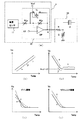
特許文献1には、関数発生回路を備えた温度補償水晶発振器が開示されている。図10は、その温度補償水晶発振器の機能ブロック図であり、定電圧回路32と、温度センサ回路33と、水晶振動子の温度特性を補償するため制御電圧Vcを生成する制御回路34と、電圧制御水晶発振器(VCXO)35と、制御回路34が出力する制御電圧Vcに対し、VCXO35が出力する発振周波数を最適化するため、制御電圧Vcの温度特性を補償する温度補償パラメータを記憶するROM/RAM回路36と、を備えている。
制御回路34は、MAX回路34aとMIN回路34bとからなる。定電圧回路32と温度センサ回路33とによって生成される制御電圧y1、制御電圧y2及び制御電圧y3を、制御回路34aに入力すると、その内の最大電圧値を選択して制御電圧y6として出力する。また、同様に生成される制御電圧y4及び制御電圧y5並びにMAX回路34aからの制御電圧y6を、制御回路34bに入力すると、その内の最小電圧値を選択して制御電圧y7を出力する。この制御電圧y7が温度補償用の制御電圧Vcとなる。
In recent years, piezoelectric oscillators are used in many fields from communication devices such as mobile phones to consumer devices such as quartz watches because of their frequency stability, small size and light weight, and low price. In particular, a temperature compensated piezoelectric oscillator (TCXO) that compensates for the frequency temperature characteristics of a piezoelectric vibrator is widely used in mobile phones and the like that require frequency stability.
The
図11は制御電圧Vcの詳細を示す図である。図11は、第1の温度領域(T0≦Ta≦T1)における制御電圧y1、第2の温度領域(T1≦Ta≦T2)における制御電圧y2、第3の温度領域(T2≦Ta≦T3)における制御電圧y3、第4の温度領域(T3≦Ta≦T4)における制御電圧y4、第5の温度領域(T4≦Ta≦T5)における制御電圧y5、を夫々示す折れ線状の直線群を示し、制御電圧Vcは太実線で表す折れ線となる。この制御電圧Vcを電圧制御水晶発振器35に加えると、温度補償型水晶発振器が構成される。なお、ROM/RAM回路36は、図示していないが、直列に接続された4個のフリップフロップからなるシリアルデータ入力部としてのRAMデータ入力回路と、該RAMデータ入力回路の出力データを受け、1ビット毎に記憶する4個のPROM回路と、制御信号(SEL、W/R、DATA等)とを有している。 FIG. 11 is a diagram showing details of the control voltage Vc. FIG. 11 shows the control voltage y1 in the first temperature region (T0 ≦ Ta ≦ T1), the control voltage y2 in the second temperature region (T1 ≦ Ta ≦ T2), and the third temperature region (T2 ≦ Ta ≦ T3). , The control voltage y3 in the fourth temperature region (T3 ≦ Ta ≦ T4), and the control voltage y5 in the fifth temperature region (T4 ≦ Ta ≦ T5), respectively. The control voltage Vc is a broken line represented by a thick solid line. When this control voltage Vc is applied to the voltage controlled crystal oscillator 35, a temperature compensated crystal oscillator is configured. Although not shown, the ROM / RAM circuit 36 receives a RAM data input circuit as a serial data input unit composed of four flip-flops connected in series, and output data of the RAM data input circuit. It has four PROM circuits for storing each bit and control signals (SEL, W / R, DATA, etc.).
特許文献2には、温度補償電圧を所定の電圧にクリップするクリップ電圧発生回路を備えた温度補償型圧電発振器50が開示されている。図12は温度補償型圧電発振器50の回路構成を示す図であり、発振回路52と、温度変化による圧電振動子の周波数変動を補償する周波数温度補償回路51と、から構成される。周波数温度補償回路51は、温度検出部53と、この温度検出部53の変化したパラメータに基づいて電圧を発生する温度補償電圧発生回路52と、この温度補償電圧発生回路52が出力する温度補償電圧(VH、VL)と、基準電圧(Vref)との電位差に基づいて容量が変化するMOS容量素子MH、MLと、温度補償電圧を所定の電圧にクリップするクリップ電圧発生回路55と、から構成される。
図13は補償電圧の温度特性を示す図である。温度が低温から高温に上昇する場合を考える。低温補償電圧VLは、温度が低温(−40℃)のときVLと基準電圧Vrefとの交点Rにあり、そのときの低温用MOS容量素子MLの端子間電圧は0Vである。温度が上昇するとVLは直線的に低下し、それに伴ってMLの端子間電圧が大きくなりMLの容量が増加する。そして、常温(+25℃)付近になると、クリップ電圧発生回路55のクリップ電圧Vcl2より、VLが低くなるように回路設定することで、+25℃付近でのクリップ電圧発生回路55のダイオードD2が順バイアスとなり、接続点Pはクリップ電圧Vcl2の電圧となる。更に温度が上昇するとVLは更に低下するが、クリップ電圧Vcl2によってクリップされているので、図13に示すごとく一定となる。
FIG. 13 is a diagram showing temperature characteristics of the compensation voltage. Consider the case where the temperature rises from low to high. The low-temperature compensation voltage VL is at the intersection R between the VL and the reference voltage Vref when the temperature is low (−40 ° C.), and the voltage between the terminals of the low-temperature MOS capacitor ML at that time is 0V. When the temperature rises, VL decreases linearly, and accordingly, the ML terminal voltage increases and the ML capacity increases. Then, by setting the circuit so that VL becomes lower than the clip voltage Vcl2 of the clip
次に温度が高温から低温に下降する場合を考える。高温補償電圧VHは、VHが高温(+90℃)のときVHと基準電圧Vrefとの交点Sにあり、そのときの高温用MOS容量素子MHの端子間電圧は0Vであるので、MHはC―V特性の立ち上がりの範囲の容量となる。温度が低下するとVHは直線的に低下し、それに伴ってMHの順バイアスの電位差が大きくなり、容量が減少する。そして、+25℃付近になると、クリップ電圧発生回路55のクリップ電圧Vcl2よりVHが低くなるよう回路設定することで、クリップ電圧発生回路55のダイオードD1が順バイアスとなり、接続点Qはクリップ電圧Vcl2の電圧となる。折れ線RPQSが補償電圧となる。この補償電圧が低、高温用MOS容量素子ML、MH及び容量からなる補償回路に印加されて、温度補償型圧電発振器が構成される。
しかしながら、特許文献1に開示された関数発生回路、水晶発振装置及び水晶発振装置の調整方法は、IC回路の半導体素子数が極めて多くなり、コストの上昇、歩留まりの低下を来すという問題があった。更に、関数発生回路から出力される制御電圧は折れ線状であり、直線と直線とのつなぎ目では電圧の変化は急激となり、所望の制御電圧(補償電圧)と、生成される制御電圧との誤差が大きくなるという問題があった。また、温度変化に対し制御電圧が急激に変化すると、水晶発振装置の出力周波数に周波数ディップが発生し、この水晶発振装置を搭載する機器に悪影響を及ぼす虞があるという問題があった。
また、特許文献2に開示された補償電圧も3本の直線からなる折れ線であり、直線と直線とのつなぎ目では電圧の変化は急激であり、所望の補償電圧と生成される補償電圧の誤差が大きいという問題と、上記の折れ線状の補償電圧を用いた温度補償型圧電発振器の出力には、周波数ディップ(周波数が急激に変化する現象)が発生するという問題があった。
本発明は上記問題を解決するためになされたもので、簡単な回路構成で直線と直線とのつなぎ目を滑らかにし、温度補償精度を改善した補償電圧回路及び温度補償型圧電発振器を提供することにある。
However, the function generation circuit, the crystal oscillation device, and the method for adjusting the crystal oscillation device disclosed in
Further, the compensation voltage disclosed in
The present invention has been made to solve the above-described problem, and provides a compensation voltage circuit and a temperature compensation type piezoelectric oscillator in which a straight line and a straight line are smoothed with a simple circuit configuration and temperature compensation accuracy is improved. is there.
上記目的を達成するため、本発明の補償電圧回路は、周囲の温度を感知する温度センサと、該温度センサの温度検知結果に応じて補償電圧を発生する補償電圧発生部と、を備えた補償電圧回路であって、補償電圧発生部は、温度センサの出力電圧を増幅する演算増幅器と、トランジスタと、を備え、トランジスタの第1端子と第2端子とがそれぞれ、演算増幅器の反転入力端子と出力端子とに接続されたものであることを特徴とする。
このように補償電圧回路を構成すると、温度に対する補償電圧特性は、直線と直線との交点近傍が滑らかな曲線で連なる補償電圧特性となり、この補償電圧回路を温度補償型圧電発振器に適用すると、周波数の補償精度も改良され、周波数ディップも抑制できるという効果がある。
To achieve the above object, a compensation voltage circuit according to the present invention comprises a temperature sensor that senses the ambient temperature, and a compensation voltage generator that generates a compensation voltage according to the temperature detection result of the temperature sensor. The compensation voltage generator includes an operational amplifier that amplifies the output voltage of the temperature sensor and a transistor, and a first terminal and a second terminal of the transistor are respectively an inverting input terminal of the operational amplifier. It is connected to an output terminal.
When the compensation voltage circuit is configured as described above, the compensation voltage characteristic with respect to the temperature becomes a compensation voltage characteristic in which the vicinity of the intersection of the straight line is connected by a smooth curve. When this compensation voltage circuit is applied to a temperature compensated piezoelectric oscillator, the frequency The compensation accuracy is improved, and the frequency dip can be suppressed.
また本発明の補償電圧回路は、温度センサと演算増幅器との間にゲイン調整を行うゲイン調整用増幅器を設けるようにした。
このように補償電圧回路を構成すると、ゲイン調整用増幅器のゲインを変えることにより補償電圧特性の傾斜部を上下することが可能となり、傾斜部の勾配を変える演算増幅器のゲイン調整と相まって補償電圧特性を所望の特性に近似することができるという効果がある。
また本発明の補償電圧回路は、温度センサとトランジスタのゲート(第3端子)との間にゲイン調整を行うゲイン調整用増幅器を設けるようにした。
このように補償電圧回路を構成すると、ゲイン調整用増幅器のゲインを変えることにより、特に補償電圧特性の平坦部の特性を、温度に対し単調増加、平坦、単調減少と変えることが可能となり、補償電圧特性の近似の精度を向上させることができるという効果がある。
In the compensation voltage circuit of the present invention, a gain adjusting amplifier for adjusting the gain is provided between the temperature sensor and the operational amplifier.
When the compensation voltage circuit is configured in this way, it is possible to raise or lower the slope of the compensation voltage characteristic by changing the gain of the gain adjustment amplifier, and in combination with the gain adjustment of the operational amplifier that changes the slope of the slope, the compensation voltage characteristic Can be approximated to a desired characteristic.
In the compensation voltage circuit of the present invention, a gain adjusting amplifier for adjusting the gain is provided between the temperature sensor and the gate (third terminal) of the transistor.
When the compensation voltage circuit is configured in this way, by changing the gain of the gain adjustment amplifier, it is possible to change the characteristic of the flat part of the compensation voltage characteristic, in particular, monotonically increasing, flat, and monotonically decreasing with respect to temperature. There is an effect that the accuracy of approximation of the voltage characteristic can be improved.
また本発明の補償電圧回路は、トランジスタは複数のトランジスタを並列接続したものであって、複数のトランジスタのそれぞれの第1端子が演算増幅器の反転入力端子に接続され、複数のトランジスタのそれぞれの第2端子が演算増幅器の出力端子に接続されたものであることを特徴とする。
このように補償電圧回路を構成すると、複数のゲイン調整用増幅器のゲインを夫々調整することにより補償電圧特性の曲線部をより微細に調整することが可能となり、演算増幅器のゲイン調整と相まって、補償電圧特性を所望の特性に近づけることができるという効果がある。
また本発明の補償電圧回路は、補償電圧発生部は、さらにダイオードを備え、演算増幅器の出力ラインにダイオードのカソード端子を接続し、ダイオードのアノード端子に基準電圧に印加したことを特徴とする。
このように補償電圧回路を構成すると、補償電圧回路の出力電圧を基準電圧で決まるクリップ電圧に保持することができるという利点がある。
In the compensation voltage circuit according to the present invention, the transistor includes a plurality of transistors connected in parallel, each of the plurality of transistors having a first terminal connected to an inverting input terminal of the operational amplifier, and each of the plurality of transistors having a first terminal. Two terminals are connected to an output terminal of an operational amplifier.
By configuring the compensation voltage circuit in this way, it is possible to finely adjust the curve portion of the compensation voltage characteristic by adjusting the gain of each of the plurality of gain adjustment amplifiers. The voltage characteristic can be brought close to a desired characteristic.
In the compensation voltage circuit of the present invention, the compensation voltage generator further includes a diode, the cathode terminal of the diode is connected to the output line of the operational amplifier, and the reference voltage is applied to the anode terminal of the diode.
By configuring the compensation voltage circuit in this way, there is an advantage that the output voltage of the compensation voltage circuit can be held at the clip voltage determined by the reference voltage.
また本発明の補償電圧回路は、トランジスタは、NチャネルMOSFET又はPチャネルMOSFETである。
このように補償電圧回路を構成すると、補償電圧回路にNチャネルMOS FETを用いるか、PチャネルMOSFETを用いるかで、逆特性の補償電圧特性を構成することができ、補償電圧回路の応用範囲を広げることができるという効果がある。
また本発明の補償電圧回路は、補償電圧発生部を2個有し、一方の補償電圧発生部のトランジスタをNチャネルMOSFET、他方の補償電圧発生部のトランジスタをPチャネルMOSFETとした。
このように補償電圧回路を構成すると、一方の補償電圧回路で3次曲線を呈する圧電振動子の低温から常温までの範囲を補償し、他方の補償電圧回路で常温から高温までの範囲を補償できるという効果がある。
また本発明の温度補償型圧電発振器は、本発明の補償電圧回路を備えた温度補償型圧電発振器を構成する。
このように温度補償型圧電発振器を構成すると、発振周波数の補償精度が改善されると共に、周波数ディップの抑圧が可能になるという効果がある。
In the compensation voltage circuit of the present invention, the transistor is an N-channel MOSFET or a P-channel MOSFET.
When the compensation voltage circuit is configured in this way, a compensation voltage characteristic having an inverse characteristic can be configured by using an N-channel MOS FET or a P-channel MOSFET for the compensation voltage circuit. There is an effect that it can be spread.
The compensation voltage circuit of the present invention has two compensation voltage generators, one of the compensation voltage generators being an N-channel MOSFET and the other of the compensation voltage generators being a P-channel MOSFET.
When the compensation voltage circuit is configured in this manner, one compensation voltage circuit can compensate the range from the low temperature to the normal temperature of the piezoelectric vibrator exhibiting a cubic curve, and the other compensation voltage circuit can compensate the range from the normal temperature to the high temperature. There is an effect.
The temperature compensated piezoelectric oscillator of the present invention constitutes a temperature compensated piezoelectric oscillator including the compensation voltage circuit of the present invention.
Constituting a temperature-compensated piezoelectric oscillator in this manner has the effect of improving the compensation accuracy of the oscillation frequency and suppressing the frequency dip.
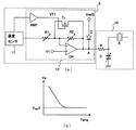
以下、本発明の実施の形態を図面に基づいて詳細に説明する。図1(a)は、本発明に係る第1の実施の形態の補償電圧回路の構成を示す図である。
補償電圧回路1は、圧電振動子Xの周囲の温度を感知する温度センサ11と、温度センサ11の温度検知結果に応じて補償電圧を発生する補償電圧発生部12と、を備える。補償電圧発生部12は、例えば演算増幅器OP、可変抵抗R1、R2及びトランジスタTrと、を備えている。
補償電圧回路1は、図1(a)に示すように、温度センサ10の出力ラインを、可変抵抗R1を介して演算増幅器OPの反転入力端子(−)に接続すると共に、基準電圧V1を非反転入力端子(+)に印加し、演算増幅器OPの反転入力端子と出力端子Aとを可変抵抗R2(帰還抵抗)を介して接続する。そして、トランジスタTrのゲート端子(第3端子)に基準電圧Vrefを印加し、ドレイン端子(第1端子)を演算増幅器OPの反転入力端子に、ソース端子(第2端子)を演算増幅器OPの出力端子Aに接続する。なお、補償電圧回路1の出力電圧Vaは、抵抗Rを介して圧電発振器10の可変容量素子Cに印加される。
Hereinafter, embodiments of the present invention will be described in detail with reference to the drawings. FIG. 1A is a diagram showing a configuration of a compensation voltage circuit according to the first embodiment of the present invention.
The
As shown in FIG. 1A, the
図1(b)は温度センサ11の温度−出力電圧特性を示す図、同図(c)は、温度変化に対する補償電圧回路1の出力電圧特性を示す図である。図1(b)に示す特性の温度センサの出力電圧Vsが、可変抵抗R1を介して演算増幅器OPの反転入力端子に加えられたときの動作について説明する。
まず、図1(c)のα領域の動作について説明する。このα領域においては温度センサ11の出力電圧Vsが、そのまま演算増幅器OPによって反転増幅されるため、演算増幅器OPの出力電圧Vaとしては、図1(b)のα領域に対応した出力が得られる。このとき、トランジスタTrのゲート電圧VGATE(=Vref)がソース電圧VSOURCEよりも低い状態にあるため、トランジスタTrはOFF状態であり、トランジスタTrのドレイン−ソース間は非導通の状態となっている。
ここで、トランジスタTr(NチャネルMOSFET)の動作について補足説明する。ゲート−ソース間の電圧をVGSとすると、VGSが一定電圧VT(しきい値電圧)よりも小さいときにはトランジスタTrはOFF状態となり、ドレイン−ソース間は非導通となる。逆に大きいとON状態となり、ドレイン−ソース間が導通する。つまり、VGS<VTならばトランジスタTrはOFF状態、VGS>VTならばトランジスタはON状態となることが知られている。なお、しきい値電圧VTは、MOSFETの特性によって決まるトランジスタ固有の一定電圧であり、半導体の製造プロセスによって決まる値である。
FIG. 1B shows the temperature-output voltage characteristics of the
First, the operation in the α region in FIG. In this α region, since the output voltage Vs of the
Here, a supplementary explanation will be given of the operation of the transistor Tr (N-channel MOSFET). Assuming that the voltage between the gate and the source is V GS , when V GS is smaller than the constant voltage VT (threshold voltage), the transistor Tr is turned off and the drain and the source are not conductive. On the other hand, if it is large, it will be in the ON state and the drain-source will be conductive. That is, it is known that if V GS <VT, the transistor Tr is in an OFF state, and if V GS > VT, the transistor is in an ON state. The threshold voltage VT is a constant voltage unique to the transistor determined by the characteristics of the MOSFET, and is a value determined by the semiconductor manufacturing process.
次に、図1(b)、(c)のβ領域の動作について説明する。このβ領域においては、VGS≒VTであり、トランジスタTrのソース電圧VSOURCEがゲート電圧VGATE(=Vref)にほぼ等しい状態である。このβ領域はトランジスタTrがOFF状態から序々にON状態に移行する領域であり、トランジスタTrのソース−ドレイン間は非導通の状態から導通の状態へと序々に変化する。従って、補償電圧Vaの変化が曲線的になり、図1(c)に示すように滑らかに変化する。
次に、図1(b)、(c)のγ領域の動作について説明する。このγ領域においては、VGS>VTであり、トランジスタTrがONする領域である。このとき、トランジスタTrのソース−ドレイン間が導通するので、温度センサ11の出力電圧Vsが増加しても、VGSはVTを少し超えたところで急激にクリップされた状態となり、ほぼ一定電圧となる。
図1(d)は、補償電圧回路1の可変抵抗R1、R2を可変させて、演算増幅器OPのゲインを調整したときの温度に対する補償電圧Vaの特性で、傾斜部の所定の位置を中心として傾斜が回転するように変化する。また、図1(e)は基準電圧V1を変えることにより、補償電圧Va特性の傾斜部を図に示すように上下に移動(リファレンス調整と称す)することができる。
Next, the operation of the β region shown in FIGS. 1B and 1C will be described. In this β region, V GS ≈VT, and the source voltage V SOURCE of the transistor Tr is almost equal to the gate voltage V GATE (= Vref). This β region is a region where the transistor Tr gradually changes from the OFF state to the ON state, and the source and drain of the transistor Tr gradually change from the non-conductive state to the conductive state. Therefore, the change of the compensation voltage Va becomes a curve and smoothly changes as shown in FIG.
Next, the operation in the γ region of FIGS. 1B and 1C will be described. In this γ region, V GS > VT, and the transistor Tr is turned on. At this time, since the source-drain of the transistor Tr becomes conductive, even if the output voltage Vs of the
FIG. 1D shows characteristics of the compensation voltage Va with respect to temperature when the variable resistors R1 and R2 of the
図2は、第2の実施の形態の補償電圧回路2の構成を示す図であり、図1(a)の補償電圧回路1と異なる点は、温度センサ11と可変抵抗R1との間にゲインが調整可能なゲイン調整用増幅器AMPを挿入したことである。図1(a)に示す補償電圧回路1では、可変抵抗R1、R2を変化させて演算増幅器OPのゲインを調整した後、基準電圧V1を調整すると傾斜の回転の中心が移動し、ゲイン調整とリファレンス調整とを独立に行うことができない。しかし、図2に示す補償電圧回路2ではゲイン調整用増幅器AMPによるゲイン調整と、基準電圧V1によるリファレンス調整を互いに独立に行うことができるので、補償電圧Vaの傾斜の回転中心を移動させずに、リファレンス調整を行うことができるという利点がある。
図3は、第3の実施の形態の補償電圧回路3の構成を示す図であり、図1(a)の補償電圧回路1と異なる点は、温度センサ11の出力を、ゲイン調整用増幅器AMPを介してトランジスタTrのゲートに接続した点である。ゲイン調整用増幅器AMPの出力電圧(トランジスタTrのゲート入力電圧)をVT1とする。
FIG. 2 is a diagram illustrating a configuration of the
FIG. 3 is a diagram showing the configuration of the compensation voltage circuit 3 according to the third embodiment. The difference from the
図4(a)〜(c)は、トランジスタTrのゲート入力電圧VT1と、補償電圧回路3の出力電圧(補償電圧)Va(図3のA点の電圧)との関係を示す図である。図4(a)〜(c)から明らかなように、−40℃から20℃の温度範囲ではゲート入力電圧VT1に関わらず、補償電圧回路3の補償電圧Vaは、温度の増加につれて単調に減少する特性を示す。
約20℃以上の温度では、ゲート入力電圧VT1の温度特性に応じて、補償電圧Vaの温度特性が変化することが、シミュレーションにより明らかになった。図4(a)に示すように、ゲート入力電圧VT1が温度の増加に対し単調に減少する電圧であると、補償電圧Vaは図4(a)のγで示す温度範囲のように、温度の増加に伴い減少する特性を示す。また、ゲート入力電圧VT1が温度の増加に対し一定である電圧であると、補償電圧Vaは図4(b)のγで示す温度範囲のように、温度の増加に対しほぼ一定の特性を示す。また、ゲート入力電圧VT1が温度の増加に対し単調に増加する電圧であると、補償電圧Vaは図4(c)のγで示す温度範囲のように、温度の増加に対し増加する特性を示す。
4A to 4C are diagrams showing the relationship between the gate input voltage VT1 of the transistor Tr and the output voltage (compensation voltage) Va (voltage at point A in FIG. 3) of the compensation voltage circuit 3. As apparent from FIGS. 4A to 4C, the compensation voltage Va of the compensation voltage circuit 3 monotonously decreases as the temperature increases regardless of the gate input voltage VT1 in the temperature range of −40 ° C. to 20 ° C. The characteristics to be shown.
It has been clarified by simulation that the temperature characteristic of the compensation voltage Va changes according to the temperature characteristic of the gate input voltage VT1 at a temperature of about 20 ° C. or higher. As shown in FIG. 4 (a), when the gate input voltage VT1 is a voltage that decreases monotonously with an increase in temperature, the compensation voltage Va becomes a temperature range as indicated by γ in FIG. 4 (a). It shows a characteristic that decreases with increasing. Further, when the gate input voltage VT1 is constant with respect to the increase in temperature, the compensation voltage Va exhibits a substantially constant characteristic with respect to the increase in temperature as in the temperature range indicated by γ in FIG. 4B. . Further, when the gate input voltage VT1 is a voltage that increases monotonously with increasing temperature, the compensation voltage Va exhibits a characteristic that increases with increasing temperature as in the temperature range indicated by γ in FIG. 4C. .
図5(a)は、第4の実施の形態の補償電圧回路4の構成を示す図である。
補償電圧回路4は、補償電圧発生部12として、演算増幅器OP、可変抵抗R1、R2、n個のトランジスタTr1〜Trn、基準電圧V1、ゲインが調整可能なn個の増幅器AMP1〜AMPnを備える。
温度センサ11の出力ラインを、可変抵抗R1を介して演算増幅器OPの反転入力端子に接続すると共に、基準電圧V1を非反転入力端子に印加し、演算増幅器OPの反転入力端子と出力端子Aとを可変抵抗R2(帰還抵抗)を介して接続する。そして、温度センサ11の出力ラインを第i(i=1〜n)の増幅器AMPiの入力ラインに接続し、この増幅器AMPiの出力ラインを第iのトランジスタTriのゲート端子(第3端子)に接続する。第iのトランジスタTriのドレイン端子(第1端子)を演算増幅器OPの反転入力端子に、ソース端子(第2端子)を演算増幅器OPの出力に接続して補償電圧回路4を構成する。すなわち、n個のトランジスタTr1〜Trnの並列接続したものを、演算増幅器OPの反転入力端子と出力端子とに接続した構成とする。
FIG. 5A is a diagram illustrating a configuration of the compensation voltage circuit 4 according to the fourth embodiment.
The compensation voltage circuit 4 includes, as the
The output line of the
図5(b)は、同図(a)のi番目(i=1〜n)の増幅器AMPiの出力電圧VTi(ゲート入力電圧)の温度特性を示す図である。図5(c)は補償電圧回路4の出力電圧(補償電圧)Vaの温度特性を示す図である。温度が低い場合、n個のトランジスタTri(i=1〜n)は何れもOFFの状態であり、演算増幅器OPのみが動作する。そのときの補償電圧Vaの温度特性は図5(c)のαで示す範囲のようになる。
温度が上昇するにつれて、ゲート入力電圧Vtiの高いものからトランジスタTriが次々にONし、そのゲート入力電圧Vtiによるソース電流が流れ、補償電圧Vaを得る。従って、補償電圧Vaは、折れ線状に接続された特性となる。しかも、温度と補償電圧Vaとの関係を表す直線と直線との接続点の近傍は、滑らかな曲線を呈するのが本発明の特徴である。このように、ゲインの調整できる複数の増幅器AMPiと、複数のトランジスタTriを用いることにより、補償電圧Vaの温度特性をより滑らかにすることが可能とり、ひいては、温度補償型圧電発振器の温度特性を滑らかにし、周波数ディップの発生を抑圧する効果がある。
FIG. 5B is a graph showing the temperature characteristics of the output voltage VTi (gate input voltage) of the i-th (i = 1 to n) amplifier AMPi in FIG. FIG. 5C is a diagram showing the temperature characteristics of the output voltage (compensation voltage) Va of the compensation voltage circuit 4. When the temperature is low, all the n transistors Tri (i = 1 to n) are in the OFF state, and only the operational amplifier OP operates. The temperature characteristic of the compensation voltage Va at that time is in the range indicated by α in FIG.
As the temperature rises, the transistors Tri are turned on one after another from the one with the higher gate input voltage Vti, the source current by the gate input voltage Vti flows, and the compensation voltage Va is obtained. Therefore, the compensation voltage Va has a characteristic of being connected in a polygonal line shape. Moreover, it is a feature of the present invention that the vicinity of the connection point between the straight lines representing the relationship between the temperature and the compensation voltage Va exhibits a smooth curve. Thus, by using a plurality of amplifiers AMPi whose gain can be adjusted and a plurality of transistors Tri, the temperature characteristic of the compensation voltage Va can be made smoother. It has the effect of smoothing and suppressing the occurrence of frequency dip.
図6は、第5の実施の形態の補償電圧回路5の構成を示す図である。図3に示した補償電圧回路3と異なる点は、演算増幅器OPの出力端子AにダイオードDのアノード端子を接続し、このダイオードDのカソードに基準電圧Vref3を印加した点である。温度が上昇して演算増幅器OPの出力電圧(補償電圧Va)が、基準電圧Vref3より低くなると、ダイオードDが順バイアスとなり、A点の電圧はクリップ電圧Vref3となる。更に温度が上昇すると演算増幅器OPの出力電圧は更に低下するが、クリップ電圧Vref3によりクリップされているので、図6(b)に示すごとく一定電圧Vref3となる。 FIG. 6 is a diagram illustrating a configuration of the compensation voltage circuit 5 according to the fifth embodiment. The difference from the compensation voltage circuit 3 shown in FIG. 3 is that the anode terminal of the diode D is connected to the output terminal A of the operational amplifier OP, and the reference voltage Vref3 is applied to the cathode of the diode D. When the temperature rises and the output voltage (compensation voltage Va) of the operational amplifier OP becomes lower than the reference voltage Vref3, the diode D becomes forward biased, and the voltage at the point A becomes the clip voltage Vref3. When the temperature further rises, the output voltage of the operational amplifier OP further decreases, but since it is clipped by the clip voltage Vref3, it becomes a constant voltage Vref3 as shown in FIG.
図7(a)は、第6の実施の形態の補償電圧回路6の構成を示す図である。図7(a)に示す補償電圧回路6のうち、ゲイン調整用増幅器AMP1、可変抵抗R1、R2、演算増幅器OP1、及びトランジスタTr1(NチャネルMOSFET)を備えた第1の補償電圧発生部は、図2に示した補償電圧発生部12と同じ回路構成であり、その作用も同じである。つまり、温度センサ11の出力電圧Vsが、図7(b)に示すような温度の上昇に伴い直線的に増加する特性であると、演算増幅器OP1の出力端子A1における電圧Va1の温度特性は、図7(c)に示すような特性となる。
図7(a)に示す補償電圧回路6のうち、ゲイン調整用増幅器AMP2、可変抵抗R3、R4、演算増幅器OP2、及びトランジスタTr2(PチャネルMOSFET)を備えた第2の補償電圧発生部は、図2に示した補償電圧回路2とほぼ同じ回路構成であるが、ゲイン調整用増幅器AMP2が反転増幅器であり、トランジスタTr2がPチャネルMOSFETである点が異なる。
この場合、第2の補償電圧発生部の補償電圧Va2の特性は、図7(d)に示すような特性となる。従って、演算増幅器OP1の出力電圧Va1と、演算増幅器OP2の出力電圧Va2とを加算器Kに入力することにより、加算器Kの出力電圧、即ち補償電圧回路6の補償電圧Va3は、図7(e)示すような負の3次曲線を呈する特性となる。このような補償電圧Va3は、3次曲線を呈する圧電振動子の補償電圧として用いることにより、可変容量素子を1個のみ有する発振回路の温度補償を行うことができる。
FIG. 7A is a diagram illustrating a configuration of the compensation voltage circuit 6 according to the sixth embodiment. Of the compensation voltage circuit 6 shown in FIG. 7A, a first compensation voltage generator including a gain adjusting amplifier AMP1, variable resistors R1 and R2, an operational amplifier OP1, and a transistor Tr1 (N-channel MOSFET) includes: The circuit configuration is the same as that of the
Of the compensation voltage circuit 6 shown in FIG. 7A, a second compensation voltage generator including a gain adjusting amplifier AMP2, variable resistors R3 and R4, an operational amplifier OP2, and a transistor Tr2 (P-channel MOSFET) includes: The circuit configuration is almost the same as that of the
In this case, the characteristic of the compensation voltage Va2 of the second compensation voltage generator is as shown in FIG. Therefore, by inputting the output voltage Va1 of the operational amplifier OP1 and the output voltage Va2 of the operational amplifier OP2 to the adder K, the output voltage of the adder K, that is, the compensation voltage Va3 of the compensation voltage circuit 6 is shown in FIG. e) The characteristic exhibits a negative cubic curve as shown. By using such a compensation voltage Va3 as a compensation voltage of a piezoelectric vibrator exhibiting a cubic curve, it is possible to perform temperature compensation of an oscillation circuit having only one variable capacitance element.
図8は、温度補償型圧電発振器の構成を示す回路図であり、その補償電圧回路6は、図7(a)に示した補償電圧回路6から加算器Kを取り除いたものである。補償電圧回路6の演算増幅器OP1、OP2の夫々の補償電圧Va1、Va2を、圧電発振器10の2つの可変容量素子Cv1、Cv2に夫々接続した例である。圧電発振器10は、図8に示すように増幅器AI、2つの容量C1、C2、圧電振動子X、及び2つの可変容量素子Cv1、Cv2を備えた周知の発振器である。補償電圧回路6の演算増幅器OP1の出力電圧(補償電圧Va1)を、抵抗R6を介して可変容量素子Cv1の一方の端子に接続し、可変容量素子Cv1の他方の端子は接地する。そして、補償電圧回路6の演算増幅器OP2の出力(補償電圧Va2)を、抵抗R7を介して可変容量素子Cv2の一方の端子に接続し、可変容量素子Cv2の他方の端子は接地する。周波数温度特性が3次曲線を呈する圧電振動子Xの常温より低温側の温度補償は、図7(c)に示す補償電圧Va1を可変容量素子Cv1に加えることにより行う。また、常温より高温側の温度補償に関しては、図7(d)に示す補償電圧特性を有する電圧Va2を可変容量素子Cv2に加えることにより、温度補償を行うことができる。
FIG. 8 is a circuit diagram showing the configuration of the temperature-compensated piezoelectric oscillator, and the compensation voltage circuit 6 is obtained by removing the adder K from the compensation voltage circuit 6 shown in FIG. In this example, the compensation voltages Va1 and Va2 of the operational amplifiers OP1 and OP2 of the compensation voltage circuit 6 are connected to the two variable capacitance elements Cv1 and Cv2 of the
図9は、温度補償型圧電発振器の構成を示す回路図であり、その補償電圧回路6は、図8に示した補償電圧回路6と基本的には同じであるが、トランジスタTr2がNチャネルMOSFETであり、AMP2が反転増幅器であるところが異なる。(その理由は後述する。)本実施例は補償電圧回路6からの2つの補償電圧Va1、Va2を、低温用MOS容量素子ML、高温用MOS容量素子MHを有する圧電発振器10に適用した例である。圧電発振器10は、周知のように、例えばコルピッツ型発振回路と、温度補償回路と、を備えている。コルピッツ型発振回路は、圧電振動子Xと、トランジスタTr10と、複数の容量と、複数の抵抗と、を備えている。
また、温度補償回路は、例えば低温用MOS容量素子MLと容量C14との直列回路に、高温用MOS容量素子MHを並列接続し、低温用MOS容量素子MLのゲートに容量C15の一方の端子を接続し、他方の端子を接地する。
更に、低温用MOS容量素子MLと高温用MOS容量素子MHとの接続点に基準電圧Vref8を印加する。補償電圧回路6の演算増幅器OP1の補償電圧Va1を、抵抗R14を介して低温用MOS容量素子MLのバックゲートに接続し、演算増幅器OP2の補償電圧Va2を、抵抗R15を介して高温用MOS容量素子MHのゲートに接続して、温度補償型圧電発振器を構成する。
FIG. 9 is a circuit diagram showing the configuration of a temperature compensated piezoelectric oscillator. The compensation voltage circuit 6 is basically the same as the compensation voltage circuit 6 shown in FIG. 8, but the transistor Tr2 is an N-channel MOSFET. The difference is that AMP2 is an inverting amplifier. (The reason will be described later.) This embodiment is an example in which two compensation voltages Va1 and Va2 from the compensation voltage circuit 6 are applied to a
In addition, the temperature compensation circuit includes, for example, a high-temperature MOS capacitor element MH connected in parallel to a series circuit of a low-temperature MOS capacitor element ML and a capacitor C14, and one terminal of the capacitor C15 is connected to the gate of the low-temperature MOS capacitor element ML. Connect and ground the other terminal.
Further, the reference voltage Vref8 is applied to the connection point between the low temperature MOS capacitor element ML and the high temperature MOS capacitor element MH. The compensation voltage Va1 of the operational amplifier OP1 of the compensation voltage circuit 6 is connected to the back gate of the low-temperature MOS capacitor element ML via the resistor R14, and the compensation voltage Va2 of the operational amplifier OP2 is connected to the high-temperature MOS capacitor via the resistor R15. A temperature compensated piezoelectric oscillator is configured by connecting to the gate of the element MH.
ここで、トランジスタTr2をNチャネルMOSFETとし、AMP2が反転している理由について説明する。これは、補償電圧Va1が低温用MOS容量素子MLのバックゲート側に印加されているのに対し、補償電圧Va2が高温用MOS容量素子MHのゲート側に印加されているからである。つまり、温度増加に対して一定電圧(低電圧)の状態から単調増加する電圧特性を得る目的で、補償電圧Va2(高温補償用)の回路はこのような構成となっている。
以上説明したように、本発明の補償電圧回路6から生成される滑らかな補償電圧を、温度補償回路に印加することにより、圧電振動子の周波数補償精度が改善されると共に、補償電圧の直線同士の接続部が滑らかに形成されているので、周波数ディップの発生を抑圧することができるという効果がある。
Here, the reason why the transistor Tr2 is an N-channel MOSFET and the AMP2 is inverted will be described. This is because the compensation voltage Va1 is applied to the back gate side of the low temperature MOS capacitor element ML, whereas the compensation voltage Va2 is applied to the gate side of the high temperature MOS capacitor element MH. That is, the circuit of the compensation voltage Va2 (for high temperature compensation) has such a configuration for the purpose of obtaining voltage characteristics that monotonously increase from a constant voltage (low voltage) state with respect to temperature increase.
As described above, by applying the smooth compensation voltage generated from the compensation voltage circuit 6 of the present invention to the temperature compensation circuit, the frequency compensation accuracy of the piezoelectric vibrator is improved, and the straight lines of the compensation voltage are connected to each other. Since the connecting portion is smoothly formed, the occurrence of frequency dip can be suppressed.
1、2、3、4、5、6…補償電圧回路、10…発振器、11…温度センサ、12…補償電圧発生部、R、R1、R2、R3、R4、R6、R7、R11、R12、R14、R15、R16…抵抗、C、C1、C2、C11、C12、C14、C15…容量、Cv1、Cv2…可変容量素子、Vs…温度センサの出力電圧、V1、V3、Vref、Vref2、Vref3、Vref4…基準電圧、OP、OP1、OP2…演算増幅器、Tr、Tr1、Tr2、Trn…トランジスタ、AMP、AMP1、AMP2、AMPn…ゲイン調整用増幅器、VT1、VT2、VTn…増幅器の出力、Va、Va1、Va2、Va3…補償電圧、K…加算器 1, 2, 3, 4, 5, 6 ... compensation voltage circuit, 10 ... oscillator, 11 ... temperature sensor, 12 ... compensation voltage generator, R, R1, R2, R3, R4, R6, R7, R11, R12, R14, R15, R16 ... resistor, C, C1, C2, C11, C12, C14, C15 ... capacitance, Cv1, Cv2 ... variable capacitance element, Vs ... output voltage of temperature sensor, V1, V3, Vref, Vref2, Vref3, Vref4 ... reference voltage, OP, OP1, OP2 ... operational amplifier, Tr, Tr1, Tr2, Trn ... transistor, AMP, AMP1, AMP2, AMPn ... gain adjusting amplifier, VT1, VT2, VTn ... amplifier output, Va, Va1 , Va2, Va3 ... compensation voltage, K ... adder
Claims (7)
トランジスタ、前記温度センサの出力信号を増幅する演算増幅器およびゲイン調整を行うゲイン調整用増幅器を有している補償電圧発生部と、を備え、 A compensation voltage generator having a transistor, an operational amplifier that amplifies the output signal of the temperature sensor, and a gain adjustment amplifier that performs gain adjustment,
前記温度センサの出力信号端子ならびに前記トランジスタの第1端子と前記演算増幅器の反転入力端子が接続されており、かつ前記トランジスタの第2端子と前記演算増幅器の出力端子が接続されており、 The output signal terminal of the temperature sensor and the first terminal of the transistor and the inverting input terminal of the operational amplifier are connected, and the second terminal of the transistor and the output terminal of the operational amplifier are connected,
前記出力信号端子と前記トランジスタの第3端子との間に前記ゲイン調整用増幅器が接続されており、前記温度センサの温度検知結果に応じた補償電圧を発生することを特徴とする補償電圧回路。 The compensation voltage circuit, wherein the gain adjusting amplifier is connected between the output signal terminal and the third terminal of the transistor, and generates a compensation voltage according to a temperature detection result of the temperature sensor.
Priority Applications (1)
| Application Number | Priority Date | Filing Date | Title |
|---|---|---|---|
| JP2007246667A JP5119826B2 (en) | 2007-09-25 | 2007-09-25 | Compensation voltage circuit and temperature compensated piezoelectric oscillator |
Applications Claiming Priority (1)
| Application Number | Priority Date | Filing Date | Title |
|---|---|---|---|
| JP2007246667A JP5119826B2 (en) | 2007-09-25 | 2007-09-25 | Compensation voltage circuit and temperature compensated piezoelectric oscillator |
Publications (3)
| Publication Number | Publication Date |
|---|---|
| JP2009077342A JP2009077342A (en) | 2009-04-09 |
| JP2009077342A5 JP2009077342A5 (en) | 2010-11-11 |
| JP5119826B2 true JP5119826B2 (en) | 2013-01-16 |
Family
ID=40611856
Family Applications (1)
| Application Number | Title | Priority Date | Filing Date |
|---|---|---|---|
| JP2007246667A Active JP5119826B2 (en) | 2007-09-25 | 2007-09-25 | Compensation voltage circuit and temperature compensated piezoelectric oscillator |
Country Status (1)
| Country | Link |
|---|---|
| JP (1) | JP5119826B2 (en) |
Families Citing this family (2)
| Publication number | Priority date | Publication date | Assignee | Title |
|---|---|---|---|---|
| EP3367570A1 (en) * | 2017-02-23 | 2018-08-29 | Rakon Limited | Temperature compensated crystal oscillator |
| CN116094476A (en) * | 2023-04-11 | 2023-05-09 | 上海安其威微电子科技有限公司 | Circuit structure with gain compensation |
Family Cites Families (13)
| Publication number | Priority date | Publication date | Assignee | Title |
|---|---|---|---|---|
| JPH03126304A (en) * | 1989-10-12 | 1991-05-29 | Fujitsu Ltd | Temperature compensation crystal oscillator |
| JP3198001B2 (en) * | 1993-12-08 | 2001-08-13 | 株式会社明電舎 | Digital temperature compensated crystal oscillator |
| JP3310494B2 (en) * | 1995-05-25 | 2002-08-05 | 株式会社明電舎 | Digital temperature compensated crystal oscillator |
| JPH10322128A (en) * | 1997-05-15 | 1998-12-04 | Matsushita Electric Ind Co Ltd | Temperature-compensating device for piezoelectric oscillator |
| JP2000114875A (en) * | 1998-10-02 | 2000-04-21 | Toyo Commun Equip Co Ltd | Oscillator |
| JP3847021B2 (en) * | 1999-03-30 | 2006-11-15 | 沖電気工業株式会社 | Voltage controlled oscillator |
| JP2001196857A (en) * | 2000-01-12 | 2001-07-19 | Toyo Commun Equip Co Ltd | Crystal oscillator |
| JP3433720B2 (en) * | 2000-03-24 | 2003-08-04 | セイコーエプソン株式会社 | Oscillation circuit |
| JP2003101408A (en) * | 2001-09-21 | 2003-04-04 | Citizen Watch Co Ltd | Oscillator |
| JP4424001B2 (en) * | 2004-02-20 | 2010-03-03 | エプソントヨコム株式会社 | Temperature compensated piezoelectric oscillator |
| JP2006319388A (en) * | 2005-05-10 | 2006-11-24 | Jaitoronikusu:Kk | Automatic gain control circuit and sine wave oscillation circuit employing the same |
| JP4852969B2 (en) * | 2005-10-25 | 2012-01-11 | ミツミ電機株式会社 | Oscillator circuit |
| JP2007157890A (en) * | 2005-12-02 | 2007-06-21 | Matsushita Electric Ind Co Ltd | Semiconductor integrated circuit and semiconductor device |
-
2007
- 2007-09-25 JP JP2007246667A patent/JP5119826B2/en active Active
Also Published As
| Publication number | Publication date |
|---|---|
| JP2009077342A (en) | 2009-04-09 |
Similar Documents
| Publication | Publication Date | Title |
|---|---|---|
| CN107017838B (en) | Circuit device, oscillator, electronic apparatus, and moving object | |
| JP2010130141A (en) | Voltage controlled temperature compensation piezoelectric oscillator | |
| KR20020059654A (en) | Temperature compensation oscillator | |
| JPH0918234A (en) | Temperature compensated piezoelectric oscillator | |
| JP2013211654A (en) | Oscillator, electronic apparatus and temperature compensation method for oscillator | |
| JP6759777B2 (en) | Manufacturing method of temperature-compensated oscillator circuit, oscillator, electronic device, mobile body and oscillator | |
| US10027331B2 (en) | Oscillator, electronic apparatus, and moving object | |
| US20060017517A1 (en) | Voltage controlled oscillator | |
| US5004988A (en) | Quartz crystal oscillator with temperature-compensated frequency characteristics | |
| US7268636B2 (en) | Voltage controlled oscillator | |
| JP5119826B2 (en) | Compensation voltage circuit and temperature compensated piezoelectric oscillator | |
| JP6377192B2 (en) | Temperature compensated crystal oscillator | |
| JP5034772B2 (en) | Temperature compensated piezoelectric oscillator | |
| US7847645B2 (en) | Oscillation control apparatus and oscillator | |
| JP5311545B2 (en) | Oscillator | |
| JP2002135051A (en) | Piezoelectric oscillator | |
| JP4428124B2 (en) | Temperature compensated oscillator | |
| JP2002026658A (en) | Quartz oscillator circuit | |
| JP2010183366A (en) | Temperature compensated oscillation circuit | |
| JP5556928B2 (en) | Temperature compensated voltage generation circuit, temperature compensated oscillation circuit | |
| JP5178457B2 (en) | Oscillator | |
| JP4314988B2 (en) | Temperature compensated piezoelectric oscillator | |
| JPH1093343A (en) | Temperature compensation method for piezoelectric oscillating circuit | |
| JP2008294850A (en) | Function generating circuit | |
| JP4311313B2 (en) | Piezoelectric oscillator |
Legal Events
| Date | Code | Title | Description |
|---|---|---|---|
| A521 | Written amendment |
Free format text: JAPANESE INTERMEDIATE CODE: A523 Effective date: 20100922 |
|
| A621 | Written request for application examination |
Free format text: JAPANESE INTERMEDIATE CODE: A621 Effective date: 20100922 |
|
| A711 | Notification of change in applicant |
Free format text: JAPANESE INTERMEDIATE CODE: A712 Effective date: 20110729 |
|
| RD03 | Notification of appointment of power of attorney |
Free format text: JAPANESE INTERMEDIATE CODE: A7423 Effective date: 20110729 |
|
| A521 | Written amendment |
Free format text: JAPANESE INTERMEDIATE CODE: A523 Effective date: 20110819 |
|
| A131 | Notification of reasons for refusal |
Free format text: JAPANESE INTERMEDIATE CODE: A131 Effective date: 20120529 |
|
| A521 | Written amendment |
Free format text: JAPANESE INTERMEDIATE CODE: A523 Effective date: 20120724 |
|
| TRDD | Decision of grant or rejection written | ||
| A01 | Written decision to grant a patent or to grant a registration (utility model) |
Free format text: JAPANESE INTERMEDIATE CODE: A01 Effective date: 20120925 |
|
| A01 | Written decision to grant a patent or to grant a registration (utility model) |
Free format text: JAPANESE INTERMEDIATE CODE: A01 |
|
| A61 | First payment of annual fees (during grant procedure) |
Free format text: JAPANESE INTERMEDIATE CODE: A61 Effective date: 20121008 |
|
| FPAY | Renewal fee payment (event date is renewal date of database) |
Free format text: PAYMENT UNTIL: 20151102 Year of fee payment: 3 |
|
| R150 | Certificate of patent or registration of utility model |
Free format text: JAPANESE INTERMEDIATE CODE: R150 Ref document number: 5119826 Country of ref document: JP Free format text: JAPANESE INTERMEDIATE CODE: R150 |
|
| S531 | Written request for registration of change of domicile |
Free format text: JAPANESE INTERMEDIATE CODE: R313531 |
|
| R350 | Written notification of registration of transfer |
Free format text: JAPANESE INTERMEDIATE CODE: R350 |