JP5114849B2 - Electrical inspection method for printed wiring boards - Google Patents
Electrical inspection method for printed wiring boards Download PDFInfo
- Publication number
- JP5114849B2 JP5114849B2 JP2006034818A JP2006034818A JP5114849B2 JP 5114849 B2 JP5114849 B2 JP 5114849B2 JP 2006034818 A JP2006034818 A JP 2006034818A JP 2006034818 A JP2006034818 A JP 2006034818A JP 5114849 B2 JP5114849 B2 JP 5114849B2
- Authority
- JP
- Japan
- Prior art keywords
- land
- inspection
- circuit
- printed wiring
- measuring
- Prior art date
- Legal status (The legal status is an assumption and is not a legal conclusion. Google has not performed a legal analysis and makes no representation as to the accuracy of the status listed.)
- Expired - Fee Related
Links
Images

Description
本発明は、パソコン、移動体通信機器、ビデオカメラ、デジタルカメラ等の各種電子機器に用いられるプリント配線板の電気検査方法に関するものである。 The present invention relates to an electrical inspection method for printed wiring boards used in various electronic devices such as personal computers, mobile communication devices, video cameras, and digital cameras.
プリント配線板の導体回路の断線状態を検出する電気検査としては、従来より2端子検査が広く用いられていた。ところが近年のプリント配線板の高密度化に伴う導体の細線化、スルーホールの小径化によって、以前よりも高い検査精度が必要となってきた。特に細線導体回路の部分欠損や細り、スルーホールめっきのクラックやめっき厚小といった微小な抵抗値変化の検出が要求されてきている。さらに、近年普及してきたビアに導電性ペーストを充填することによって層間の電気的な接続を行うタイプのプリント配線板においては、導電性ペーストの充填不足といった潜在的不具合を検出することが製品の品質を保証する上で必須となってきた。 Conventionally, a two-terminal inspection has been widely used as an electrical inspection for detecting a disconnection state of a conductor circuit of a printed wiring board. However, with the recent increase in the density of printed wiring boards, the finer conductors and the smaller diameters of through-holes have required higher inspection accuracy than before. In particular, it has been required to detect minute changes in resistance value such as partial defects or thinning of a thin wire conductor circuit, cracks in through-hole plating, and small plating thickness. In addition, in printed wiring boards of the type that make electrical connection between layers by filling conductive paste into vias that have become widespread in recent years, it is possible to detect potential defects such as insufficient filling of conductive paste. It has become essential to guarantee.
これらの要求に対応するためには、数十mΩオーダーの微小な抵抗値の上昇を検出しなければならない。2端子検査によれば検査用端子と被検査部であるプリント配線板のランドとの間の接触抵抗および、検査用端子と検査機器とを結ぶリード線の抵抗、更にはコンタクトプローブの抵抗が被検査物の抵抗に含まれる。そのため2端子検査はこの抵抗が無視できるような完全な断線状態などの高抵抗の検出には有効であるが、上記の微小な抵抗値の上昇の検出には不向きである。 In order to meet these requirements, it is necessary to detect a slight increase in resistance value on the order of several tens of mΩ. According to the two-terminal inspection, the contact resistance between the inspection terminal and the land of the printed wiring board that is the part to be inspected, the resistance of the lead wire connecting the inspection terminal and the inspection device, and further the resistance of the contact probe are covered. Included in inspection resistance. Therefore, the two-terminal inspection is effective for detecting a high resistance such as a complete disconnection state in which this resistance can be ignored, but is not suitable for detecting the above-described small increase in resistance value.
そこで最近では2端子検査に替わって検査用端子の接触抵抗等の影響を受けない4端子検査が普及してきた。特に前述の導電性ペーストを充填したビアの導通保証のための検査には不可欠であると言える。 Therefore, recently, a four-terminal inspection that is not affected by the contact resistance of the inspection terminal has become widespread instead of the two-terminal inspection. In particular, it can be said that it is indispensable for the inspection for ensuring the continuity of the via filled with the conductive paste.
図3は従来のプリント配線板の電気検査方法を示す概略図であり、スルーホール21を有するプリント配線板22においてランド23a−23b間を4端子検査によって検査する例を示したものである。以下、図3を用いて従来のプリント配線板の電気検査方法について説明する。
FIG. 3 is a schematic diagram showing a conventional method for inspecting a printed wiring board, and shows an example of inspecting a
図3において、ランド23a、23bの各々に電流供給用プロープ24a、24bを接触させ、被検査回路である23a−23b間に電流を供給する。その一方で同様にランド23a、23bの各々に接触させた電圧測定用プローブ25a、25bによって、23a−23b間の電圧を測定し、測定した電圧の値から23a−23b間の抵抗値が算出される。そして、予め抵抗値の判定基準を設定しておくことによって検査の合否を判定することができる。
In FIG. 3, the
上記の従来のプリント配線板の検査方法においては、一方のランド23aに接触させる電流供給用プローブ24aと電圧測定用プローブ25aを対とすることにより、2本のプローブがお互いに離れないように揃えるといった等の発明が各種提唱されている。
In the conventional printed wiring board inspection method described above, the
この発明に関連する先行技術文献としては、例えば、特許文献1が知られている。
しかしながら、前記従来のプリント配線板の電気検査方法では以下の課題を有していた。 However, the conventional electrical inspection method for printed wiring boards has the following problems.
パソコン、移動体通信機器、ビデオカメラ、デジタルカメラ等に使用される高密度なプリント配線板に実装される電子部品は現在ではCSPが主流となり、これを実装するランドの直径はφ0.3mmあるいはそれ以下のものとなってきた。通常、電気検査においてはこれらの実装用のランドをそのまま検査用ランドとして用いるので、径が小さいランドに対して検査用プローブの先端を精度よく位置合わせする必要がある。 Electronic components mounted on high-density printed wiring boards used in personal computers, mobile communication devices, video cameras, digital cameras, etc. are now predominantly CSP, and the land on which they are mounted has a diameter of φ0.3 mm or more. It has become the following. Usually, in an electrical inspection, these mounting lands are used as inspection lands as they are, and therefore it is necessary to accurately align the tip of the inspection probe with respect to a land having a small diameter.
ところが前記従来のプリント配線板の電気検査方法によれば、2本のプローブを1つのランドに接触させなければならず、その位置合わせは一層困難なものとなる。そのために、電気検査工程においてしばしば位置合わせ不具合が発生し、本来良品である製品が不良品と誤判定され、位置合わせのための検査治具の微調整を頻繁に行わなければならなかった。このことが原因となって、検査工程の検査効率が低下し、さらに作業者に対する作業の負荷が増大していた。 However, according to the conventional method for inspecting a printed wiring board, two probes must be brought into contact with one land, and the alignment becomes more difficult. For this reason, an alignment defect often occurs in the electrical inspection process, and a product that is originally a good product is erroneously determined as a defective product, and fine adjustment of an inspection jig for alignment has to be frequently performed. As a result, the inspection efficiency of the inspection process is reduced, and the work load on the worker is increased.
また、小径ランドに接触させる2本のプローブは、プローブ同士がお互いに接触しないようにするためにその径を小さくしなければならず、材料費、加工費が増大していた。 In addition, the two probes brought into contact with the small-diameter land have to be reduced in diameter in order to prevent the probes from contacting each other, resulting in an increase in material costs and processing costs.
本発明は前記従来の課題を解決するものであり、電気検査工程において4端子検査が元々有する抵抗値を高精度で測定するという効果を発揮すると同時に、高い検査効率を確保し、安定した検査を安価で行うことができるプリント配線板の電気検査方法を提供することを目的とする。 The present invention solves the above-mentioned conventional problems, and at the same time exerts the effect of measuring the resistance value originally possessed by the four-terminal inspection in the electrical inspection process with high accuracy, and at the same time ensures high inspection efficiency and performs stable inspection. An object of the present invention is to provide an electrical inspection method for a printed wiring board that can be performed at low cost.
前記従来の課題を解決するために、本発明は、上面および下面それぞれに設けられた電流を供給するランド及び電圧を測定するランドと、上下に隣接する各層を層間接続する導電性ペーストが充填されたビアと、前記ビアを介して前記ランドと接続する回路とを有するプリント配線板において、上下に隣接する内層の回路間を層間接続する導電性ペーストが充填された前記ビアの抵抗値を測定する電気検査方法であって、電流を供給する前記ランドと電圧を測定する前記ランドは、直下のビアにより内層の回路と接続され、電流を供給する前記ランドに接続する回路と電圧を測定する前記ランドに接続する回路は、抵抗値を測定する前記ビアの直上および直下において合流しており、上面と下面の電流を供給するランドを介して前記ビアに電流を供給し、上面と下面のランド間の電圧を測定することを特徴とするプリント配線板の電気検査方法である。 In order to solve the above-described conventional problems, the present invention includes a land for supplying current and a land for measuring voltage provided on each of the upper surface and the lower surface, and a conductive paste for interlayer connection between upper and lower layers. In a printed wiring board having a via and a circuit connected to the land via the via, a resistance value of the via filled with a conductive paste for interlayer connection between upper and lower inner-layer circuits is measured. In the electrical inspection method, the land for supplying a current and the land for measuring a voltage are connected to an inner layer circuit by a via immediately below, and the circuit for connecting to the land for supplying a current and the land for measuring a voltage are connected. connecting to the circuit are merged immediately above and immediately below the via measuring the resistance value, electrostatic the vias through the land supplying upper and lower surfaces of the current Supplying an electrical inspection method of a printed wiring board and measuring the voltage between the upper and lower surfaces of the land.
この構成により、電流供給用ランドと電圧測定用ランドは別々のランドを用いるので、1つのランドに対して1本のプローブを接触させればよく、ランドに対するプローブの位置合わせが容易となる。そのため、位置合わせ不具合による検査の誤判定がなくなり、位置合わせのための検査治具の微調整を行う必要もなく、効率よく安定した検査を行うことができる。また各導体回路の端点それぞれに2本のプローブを接触させる場合と比較して、検査治具の作製の上でコスト増加要因となる径の小さいプローブの使用本数を減少させることができ、材料費、加工費を削減することができる。 With this configuration, since the current supply land and the voltage measurement land use different lands, one probe may be brought into contact with one land, and the probe can be easily aligned with the land. For this reason, erroneous determination of inspection due to misalignment is eliminated, and it is not necessary to finely adjust the inspection jig for alignment, and efficient and stable inspection can be performed. In addition, compared with the case where two probes are brought into contact with each end point of each conductor circuit, the number of probes having a small diameter, which causes an increase in cost in the production of the inspection jig, can be reduced. , Processing costs can be reduced.
また本発明は、被検査部が層間接続を行うペーストが充填されたビアもしくはめっきが形成されたスルーホールを含むプリント配線板の電気検査方法である。 Further, the present invention is an electrical inspection method for a printed wiring board including a via or a through hole in which a portion to be inspected is filled with a paste for performing interlayer connection.
この構成により、層間接続を行うペーストが充填されたビアもしくはめっきが形成されたスルーホールの電気的接続信頼性を効率の良い作業方法により4端子検査で保証することができる。 With this configuration, it is possible to ensure electrical connection reliability of a via filled with a paste for performing interlayer connection or a through hole formed with plating by a four-terminal inspection by an efficient work method.
また本発明は、電流を供給するランドへの接続回路と電圧を測定するランドへの接続回路がビアもしくはスルーホールの直下および直上においてそれぞれ分岐していることを特徴とするプリント配線板の電気検査方法である。 According to another aspect of the present invention, there is provided an electrical inspection of a printed wiring board, wherein a connection circuit to a land for supplying a current and a connection circuit to a land for measuring a voltage are branched directly below and immediately above a via or a through hole. Is the method.
この構成により、ビアもしくはスルーホール以外の抵抗値を除いた、ビアもしくはスルーホールのみの抵抗値を測定することによって電気的接続信頼性を保証することができる。4端子検査においては原理的に電流を供給する回路と電圧を測定する回路とが交わって共通している部分の回路の抵抗値が測定される。本発明では電流を供給するランドへの接続回路と電圧を測定するランドへの接続回路がビアもしくはスルーホールの直下および直上においてそれぞれ分岐しているので、電流を供給する回路と電圧を測定する回路はビアもしくはスルーホールの直下および直上で交わり、ビアもしくはスルーホールのみの抵抗値を測定することができる。 With this configuration, electrical connection reliability can be ensured by measuring the resistance value of only the via or the through hole excluding the resistance value other than the via or the through hole. In the four-terminal inspection, in principle, the resistance value of a circuit at a common portion where a circuit for supplying a current and a circuit for measuring a voltage intersect is measured. In the present invention, the connection circuit to the land for supplying current and the connection circuit to the land for measuring voltage are branched directly below and immediately above the via or through hole, respectively, so that the circuit for supplying current and the circuit for measuring voltage Can intersect just below and directly above vias or through holes, and measure the resistance of only vias or through holes.
また本発明は、プリント配線板の部品実装用のランドを、電流を供給するランドおよび電圧を測定するランドとして用いるプリント配線板の電気検査方法である。 The present invention is also an electrical inspection method for a printed wiring board using lands for mounting components on the printed wiring board as lands that supply current and lands that measure voltage.
この構成により、検査用のランドを特別に設ける必要はなく、プリント配線板が部品実装等の本来の使用目的に応じて設計された回路パターンの中から部品実装用ランドを検査用のランドとして用いることができるので、プリント配線板の高密度性を維持した状態で電気的接続信頼性を安価で効率の良い作業方法により4端子検査で保証することができる。 With this configuration, it is not necessary to provide a special inspection land, and the component mounting land is used as the inspection land from a circuit pattern in which the printed wiring board is designed according to the original use purpose such as component mounting. Therefore, the electrical connection reliability can be ensured by a four-terminal inspection by an inexpensive and efficient working method while maintaining the high density of the printed wiring board.
本発明によれば、4端子検査による電気検査工程において、電流供給用ランドと電圧測定用ランドは別々のランドを用いるので、1つのランドに対して1本のプローブを接触させればよく、ランドに対するプローブの位置合わせが容易となり、位置合わせ不具合による検査の誤判定がなくなり、位置合わせのための検査治具の微調整を行う必要もなくなる。また検査治具の作製の上で、コスト増加要因となる径の小さいプローブの使用本数を減少させることができるので、材料費、加工費を削減することができる。以上のように本発明によれば、4端子検査が元々有する抵抗値を高精度で測定するという効果を発揮すると同時に、高い検査効率を確保し、安定した検査を安価で行うプリント配線板の電気検査方法を提供することができる。 According to the present invention, since the current supply land and the voltage measurement land use different lands in the electric inspection process by the four-terminal inspection, one probe may be brought into contact with one land. This makes it easy to align the probe with respect to the substrate, eliminates erroneous determination of inspection due to misalignment, and eliminates the need for fine adjustment of the inspection jig for alignment. In addition, since the number of probes having a small diameter, which causes an increase in cost, can be reduced in producing the inspection jig, material costs and processing costs can be reduced. As described above, according to the present invention, the effect of measuring the resistance value originally possessed by the four-terminal inspection with high accuracy is demonstrated, and at the same time, the electrical resistance of the printed wiring board that ensures high inspection efficiency and performs stable inspection at low cost. An inspection method can be provided.
以下、本発明の実施の形態を図面に基づいて説明する。 Hereinafter, embodiments of the present invention will be described with reference to the drawings.
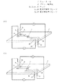
(実施の形態1)
図1は本発明の実施の形態1におけるプリント配線板の電気検査方法を示す概略図である。以下、図1を用いてスルーホール1を有するプリント配線板2の電気検査方法について説明する。
(Embodiment 1)
FIG. 1 is a schematic diagram showing an electrical inspection method for a printed wiring board according to Embodiment 1 of the present invention. Hereinafter, an electrical inspection method for the printed
ランド3a、3bの各々に電流供給用プローブ4a、4bを接触させ、3a−3b間の回路に電流を供給する。その一方で同様にランド3c、3dの各々に電圧測定用プローブ5a、5bを接触させ、3c−3d間の回路の電圧を測定し、測定した電圧の値から被検査回路の抵抗値が算出される。そして、予め抵抗値の判定基準を設定しておくことによって検査の合否を判定することができる。
The
供給する電流値は数十mA〜数百mA程度が一般的である。本実施の形態では50mAとした。また、合否の判定基準として設定する抵抗値は一律に設定してもよいが、検査を行う回路毎の正常状態での抵抗値を元に個々に設定するのがより好ましい。回路毎に導体幅、導体長、スルーホールの数および径が異なるので、それぞれの回路が持つ抵抗値も異なるためである。例えば正常状態で200mΩの回路の場合は判定値を300mΩに設定し、正常状態で400mΩの回路の場合は判定値を500mΩに設定するといった具合である。ここで回路毎の正常状態での抵抗値は良品のプリント配線板を10枚程度測定し、その平均値を計算することにより求めることができる。また、個々の判定値を設定する時の正常値からの差異は、導体幅等のバラツキの工程能力と保証すべき品質レベルを考慮して設定すればよい。 The current value to be supplied is generally about several tens mA to several hundred mA. In this embodiment, it is 50 mA. In addition, the resistance values set as pass / fail judgment criteria may be set uniformly, but it is more preferable to set them individually based on the resistance values in the normal state for each circuit to be inspected. This is because each circuit has a different conductor width, conductor length, number of through holes, and diameter, and therefore the resistance value of each circuit is different. For example, the determination value is set to 300 mΩ for a circuit of 200 mΩ in a normal state, and the determination value is set to 500 mΩ for a circuit of 400 mΩ in a normal state. Here, the resistance value in the normal state for each circuit can be obtained by measuring about 10 non-defective printed wiring boards and calculating the average value. Further, the difference from the normal value when setting each determination value may be set in consideration of the process capability of variation such as the conductor width and the quality level to be guaranteed.
電流供給用プローブ4a、4bと電圧測定用プローブ5a、5bは、従来は被検査回路の両端の同一ランドに接触させていたので、1つのランドに2本のプローブを接触させていた。本実施の形態1では図1に示すとおり、被検査部の両端の各々から分岐した各2つの回路の先端にランドを設け、一方を電流供給用に用い、他方を電圧測定用に用いた。これにより、電流供給用ランドと電圧測定用ランドは分離した別々のランドを用いることになるので、1つのランドに対して1本のプローブを接触させればよく、ランドに対するプローブの位置合わせが容易となる。そのため、位置合わせ不具合による検査の誤判定がなくなり、位置合わせのための検査治具の微調整を行う必要もなく、効率よく安定した検査を行うことができた。
Conventionally, the
4端子検査においては原理的に電流を供給する回路と電圧を測定する回路とが交わって共通している部分の回路の抵抗値が測定される。したがって電流を供給する回路と電圧を測定する回路をどの箇所で合流させるかによって検査区間が決定される。検査の目的に応じて電流を供給する回路と電圧を測定する回路が合流する箇所を選択することにより、検査区間を選択することができる。 In the four-terminal inspection, in principle, the resistance value of a circuit at a common portion where a circuit for supplying a current and a circuit for measuring a voltage intersect is measured. Accordingly, the inspection section is determined depending on where the current supplying circuit and the voltage measuring circuit are joined. An inspection section can be selected by selecting a location where a circuit that supplies current and a circuit that measures voltage meet according to the purpose of the inspection.
図1(a)は電流を供給する回路と電圧を測定する回路がそれぞれのランドの近傍で合流している。一方図1(b)は電流を供給するランドへの接続回路と電圧を測定するランドへの接続回路がスルーホール1の直下および直上においてそれぞれ分岐している。この二つを比較すると、前記4端子検査の測定原理により、図1(a)の実施例ではスルーホール1の抵抗値とスルーホール1に接続された表層の配線回路の抵抗値との合計値が測定され、図1(b)の実施例ではスルーホール1のみの抵抗値が測定される。 In FIG. 1A, a circuit for supplying current and a circuit for measuring voltage are joined in the vicinity of each land. On the other hand, in FIG. 1B, a connection circuit to a land for supplying a current and a connection circuit to a land for measuring a voltage are branched directly below and immediately above the through hole 1, respectively. When these two are compared, the total value of the resistance value of the through-hole 1 and the resistance value of the surface wiring circuit connected to the through-hole 1 in the embodiment of FIG. In the embodiment of FIG. 1B, the resistance value of only the through hole 1 is measured.
図1(a)の実施例ではスルーホール1の導通と表層の配線回路の導通を同時に保証できるという利点がある。また図1(b)の実施例では他の回路の抵抗値の影響を受けることなく、スルーホール1のみの抵抗値を単独で高精度に測定をすることができるので、スルーホール1の導通信頼性を高いレベルで保証することができるという利点がある。この場合、表層の配線回路は別途電気検査か外観画像認識検査によって保証することも可能である。 In the embodiment of FIG. 1A, there is an advantage that conduction of the through hole 1 and conduction of the wiring circuit on the surface layer can be guaranteed at the same time. In the embodiment of FIG. 1B, the resistance value of only the through hole 1 can be measured with high accuracy independently without being affected by the resistance value of other circuits. There is an advantage that the property can be guaranteed at a high level. In this case, the wiring circuit on the surface layer can be guaranteed separately by an electrical inspection or an appearance image recognition inspection.
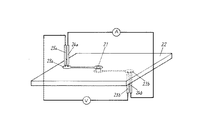
(実施の形態2)
図2は本発明の実施の形態2におけるプリント配線板の電気検査方法を示す断面図である。以下、図2を用いて導電性ペーストが充填されたビア6を有する4層で構成されたプリント配線板2の電気検査方法について説明する。
(Embodiment 2)
FIG. 2 is a cross-sectional view showing an electrical inspection method for a printed wiring board according to
形態の概要、4端子検査の原理、作用、効果は概ね実施の形態1で説明した内容と同じなので、異なる点のみを説明する。 Since the principle, operation, and effect of the four-terminal inspection are substantially the same as those described in the first embodiment, only the differences will be described.
本実施の形態で用いたプリント配線板2は図2に示すとおり、上下に隣接する各層を導電性ペーストが充填されたビア6によって電気的に接続したものである。同じ位置にビア6を上下に連結させることによって貫通スルーホールと同じ接続形態をとることもできる。また内層の必要な層同士のみを接続することにより同位置の表層部に余ったスペースを配線回路や部品実装ランドに有効利用することができる。
As shown in FIG. 2, the printed
図2(a)は電流を供給する回路と電圧を測定する回路がそれぞれのランド直下の近傍の内層部で合流している。一方図2(b)は電流を供給するランドへの接続回路と電圧を測定するランドへの接続回路が2−3層間のビア6の直下および直上においてそれぞれ分岐している。この二つを比較すると、4端子検査の測定原理により、図2(a)の実施例では2−3層間のビア6の抵抗値とビア6に接続された内層の配線回路の抵抗値との合計値が測定され、図2(b)の実施例では2−3層間のビア6のみの抵抗値が測定される。 In FIG. 2A, a circuit for supplying a current and a circuit for measuring a voltage are joined at the inner layer near the land. On the other hand, in FIG. 2B, a connection circuit to a land for supplying a current and a connection circuit to a land for measuring a voltage are branched directly below and immediately above the via 6 between the 2-3 layers. Comparing the two, according to the measurement principle of the 4-terminal inspection, in the embodiment of FIG. 2A, the resistance value of the via 6 between the 2-3 layers and the resistance value of the wiring circuit of the inner layer connected to the via 6 are The total value is measured, and in the embodiment of FIG. 2B, only the resistance value of the via 6 between the 2-3 layers is measured.
図2(a)の実施例ではビア6の導通と内層の配線回路の導通を同時に保証できるという利点がある。また図2(b)の実施例では他の回路の抵抗値の影響を受けることなく、2−3層間のビア6のみの抵抗値を単独で高精度に測定をすることができるので、ビア6の導通信頼性を高いレベルで保証することができるという利点がある。この場合、他のビアおよび表層の配線回路は別途電気検査か外観画像認識検査によって保証することも可能である。 In the embodiment of FIG. 2A, there is an advantage that conduction of the via 6 and conduction of the inner wiring circuit can be guaranteed at the same time. In the embodiment of FIG. 2B, the resistance value of only the via 6 between the 2-3 layers can be measured with high accuracy independently without being affected by the resistance value of other circuits. There is an advantage that the conduction reliability can be guaranteed at a high level. In this case, other vias and surface wiring circuits can be guaranteed separately by electrical inspection or appearance image recognition inspection.
なお、図2(a)では電流を供給する回路と電圧を測定する回路がそれぞれのランド直下の近傍の内層部で合流している例を示したが、実施の形態1と同様の方法で表層においてそれぞれのランドの近傍部で合流させることもできる。 2A shows an example in which a circuit for supplying current and a circuit for measuring voltage are merged in the inner layer portion in the vicinity immediately below each land, but the surface layer is formed by the same method as in the first embodiment. Can be combined at the vicinity of each land.
また、図2(b)では2−3層間のビア6の抵抗値を測定する例を示したが、同様の方法により他の層間のビア6の抵抗値を測定することもできる。 2B shows an example in which the resistance value of the via 6 between the 2-3 layers is measured, but the resistance value of the via 6 between other layers can be measured by the same method.
更には、実際にパソコン、移動体通信機器、ビデオカメラ、デジタルカメラ等に使用されているプリント配線板の部品実装用パターンでは、各ランド間の組合せによっては、スルーホール1またはビア6を含む導体回路と含まない導体回路が混在するので、4端子検査と2端子検査を組合わせてもよい。またランドによってはCSP実装用等の小径ランド以外にも比較的大きなランドも混在するので、小径ランドには本発明の4端子検査とし、比較的大きなランドには従来の4端子検査というように組合わせてもよい。以上のことは選択事項として適宜選択、組合せすることにより、検査効率と検査治具作製費用の面で有利な方法を提供することができる。 Furthermore, in a component mounting pattern of a printed wiring board that is actually used in a personal computer, a mobile communication device, a video camera, a digital camera, etc., a conductor including a through hole 1 or a via 6 depending on the combination between lands. Since the circuit and the conductor circuit not included are mixed, the 4-terminal inspection and the 2-terminal inspection may be combined. In addition, depending on the land, a relatively large land is also mixed in addition to a small-diameter land for CSP mounting or the like. Therefore, the 4-terminal inspection of the present invention is applied to the small-diameter land, and the conventional 4-terminal inspection is applied to the relatively large land. You may combine them. By appropriately selecting and combining the above as selection items, it is possible to provide a method that is advantageous in terms of inspection efficiency and inspection jig manufacturing cost.
以上のように本発明のプリント配線板の電子検査方法は、4端子検査による電気検査を高い検査効率で行うことができ、パソコン、移動体通信機器、ビデオカメラ、デジタルカメラ等の各種電子機器に用いられるプリント配線板の電気検査方法として有用である。 As described above, the electronic inspection method for a printed wiring board according to the present invention can perform electrical inspection by four-terminal inspection with high inspection efficiency, and can be applied to various electronic devices such as personal computers, mobile communication devices, video cameras, and digital cameras. It is useful as an electrical inspection method for the printed wiring board used.
1 スルーホール
2 プリント配線板
3a、3b ランド
4a、4b 電流供給用プローブ
5a、5b 電圧測定用プローブ
6 ビア
DESCRIPTION OF SYMBOLS 1 Through
Claims (1)
上下に隣接する各層を層間接続する導電性ペーストが充填されたビアと、
前記ビアを介して前記ランドと接続する回路とを有するプリント配線板において、
上下に隣接する内層の回路間を層間接続する導電性ペーストが充填された前記ビアの抵抗値を測定する電気検査方法であって、
電流を供給する前記ランドと電圧を測定する前記ランドは、直下のビアにより内層の回路と接続され、
電流を供給する前記ランドに接続する回路と電圧を測定する前記ランドに接続する回路は、抵抗値を測定する前記ビアの直上および直下において合流しており、
上面と下面の電流を供給するランドを介して前記ビアに電流を供給し、
上面と下面のランド間の電圧を測定することを特徴とするプリント配線板の電気検査方法。 A land for supplying current and a land for measuring voltage provided on each of the upper surface and the lower surface;
Vias filled with a conductive paste that interconnects layers adjacent to each other vertically;
In a printed wiring board having a circuit connected to the land through the via ,
An electrical inspection method for measuring a resistance value of the via filled with a conductive paste for interconnecting circuits between inner and lower adjacent circuits ,
The land for supplying a current and the land for measuring a voltage are connected to an inner layer circuit by a via immediately below,
The circuit connected to the land for supplying current and the circuit connected to the land for measuring voltage are merged immediately above and immediately below the via for measuring the resistance value,
Supplying current to the via via lands supplying current on the upper and lower surfaces;
An electrical inspection method for a printed wiring board, comprising measuring a voltage between lands on an upper surface and a lower surface.
Priority Applications (1)
| Application Number | Priority Date | Filing Date | Title |
|---|---|---|---|
| JP2006034818A JP5114849B2 (en) | 2006-02-13 | 2006-02-13 | Electrical inspection method for printed wiring boards |
Applications Claiming Priority (1)
| Application Number | Priority Date | Filing Date | Title |
|---|---|---|---|
| JP2006034818A JP5114849B2 (en) | 2006-02-13 | 2006-02-13 | Electrical inspection method for printed wiring boards |
Publications (2)
| Publication Number | Publication Date |
|---|---|
| JP2007212372A JP2007212372A (en) | 2007-08-23 |
| JP5114849B2 true JP5114849B2 (en) | 2013-01-09 |
Family
ID=38490947
Family Applications (1)
| Application Number | Title | Priority Date | Filing Date |
|---|---|---|---|
| JP2006034818A Expired - Fee Related JP5114849B2 (en) | 2006-02-13 | 2006-02-13 | Electrical inspection method for printed wiring boards |
Country Status (1)
| Country | Link |
|---|---|
| JP (1) | JP5114849B2 (en) |
Families Citing this family (7)
| Publication number | Priority date | Publication date | Assignee | Title |
|---|---|---|---|---|
| JP5188822B2 (en) * | 2008-02-04 | 2013-04-24 | 日置電機株式会社 | Board inspection equipment |
| KR20110055988A (en) * | 2009-11-20 | 2011-05-26 | 삼성전기주식회사 | Circuit board testing apparatus |
| JP5606307B2 (en) * | 2010-12-28 | 2014-10-15 | 昭和電工パッケージング株式会社 | RFID tag inspection line system |
| JP5910262B2 (en) * | 2012-04-10 | 2016-04-27 | 日本電産リード株式会社 | Inspection method of component built-in board |
| JP5450855B2 (en) * | 2013-02-25 | 2014-03-26 | 日本特殊陶業株式会社 | WIRING BOARD, IC ELECTRIC CHARACTERISTIC TESTING WIRING BOARD AND WIRING BOARD MANUFACTURING METHOD |
| JP6446791B2 (en) * | 2014-02-25 | 2019-01-09 | 日本電産リード株式会社 | Substrate inspection method, substrate inspection apparatus, inspection jig, and inspection jig set |
| CN112305405A (en) * | 2020-10-12 | 2021-02-02 | 景旺电子科技(珠海)有限公司 | Four-wire test system and test method for circuit board |
Family Cites Families (8)
| Publication number | Priority date | Publication date | Assignee | Title |
|---|---|---|---|---|
| JPH01297563A (en) * | 1988-05-26 | 1989-11-30 | Hitachi Ltd | Method and device for measuring through-hole resistance of printed board |
| JPH0420847A (en) * | 1990-05-15 | 1992-01-24 | Toshiba Corp | Inspection-pattern projecting apparatus |
| JPH06347500A (en) * | 1993-06-07 | 1994-12-22 | Canon Inc | Testing method and testing device of circuit board |
| JPH0943295A (en) * | 1995-07-28 | 1997-02-14 | Toppan Printing Co Ltd | Method of inspecting through hole defect in printed wire board and apparatus therefor |
| JPH11101841A (en) * | 1997-09-26 | 1999-04-13 | Sony Corp | Conductive paste through hole type double-sided printed wiring board and its electric characteristics inspection equipment |
| JP3291651B2 (en) * | 1998-09-18 | 2002-06-10 | 富士通株式会社 | Wiring structure for via hole resistance measurement |
| JP3835333B2 (en) * | 2002-04-04 | 2006-10-18 | 松下電器産業株式会社 | Inspection method and inspection device for printed wiring board |
| JP3981314B2 (en) * | 2002-08-28 | 2007-09-26 | 京セラ株式会社 | Manufacturing method of multilayer wiring board |
-
2006
- 2006-02-13 JP JP2006034818A patent/JP5114849B2/en not_active Expired - Fee Related
Also Published As
| Publication number | Publication date |
|---|---|
| JP2007212372A (en) | 2007-08-23 |
Similar Documents
| Publication | Publication Date | Title |
|---|---|---|
| JP5114849B2 (en) | Electrical inspection method for printed wiring boards | |
| JP4901602B2 (en) | Printed circuit board manufacturing method and printed circuit board | |
| CN103219322B (en) | There is three dimensional integrated circuits and the using method thereof of resistance measuring arrangements | |
| TWI495406B (en) | In-circuit test structure for printed circuit board | |
| JP5465980B2 (en) | Printed circuit board inspection method and inspection apparatus | |
| JP2013217796A (en) | Method of inspecting component embedded substrate | |
| US8102053B2 (en) | Displacement detection pattern for detecting displacement between wiring and via plug, displacement detection method, and semiconductor device | |
| KR101055507B1 (en) | Repair structure and repair method of pattern part | |
| KR101039049B1 (en) | Chip scale package for detecting open/short of elcectrode pettern using noncontact inspection method and the inspection apparatus thereof | |
| KR20190130603A (en) | Electrical connection device | |
| KR20150130506A (en) | Board inspection method | |
| JP5258497B2 (en) | Wiring structure for solder joint inspection of printed wiring board | |
| JP5404113B2 (en) | Circuit board pass / fail judgment method | |
| JP2008028213A (en) | Circuit board and inspection method therefor | |
| KR20140009027A (en) | Apparatus and method for inspecting board | |
| JPH06260799A (en) | Circuit board inspecting method, and circuit board | |
| JP3191205B2 (en) | Printed circuit board inspection equipment | |
| JPH10190181A (en) | Printed board and its inspecting method | |
| JP5495303B2 (en) | Semiconductor module and semiconductor module inspection method | |
| JP2003004794A (en) | Electronic component, circuit board and inspection method for solder joint of electronic component to circuit board | |
| JP2002299805A (en) | Method of checking circuit board and mounting position | |
| KR101454924B1 (en) | PCB sample for evaluating quality | |
| TWM521801U (en) | Adapting interface board with multi-layer structure with high bonding strength | |
| KR20140139885A (en) | Board inspecting apparatus and method for inspecting of the board | |
| JPH07287042A (en) | In-circuit inspection method |
Legal Events
| Date | Code | Title | Description |
|---|---|---|---|
| A621 | Written request for application examination |
Free format text: JAPANESE INTERMEDIATE CODE: A621 Effective date: 20090128 |
|
| RD01 | Notification of change of attorney |
Free format text: JAPANESE INTERMEDIATE CODE: A7421 Effective date: 20091127 |
|
| A977 | Report on retrieval |
Free format text: JAPANESE INTERMEDIATE CODE: A971007 Effective date: 20110207 |
|
| A131 | Notification of reasons for refusal |
Free format text: JAPANESE INTERMEDIATE CODE: A131 Effective date: 20110215 |
|
| A131 | Notification of reasons for refusal |
Free format text: JAPANESE INTERMEDIATE CODE: A131 Effective date: 20111206 |
|
| A521 | Written amendment |
Free format text: JAPANESE INTERMEDIATE CODE: A523 Effective date: 20111221 |
|
| A131 | Notification of reasons for refusal |
Free format text: JAPANESE INTERMEDIATE CODE: A131 Effective date: 20120508 |
|
| A521 | Written amendment |
Free format text: JAPANESE INTERMEDIATE CODE: A523 Effective date: 20120626 |
|
| TRDD | Decision of grant or rejection written | ||
| A01 | Written decision to grant a patent or to grant a registration (utility model) |
Free format text: JAPANESE INTERMEDIATE CODE: A01 Effective date: 20120918 |
|
| A01 | Written decision to grant a patent or to grant a registration (utility model) |
Free format text: JAPANESE INTERMEDIATE CODE: A01 |
|
| A61 | First payment of annual fees (during grant procedure) |
Free format text: JAPANESE INTERMEDIATE CODE: A61 Effective date: 20121001 |
|
| FPAY | Renewal fee payment (event date is renewal date of database) |
Free format text: PAYMENT UNTIL: 20151026 Year of fee payment: 3 |
|
| LAPS | Cancellation because of no payment of annual fees |