JP5113913B2 - Tandem OLED device with intermediate connection layer - Google Patents
Tandem OLED device with intermediate connection layer Download PDFInfo
- Publication number
- JP5113913B2 JP5113913B2 JP2010544995A JP2010544995A JP5113913B2 JP 5113913 B2 JP5113913 B2 JP 5113913B2 JP 2010544995 A JP2010544995 A JP 2010544995A JP 2010544995 A JP2010544995 A JP 2010544995A JP 5113913 B2 JP5113913 B2 JP 5113913B2
- Authority
- JP
- Japan
- Prior art keywords
- layer
- oled device
- alkali metal
- tandem oled
- organic
- Prior art date
- Legal status (The legal status is an assumption and is not a legal conclusion. Google has not performed a legal analysis and makes no representation as to the accuracy of the status listed.)
- Active
Links
- 239000010410 layer Substances 0.000 claims abstract description 138
- 239000012044 organic layer Substances 0.000 claims abstract description 24
- 229910052783 alkali metal Inorganic materials 0.000 claims abstract description 20
- 150000001340 alkali metals Chemical class 0.000 claims abstract description 20
- 238000005401 electroluminescence Methods 0.000 claims description 27
- 150000001875 compounds Chemical class 0.000 claims description 25
- 230000005525 hole transport Effects 0.000 claims description 17
- 229910052744 lithium Inorganic materials 0.000 claims description 16
- WHXSMMKQMYFTQS-UHFFFAOYSA-N Lithium Chemical compound [Li] WHXSMMKQMYFTQS-UHFFFAOYSA-N 0.000 claims description 10
- DMEVMYSQZPJFOK-UHFFFAOYSA-N 3,4,5,6,9,10-hexazatetracyclo[12.4.0.02,7.08,13]octadeca-1(18),2(7),3,5,8(13),9,11,14,16-nonaene Chemical group N1=NN=C2C3=CC=CC=C3C3=CC=NN=C3C2=N1 DMEVMYSQZPJFOK-UHFFFAOYSA-N 0.000 claims description 5
- NSMJMUQZRGZMQC-UHFFFAOYSA-N 2-naphthalen-1-yl-1H-imidazo[4,5-f][1,10]phenanthroline Chemical compound C12=CC=CN=C2C2=NC=CC=C2C2=C1NC(C=1C3=CC=CC=C3C=CC=1)=N2 NSMJMUQZRGZMQC-UHFFFAOYSA-N 0.000 claims description 4
- 150000001454 anthracenes Chemical class 0.000 claims description 3
- SMWDFEZZVXVKRB-UHFFFAOYSA-N Quinoline Chemical compound N1=CC=CC2=CC=CC=C21 SMWDFEZZVXVKRB-UHFFFAOYSA-N 0.000 claims description 2
- 150000003839 salts Chemical group 0.000 claims description 2
- 239000000463 material Substances 0.000 description 35
- 239000002019 doping agent Substances 0.000 description 34
- 229910052751 metal Inorganic materials 0.000 description 27
- 239000002184 metal Substances 0.000 description 27
- 125000003118 aryl group Chemical group 0.000 description 24
- 229910052757 nitrogen Inorganic materials 0.000 description 23
- 125000001424 substituent group Chemical group 0.000 description 21
- 239000000758 substrate Substances 0.000 description 21
- 125000004432 carbon atom Chemical group C* 0.000 description 18
- 238000002347 injection Methods 0.000 description 17
- 239000007924 injection Substances 0.000 description 17
- -1 amine compounds Chemical class 0.000 description 16
- 125000000217 alkyl group Chemical group 0.000 description 12
- 229910052739 hydrogen Inorganic materials 0.000 description 9
- 239000001257 hydrogen Substances 0.000 description 9
- IJGRMHOSHXDMSA-UHFFFAOYSA-N Atomic nitrogen Chemical compound N#N IJGRMHOSHXDMSA-UHFFFAOYSA-N 0.000 description 8
- 125000004122 cyclic group Chemical group 0.000 description 7
- 125000001072 heteroaryl group Chemical group 0.000 description 7
- 239000007800 oxidant agent Substances 0.000 description 7
- MCJGNVYPOGVAJF-UHFFFAOYSA-N quinolin-8-ol Chemical compound C1=CN=C2C(O)=CC=CC2=C1 MCJGNVYPOGVAJF-UHFFFAOYSA-N 0.000 description 7
- 238000001228 spectrum Methods 0.000 description 7
- 238000001771 vacuum deposition Methods 0.000 description 7
- UFHFLCQGNIYNRP-UHFFFAOYSA-N Hydrogen Chemical compound [H][H] UFHFLCQGNIYNRP-UHFFFAOYSA-N 0.000 description 6
- QVGXLLKOCUKJST-UHFFFAOYSA-N atomic oxygen Chemical compound [O] QVGXLLKOCUKJST-UHFFFAOYSA-N 0.000 description 6
- 238000001704 evaporation Methods 0.000 description 6
- 230000008020 evaporation Effects 0.000 description 6
- 238000000034 method Methods 0.000 description 6
- 229910052760 oxygen Inorganic materials 0.000 description 6
- 239000001301 oxygen Substances 0.000 description 6
- 229910052782 aluminium Inorganic materials 0.000 description 5
- XAGFODPZIPBFFR-UHFFFAOYSA-N aluminium Chemical compound [Al] XAGFODPZIPBFFR-UHFFFAOYSA-N 0.000 description 5
- 125000000732 arylene group Chemical group 0.000 description 5
- 238000005229 chemical vapour deposition Methods 0.000 description 5
- 239000003086 colorant Substances 0.000 description 5
- 238000000151 deposition Methods 0.000 description 5
- 229910010272 inorganic material Inorganic materials 0.000 description 5
- 239000013110 organic ligand Substances 0.000 description 5
- 238000004544 sputter deposition Methods 0.000 description 5
- 239000000126 substance Substances 0.000 description 5
- NLZUEZXRPGMBCV-UHFFFAOYSA-N Butylhydroxytoluene Chemical compound CC1=CC(C(C)(C)C)=C(O)C(C(C)(C)C)=C1 NLZUEZXRPGMBCV-UHFFFAOYSA-N 0.000 description 4
- 239000007983 Tris buffer Substances 0.000 description 4
- 125000003545 alkoxy group Chemical group 0.000 description 4
- 239000010405 anode material Substances 0.000 description 4
- 125000004429 atom Chemical group 0.000 description 4
- 150000004696 coordination complex Chemical class 0.000 description 4
- ZUOUZKKEUPVFJK-UHFFFAOYSA-N diphenyl Chemical compound C1=CC=CC=C1C1=CC=CC=C1 ZUOUZKKEUPVFJK-UHFFFAOYSA-N 0.000 description 4
- 125000000623 heterocyclic group Chemical group 0.000 description 4
- 239000003446 ligand Substances 0.000 description 4
- 125000001997 phenyl group Chemical group [H]C1=C([H])C([H])=C(*)C([H])=C1[H] 0.000 description 4
- 125000003107 substituted aryl group Chemical group 0.000 description 4
- 238000012546 transfer Methods 0.000 description 4
- 125000000391 vinyl group Chemical group [H]C([*])=C([H])[H] 0.000 description 4
- YFCSASDLEBELEU-UHFFFAOYSA-N 3,4,5,6,9,10-hexazatetracyclo[12.4.0.02,7.08,13]octadeca-1(18),2(7),3,5,8(13),9,11,14,16-nonaene-11,12,15,16,17,18-hexacarbonitrile Chemical group N#CC1=C(C#N)C(C#N)=C2C3=C(C#N)C(C#N)=NN=C3C3=NN=NN=C3C2=C1C#N YFCSASDLEBELEU-UHFFFAOYSA-N 0.000 description 3
- 206010012812 Diffuse cutaneous mastocytosis Diseases 0.000 description 3
- FYYHWMGAXLPEAU-UHFFFAOYSA-N Magnesium Chemical compound [Mg] FYYHWMGAXLPEAU-UHFFFAOYSA-N 0.000 description 3
- 229910052784 alkaline earth metal Inorganic materials 0.000 description 3
- 150000001342 alkaline earth metals Chemical class 0.000 description 3
- 125000002947 alkylene group Chemical group 0.000 description 3
- REDXJYDRNCIFBQ-UHFFFAOYSA-N aluminium(3+) Chemical compound [Al+3] REDXJYDRNCIFBQ-UHFFFAOYSA-N 0.000 description 3
- 230000008901 benefit Effects 0.000 description 3
- 230000005540 biological transmission Effects 0.000 description 3
- 239000004020 conductor Substances 0.000 description 3
- 125000004093 cyano group Chemical group *C#N 0.000 description 3
- 239000011521 glass Substances 0.000 description 3
- 229910052736 halogen Inorganic materials 0.000 description 3
- 150000002367 halogens Chemical class 0.000 description 3
- AMGQUBHHOARCQH-UHFFFAOYSA-N indium;oxotin Chemical compound [In].[Sn]=O AMGQUBHHOARCQH-UHFFFAOYSA-N 0.000 description 3
- 150000002484 inorganic compounds Chemical class 0.000 description 3
- 238000004020 luminiscence type Methods 0.000 description 3
- 229910052749 magnesium Inorganic materials 0.000 description 3
- 239000011777 magnesium Substances 0.000 description 3
- 229910044991 metal oxide Inorganic materials 0.000 description 3
- 150000004706 metal oxides Chemical class 0.000 description 3
- 150000002739 metals Chemical class 0.000 description 3
- 150000004767 nitrides Chemical class 0.000 description 3
- 229960003540 oxyquinoline Drugs 0.000 description 3
- 125000002080 perylenyl group Polymers C1(=CC=C2C=CC=C3C4=CC=CC5=CC=CC(C1=C23)=C45)* 0.000 description 3
- 150000005041 phenanthrolines Chemical class 0.000 description 3
- 125000000843 phenylene group Chemical group C1(=C(C=CC=C1)*)* 0.000 description 3
- 125000005259 triarylamine group Chemical group 0.000 description 3
- 229920002554 vinyl polymer Polymers 0.000 description 3
- DHDHJYNTEFLIHY-UHFFFAOYSA-N 4,7-diphenyl-1,10-phenanthroline Chemical group C1=CC=CC=C1C1=CC=NC2=C1C=CC1=C(C=3C=CC=CC=3)C=CN=C21 DHDHJYNTEFLIHY-UHFFFAOYSA-N 0.000 description 2
- 239000005725 8-Hydroxyquinoline Substances 0.000 description 2
- OKTJSMMVPCPJKN-UHFFFAOYSA-N Carbon Chemical compound [C] OKTJSMMVPCPJKN-UHFFFAOYSA-N 0.000 description 2
- GYHNNYVSQQEPJS-UHFFFAOYSA-N Gallium Chemical compound [Ga] GYHNNYVSQQEPJS-UHFFFAOYSA-N 0.000 description 2
- ZOKXTWBITQBERF-UHFFFAOYSA-N Molybdenum Chemical compound [Mo] ZOKXTWBITQBERF-UHFFFAOYSA-N 0.000 description 2
- KDLHZDBZIXYQEI-UHFFFAOYSA-N Palladium Chemical compound [Pd] KDLHZDBZIXYQEI-UHFFFAOYSA-N 0.000 description 2
- JUJWROOIHBZHMG-UHFFFAOYSA-N Pyridine Chemical group C1=CC=NC=C1 JUJWROOIHBZHMG-UHFFFAOYSA-N 0.000 description 2
- KAESVJOAVNADME-UHFFFAOYSA-N Pyrrole Chemical compound C=1C=CNC=1 KAESVJOAVNADME-UHFFFAOYSA-N 0.000 description 2
- BQCADISMDOOEFD-UHFFFAOYSA-N Silver Chemical compound [Ag] BQCADISMDOOEFD-UHFFFAOYSA-N 0.000 description 2
- XLOMVQKBTHCTTD-UHFFFAOYSA-N Zinc monoxide Chemical compound [Zn]=O XLOMVQKBTHCTTD-UHFFFAOYSA-N 0.000 description 2
- QCWXUUIWCKQGHC-UHFFFAOYSA-N Zirconium Chemical compound [Zr] QCWXUUIWCKQGHC-UHFFFAOYSA-N 0.000 description 2
- 125000003282 alkyl amino group Chemical group 0.000 description 2
- 125000000129 anionic group Chemical group 0.000 description 2
- MWPLVEDNUUSJAV-UHFFFAOYSA-N anthracene Chemical compound C1=CC=CC2=CC3=CC=CC=C3C=C21 MWPLVEDNUUSJAV-UHFFFAOYSA-N 0.000 description 2
- 150000004982 aromatic amines Chemical class 0.000 description 2
- 125000001769 aryl amino group Chemical group 0.000 description 2
- 235000010290 biphenyl Nutrition 0.000 description 2
- 239000004305 biphenyl Substances 0.000 description 2
- 229910052799 carbon Inorganic materials 0.000 description 2
- 239000010406 cathode material Substances 0.000 description 2
- 230000000052 comparative effect Effects 0.000 description 2
- 230000008021 deposition Effects 0.000 description 2
- 125000004986 diarylamino group Chemical group 0.000 description 2
- 238000001541 differential confocal microscopy Methods 0.000 description 2
- 238000004070 electrodeposition Methods 0.000 description 2
- 238000000295 emission spectrum Methods 0.000 description 2
- 229920002313 fluoropolymer Polymers 0.000 description 2
- 125000002541 furyl group Chemical group 0.000 description 2
- 229910052733 gallium Inorganic materials 0.000 description 2
- PCHJSUWPFVWCPO-UHFFFAOYSA-N gold Chemical compound [Au] PCHJSUWPFVWCPO-UHFFFAOYSA-N 0.000 description 2
- 229910052737 gold Inorganic materials 0.000 description 2
- 239000010931 gold Substances 0.000 description 2
- 125000005842 heteroatom Chemical group 0.000 description 2
- 150000002430 hydrocarbons Chemical group 0.000 description 2
- 125000004435 hydrogen atom Chemical group [H]* 0.000 description 2
- 229910052738 indium Inorganic materials 0.000 description 2
- APFVFJFRJDLVQX-UHFFFAOYSA-N indium atom Chemical compound [In] APFVFJFRJDLVQX-UHFFFAOYSA-N 0.000 description 2
- 239000011147 inorganic material Substances 0.000 description 2
- 229910052741 iridium Inorganic materials 0.000 description 2
- GKOZUEZYRPOHIO-UHFFFAOYSA-N iridium atom Chemical compound [Ir] GKOZUEZYRPOHIO-UHFFFAOYSA-N 0.000 description 2
- 238000004519 manufacturing process Methods 0.000 description 2
- 229910021645 metal ion Inorganic materials 0.000 description 2
- 239000000203 mixture Substances 0.000 description 2
- 229910052750 molybdenum Inorganic materials 0.000 description 2
- 239000011733 molybdenum Substances 0.000 description 2
- 229910000476 molybdenum oxide Inorganic materials 0.000 description 2
- 230000007935 neutral effect Effects 0.000 description 2
- 125000004433 nitrogen atom Chemical group N* 0.000 description 2
- QJGQUHMNIGDVPM-UHFFFAOYSA-N nitrogen group Chemical group [N] QJGQUHMNIGDVPM-UHFFFAOYSA-N 0.000 description 2
- 239000011368 organic material Substances 0.000 description 2
- 230000001590 oxidative effect Effects 0.000 description 2
- PQQKPALAQIIWST-UHFFFAOYSA-N oxomolybdenum Chemical compound [Mo]=O PQQKPALAQIIWST-UHFFFAOYSA-N 0.000 description 2
- 150000002979 perylenes Chemical class 0.000 description 2
- 229920003023 plastic Polymers 0.000 description 2
- 239000004033 plastic Substances 0.000 description 2
- BASFCYQUMIYNBI-UHFFFAOYSA-N platinum Chemical compound [Pt] BASFCYQUMIYNBI-UHFFFAOYSA-N 0.000 description 2
- 230000008569 process Effects 0.000 description 2
- 238000012545 processing Methods 0.000 description 2
- 125000004076 pyridyl group Chemical group 0.000 description 2
- 125000002943 quinolinyl group Chemical group N1=C(C=CC2=CC=CC=C12)* 0.000 description 2
- 230000005855 radiation Effects 0.000 description 2
- 229910052709 silver Inorganic materials 0.000 description 2
- 239000004332 silver Substances 0.000 description 2
- 125000001544 thienyl group Chemical group 0.000 description 2
- 229910001428 transition metal ion Inorganic materials 0.000 description 2
- TVIVIEFSHFOWTE-UHFFFAOYSA-K tri(quinolin-8-yloxy)alumane Chemical compound [Al+3].C1=CN=C2C([O-])=CC=CC2=C1.C1=CN=C2C([O-])=CC=CC2=C1.C1=CN=C2C([O-])=CC=CC2=C1 TVIVIEFSHFOWTE-UHFFFAOYSA-K 0.000 description 2
- 238000001429 visible spectrum Methods 0.000 description 2
- YVTHLONGBIQYBO-UHFFFAOYSA-N zinc indium(3+) oxygen(2-) Chemical compound [O--].[Zn++].[In+3] YVTHLONGBIQYBO-UHFFFAOYSA-N 0.000 description 2
- 229910052726 zirconium Inorganic materials 0.000 description 2
- PFNQVRZLDWYSCW-UHFFFAOYSA-N (fluoren-9-ylideneamino) n-naphthalen-1-ylcarbamate Chemical compound C12=CC=CC=C2C2=CC=CC=C2C1=NOC(=O)NC1=CC=CC2=CC=CC=C12 PFNQVRZLDWYSCW-UHFFFAOYSA-N 0.000 description 1
- 150000005045 1,10-phenanthrolines Chemical class 0.000 description 1
- NGQSLSMAEVWNPU-YTEMWHBBSA-N 1,2-bis[(e)-2-phenylethenyl]benzene Chemical compound C=1C=CC=CC=1/C=C/C1=CC=CC=C1\C=C\C1=CC=CC=C1 NGQSLSMAEVWNPU-YTEMWHBBSA-N 0.000 description 1
- ZIZMDHZLHJBNSQ-UHFFFAOYSA-N 1,2-dihydrophenazine Chemical compound C1=CC=C2N=C(C=CCC3)C3=NC2=C1 ZIZMDHZLHJBNSQ-UHFFFAOYSA-N 0.000 description 1
- CBCKQZAAMUWICA-UHFFFAOYSA-N 1,4-phenylenediamine Chemical compound NC1=CC=C(N)C=C1 CBCKQZAAMUWICA-UHFFFAOYSA-N 0.000 description 1
- ZMLPKJYZRQZLDA-UHFFFAOYSA-N 1-(2-phenylethenyl)-4-[4-(2-phenylethenyl)phenyl]benzene Chemical group C=1C=CC=CC=1C=CC(C=C1)=CC=C1C(C=C1)=CC=C1C=CC1=CC=CC=C1 ZMLPKJYZRQZLDA-UHFFFAOYSA-N 0.000 description 1
- UFNKDFPFGYHAKC-UHFFFAOYSA-N 2-(1,10-phenanthrolin-2-yl)phenol Chemical compound Oc1ccccc1-c1ccc2ccc3cccnc3c2n1 UFNKDFPFGYHAKC-UHFFFAOYSA-N 0.000 description 1
- QCRMNYVCABKJCM-UHFFFAOYSA-N 5-methyl-2h-pyran Chemical compound CC1=COCC=C1 QCRMNYVCABKJCM-UHFFFAOYSA-N 0.000 description 1
- RFVBBELSDAVRHM-UHFFFAOYSA-N 9,10-dinaphthalen-2-yl-2-phenylanthracene Chemical compound C1=CC=CC=C1C1=CC=C(C(C=2C=C3C=CC=CC3=CC=2)=C2C(C=CC=C2)=C2C=3C=C4C=CC=CC4=CC=3)C2=C1 RFVBBELSDAVRHM-UHFFFAOYSA-N 0.000 description 1
- MAIALRIWXGBQRP-UHFFFAOYSA-N 9-naphthalen-1-yl-10-naphthalen-2-ylanthracene Chemical compound C12=CC=CC=C2C(C2=CC3=CC=CC=C3C=C2)=C(C=CC=C2)C2=C1C1=CC=CC2=CC=CC=C12 MAIALRIWXGBQRP-UHFFFAOYSA-N 0.000 description 1
- ZOXJGFHDIHLPTG-UHFFFAOYSA-N Boron Chemical compound [B] ZOXJGFHDIHLPTG-UHFFFAOYSA-N 0.000 description 1
- CPELXLSAUQHCOX-UHFFFAOYSA-M Bromide Chemical compound [Br-] CPELXLSAUQHCOX-UHFFFAOYSA-M 0.000 description 1
- KAKZBPTYRLMSJV-UHFFFAOYSA-N Butadiene Chemical class C=CC=C KAKZBPTYRLMSJV-UHFFFAOYSA-N 0.000 description 1
- OYPRJOBELJOOCE-UHFFFAOYSA-N Calcium Chemical compound [Ca] OYPRJOBELJOOCE-UHFFFAOYSA-N 0.000 description 1
- VEXZGXHMUGYJMC-UHFFFAOYSA-M Chloride anion Chemical compound [Cl-] VEXZGXHMUGYJMC-UHFFFAOYSA-M 0.000 description 1
- KRHYYFGTRYWZRS-UHFFFAOYSA-M Fluoride anion Chemical compound [F-] KRHYYFGTRYWZRS-UHFFFAOYSA-M 0.000 description 1
- PXGOKWXKJXAPGV-UHFFFAOYSA-N Fluorine Chemical compound FF PXGOKWXKJXAPGV-UHFFFAOYSA-N 0.000 description 1
- 229910002601 GaN Inorganic materials 0.000 description 1
- JMASRVWKEDWRBT-UHFFFAOYSA-N Gallium nitride Chemical compound [Ga]#N JMASRVWKEDWRBT-UHFFFAOYSA-N 0.000 description 1
- DGAQECJNVWCQMB-PUAWFVPOSA-M Ilexoside XXIX Chemical compound C[C@@H]1CC[C@@]2(CC[C@@]3(C(=CC[C@H]4[C@]3(CC[C@@H]5[C@@]4(CC[C@@H](C5(C)C)OS(=O)(=O)[O-])C)C)[C@@H]2[C@]1(C)O)C)C(=O)O[C@H]6[C@@H]([C@H]([C@@H]([C@H](O6)CO)O)O)O.[Na+] DGAQECJNVWCQMB-PUAWFVPOSA-M 0.000 description 1
- SIKJAQJRHWYJAI-UHFFFAOYSA-N Indole Chemical class C1=CC=C2NC=CC2=C1 SIKJAQJRHWYJAI-UHFFFAOYSA-N 0.000 description 1
- HXEACLLIILLPRG-YFKPBYRVSA-N L-pipecolic acid Chemical compound [O-]C(=O)[C@@H]1CCCC[NH2+]1 HXEACLLIILLPRG-YFKPBYRVSA-N 0.000 description 1
- HBBGRARXTFLTSG-UHFFFAOYSA-N Lithium ion Chemical compound [Li+] HBBGRARXTFLTSG-UHFFFAOYSA-N 0.000 description 1
- JLVVSXFLKOJNIY-UHFFFAOYSA-N Magnesium ion Chemical compound [Mg+2] JLVVSXFLKOJNIY-UHFFFAOYSA-N 0.000 description 1
- ZLMJMSJWJFRBEC-UHFFFAOYSA-N Potassium Chemical compound [K] ZLMJMSJWJFRBEC-UHFFFAOYSA-N 0.000 description 1
- NRCMAYZCPIVABH-UHFFFAOYSA-N Quinacridone Chemical compound N1C2=CC=CC=C2C(=O)C2=C1C=C1C(=O)C3=CC=CC=C3NC1=C2 NRCMAYZCPIVABH-UHFFFAOYSA-N 0.000 description 1
- PTFCDOFLOPIGGS-UHFFFAOYSA-N Zinc dication Chemical compound [Zn+2] PTFCDOFLOPIGGS-UHFFFAOYSA-N 0.000 description 1
- 239000005083 Zinc sulfide Substances 0.000 description 1
- GENZLHCFIPDZNJ-UHFFFAOYSA-N [In+3].[O-2].[Mg+2] Chemical compound [In+3].[O-2].[Mg+2] GENZLHCFIPDZNJ-UHFFFAOYSA-N 0.000 description 1
- 239000000370 acceptor Substances 0.000 description 1
- NIXOWILDQLNWCW-UHFFFAOYSA-N acrylic acid group Chemical group C(C=C)(=O)O NIXOWILDQLNWCW-UHFFFAOYSA-N 0.000 description 1
- 125000001931 aliphatic group Chemical group 0.000 description 1
- 239000003513 alkali Substances 0.000 description 1
- 125000005577 anthracene group Chemical group 0.000 description 1
- GFOMMELSXLZBME-UHFFFAOYSA-N anthracene-2,6,9,10-tetramine Chemical compound C1=C(N)C=CC2=C(N)C3=CC(N)=CC=C3C(N)=C21 GFOMMELSXLZBME-UHFFFAOYSA-N 0.000 description 1
- UXOSWMZHKZFJHD-UHFFFAOYSA-N anthracene-2,6-diamine Chemical compound C1=C(N)C=CC2=CC3=CC(N)=CC=C3C=C21 UXOSWMZHKZFJHD-UHFFFAOYSA-N 0.000 description 1
- 125000002178 anthracenyl group Chemical group C1(=CC=CC2=CC3=CC=CC=C3C=C12)* 0.000 description 1
- 150000001492 aromatic hydrocarbon derivatives Chemical class 0.000 description 1
- 125000004104 aryloxy group Chemical group 0.000 description 1
- UHOVQNZJYSORNB-UHFFFAOYSA-N benzene Substances C1=CC=CC=C1 UHOVQNZJYSORNB-UHFFFAOYSA-N 0.000 description 1
- 125000005605 benzo group Chemical group 0.000 description 1
- 229910052796 boron Inorganic materials 0.000 description 1
- 229910052791 calcium Inorganic materials 0.000 description 1
- 239000011575 calcium Substances 0.000 description 1
- 239000011203 carbon fibre reinforced carbon Substances 0.000 description 1
- 125000003178 carboxy group Chemical group [H]OC(*)=O 0.000 description 1
- 239000000919 ceramic Substances 0.000 description 1
- 239000013522 chelant Substances 0.000 description 1
- 239000003795 chemical substances by application Substances 0.000 description 1
- 150000001846 chrysenes Polymers 0.000 description 1
- 150000001882 coronenes Polymers 0.000 description 1
- 125000000753 cycloalkyl group Chemical group 0.000 description 1
- 125000002993 cycloalkylene group Chemical group 0.000 description 1
- 125000000582 cycloheptyl group Chemical group [H]C1([H])C([H])([H])C([H])([H])C([H])([H])C([H])(*)C([H])([H])C1([H])[H] 0.000 description 1
- 125000000113 cyclohexyl group Chemical group [H]C1([H])C([H])([H])C([H])([H])C([H])(*)C([H])([H])C1([H])[H] 0.000 description 1
- 125000001511 cyclopentyl group Chemical group [H]C1([H])C([H])([H])C([H])([H])C([H])(*)C1([H])[H] 0.000 description 1
- 230000002950 deficient Effects 0.000 description 1
- 238000011161 development Methods 0.000 description 1
- 230000018109 developmental process Effects 0.000 description 1
- 125000005266 diarylamine group Chemical group 0.000 description 1
- BKMIWBZIQAAZBD-UHFFFAOYSA-N diindenoperylene Chemical group C12=C3C4=CC=C2C2=CC=CC=C2C1=CC=C3C1=CC=C2C3=CC=CC=C3C3=CC=C4C1=C32 BKMIWBZIQAAZBD-UHFFFAOYSA-N 0.000 description 1
- 239000000975 dye Substances 0.000 description 1
- 238000005538 encapsulation Methods 0.000 description 1
- 239000010408 film Substances 0.000 description 1
- 150000002219 fluoranthenes Polymers 0.000 description 1
- 125000003914 fluoranthenyl group Polymers C1(=CC=C2C=CC=C3C4=CC=CC=C4C1=C23)* 0.000 description 1
- 229910052731 fluorine Inorganic materials 0.000 description 1
- 239000011737 fluorine Substances 0.000 description 1
- 125000001153 fluoro group Chemical group F* 0.000 description 1
- ZZUFCTLCJUWOSV-UHFFFAOYSA-N furosemide Chemical compound C1=C(Cl)C(S(=O)(=O)N)=CC(C(O)=O)=C1NCC1=CC=CO1 ZZUFCTLCJUWOSV-UHFFFAOYSA-N 0.000 description 1
- 125000005843 halogen group Chemical group 0.000 description 1
- 229930195733 hydrocarbon Natural products 0.000 description 1
- 150000002431 hydrogen Chemical class 0.000 description 1
- 125000002887 hydroxy group Chemical group [H]O* 0.000 description 1
- 125000000468 ketone group Chemical group 0.000 description 1
- HXEACLLIILLPRG-RXMQYKEDSA-N l-pipecolic acid Natural products OC(=O)[C@H]1CCCCN1 HXEACLLIILLPRG-RXMQYKEDSA-N 0.000 description 1
- 238000000608 laser ablation Methods 0.000 description 1
- 125000005647 linker group Chemical group 0.000 description 1
- 229940006487 lithium cation Drugs 0.000 description 1
- 229910003002 lithium salt Inorganic materials 0.000 description 1
- 159000000002 lithium salts Chemical class 0.000 description 1
- FQHFBFXXYOQXMN-UHFFFAOYSA-M lithium;quinolin-8-olate Chemical compound [Li+].C1=CN=C2C([O-])=CC=CC2=C1 FQHFBFXXYOQXMN-UHFFFAOYSA-M 0.000 description 1
- 230000000873 masking effect Effects 0.000 description 1
- 150000001247 metal acetylides Chemical class 0.000 description 1
- 150000002736 metal compounds Chemical class 0.000 description 1
- 229910001092 metal group alloy Inorganic materials 0.000 description 1
- 229910052976 metal sulfide Inorganic materials 0.000 description 1
- IBHBKWKFFTZAHE-UHFFFAOYSA-N n-[4-[4-(n-naphthalen-1-ylanilino)phenyl]phenyl]-n-phenylnaphthalen-1-amine Chemical group C1=CC=CC=C1N(C=1C2=CC=CC=C2C=CC=1)C1=CC=C(C=2C=CC(=CC=2)N(C=2C=CC=CC=2)C=2C3=CC=CC=C3C=CC=2)C=C1 IBHBKWKFFTZAHE-UHFFFAOYSA-N 0.000 description 1
- GKTNLYAAZKKMTQ-UHFFFAOYSA-N n-[bis(dimethylamino)phosphinimyl]-n-methylmethanamine Chemical class CN(C)P(=N)(N(C)C)N(C)C GKTNLYAAZKKMTQ-UHFFFAOYSA-N 0.000 description 1
- PZUGJLOCXUNFLM-UHFFFAOYSA-N n-ethenylaniline Chemical group C=CNC1=CC=CC=C1 PZUGJLOCXUNFLM-UHFFFAOYSA-N 0.000 description 1
- GOGZBMRXLADNEV-UHFFFAOYSA-N naphthalene-2,6-diamine Chemical compound C1=C(N)C=CC2=CC(N)=CC=C21 GOGZBMRXLADNEV-UHFFFAOYSA-N 0.000 description 1
- USPVIMZDBBWXGM-UHFFFAOYSA-N nickel;oxotungsten Chemical compound [Ni].[W]=O USPVIMZDBBWXGM-UHFFFAOYSA-N 0.000 description 1
- 230000003287 optical effect Effects 0.000 description 1
- 150000002900 organolithium compounds Chemical class 0.000 description 1
- 150000004866 oxadiazoles Chemical class 0.000 description 1
- 229910052763 palladium Inorganic materials 0.000 description 1
- 238000000059 patterning Methods 0.000 description 1
- 230000000737 periodic effect Effects 0.000 description 1
- 230000035699 permeability Effects 0.000 description 1
- CSHWQDPOILHKBI-UHFFFAOYSA-N peryrene Natural products C1=CC(C2=CC=CC=3C2=C2C=CC=3)=C3C2=CC=CC3=C1 CSHWQDPOILHKBI-UHFFFAOYSA-N 0.000 description 1
- 238000000206 photolithography Methods 0.000 description 1
- IEQIEDJGQAUEQZ-UHFFFAOYSA-N phthalocyanine Chemical class N1C(N=C2C3=CC=CC=C3C(N=C3C4=CC=CC=C4C(=N4)N3)=N2)=C(C=CC=C2)C2=C1N=C1C2=CC=CC=C2C4=N1 IEQIEDJGQAUEQZ-UHFFFAOYSA-N 0.000 description 1
- SIOXPEMLGUPBBT-UHFFFAOYSA-N picolinic acid Chemical compound OC(=O)C1=CC=CC=N1 SIOXPEMLGUPBBT-UHFFFAOYSA-N 0.000 description 1
- 238000001020 plasma etching Methods 0.000 description 1
- 229910052697 platinum Inorganic materials 0.000 description 1
- 150000004032 porphyrins Chemical class 0.000 description 1
- 229910052700 potassium Inorganic materials 0.000 description 1
- 239000011591 potassium Substances 0.000 description 1
- 150000003220 pyrenes Polymers 0.000 description 1
- 125000001725 pyrenyl group Chemical group 0.000 description 1
- SHNUBALDGXWUJI-UHFFFAOYSA-N pyridin-2-ylmethanol Chemical compound OCC1=CC=CC=N1 SHNUBALDGXWUJI-UHFFFAOYSA-N 0.000 description 1
- AKYFJADNRLTBGV-UHFFFAOYSA-N pyridine;thiadiazole Chemical class C1=CSN=N1.C1=CC=NC=C1 AKYFJADNRLTBGV-UHFFFAOYSA-N 0.000 description 1
- 230000006798 recombination Effects 0.000 description 1
- 238000005215 recombination Methods 0.000 description 1
- 230000004044 response Effects 0.000 description 1
- 125000006413 ring segment Chemical group 0.000 description 1
- 150000003346 selenoethers Chemical class 0.000 description 1
- 239000004065 semiconductor Substances 0.000 description 1
- 239000010703 silicon Substances 0.000 description 1
- 229910052710 silicon Inorganic materials 0.000 description 1
- 150000003967 siloles Chemical class 0.000 description 1
- 229910052708 sodium Inorganic materials 0.000 description 1
- 239000011734 sodium Substances 0.000 description 1
- 239000007787 solid Substances 0.000 description 1
- 230000003595 spectral effect Effects 0.000 description 1
- 125000000547 substituted alkyl group Chemical group 0.000 description 1
- 238000012360 testing method Methods 0.000 description 1
- 125000005579 tetracene group Polymers 0.000 description 1
- 125000000335 thiazolyl group Chemical group 0.000 description 1
- 239000010409 thin film Substances 0.000 description 1
- XOLBLPGZBRYERU-UHFFFAOYSA-N tin dioxide Chemical compound O=[Sn]=O XOLBLPGZBRYERU-UHFFFAOYSA-N 0.000 description 1
- 229910001887 tin oxide Inorganic materials 0.000 description 1
- 150000003918 triazines Chemical class 0.000 description 1
- 150000003852 triazoles Chemical class 0.000 description 1
- 125000005580 triphenylene group Polymers 0.000 description 1
- 238000007738 vacuum evaporation Methods 0.000 description 1
- 239000002699 waste material Substances 0.000 description 1
- 239000011787 zinc oxide Substances 0.000 description 1
- 229910052984 zinc sulfide Inorganic materials 0.000 description 1
- DRDVZXDWVBGGMH-UHFFFAOYSA-N zinc;sulfide Chemical compound [S-2].[Zn+2] DRDVZXDWVBGGMH-UHFFFAOYSA-N 0.000 description 1
Images
Classifications
-
- H—ELECTRICITY
- H10—SEMICONDUCTOR DEVICES; ELECTRIC SOLID-STATE DEVICES NOT OTHERWISE PROVIDED FOR
- H10K—ORGANIC ELECTRIC SOLID-STATE DEVICES
- H10K50/00—Organic light-emitting devices
- H10K50/10—OLEDs or polymer light-emitting diodes [PLED]
- H10K50/19—Tandem OLEDs
-
- H—ELECTRICITY
- H10—SEMICONDUCTOR DEVICES; ELECTRIC SOLID-STATE DEVICES NOT OTHERWISE PROVIDED FOR
- H10K—ORGANIC ELECTRIC SOLID-STATE DEVICES
- H10K50/00—Organic light-emitting devices
- H10K50/10—OLEDs or polymer light-emitting diodes [PLED]
- H10K50/11—OLEDs or polymer light-emitting diodes [PLED] characterised by the electroluminescent [EL] layers
- H10K50/125—OLEDs or polymer light-emitting diodes [PLED] characterised by the electroluminescent [EL] layers specially adapted for multicolour light emission, e.g. for emitting white light
-
- H—ELECTRICITY
- H10—SEMICONDUCTOR DEVICES; ELECTRIC SOLID-STATE DEVICES NOT OTHERWISE PROVIDED FOR
- H10K—ORGANIC ELECTRIC SOLID-STATE DEVICES
- H10K50/00—Organic light-emitting devices
- H10K50/10—OLEDs or polymer light-emitting diodes [PLED]
- H10K50/17—Carrier injection layers
- H10K50/171—Electron injection layers
-
- H—ELECTRICITY
- H10—SEMICONDUCTOR DEVICES; ELECTRIC SOLID-STATE DEVICES NOT OTHERWISE PROVIDED FOR
- H10K—ORGANIC ELECTRIC SOLID-STATE DEVICES
- H10K50/00—Organic light-emitting devices
- H10K50/80—Constructional details
- H10K50/805—Electrodes
-
- H—ELECTRICITY
- H10—SEMICONDUCTOR DEVICES; ELECTRIC SOLID-STATE DEVICES NOT OTHERWISE PROVIDED FOR
- H10K—ORGANIC ELECTRIC SOLID-STATE DEVICES
- H10K71/00—Manufacture or treatment specially adapted for the organic devices covered by this subclass
- H10K71/30—Doping active layers, e.g. electron transporting layers
-
- H—ELECTRICITY
- H10—SEMICONDUCTOR DEVICES; ELECTRIC SOLID-STATE DEVICES NOT OTHERWISE PROVIDED FOR
- H10K—ORGANIC ELECTRIC SOLID-STATE DEVICES
- H10K85/00—Organic materials used in the body or electrodes of devices covered by this subclass
- H10K85/30—Coordination compounds
-
- H—ELECTRICITY
- H10—SEMICONDUCTOR DEVICES; ELECTRIC SOLID-STATE DEVICES NOT OTHERWISE PROVIDED FOR
- H10K—ORGANIC ELECTRIC SOLID-STATE DEVICES
- H10K2102/00—Constructional details relating to the organic devices covered by this subclass
-
- Y—GENERAL TAGGING OF NEW TECHNOLOGICAL DEVELOPMENTS; GENERAL TAGGING OF CROSS-SECTIONAL TECHNOLOGIES SPANNING OVER SEVERAL SECTIONS OF THE IPC; TECHNICAL SUBJECTS COVERED BY FORMER USPC CROSS-REFERENCE ART COLLECTIONS [XRACs] AND DIGESTS
- Y10—TECHNICAL SUBJECTS COVERED BY FORMER USPC
- Y10S—TECHNICAL SUBJECTS COVERED BY FORMER USPC CROSS-REFERENCE ART COLLECTIONS [XRACs] AND DIGESTS
- Y10S428/00—Stock material or miscellaneous articles
- Y10S428/917—Electroluminescent
Landscapes
- Chemical & Material Sciences (AREA)
- Physics & Mathematics (AREA)
- Optics & Photonics (AREA)
- Engineering & Computer Science (AREA)
- Inorganic Chemistry (AREA)
- Materials Engineering (AREA)
- Manufacturing & Machinery (AREA)
- Electroluminescent Light Sources (AREA)
Abstract
Description
本発明は、タンデム式OLED装置、及びそれらの間の中間接続層に関する。 The present invention relates to a tandem OLED device and an intermediate connection layer between them.
有機発光ダイオード装置は、OLEDとも称され、アノード、カソード、及びアノードとカソードとの間に挟まれる有機エレクトロルミネッセンス(EL)ユニットを一般に含む。有機ELユニットは、正孔輸送層(HTL)、発光層(LEL)、及び電子輸送層(ETL)を一般に含む。OLED装置は、低駆動電圧、高輝度、広視野角、並びにフルカラーディスプレイ(full-color displays)及び他の用途の可能性の観点から魅力的である。タン(Tang)らは、米国特許第4,769,292号及び同第4,885,211号において、この多層OLED装置を記載している。 Organic light emitting diode devices, also referred to as OLEDs, generally include an anode, a cathode, and an organic electroluminescence (EL) unit sandwiched between the anode and the cathode. The organic EL unit generally includes a hole transport layer (HTL), a light emitting layer (LEL), and an electron transport layer (ETL). OLED devices are attractive in terms of low drive voltage, high brightness, wide viewing angle, and potential for full-color displays and other applications. Tang et al. Describe this multilayer OLED device in US Pat. Nos. 4,769,292 and 4,885,211.
OLEDは、そのLELの発光特性に応じて、赤色、緑色、青色又は白色などの様々な色を発光し得る。近年、固体光源、カラーディスプレイ、又はフルカラーディスプレイなどの様々な用途に組み込まれる広帯域OLEDへの要求が高まっている。広帯域発光というのは、光がフィルター又は変色モジュールと共に用いられ、少なくとも2種の色を有するディスプレイ又はフルカラーディスプレイを製造し得るように、OLEDが可視スペクトル領域全体にわたって十分に広い光を発光することを意味する。特に、スペクトルの赤色、緑色、青色部分に大きな発光がある広帯域発光OLED(又は広帯域OLED)、すなわち、白色発光OLED(白色OLED)が必要とされている。カラーフィルターをもつ白色OLEDの使用は、個別にパターン化される赤色、緑色及び青色エミッタ(emitter)を有するOLEDよりも単純な製造方法を与える。これは、より高い処理量、収量増大、コスト削減をもたらし得る。白色OLEDは、例えば、キド(Kido)らによるアプライド・フィジックス・レターズ(Applied Physics Letters)、第64巻、第815頁、1994年において、ジェイ・シ(J. Shi)らによる米国特許第5,683,823号において、佐藤らによる特開平07−142169号公報において、デシュパンデ(Deshpande)らによるアプライド・フィジックス・レターズ、第75巻、第888頁、1999年において、トキト(Tokito)らによるアプライド・フィジックス・レターズ、第83巻、第2459頁、2003年において報告されている。 An OLED can emit various colors, such as red, green, blue or white, depending on the emission characteristics of the LEL. In recent years, there has been an increasing demand for broadband OLEDs that are incorporated into various applications such as solid state light sources, color displays, or full color displays. Broadband emission means that the OLED emits sufficiently wide light over the entire visible spectral region so that light can be used with a filter or color changing module to produce a display or full color display with at least two colors. means. In particular, there is a need for broadband light emitting OLEDs (or broadband OLEDs) that have large emissions in the red, green, and blue portions of the spectrum, ie, white light emitting OLEDs (white OLEDs). The use of white OLEDs with color filters provides a simpler manufacturing method than OLEDs with individually patterned red, green and blue emitters. This can result in higher throughput, increased yield and reduced cost. White OLEDs are described, for example, in Applied Physics Letters by Kido et al., Vol. 64, page 815, 1994, in US Pat. No. 5, by J. Shi et al. No. 683,823, in Japanese Patent Application Laid-Open No. 07-142169 by Sato et al., Applied Physics Letters by Deshpande et al., Vol. 75, page 888, 1999. Physics Letters, 83, 2459, 2003.
OLEDからの広帯域発光を実現するためには、1種類を超える(2種類以上の)分子を励起させなければならない。これは、各種類の分子は、通常の条件下において比較的狭いスペクトルの光しか発光しないためである。1種類のホスト材料と1種以上のルミネッセンスドーパントとを有する発光層は、ホスト及びドーパントの両方からの発光を実現できるため、ホスト材料からドーパントへのエネルギー移動が不十分であれば可視スペクトルの広帯域発光となる。単一の発光層を有する白色OLEDを達成するためには、発光ドーパントの濃度を注意深く制御しなければならない。これは、製造の困難性を生む。2つ以上の発光層を有する白色OLEDは、1つの発光層をもつ装置よりも良好な色及び発光効率を有することができ、ドーパント濃度の変動許容量も大きい。2つの発光層を有する白色OLEDが、単一の発光層を有するOLEDよりも典型的により安定であることも見出されている。しかしながら、スペクトルの赤色、緑色及び青色部分に強い強度をもつ発光を達成することが困難である。2つの発光層をもつ白色OLEDは、2つの強い発光ピークを典型的に有する。 In order to achieve broadband emission from OLEDs, more than one (two or more) molecules must be excited. This is because each type of molecule emits only a relatively narrow spectrum of light under normal conditions. A light-emitting layer having one type of host material and one or more types of luminescent dopants can realize light emission from both the host and the dopant, and therefore, if the energy transfer from the host material to the dopant is insufficient, a broadband of the visible spectrum. Light is emitted. In order to achieve a white OLED with a single emissive layer, the concentration of the emissive dopant must be carefully controlled. This creates manufacturing difficulties. A white OLED having two or more light-emitting layers can have better color and luminous efficiency than a device having one light-emitting layer, and has a large tolerance for dopant concentration variation. It has also been found that white OLEDs with two emissive layers are typically more stable than OLEDs with a single emissive layer. However, it is difficult to achieve luminescence with strong intensity in the red, green and blue portions of the spectrum. A white OLED with two emissive layers typically has two strong emission peaks.
タンデム式OLED構造(時々、積層式OLED又はカスケード式OLEDと呼ばれる)は、ジョーンズ(Jones)らによる米国特許第6,337,492号において、タナカ(Tanaka)らによる米国特許第6,107,734号において、城戸らによる特開2003−045676号公報及び米国特許出願公開第2003/0189401A1号において、並びにリヤオ(Liao)らによる米国特許第6,717,358号及び米国特許出願公開第2003/0170491A1号において開示されている。このタンデム式OLEDは、個別のOLEDユニットを垂直にいくつか積層させることによって製造され、単一の電源を用いてその積層物を駆動させる。その利点は、発光効率、寿命又はその両方が増大されることである。しかしながら、タンデム式構造は、一緒に積層されるOLEDユニットの数に概ね比例して駆動電圧を増大させる。 Tandem OLED structures (sometimes referred to as stacked or cascaded OLEDs) are described in US Pat. No. 6,337,492 by Jones et al., US Pat. No. 6,107,734 by Tanaka et al. No. 2003-045676 by Kido et al. And U.S. Patent Application Publication No. 2003 / 0189401A1, and US Pat. No. 6,717,358 by Liao et al. And U.S. Patent Application Publication No. 2003 / 0170491A1. In the issue. The tandem OLED is manufactured by stacking several individual OLED units vertically and driving the stack using a single power source. The advantage is that the luminous efficiency, lifetime or both are increased. However, the tandem structure increases the drive voltage roughly in proportion to the number of OLED units stacked together.
マツモト(Matsumoto)及びキド(Kido)らは、SID 09 ダイジェスト、第979頁、2003年において、装置中で緑青色ELユニットとオレンジ色ELユニットを接続することによってタンデム式白色OLEDを構成し、この装置を単一の電源で駆動することによって白色発光が実現されることを報告した。このタンデム式OLED装置では、発光効率は増大したが、スペクトルの緑色及び赤色の成分が弱い。リヤオらは、米国特許出願公開第2003/0170491A1号において、装置中で赤色ELユニット、緑色ELユニット及び青色ELユニットを直列に接続することによって形成したタンデム式白色OLED構造を記載している。このタンデム式白色OLEDを単一の電源で駆動すると、赤色ELユニット、緑色ELユニット及び青色ELユニットからのスペクトルの組合せによって白色発光が形成される。 Matsumoto and Kido et al. In SID 09 Digest, page 979, 2003, constructed a tandem white OLED by connecting a green-blue EL unit and an orange EL unit in the device. It was reported that white light emission was achieved by driving the device with a single power source. In this tandem OLED device, the luminous efficiency is increased, but the green and red components of the spectrum are weak. Liao et al. In US 2003/0170491 A1 describe a tandem white OLED structure formed by connecting a red EL unit, a green EL unit and a blue EL unit in series in the device. When the tandem white OLED is driven by a single power source, white light emission is formed by a combination of spectra from the red EL unit, the green EL unit, and the blue EL unit.
これらの開発にも関らず、良好な広帯域発光を維持しつつ、タンデム式OLED装置の効率及び駆動電圧を改善する必要性が残っている。
したがって、本発明の目的は、改善された効率及び発光安定性(luminance stability)をもつOLED装置を提供することにある。
Despite these developments, there remains a need to improve the efficiency and drive voltage of tandem OLED devices while maintaining good broadband emission.
Accordingly, it is an object of the present invention to provide an OLED device having improved efficiency and luminance stability.
この目的は、
(a)アノードと、
(b)カソードと、
(c)前記アノードと前記カソードとの間に配置される少なくとも2つのエレクトロルミネッセンスユニットであって、各エレクトロルミネッセンスユニットが、少なくとも1つの正孔輸送層及び1つの有機発光層を含むエレクトロルミネッセンスユニットと、
(d)隣接するエレクトロルミネッセンスユニットの間に配置される中間接続層であって、前記中間接続層がn−ドープ有機層及び電子受容層を含み、前記電子受容層がn−ドープ有機層よりも前記カソードに近接して配置され、前記n−ドープ有機層がアルカリ金属及び有機アルカリ金属錯体を含む中間接続層と
を含むタンデム式OLED装置によって達成される。
This purpose is
(A) an anode;
(B) a cathode;
(C) at least two electroluminescent units disposed between the anode and the cathode, each electroluminescent unit comprising at least one hole transport layer and one organic light emitting layer; ,
(D) An intermediate connection layer disposed between adjacent electroluminescence units, the intermediate connection layer including an n-doped organic layer and an electron accepting layer, wherein the electron accepting layer is more than the n-doped organic layer. Achievable by a tandem OLED device that is disposed proximate to the cathode and wherein the n-doped organic layer comprises an intermediate connecting layer comprising an alkali metal and an organoalkali metal complex.
この発明の利点は、当該OLED装置が、改善された効率若しくは低駆動電圧、又はその両方を与え得ることである。 An advantage of the present invention is that the OLED device can provide improved efficiency or low drive voltage, or both.
装置の特徴的な寸法(例えば、層厚)は、サブミクロン範囲のことがしばしばあるため、図面は、寸法を正確にというよりもむしろ見易いように縮尺化してある。 Since the characteristic dimensions of the device (eg, layer thickness) are often in the sub-micron range, the drawings are scaled to make the dimensions easier to see rather than accurate.
「OLED装置」という用語は、画素として有機発光ダイオードを含むディスプレイ装置の、従来技術で認識されている意味で用いられる。それは、単一の画素を有する装置を意味し得る。「タンデム式OLED装置」という用語は、垂直に積層された少なくとも2つのOLED装置ユニットを含み、単一の電源によって駆動されるディスプレイ装置の、従来技術で認識されている意味で用いられる。本明細書で使用される場合、「OLED装置」という用語は、様々な色からなり得る複数の画素を含むOLED装置を意味する。カラーOLED装置は、少なくとも1つの色の光を発光する。「画素」という用語は、他の区域と無関係に発光するように促進される表示パネルの区域を指定するために従来技術で認識されている用法で使用される。フルカラーシステムにおいては、様々な色のいくつかの画素が一緒に用いられ、広範囲の色を生じさせ、観察者は、かかるグループを単独画素と称するであろうことが認識される。この議論の目的で、かかるグループはいくつかの異なる色の画素とみなされるであろう。この開示に従い、広帯域発光は、可視スペクトルの多数の部分(例えば、青色及び緑色)において重要な要素を有する光である。また、広帯域発光は、白色光を生じさせるために、スペクトルの赤色、緑色及び青色部分で発光する状況を含み得る。白色光は、白色を有すると消費者に認識される光、又はカラーフィルターと組み合わせて使用され、実際のフルカラーディスプレイを製造するのに十分な発光スペクトルを有する光である。本明細書で使用される場合、「白色発光」という用語は、白色光を内部に生じる装置に向けられるが、かかる光の一部は、観察される前にカラーフィルターによって除去され得る。 The term “OLED device” is used in the art-recognized meaning of a display device that includes organic light emitting diodes as pixels. It can mean a device with a single pixel. The term “tandem OLED device” is used in the art-recognized meaning of a display device comprising at least two OLED device units stacked vertically and driven by a single power source. As used herein, the term “OLED device” means an OLED device that includes a plurality of pixels that may be of various colors. A color OLED device emits light of at least one color. The term “pixel” is used in a recognized manner in the prior art to designate the area of the display panel that is promoted to emit light independently of other areas. In a full color system, it is recognized that several pixels of various colors are used together to produce a wide range of colors and the viewer will refer to such a group as a single pixel. For the purposes of this discussion, such a group would be considered as several different color pixels. In accordance with this disclosure, broadband emission is light that has significant components in many parts of the visible spectrum (eg, blue and green). Broadband light emission can also include situations where light is emitted in the red, green and blue portions of the spectrum to produce white light. White light is light that is perceived by consumers as having white color, or light that is used in combination with a color filter and has an emission spectrum sufficient to produce an actual full color display. As used herein, the term “white light emission” is directed to a device that produces white light therein, but a portion of such light can be removed by a color filter before being observed.
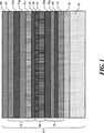
次に図1を見ると、本発明の1つの実施形態によるタンデム式白色発光OLED10の画素の断面図が示されている。OLED装置10は、基板20と、アノード30及びカソード90である離間した2つの電極と、電極間に配置される少なくとも2つのエレクトロルミネッセンスユニット70及び75と、隣接するエレクトロルミネッセンスユニット70及び75間に配置される中間接続層80とを含む。ハットワー(Hatwar)らは、上記で引用した米国特許出願第11/393,767号において、この配置の多数のエレクトロルミネッセンスユニットの使用を記載している。各エレクトロルミネッセンスユニットは、少なくとも1つの正孔輸送層(例えば、正孔輸送層40及び45)を含む。また、アノード30に最も近いエレクトロルミネッセンスユニット70は、正孔注入層35を含み得る。また、カソード90に最も近いエレクトロルミネッセンスユニット75は、電子輸送層55を含み得る。各エレクトロルミネッセンスユニットは、少なくとも1つの有機発光層を含む。エレクトロルミネッセンスユニット70及び75はそれぞれ、異なる発光スペクトルを生じるが、それはこの発明に要求されない。この実施形態において、エレクトロルミネッセンスユニット70は、青色発光化合物を含む青色発光層50bと、黄色発光化合物を含む黄色発光層50yとを含む。本明細書で使用される場合、「黄色発光化合物」という用語は、黄色領域〜赤色領域(すなわち、570nm〜700nm)に主要な発光を有する物質のことを言う。この実施形態において、エレクトロルミネッセンスユニット75は、緑色発光化合物を含み且つ緑色発光を生じる緑色発光層51gと、赤色発光化合物を含み且つ赤色発光を生じる赤色発光層51rと、青色発光化合物を含み且つ青色発光を生じる青色発光層51bとを含む。本明細書に記載されている発明は、この発光層の組合せに限定されず、当業者に知られているように、多くの異なる発光層及び発光層の組合せが使用され得る。
Turning now to FIG. 1, a cross-sectional view of a pixel of a tandem white
タンデム式OLED装置10は、隣接するエレクトロルミネッセンスユニット70及び75間に配置される中間接続層80をさらに含む。中間接続層80は、隣接するエレクトロルミネッセンスユニットに効果的なキャリア注入を与える。金属、金属化合物又は他の無機化合物がキャリア注入に効果的である。しかしながら、これらの材料はしばしば、低抵抗率を有し、それらは60oo0であることができ、画素クロストークをもたらす。また、中間接続層80を構成する層の光透過性は、エレクトロルミネッセンスユニットに生じる放射を装置に放出することができるようにできるだけ高くすべきである。したがって、中間接続層80中で主に有機物質を使用することがしばしば好ましい。中間接続層80は、n−ドープ有機層95と、電子受容層38とを含む。電子受容層38は、n−ドープ有機層95よりもカソードに近接して配置される。
The
中間接続層80において、n−ドープ有機層95は、アルカリ金属及び有機アルカリ金属錯体を含む。有機アルカリ金属錯体のアルカリ金属は、周期表の第1族に属する。これらの中でも、リチウムが最も好ましい。この発明に有用な有機アルカリ金属錯体は、式A:
A (Li+)m(Q)n
(式中、Qはアニオン性有機配位子であり、m及びnは、錯体に中性電荷を与えるように独立的に選択された整数である。)による有機リチウム化合物を含む。
In the
A (Li + ) m (Q) n
(Wherein Q is an anionic organic ligand and m and n are integers independently selected to give a neutral charge to the complex).
アニオン性有機配位子Qは、最も適切にはモノアニオン性であり、酸素、窒素又は炭素からなる少なくとも1つのイオン性部分を含有する。酸素を含有するエノラート又は他の互変異性系の場合、それは酸素に結合したリチウムと見なされて描かれるが、リチウムは他の部分に結合してキレートを形成してもよい。また、配位子は、リチウムと配位結合又は供与結合を形成し得る少なくとも1つの窒素原子を含有することが望ましい。整数m及びnは1超過であることができ、それはクラスター錯体を形成するためのいくつかの有機リチウム化合物についての公知の傾向を示す。 The anionic organic ligand Q is most suitably monoanionic and contains at least one ionic moiety consisting of oxygen, nitrogen or carbon. In the case of an enolate containing oxygen or other tautomeric system, it is depicted as lithium bound to oxygen, but lithium may bind to other moieties to form chelates. In addition, the ligand preferably contains at least one nitrogen atom that can form a coordination bond or a donor bond with lithium. The integers m and n can be greater than 1, which indicates a known trend for some organolithium compounds to form cluster complexes.
他の実施形態において、式Bは、有機アルカリ金属錯体を表す。 In other embodiments, Formula B represents an organoalkali metal complex.
式中、Z及び破線は、2〜4個の原子を表し、且つリチウムカチオンと共に5〜7員環を完成するのに必要な結合を表し、
各Aは水素又は置換基を表し、各Bは水素、又はZ原子上の独立して選択された置換基を表し、ただし、2つ以上の置換基は結合して縮合環又は縮合環系を形成することができ、
jは0〜3であり、kは1又は2であり、
m及びnは、錯体に中性電荷を与えるように独立して選択された整数である。
Wherein Z and the dashed line represent 2-4 atoms and represent the bonds necessary to complete a 5-7 membered ring with the lithium cation,
Each A represents hydrogen or a substituent, and each B represents hydrogen or an independently selected substituent on the Z atom, provided that two or more substituents are joined to form a fused ring or fused ring system. Can be formed,
j is 0-3, k is 1 or 2,
m and n are integers independently selected to give a neutral charge to the complex.
式Bの化合物の中でも、置換基A及びBが一緒になって追加の環系(additional ringsystem)を形成することが最も望ましい。この追加の環系は、追加のヘテロ原子をさらに含有してリチウムと配位結合又は供与結合する多座配位子を形成し得る。望ましいヘテロ原子は、窒素又は酸素である。式Bの有用な化合物は、米国特許出願公開第2006/086405号においてベグレイ(Begley)によって記載されており、その開示は参照することによって本明細書中に援用される。式Bにおいて、示された酸素は、ヒドロキシル基、カルボキシル基又はケト基の一部であることが好ましい。適切な窒素配位子の例は、8−ヒドロキシキノリン、2−ヒドロキシメチルピリジン、ピペコリン酸、又はピリジンカルボン酸である。 Of the compounds of formula B, it is most desirable that the substituents A and B together form an additional ring system. This additional ring system may further contain additional heteroatoms to form multidentate ligands that coordinate or donate to lithium. Desirable heteroatoms are nitrogen or oxygen. Useful compounds of formula B are described by Begley in US Patent Application Publication No. 2006/086405, the disclosure of which is hereby incorporated by reference. In formula B, the oxygen shown is preferably part of a hydroxyl group, a carboxyl group or a keto group. Examples of suitable nitrogen ligands are 8-hydroxyquinoline, 2-hydroxymethylpyridine, pipecolic acid, or pyridinecarboxylic acid.
有用な有機アルカリ金属錯体の具体例は以下の通りである。 Specific examples of useful organic alkali metal complexes are as follows.
上記のうち特に有用なものは、フェナントロリン誘導体(例えば、C1及び関連錯体)である。他の例は、ベグレイによって記載されている。 Particularly useful among the above are phenanthroline derivatives (eg, C1 and related complexes). Another example is described by Begley.
n−ドープ有機層95中のアルカリ金属は、好ましくはリチウムである。Li金属の濃度は、ホスト材料組成物の0.1〜5体積%であり、好ましくは0.5〜2体積%の範囲内である。 The alkali metal in the n-doped organic layer 95 is preferably lithium. The concentration of Li metal is 0.1 to 5% by volume of the host material composition, and preferably 0.5 to 2% by volume.
いくつかの実施形態において、n−ドープ有機層95は、非荷電(uncharged)フェナントロリン誘導体をさらに含み得る。かかるフェナントロリン誘導体は、電子輸送層に有用であるとして公知である。有用な非荷電フェナントロリン誘導体は、バソフェン又はBphenとしても知られている4,7−ジフェニル−1,10−フェナントロリンである。 In some embodiments, the n-doped organic layer 95 can further include an uncharged phenanthroline derivative. Such phenanthroline derivatives are known to be useful for electron transport layers. A useful uncharged phenanthroline derivative is 4,7-diphenyl-1,10-phenanthroline, also known as bathophen or Bphen.
電子受容層38は、無機化合物(例えば、金属酸化物、金属窒化物、金属炭化物、金属イオンと有機配位子との錯体、遷移金属イオンと有機配位子との錯体)を含み得る。電子受容層38に使用するのに適切な物質としては、米国特許第6,208,075号に記載されているようなプラズマ蒸着フルオロカーボンポリマー(CFx)、米国特許第6,720,573B2号及び米国特許公開第2004/113547A1号に記載されているような強力な酸化剤(例えば、ヘキサアザトリフェニレン誘導体(構造D))、又は他の強力な酸化剤(例えば、F4TCNQのような有機物、又は酸化モリブデン、FeCl3若しくはFeF3のような無機物)が挙げられ得る。電子受容物質としても知られる他の有用な酸化剤は、リヤオらによる同一出願人の米国特許第11/867,707号に記載されており、その開示は、参照することによって本明細書中に援用される。 The electron-accepting layer 38 may include an inorganic compound (for example, a metal oxide, a metal nitride, a metal carbide, a complex of a metal ion and an organic ligand, or a complex of a transition metal ion and an organic ligand). Suitable materials for use in the electron-accepting layer 38 include plasma deposited fluorocarbon polymers (CFx) as described in US Pat. No. 6,208,075, US Pat. No. 6,720,573 B2, and US Strong oxidants (eg, hexaazatriphenylene derivatives (Structure D)) as described in Patent Publication No. 2004 / 113547A1, or other strong oxidants (eg, organics such as F 4 TCNQ, or And inorganic substances such as molybdenum oxide, FeCl 3 or FeF 3 ). Other useful oxidants, also known as electron acceptors, are described in commonly assigned US Pat. No. 11 / 867,707 by Riao et al., The disclosure of which is hereby incorporated by reference. Incorporated.
この目的のために有用なヘキサアザトリフェニレン誘導体は、次の構造を有するヘキサシアノヘキサアザトリフェニレンである。 A useful hexaazatriphenylene derivative for this purpose is hexacyanohexaazatriphenylene having the following structure:
また、必要ではないが、電子受容層38は、2つの成分(例えば、ジピラジノ[2,3−f:2’,3’−h]キノザリンヘキサカルボニトリル、F4TCNQ又はFeCl3などの強力な酸化剤をドープした、アミン化合物などの上記有機物質の1つ)から構成され得る。 Also, although not required, the electron-accepting layer 38 has two components (eg, dipyrazino [2,3-f: 2 ′, 3′-h] quinosalinehexacarbonitrile, F 4 TCNQ, or FeCl 3 ). One of the above organic substances, such as amine compounds, doped with a strong oxidant.
OLED装置は、支持基板、例えば、OLED基板20上に一般に形成される。基板と接する電極は、便宜上、下部電極と呼ばれる。基板20は、発光の意図する方向に応じ、光透過性であっても不透明であってもよい。光透過特性は、基板を通してEL発光を見るのに好ましい。透明なガラス又はプラスチックは、このような場合に一般に使用される。EL発光が上部電極を通して見られる応用に関しては、下部支持体の透過特性は重要ではないため、光透過性、光吸収性又は光反射性であり得る。この場合において使用される基板としては、ガラス、プラスチック、半導体材料、シリコン、セラミックス、及び回路基板材料が挙げられるが、これらに限定されない。もちろん、これらの装置構成においては、光透過性上部電極を与える必要がある。
The OLED device is generally formed on a support substrate, for example, the
アノード30は、基板20の上方に形成される。EL発光がアノードを通して見られるなら、興味のある発光のために、アノードは透明又はほぼ透明でなければならない。本発明に使用される共通の透明アノード物質は、インジウムスズ酸化物(ITO)、インジウム亜鉛酸化物(IZO)及びスズ酸化物であるが、他の金属酸化物(アルミニウム−又はインジウム−ドープ亜鉛酸化物、マグネシウム−インジウム酸化物及びニッケル−タングステン酸化物が挙げられるが、これらに限定されない)が働き得る。これらの酸化物に加えて、金属窒化物(例えば、窒化ガリウム)、金属セレン化物(例えば、セレン化亜鉛)、及び金属硫化物(例えば、硫化亜鉛)が、アノードとして使用され得る。EL発光がカソード電極を通してのみ見られる応用に関しては、アノードの透過特性は重要ではなく、透明、不透明又は反射性(reflective)であるかに関らず、多くの導電性物質が使用され得る。本発明のための導電性物質(conductor)の例としては、金、銀、イリジウム、モリブデン、パラジウム、及び白金が挙げられるが、これらに限定されない。透過性又は他の場合の典型的なアノード物質は、4.0eV以上の仕事関数を有する。所望のアノード物質は、蒸発、スパッタリング、化学気相蒸着、又は電気化学析出などの任意の適切な方法によって堆積され得る。必要なら、アノード物質は、公知のフォトリソグラフィープロセスを用いてパターン化され得る。
The
カソード90は、他のOLED層の上方に形成される。装置が表面発光(トップエミッション)であるなら、電極は、透明又はほぼ透明でなければならない。かかる応用に関して、金属は、薄く(好ましくは25nm未満)なければならないか、又は透明な導電性酸化物(例えば、インジウムスズ酸化物、インジウム亜鉛酸化物)若しくはこれらの物質の組み合わせを使用しなければならない。任意に透明なカソードは、米国特許第5,776,623号に、より詳細に記載されている。装置が底面発光(ボトムエミッション)であるなら、カソードは、アルミニウム、モリブデン、金、イリジウム、銀、マグネシウム、上記の透明な導電性酸化物、又はこれらの組み合わせなどの金属を含む、OLED装置に有用であると知られている任意の導電性物質であり得る。所望の物質は、低電圧で電子注入を促進し、効果的な安定性を有する。有用なカソード物質は、低仕事関数金属(<4.0eV)又は金属合金をしばしば含有する。蒸発、スパッタリング又は化学気相蒸着によってカソード物質を堆積させることができる。必要なら、多くの公知の方法(米国特許第5,276,380号及び欧州特許第0732868号に記載されているようなスルーマスク堆積(through-mask deposition)、集積シャドーマスク(integral shadow masking)、レーザーアブレーション、及び選択化学気相蒸着が挙げられるが、これらに限定されない)を通じてパターニングが達成され得る。
The
正孔注入層35は、有機物質又は無機物質の単一又は混合物から形成され得る。正孔注入層は、いくつかの層に分けることができ、各層は、同一又は異なる物質のいずれかから構成される。正孔注入物質は、それに続く有機層の膜形成特性を改善するため、及び正孔輸送層への正孔の注入を容易にするために役立ち得る。正孔注入層に使用するのに適切な物質は、電子不足物質(米国特許第4,720,432号に記載されているようなポルフィリン及びフタロシアニン化合物、ホスファゼン化合物、従来の正孔輸送層物質よりも強い電子ドナーである特定の芳香族アミン化合物(例えば、N,N,N,N−テトラアリールベンジジン化合物)が挙げられるが、これらに限定されない)である。他の有用な実施形態において、正孔注入層としては、欧州特許第0891121A1号及び欧州特許第1029909A1号に教示されているようなパラ−フェニレンジアミン、ジヒドロフェナジン、2,6−ジアミノナフタレン、2,6−ジアミノアントラセン、2,6,9,10−テトラアミノアントラセン、アニリノエチレン、N,N,N,N−テトラアリールベンジジン、モノ若しくはポリアミノ化ペリレン、モノ若しくはポリアミノ化コロネン、ポリアミノ化ピレン、モノ若しくはポリアミノ化フルオランテン、モノ若しくはポリアミノ化クリセン、モノ若しくはポリアミノ化アントラセン、モノ若しくはポリアミノ化トリフェニレン、又はモノ若しくはポリアミノ化テトラセン部分を組み込んだ化合物が挙げられ、さらに、第2物質が、N,N,N,N−テトラアリールベンジジン又はN−アリールカルバゾール部分のいずれかを含有するアミン化合物を含む。
The
正孔注入層35は、金属酸化物、金属窒化物、金属炭化物、金属イオンと有機配位子との錯体、及び遷移金属イオンと有意配位子との錯体などの無機化合物を含み得る。
The
また、正孔注入層に使用するのに適切な物質としては、米国特許第6,208,075号に記載されているようなプラズマ蒸着フルオロカーボンポリマー(CFx)、米国特許第6,720,573B2号及び米国特許公開第2004/113547A1号に記載されているような強力な酸化剤(例えば、ヘキサアザトリフェニレン誘導体(上記の構造D))、又は他の強力な酸化剤(例えば、F4TCNQのような有機物、又は酸化モリブデン、FeCl3若しくはFeF3のような無機物)が挙げられ得る。この目的のために有用なヘキサアザトリフェニレン誘導体は、ヘキサシアノヘキサアザトリフェニレン(上記の構造E)である。 Also suitable materials for use in the hole injection layer include plasma deposited fluorocarbon polymers (CFx) as described in US Pat. No. 6,208,075, US Pat. No. 6,720,573 B2. And strong oxidants such as those described in U.S. Patent Publication No. 2004 / 113547A1, such as hexaazatriphenylene derivatives (Structure D above), or other strong oxidants such as F 4 TCNQ Organic materials, or inorganic materials such as molybdenum oxide, FeCl 3 or FeF 3 ). A useful hexaazatriphenylene derivative for this purpose is hexacyanohexaazatriphenylene (structure E above).
また、必要ではないが、正孔注入層は、2つの成分(例えば、ジピラジノ[2,3−f:2’,3’−h]キノザリンヘキサカルボニトリル、F4TCNQ又はFeCl3などの強力な酸化剤をドープした、アミン化合物などの上記有機物質の1つ)から構成され得る。 Also, although not required, the hole injection layer may be composed of two components (eg, dipyrazino [2,3-f: 2 ′, 3′-h] quinosalinehexacarbonitrile, F 4 TCNQ or FeCl 3 ). One of the above organic substances, such as amine compounds, doped with a strong oxidant.
正孔輸送層40は、OLED装置に有用な任意の正孔輸送物質を含むことができ、その多くの例は当業者に公知である。所望の正孔輸送物質は、蒸発、スパッタリング、化学気相蒸着、電気化学プロセス、ドナー物質からの熱転写(thermal transfer)又はレーザー熱転写などの任意の適切な方法によって堆積され得る。正孔輸送層に有用な正孔輸送物質は、芳香族第3級アミンなどの化合物を含むことが公知であり、芳香族第3級アミンは、炭素原子のみに結合した少なくとも1つの3価窒素原子を含有し、その少なくとも1つが芳香環の一部である化合物であると理解される。1つの形態において、芳香族第3級アミンは、モノアリールアミン、ジアリールアミン、トリアリールアミン、又はポリマーアリールアミン(polymeric arylamine)などのアリールアミンであり得る。典型的なモノマートリアリールアミン(monomeric triarylamine)は、米国特許第3,180,730号においてクルプフェル(Klupfel)らによって説明されている。1つ以上のビニル基で置換された、及び/又は少なくとも1つの活性水素含有基を含む他の適切なトリアリールアミンは、米国特許第3,567,450号及び同第3,658,520号においてブラントレイ(Brantley)らによって開示されている。
The
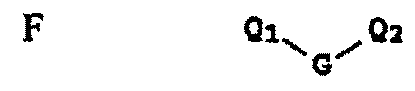
芳香族第3級アミンのより好ましい類は、米国特許第4,720,432号及び同第5,061,569号に記載されているような、少なくとも2つの芳香族第3級アミン部分を含むものである。かかる化合物としては、構造式Fによって表されるものが挙げられる。 A more preferred class of aromatic tertiary amines contain at least two aromatic tertiary amine moieties as described in US Pat. Nos. 4,720,432 and 5,061,569. It is a waste. Such compounds include those represented by Structural Formula F.
![]()
![]()
式中、Q1及びQ2は、独立して選択された芳香族第3級アミン部分であり、Gは、炭素−炭素結合のアリーレン、シクロアルキレン又はアルキレン基などの結合基である。 Where Q 1 and Q 2 are independently selected aromatic tertiary amine moieties and G is a linking group such as an arylene, cycloalkylene or alkylene group of carbon-carbon bonds.
かかる芳香族第3級アミンの1つの類は、テトラアリールジアミンである。所望のテトラアリールジアミンは、アリーレン基を介して結合した2つのジアリールアミノ基を含む。有用なテトラアリールジアミンとしては、式Gによって表されるものが挙げられる。 One class of such aromatic tertiary amines are tetraaryldiamines. The desired tetraaryldiamine contains two diarylamino groups linked via an arylene group. Useful tetraaryldiamines include those represented by Formula G.
式中、各Areは、フェニレン又はアントラセン部分などの、独立して選択されたアリーレン基であり、nは1〜4の整数であり、Ar、R7、R8及びR9は、独立して選択されたアリール基である。 Wherein each Are is an independently selected arylene group, such as a phenylene or anthracene moiety, n is an integer from 1 to 4, and Ar, R 7 , R 8 and R 9 are independently The selected aryl group.
上記の構造式F及びGの様々なアルキル、アルキレン、アリール及びアリーレン部分は、それぞれ順に置換され得る。典型的な置換基としては、アルキル基、アルコキシ基、アリール基、アリールオキシ基、並びにフッ化物、塩化物及び臭化物などのハロゲンが挙げられる。様々なアルキル及びアルキレン部分は、1〜6個の炭素原子を典型的に含有する。シクロアルキル部分は、3〜10個の炭素原子を含有し得るが、5個、6個又は7個の炭素原子(例えば、シクロペンチル、シクロヘキシル及びシクロヘプチル環構造)を典型的に含有する。アリール及びアリーレン部分は、通常、フェニル及びフェニレン部分である。有用には、正孔輸送ホスト物質は、N,N,N’,N’−テトラアリールベンジジンであり、式GのAreがフェニレン基を表し、nが2であるものである。 The various alkyl, alkylene, aryl and arylene moieties of structural formulas F and G above can each be substituted in turn. Typical substituents include alkyl groups, alkoxy groups, aryl groups, aryloxy groups, and halogens such as fluoride, chloride and bromide. The various alkyl and alkylene moieties typically contain 1 to 6 carbon atoms. Cycloalkyl moieties can contain from 3 to 10 carbon atoms, but typically contain 5, 6 or 7 carbon atoms (eg, cyclopentyl, cyclohexyl and cycloheptyl ring structures). The aryl and arylene moieties are usually phenyl and phenylene moieties. Usefully, the hole transporting host material is N, N, N ', N'-tetraarylbenzidine, where Are of formula G represents a phenylene group and n is 2.
電子輸送層55は、OLED装置に有用な任意の電子輸送物質を含むことができ、その多くの例は当業者に公知である。電子輸送層55は、オキシン自体(8−キノリノール又は8−ヒドロキシキノリンとも一般に称される)のキレートを含む、1つ以上の金属キレートオキシノイド化合物を含有し得る。かかる化合物は、電子の注入及び輸送を促し、高水準の性能を示し、薄膜の形状に容易に製造される。典型的な意図するオキシノイド化合物は、構造式Hを満足するものである。
The
式中、Mは金属を表し、nは1〜3の整数であり、それぞれ存在するZは、少なくとも2つの縮合芳香環を有する核(nucleus)を完成する原子を独立して表す。 In the formula, M represents a metal, n is an integer of 1 to 3, and each Z present independently represents an atom that completes a nucleus having at least two fused aromatic rings.
上記から、金属は、1価、2価又は3価の金属であり得ることが明らかである。金属は、例えば、リチウム、ナトリウム若しくはカリウムなどのアルカリ金属;マグネシウム若しくはカルシウムなどのアルカリ土類金属;又はホウ素若しくはアルミニウムなどの土類金属であり得る。一般に、有用なキレート金属(chelating metal)であると知られている任意の1価、2価又は3価の金属が使用され得る。 From the above it is clear that the metal can be a monovalent, divalent or trivalent metal. The metal can be, for example, an alkali metal such as lithium, sodium or potassium; an alkaline earth metal such as magnesium or calcium; or an earth metal such as boron or aluminum. In general, any monovalent, divalent or trivalent metal known to be a useful chelating metal can be used.
Zは、少なくとも2つの縮合芳香環を含有する複素環を完成し、その少なくとも1つはアゾール又はアジン環である。もし必要なら、脂肪族環及び芳香環の両方を含む追加の環が、2つの要求される環と縮合され得る。機能を改善することなしの分子バルク(molecular bulk)の増加を避けるために、環原子の数は、通常18以下に保持される。 Z completes a heterocycle containing at least two fused aromatic rings, at least one of which is an azole or azine ring. If necessary, additional rings, including both aliphatic and aromatic rings, can be fused with the two required rings. In order to avoid an increase in molecular bulk without improving function, the number of ring atoms is usually kept below 18.
有用なキレートオキシノイド化合物の例は以下の通りである。
CO−1:アルミニウムトリソキシン[別名:トリス(8−キノリノラト)アルミニウム(III)]、
CO−2:マグネシウムビオキシン[別名:ビス(8−キノリノラト)マグネシウム(II)]、
CO−3:ビス[ベンゾ{f}−8−キノリノラト]亜鉛(II)、
CO−4:ビス(2−メチル−8−キノリノラト)アルミニウム(III)−μ−オキソ−ビス(2−メチル−8−キノリノラト)アルミニウム(III)、
CO−5:インジウムトリソキシン[別名:トリス(8−キノリノラト)インジウム]、
CO−6:アルミニウムトリス(5−メチルオキシン)[別名:トリス(5−メチル−8−キノリノラト)アルミニウム(III)]、
CO−7:リチウムオキシン[別名:(8−キノリノラト)リチウム(I)]、
CO−8:ガリウムオキシン[別名:トリス(8−キノリノラト)ガリウム(III)]、及び
CO−9:ジルコニウムオキシン[別名:テトラ(8−キノリノラト)ジルコニウム(IV)]
Examples of useful chelating oxinoid compounds are as follows.
CO-1: aluminum trisoxin [alias: tris (8-quinolinolato) aluminum (III)],
CO-2: magnesium bioxin [alias: bis (8-quinolinolato) magnesium (II)],
CO-3: bis [benzo {f} -8-quinolinolato] zinc (II),
CO-4: bis (2-methyl-8-quinolinolato) aluminum (III) -μ-oxo-bis (2-methyl-8-quinolinolato) aluminum (III),
CO-5: indium trisoxin [alias: tris (8-quinolinolato) indium],
CO-6: aluminum tris (5-methyloxine) [alias: tris (5-methyl-8-quinolinolato) aluminum (III)],
CO-7: lithium oxine [alias: (8-quinolinolato) lithium (I)],
CO-8: gallium oxine [alias: tris (8-quinolinolato) gallium (III)], and CO-9: zirconium oxine [aka: tetra (8-quinolinolato) zirconium (IV)]
他の電子輸送物質としては、米国特許第4,356,429号に開示されている様々なブタジエン誘導体や、米国特許第4,539,507号に記載されている様々な複素環式光学的光沢剤が挙げられる。ベンズアゾール、オキサジアゾール、トリアゾール、ピリジンチアジアゾール、トリアジン、フェナントロリン誘導体、及びいくつかのシロール誘導体もまた、有用な電子輸送物質である。電子輸送物質として有用であることが知られている置換1,10−フェナントロリン化合物は、特開2003−115387号公報、特開2004−311184号公報、特開2001−267080号公報、及び国際公開第2002/043449号に開示されている。 Other electron transport materials include various butadiene derivatives disclosed in US Pat. No. 4,356,429, and various heterocyclic optical glosses described in US Pat. No. 4,539,507. Agents. Benzazoles, oxadiazoles, triazoles, pyridine thiadiazoles, triazines, phenanthroline derivatives, and some silole derivatives are also useful electron transport materials. Substituted 1,10-phenanthroline compounds known to be useful as electron transport materials are disclosed in JP-A No. 2003-115387, JP-A No. 2004-311184, JP-A No. 2001-267080, and International Publication No. It is disclosed in 2002/043449.
本明細書に示される実施形態は、4つの有機発光層:青色発光層50b及び51b、黄色発光層50y、緑色発光層51g及び赤色発光層51rを含む。しかしながら、この発明は、この配置に限定されない。多種多様な発光層が当該技術分野において公知であり、この発明において使用され得る。かかる発光層としては、赤色発光層、黄色発光層、緑色発光層、青色発光層、又はこれらの組合せが挙げられ得る。本明細書に記載されたもののような発光層は、電子−正孔再結合に応じて光を生じる。蒸発、スパッタリング、化学気相蒸着、電気化学析出、又はドナー物質からの放射熱転写(radiation thermal transfer)などの任意の適切な方法によって、所望の有機発光物質を堆積させ得る。この発明の発光層は、1つ以上の発光ゲスト化合物をドープした1つ以上のホスト物質、又は発光がドーパントから主にもたらされるドーパントを含む。ドーパントは、特定のスペクトルを有する色彩光(color light)を生じ、且つ他の所望の特性を有するように選択される。ドーパントは、0.01〜15重量%でホスト物質中に典型的に塗装される。
The embodiment shown herein includes four organic light emitting layers: blue
発光層は、アントラセンホスト、望ましくは9,10−ジアリールアントラセンを含むことができ、その特定の誘導体(式I)は、エレクトロルミネッセンスを支持し得る有用なホスト物質群を構成することが知られており、400nmより長い波長の発光(例えば、青色、緑色、黄色、橙色又は赤色)に特に適している。 The emissive layer can comprise an anthracene host, preferably 9,10-diarylanthracene, and certain derivatives thereof (formula I) are known to constitute useful host materials that can support electroluminescence. And is particularly suitable for light emission longer than 400 nm (eg, blue, green, yellow, orange or red).
式中、R1、R2、R3及びR4は、各環における1つ以上の置換基を表し、各置換基は下記の群からそれぞれ選択される。
第1群:水素、又は1〜24個の炭素原子を有するアルキル
第2群:5〜20個の炭素原子を有するアリール又は置換アリール
第3群:アントラセニル、ピレニル又はペリレニルの縮合芳香環を完成するのに必要な4〜24個の炭素原子
第4群:フリル、チエニル、ピリジル、キノリニル又は他の複素環系の縮合芳香族複素環を完成するのに必要な5〜24個の炭素原子を有するヘテロアリール又は置換ヘテロアリール
第5群:1〜24個の炭素原子を有するアルコキシルアミノ、アルキルアミノ又はアリールアミノ
第6群:フッ素又はシアノ
In the formula, R 1 , R 2 , R 3 and R 4 represent one or more substituents in each ring, and each substituent is selected from the following group.
Group 1: Hydrogen or alkyl having 1 to 24 carbon atoms Group 2: Aryl or substituted aryl having 5 to 20 carbon atoms Group 3: Complete anthracenyl, pyrenyl or perylenyl fused aromatic ring From 4 to 24 carbon atoms required to form a fourth group: 5 to 24 carbon atoms required to complete a fused aromatic heterocycle of furyl, thienyl, pyridyl, quinolinyl or other heterocyclic ring system Heteroaryl or substituted heteroaryl Group 5: alkoxylamino, alkylamino or arylamino having 1 to 24 carbon atoms Group 6: fluorine or cyano
特に有用なのは、R1及びR2、並びにいくつかの場合においてR3及びR4が追加の芳香環を表す化合物である。 Particularly useful are compounds in which R 1 and R 2 and in some cases R 3 and R 4 represent an additional aromatic ring.
ホスト又は共同ホスト(co-host)物質として有用なのは、芳香族第3級アミン(例えば、上記の構造F及びG)などの特定の正孔輸送物質、及びキレート化されたオキシノイド化合物(例えば、上記の構造H)などの特定の電子輸送物質である。 Useful as host or co-host materials are certain hole transport materials such as aromatic tertiary amines (eg, structures F and G above), and chelated oxinoid compounds (eg, Specific electron transport materials such as structure H).
上記のホスト物質に加えて、発光層はまた、第1発光物質として1つ以上のドーパントを含む。赤色発光ドーパントは、以下の構造Jのジインデノペリレン化合物を含み得る。 In addition to the host material described above, the light emitting layer also includes one or more dopants as the first light emitting material. The red light emitting dopant may comprise a diindenoperylene compound of structure J below.
式中、X1−X16は、水素、又は1〜24個の炭素原子を有するアルキル基、5〜20個の炭素原子を有するアリール又は置換アリール基、1つ以上の縮合芳香環又は環系を完成する、4〜24個の炭素原子を含有する炭化水素基、若しくはハロゲンなどの置換基から独立して選択され、ただし、置換基は560nm〜640nmの最大発光を与えるように選択される。 Wherein X 1 -X 16 is hydrogen or an alkyl group having 1 to 24 carbon atoms, an aryl or substituted aryl group having 5 to 20 carbon atoms, one or more fused aromatic rings or ring systems Is independently selected from a hydrocarbon group containing 4 to 24 carbon atoms, or a substituent such as halogen, provided that the substituent is selected to give a maximum emission of 560 nm to 640 nm.
ハットワー(Hatwar)らは、米国特許第7,247,394号において(その内容は参照することによって本明細書に援用される)、この種類の有用な赤色ドーパントについての説明に役立つ実例を示す。 Hatwar et al. In US Pat. No. 7,247,394, the contents of which are hereby incorporated by reference, provide an illustrative example of this type of useful red dopant.
いくつかの他の赤色ドーパントは、式Kによって表される染料のDCM類(DCM class)に属する。 Some other red dopants belong to the DCMs of the dyes represented by formula K (DCM class).
式中、Y1−Y5は、水素(hydro)、アルキル、置換アルキル、アリール、又は置換アリールから独立して選択される1つ以上の基を表し;Y1−Y5は、アクリル基を独立して含むか、又は一対で結合して(joined pairwise)1つ以上の縮合環を形成することができ;ただし、Y3及びY5は一緒になって縮合環を形成しない。リックス(Ricks)らは、米国特許第7,252,893号において(その内容は参照することによって本明細書に援用される)、DCM類の特に有用なドーパントの構造を示す。 Wherein, Y 1 -Y 5 are hydrogen (hydro), alkyl, substituted alkyl, aryl, or independently from substituted aryl and represents one or more groups selected; Y 1 -Y 5 are acrylic group They can be included independently or joined pairwise to form one or more fused rings; provided that Y 3 and Y 5 are not taken together to form a fused ring. Ricks et al. In US Pat. No. 7,252,893, the contents of which are hereby incorporated by reference, show the structure of particularly useful dopants for DCMs.
黄色発光ドーパントは、以下の構造の化合物を含み得る。 The yellow light-emitting dopant may include a compound having the following structure:
式中、A1−A6及びA’1−A’6は、各環における1つ以上の置換基を表し、各置換基は、以下の群の1つから個別に選択される。
第1群:水素、又は1〜24個の炭素原子を有するアルキル
第2群:5〜20個の炭素原子を有するアリール又は置換アリール
第3群:縮合芳香環又は環系を完成する、4〜24個の炭素原子を含有する炭化水素
第4群:単結合を介して結合されるか、又は縮合芳香族複素環を完成する、チアゾリル、フリル、チエニル、ピリジル、キノリニル又は他の複素環系などの5〜24個の炭素原子を有するヘテロアリール又は置換へテロアリール
第5群:1〜24個の炭素原子を有するアルコキシルアミノ、アルキルアミノ又はアリールアミノ
第6群:フルオロ又はシアノ
Wherein A 1 -A 6 and A ′ 1 -A ′ 6 represent one or more substituents in each ring, each substituent being individually selected from one of the following groups:
Group 1: hydrogen or alkyl having 1 to 24 carbon atoms Group 2: aryl or substituted aryl having 5 to 20 carbon atoms Group 3: completing a fused aromatic ring or ring system 4 to Hydrocarbons containing 24 carbon atoms Group 4: Thiazolyl, furyl, thienyl, pyridyl, quinolinyl or other heterocycles linked via a single bond or completing a fused aromatic heterocycle A heteroaryl or substituted heteroaryl having from 5 to 24 carbon atoms, Group 5: alkoxylamino, alkylamino or arylamino having from 1 to 24 carbon atoms Group 6: fluoro or cyano
特に有用な黄色ドーパントの例は、米国特許第7,252,893号においてリックス(Ricks)らにより示されている。 An example of a particularly useful yellow dopant is shown by Ricks et al. In US Pat. No. 7,252,893.
緑色発光ドーパントは、キナクリドン化合物、例えば、以下の構造の化合物を含み得る。 The green light emitting dopant may include a quinacridone compound, for example, a compound having the following structure:
式中、置換基R1及びR2は独立して、アルキル、アルコキシル、アリール又はヘテロアリールであり;置換基R3〜R12は独立して、水素、アルキル、アルコキシル、ハロゲン、アリール、又はヘテロアリールであり、隣接した置換基R3〜R10は任意に接続されて、縮合芳香環及び縮合芳香族複素環などの1つ以上の環系(ring systems)を形成することができ、ただし、置換基は510nm〜540nmの最大発光を与えるように選択される。アルキル、アルコキシル、アリール、ヘテロアリール、縮合芳香環及び縮合芳香族複素環置換基は、さらに置換され得る。有用なキナクリドンのいくつかの例としては、米国特許第5,593,788号及び米国特許出願公開第2004/0001969A1に開示されているものが挙げられる。有用なキナクリドン緑色ドーパントの例としては、以下のものが挙げられる。 In which the substituents R 1 and R 2 are independently alkyl, alkoxyl, aryl or heteroaryl; the substituents R 3 to R 12 are independently hydrogen, alkyl, alkoxyl, halogen, aryl or hetero Aryl, adjacent substituents R 3 to R 10 can be optionally connected to form one or more ring systems such as fused aromatic rings and fused aromatic heterocycles, provided that The substituent is selected to give a maximum emission between 510 nm and 540 nm. Alkyl, alkoxyl, aryl, heteroaryl, fused aromatic ring and fused aromatic heterocyclic substituents may be further substituted. Some examples of useful quinacridones include those disclosed in US Pat. No. 5,593,788 and US Patent Application Publication No. 2004 / 0001969A1. Examples of useful quinacridone green dopants include:
また、緑色発光ドーパントは、以下の式によって表されるような、2,6−ジアミノアントラセン発光ドーパントを含み得る。 The green luminescent dopant may also include a 2,6-diaminoanthracene luminescent dopant, as represented by the following formula:
青色発光ドーパントは、構造Pのビス(アジニル)アゼンボロン錯体化合物を含み得る。 The blue emitting dopant may comprise a bis (azinyl) azembolone complex compound of structure P.
式中、A及びA’は、少なくとも1つの窒素を含有する6員芳香環系に相当する独立したアジン環系を表し;(Xa)n及び(Xb)mは、1つ以上の独立して選択された置換基を表し、且つアクリル置換基を含むか、又は結合してA又はA1と縮合した環を形成し;m及びnは独立して0〜4であり;Za及びZbは、独立して選択された置換基であり;1、2、3、4、1’、2’、3’及び4’は、炭素又は窒素原子のいずれかとして独立的に選択され;ただし、Xa、Xb、Za及びZb、1、2、3、4、1’、2’、3’及び4’は、青色発光を与えるように選択される。 Wherein A and A ′ represent an independent azine ring system corresponding to a 6-membered aromatic ring system containing at least one nitrogen; (X a ) n and (X b ) m are one or more independent Represents a selected substituent and includes or is bonded to an acrylic substituent to form a fused ring with A or A 1 ; m and n are independently 0-4; Z a and Z b is an independently selected substituent; 1, 2, 3, 4, 1 ′, 2 ′, 3 ′ and 4 ′ are independently selected as either a carbon or nitrogen atom; However, X a , X b , Z a and Z b , 1, 2, 3, 4, 1 ′, 2 ′, 3 ′ and 4 ′ are selected to give blue light emission.
リックス(Ricks)らは、上記類のドーパントのいくつかの例を開示する。発光層におけるこの類のドーパントの濃度は、望ましくは0.1%〜5%である。 Ricks et al. Disclose some examples of the above class of dopants. The concentration of this type of dopant in the light emitting layer is desirably between 0.1% and 5%.
他の類の青色ドーパントは、ペリレン類である。ペリレン類の特に有用な青色ドーパントは、ペリレン及びテトラ−t−ブチルペリレン(TBP)を含む。 Another class of blue dopants are perylenes. Particularly useful blue dopants of perylenes include perylene and tetra-t-butylperylene (TBP).
他の類の青色ドーパントとしては、米国特許第5,121,029号及び米国特許出願公開第2006/0093856号においてヘルバー(Helber)らによって記載された化合物を含む、ジスチリルベンゼン、スチリルビフェニル、及びジスチリルビフェニルなどのスチリルアレンやジスチリルアレンの青色発光誘導体が挙げられる。青色発光を与えるこれらの誘導体の中でも、第2発光層52において特に有用なのは、ジアリールアミノ基で置換されたものであり、本明細書ではアミノスチリルアレンドーパントと称する。例としては、以下に示される一般構造Q1のビス[2−[4−[N,N−ジアリールアミノ]フェニル]ビニル]−ベンゼン: Other classes of blue dopants include distyrylbenzene, styrylbiphenyl, and the compounds described by Helber et al. In US Pat. No. 5,121,029 and US Patent Publication No. 2006/0093856, and And blue light-emitting derivatives of styryl allene such as distyryl biphenyl and distyryl allene. Among these derivatives that give blue light emission, those particularly useful in the second light-emitting layer 52 are those substituted with a diarylamino group, and are referred to herein as aminostyryl allene dopants. Examples include bis [2- [4- [N, N-diarylamino] phenyl] vinyl] -benzene of general structure Q1 shown below:
以下に示される一般構造Q2の[N,N−ジアリールアミノ][2−[4−[N,N−ジアリールアミノ]フェニル]ビニル]ビフェニル: [N, N-diarylamino] [2- [4- [N, N-diarylamino] phenyl] vinyl] biphenyl of general structure Q2 shown below:
及び以下に示される一般構造Q3のビス[2−[4−[N,N−ジアリールアミノ]フェニル]ビニル]ビフェニル: And bis [2- [4- [N, N-diarylamino] phenyl] vinyl] biphenyl of general structure Q3 shown below:
が挙げられる。 Is mentioned.
式Q1〜Q3において、X1−X4は同一でも異なっていてもよく、アルキル、アリール、縮合アリール、ハロ(halo)、又はシアノなどの1つ以上の置換基をそれぞれ表す。好ましい実施形態において、X1−X4はそれぞれ、1〜10個の炭素原子をそれぞれ含有するアルキル基である。リックス(Ricks)らは、米国特許第7,252,893号において、この類の特に好ましい青色ドーパントを開示する。 In formulas Q1-Q3, X 1 -X 4 may be the same or different and each represents one or more substituents such as alkyl, aryl, fused aryl, halo, or cyano. In preferred embodiments, X 1 -X 4 are each an alkyl group each containing 1 to 10 carbon atoms. Ricks et al. In US Pat. No. 7,252,893 discloses a particularly preferred blue dopant of this class.
さらに、OLED装置10は、他の層を含み得る。例えば、アルカリ金属若しくはアルカリ土類金属、アルカリハロゲン化物塩、又はアルカリ金属若しくはアルカリ土類金属ドープ有機層などの電子注入層もまた、カソード90と電子輸送層55との間に存在し得る。
Further, the
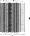
次に図2を見ると、本発明に従う他の実施形態のタンデム式OLED装置15の断面図が示されている。この実施形態において、中間接続層85は、n−ドープ層95と接触し且つカソード90よりもアノード30に近接する非ドープ層65をさらに含む。非ドープ層65は、芳香族炭化水素誘導体、望ましくは構造Iのために上記したようなアントラセン誘導体を含む。また、非ドープ層65は、構造Aのために上記したような有機アルカリ金属錯体を含み得る。非ドープ層65に有用な有機アルカリ金属錯体の例は、ヒドロキノリンの塩、例えば、8−キノリノラトリチウムである。
Turning now to FIG. 2, a cross-sectional view of another embodiment tandem OLED device 15 according to the present invention is shown. In this embodiment, the intermediate connection layer 85 further includes an
本発明及びその利益が、以下の比較例によって、より良く理解され得る。実施例3〜6は本発明の代表例であるが、実施例1及び2は、比較目的の独創性のないタンデム式OLEDの例である。真空蒸着されるとされる層は、約10-6Torrの真空下で加熱ボートからの蒸発によって蒸着させた。OLED層の蒸着の後、カプセル化のために各装置をドライボックスに移した。OLEDは、10mm2の発光領域を有する。装置は、電極間に20mA/cm2の電流を適用することによって試験した。実施例1〜6の結果を表1に与える。 The invention and its benefits can be better understood by the following comparative examples. Examples 3-6 are representative examples of the present invention, while Examples 1 and 2 are examples of non-creative tandem OLEDs for comparison purposes. The layer to be vacuum deposited was deposited by evaporation from a heated boat under a vacuum of about 10 −6 Torr. After deposition of the OLED layer, each device was transferred to a dry box for encapsulation. The OLED has a light emitting area of 10 mm 2 . The device was tested by applying a current of 20 mA / cm 2 between the electrodes. The results of Examples 1-6 are given in Table 1.
<実施例1(比較)>
1.きれいなガラス基板にインジウムスズ酸化物(ITO)をスパッタリングにより堆積させ、60nmの厚さの透明電極を形成した。
2.上記で調製したITO表面を酸素プラズマエッチングで処理した。
3.上記で調製した基板を、正孔注入層(HIL)としてヘキサシアノヘキサアザトリフェニレン(CHATP)の10nm層を真空蒸着することによってさらに処理した。
<Example 1 (comparison)>
1. Indium tin oxide (ITO) was deposited on a clean glass substrate by sputtering to form a transparent electrode having a thickness of 60 nm.
2. The ITO surface prepared above was treated with oxygen plasma etching.
3. The substrate prepared above was further processed by vacuum depositing a 10 nm layer of hexacyanohexaazatriphenylene (CHATP) as a hole injection layer (HIL).
4.上記で調製した基板を、正孔輸送層(HTL)として4,4’−ビス[N−(1−ナフチル)−N−フェニルアミノ]ビフェニル(NPB)の150nm層を真空蒸着することによってさらに処理した。
5.上記で調製した基板を、48%のNPB(ホストとして)、48%の9−(1−ナフチル)−10−(2−ナフチル)アントラセン(NNA)(共同ホストとして)、4%の黄色発光ドーパントであるジフェニルテトラ−t−ブチルルブレン(PTBR)含む20nmの黄色発光層を真空蒸着することによってさらに処理した。
4). The substrate prepared above is further processed by vacuum deposition of a 150 nm layer of 4,4′-bis [N- (1-naphthyl) -N-phenylamino] biphenyl (NPB) as a hole transport layer (HTL). did.
5. 48% NPB (as host), 48% 9- (1-naphthyl) -10- (2-naphthyl) anthracene (NNA) (as co-host), 4% yellow
6.上記で調製した基板を、91%のNNAホスト、8%のNPB共同ホスト、青色発光ドーパントとして1%のBEPを含む30nmの青色発光層を真空蒸着することによってさらに処理した。 6). The substrate prepared above was further processed by vacuum deposition of a 30 nm blue light emitting layer containing 91% NNA host, 8% NPB co-host, and 1% BEP as a blue light emitting dopant.
7.49%の4,7−ジフェニル−1,10−フェナントロリン(バソフェン又はBphenとしても知られている)、共同ホストとして49%のトリス(8−キノリノラト)アルミニウム(III)(ALQ)、2%のLi金属を含む40nmのnドープ有機層を真空蒸着した。
8.上記で調製した基板を、電子受容層としてCHATPの10nm層を真空蒸着することによってさらに処理した。
9.上記で調製した基板を、正孔輸送層(HTL)としてNPBの10nm層を真空蒸着することによってさらに処理した。
10.上記で調製した基板を、94.5%のNPB、黄色発光ドーパントとして5%のPTBR、及び赤色発光ドーパントとして0.5%のジベンゾ{[f,f’]−4,4’,7,7’−テトラフェニル]ジインデノ−[1,2,3−cd:1’,2’,3’−lm]ペリレン(TPDBP)を含む20nmの赤色発光層を真空蒸着することによってさらに処理した。
7.49% 4,7-diphenyl-1,10-phenanthroline (also known as bathophen or Bphen), 49% tris (8-quinolinolato) aluminum (III) (ALQ), 2% as co-host A 40 nm n-doped organic layer containing a Li metal was vacuum deposited.
8). The substrate prepared above was further processed by vacuum depositing a 10 nm layer of CHATP as the electron accepting layer.
9. The substrate prepared above was further processed by vacuum depositing a 10 nm layer of NPB as a hole transport layer (HTL).
10. The substrate prepared above was 94.5% NPB, 5% PTBR as a yellow luminescent dopant, and 0.5% dibenzo {[f, f ′]-4,4 ′, 7,7 as a red luminescent dopant. Further processing was carried out by vacuum deposition of a 20 nm red light emitting layer containing '-tetraphenyl] diindeno- [1,2,3-cd: 1', 2 ', 3'-lm] perylene (TPDBP).
11.上記で調製した基板を、84.4%の2−フェニル−9,10−ビス(2−ナフチル)アントラセン(PBNA)、15%のNPB、緑色発光ドーパントとして0.6%のジフェニルキナクリドン(DPQ)を含む15nmの緑色発光層を真空蒸着することによってさらに処理した。
12.上記で調製した基板を、99%のPBNA、青色発光ドーパントとして1%のBEPを含む20nmの青色発光層を真空蒸着することによってさらに処理した。
13.共同ホストとして49%のBphen及び49%のALQ、2%のLi金属を含む35nmの混合電子輸送層を真空蒸着した。
14.基板上に100nmのアルミニウム層を蒸発によって堆積させ、カソード層を形成した。
11. The substrate prepared above was converted to 84.4% 2-phenyl-9,10-bis (2-naphthyl) anthracene (PBNA), 15% NPB, 0.6% diphenylquinacridone (DPQ) as a green emitting dopant. Further processing was carried out by vacuum deposition of a 15 nm green emitting layer containing.
12 The substrate prepared above was further processed by vacuum deposition of a 20 nm blue light emitting layer containing 99% PBNA and 1% BEP as a blue light emitting dopant.
13. A 35 nm mixed electron transport layer containing 49% Bphen and 49% ALQ, 2% Li metal as co-host was vacuum deposited.
14 A 100 nm aluminum layer was deposited on the substrate by evaporation to form a cathode layer.
<実施例2(比較)>
工程7を以下のようにしたこと以外は、実施例1で上記した通りにしてOLED装置を作製した。
7.ホストとして98%のBphen、2%のLi金属を含む40nmのnドープ有機層を真空蒸着した。
<Example 2 (comparison)>
An OLED device was fabricated as described in Example 1 except that Step 7 was as follows.
7). A 40 nm n-doped organic layer containing 98% Bphen and 2% Li metal as a host was vacuum deposited.
<実施例3(発明品)>
工程7を以下のようにしたこと以外は、実施例1で上記した通りにしてOLED装置を作製した。
7.ホストとして98%の2−(2−ヒドロキシフェニル)−1,10−フェナントロリンのリチウム塩(Li−HPP)、2%のLi金属を含む40nmのnドープ有機層を真空蒸着した。
<Example 3 (Invention)>
An OLED device was fabricated as described in Example 1 except that Step 7 was as follows.
7). A 40 nm n-doped organic layer containing 98% lithium salt of 2- (2-hydroxyphenyl) -1,10-phenanthroline (Li-HPP) and 2% Li metal as a host was vacuum deposited.
<実施例4(発明品)>
工程7を以下のようにしたこと以外は、実施例1で上記した通りにしてOLED装置を作製した。
7.49%のLi−HPP、共同ホストとして49%のALQ、2%のLi金属を含む40nmのnドープ有機層を真空蒸着した。
<Example 4 (Invention)>
An OLED device was fabricated as described in Example 1 except that Step 7 was as follows.
A 40 nm n-doped organic layer containing 7.49% Li-HPP, 49% ALQ as co-host, 2% Li metal was vacuum deposited.
<実施例5(発明品)>
以下の工程6aを工程6の後に加え、工程7を以下のようにしたこと以外は、実施例1で上記した通りにしてOLED装置を作製した。
6a.上記で調製した基板を、30nmのPBNAの非ドープ層を真空蒸着することによってさらに処理した。
7.ホストとして98%のLi−HPP、2%のLi金属を含む10nmのnドープ有機層を真空蒸着した。
<Example 5 (Invention)>
The following step 6a was added after step 6 and an OLED device was fabricated as described in Example 1 except that step 7 was as follows.
6a. The substrate prepared above was further processed by vacuum deposition of an undoped layer of 30 nm PBNA.
7). A 10 nm n-doped organic layer containing 98% Li-HPP as a host and 2% Li metal was vacuum deposited.
<実施例6(発明品)>
以下の工程6aを工程6の後に加え、工程7を以下のようにしたこと以外は、実施例1で上記した通りにしてOLED装置を作製した。
6a.上記で調製した基板を、50%のPBNA及び50%の8−キノリノラトリチウム(LiQ)の20nmの非ドープ層を真空蒸着することによってさらに処理した。
7.ホストとして98%のLi−HPP、2%のLi金属を含む20nmのnドープ有機層を真空蒸着した。
<Example 6 (Invention)>
The following step 6a was added after step 6 and an OLED device was fabricated as described in Example 1 except that step 7 was as follows.
6a. The substrate prepared above was further processed by vacuum deposition of a 20 nm undoped layer of 50% PBNA and 50% 8-quinolinolatolithium (LiQ).
7). A 20 nm n-doped organic layer containing 98% Li-HPP and 2% Li metal as a host was vacuum deposited.
これらの実施例を試験した結果を以下の表1に示す。 The results of testing these examples are shown in Table 1 below.
本発明の実施例は、それらの各々の比較例と比較して、改善された輝度、発光効率、及びルーメン/ワット(lumens/watt)を示す。また、ほとんどが改善された駆動電圧を示し、いくつかが改善された電力効率及び量子効率を示す。 The examples of the present invention show improved brightness, luminous efficiency, and lumens / watt compared to their respective comparative examples. Also, most show improved drive voltage and some show improved power efficiency and quantum efficiency.
10 OLED装置
15 OLED装置
20 基板
30 アノード
35 正孔注入層
38 電子受容層
40 正孔輸送層
45 正孔輸送層
50y 黄色発光層
50b 青色発光層
51r 赤色発光層
51g 緑色発光層
51b 青色発光層
55 電子輸送層
65 非ドープ層
70 ルミネッセンスユニット
75 ルミネッセンスユニット
80 中間接続層
85 中間接続層
90 カソード
95 nドープ有機層
10 OLED device 15
Claims (10)
(b)カソードと、
(c)前記アノードと前記カソードとの間に配置される少なくとも2つのエレクトロルミネッセンスユニットであって、各エレクトロルミネッセンスユニットが、少なくとも1つの正孔輸送層及び1つの有機発光層を含むエレクトロルミネッセンスユニットと、
(d)隣接するエレクトロルミネッセンスユニットの間に配置される中間接続層であって、前記中間接続層がn−ドープ有機層及び電子受容層を含み、前記電子受容層がn−ドープ有機層よりも前記カソードに近接して配置され、前記n−ドープ有機層がアルカリ金属及び有機アルカリ金属錯体を含み、且つ前記中間接続層が、前記アノードに近接する側に前記n−ドープ層と接触する非ドープ層をさらに含む中間接続層と
を含むタンデム式OLED装置。(A) an anode;
(B) a cathode;
(C) at least two electroluminescent units disposed between the anode and the cathode, each electroluminescent unit comprising at least one hole transport layer and one organic light emitting layer; ,
(D) An intermediate connection layer disposed between adjacent electroluminescence units, the intermediate connection layer including an n-doped organic layer and an electron accepting layer, wherein the electron accepting layer is more than the n-doped organic layer. being disposed close to the cathode, said n- doped organic layer is observed containing an alkali metal and an organic alkali metal complex, and the intermediate connector is in contact with said n- doped layer on the side close to the anode non A tandem OLED device including an intermediate connection layer further including a doped layer .
Applications Claiming Priority (3)
| Application Number | Priority Date | Filing Date | Title |
|---|---|---|---|
| US12/022,427 | 2008-01-30 | ||
| US12/022,427 US7955719B2 (en) | 2008-01-30 | 2008-01-30 | Tandem OLED device with intermediate connector |
| PCT/US2009/000292 WO2009097084A1 (en) | 2008-01-30 | 2009-01-19 | Tandem oled device with intermediate connector |
Publications (3)
| Publication Number | Publication Date |
|---|---|
| JP2011511414A JP2011511414A (en) | 2011-04-07 |
| JP2011511414A5 JP2011511414A5 (en) | 2012-09-27 |
| JP5113913B2 true JP5113913B2 (en) | 2013-01-09 |
Family
ID=40548857
Family Applications (1)
| Application Number | Title | Priority Date | Filing Date |
|---|---|---|---|
| JP2010544995A Active JP5113913B2 (en) | 2008-01-30 | 2009-01-19 | Tandem OLED device with intermediate connection layer |
Country Status (7)
| Country | Link |
|---|---|
| US (1) | US7955719B2 (en) |
| EP (1) | EP2243176B1 (en) |
| JP (1) | JP5113913B2 (en) |
| KR (1) | KR101225674B1 (en) |
| CN (1) | CN101960632B (en) |
| AT (1) | ATE521997T1 (en) |
| WO (1) | WO2009097084A1 (en) |
Families Citing this family (31)
| Publication number | Priority date | Publication date | Assignee | Title |
|---|---|---|---|---|
| US8115382B2 (en) * | 2007-09-20 | 2012-02-14 | Semiconductor Energy Laboratory Co., Ltd. | Light-emitting element, light-emitting device, and electronic device, comprising controlled carrier transport |
| CN102067730A (en) * | 2008-05-16 | 2011-05-18 | Lg化学株式会社 | Stacked organic light-emitting diode |
| WO2010062643A1 (en) * | 2008-10-28 | 2010-06-03 | The Regents Of The University Of Michigan | Stacked white oled having separate red, green and blue sub-elements |
| KR100994118B1 (en) * | 2009-01-13 | 2010-11-15 | 삼성모바일디스플레이주식회사 | Organic light emitting diode and manufacturing method thereof |
| JP2010225563A (en) * | 2009-03-25 | 2010-10-07 | Panasonic Electric Works Co Ltd | Organic el element |
| KR20120083215A (en) | 2009-06-05 | 2012-07-25 | 베이징 비젼녹스 테크놀로지 컴퍼니 리미티드 | Organic electroluminescent device and testing method thereof |
| KR101411122B1 (en) * | 2009-11-13 | 2014-06-25 | 베이징 비젼녹스 테크놀로지 컴퍼니 리미티드 | Organic material and organic EL device using the same material |
| JP5573127B2 (en) * | 2009-11-27 | 2014-08-20 | セイコーエプソン株式会社 | LIGHT EMITTING ELEMENT, DISPLAY DEVICE, AND ELECTRONIC DEVICE |
| WO2011161424A1 (en) | 2010-06-25 | 2011-12-29 | Cambridge Display Technology Limited | Organic light-emitting device and method |
| US8633475B2 (en) * | 2010-07-16 | 2014-01-21 | Idemitsu Kosan Co., Ltd. | Organic electroluminescence device and a method for producing the device |
| US8637858B2 (en) | 2010-09-24 | 2014-01-28 | Novaled Ag | Tandem white OLED |
| JP2012186091A (en) * | 2011-03-07 | 2012-09-27 | Seiko Epson Corp | Light-emitting element, light-emitting device, display device, and electronic apparatus |
| EP2503616A1 (en) | 2011-03-21 | 2012-09-26 | Polyphotonix Limited | Emissive element for light emitting device, light emitting device and method for manufacturing such element and device |
| DE112012001477B4 (en) | 2011-03-31 | 2018-04-05 | Panasonic Intellectual Property Management Co., Ltd. | Organic electroluminescent element |
| DE102011117357A1 (en) * | 2011-10-29 | 2013-05-02 | Karlsruher Institut für Technologie | Preparing solution of n-doped organic low molecular semiconductor comprises dissolving organic semiconductor in aprotic solvent, adding alkali metal, and optionally separating/purifying semiconductor solution under inert gas atmosphere |
| KR101429924B1 (en) | 2011-12-08 | 2014-08-14 | 엘지디스플레이 주식회사 | Tandem White Organic Emitting Device |
| KR102089331B1 (en) * | 2012-12-28 | 2020-03-16 | 엘지디스플레이 주식회사 | Organic light emitting display |
| DE102013114047B4 (en) * | 2012-12-28 | 2016-09-01 | Lg Display Co., Ltd. | Organic light-emitting display devices |
| CN103972421A (en) * | 2013-01-31 | 2014-08-06 | 海洋王照明科技股份有限公司 | Organic light-emitting device and production method thereof |
| CN104051636A (en) * | 2013-03-11 | 2014-09-17 | 海洋王照明科技股份有限公司 | Organic light-emitting device and preparation method thereof |
| KR102077141B1 (en) * | 2013-05-29 | 2020-02-14 | 삼성디스플레이 주식회사 | Organic light emitting device |
| KR102200388B1 (en) | 2014-06-23 | 2021-01-07 | 엘지디스플레이 주식회사 | White organic light emitting device |
| CN107112418B (en) | 2014-08-01 | 2021-01-15 | 正交公司 | Photolithographic patterning of organic electronic devices |
| EP3175497A4 (en) | 2014-08-01 | 2018-11-21 | Orthogonal Inc. | Photolithographic patterning of devices |
| JP6792547B2 (en) | 2014-08-01 | 2020-11-25 | オーソゴナル,インコーポレイテッド | Photolithography patterning method for devices |
| JP6653315B2 (en) | 2014-08-01 | 2020-02-26 | オーソゴナル,インコーポレイテッド | Photolithographic patterning of organic electronic devices |
| US10236466B2 (en) | 2014-11-14 | 2019-03-19 | Nanyang Technological University | Organic light emitting device |
| KR102311911B1 (en) * | 2014-11-25 | 2021-10-13 | 엘지디스플레이 주식회사 | Organic Light Emitting Device and Organic Light Emitting Display Device using the same |
| CN104795432A (en) * | 2015-05-04 | 2015-07-22 | 京东方科技集团股份有限公司 | Organic light-emitting diode device and display device |
| KR102143726B1 (en) * | 2016-07-27 | 2020-08-11 | 후지필름 가부시키가이샤 | Photoelectric conversion element, imaging element, optical sensor, compound |
| CN113287369B (en) * | 2019-01-15 | 2024-09-13 | 索尼半导体解决方案公司 | Display device, method of manufacturing display device, and electronic apparatus |
Family Cites Families (24)
| Publication number | Priority date | Publication date | Assignee | Title |
|---|---|---|---|---|
| US4885211A (en) | 1987-02-11 | 1989-12-05 | Eastman Kodak Company | Electroluminescent device with improved cathode |
| US4769292A (en) | 1987-03-02 | 1988-09-06 | Eastman Kodak Company | Electroluminescent device with modified thin film luminescent zone |
| JP3451680B2 (en) | 1993-11-15 | 2003-09-29 | 三菱化学株式会社 | Organic electroluminescent device |
| US5683823A (en) | 1996-01-26 | 1997-11-04 | Eastman Kodak Company | White light-emitting organic electroluminescent devices |
| US6337492B1 (en) | 1997-07-11 | 2002-01-08 | Emagin Corporation | Serially-connected organic light emitting diode stack having conductors sandwiching each light emitting layer |
| JP3884564B2 (en) | 1998-05-20 | 2007-02-21 | 出光興産株式会社 | Organic EL light emitting device and light emitting device using the same |
| JP4611578B2 (en) | 2001-07-26 | 2011-01-12 | 淳二 城戸 | Organic electroluminescent device |
| US6872472B2 (en) * | 2002-02-15 | 2005-03-29 | Eastman Kodak Company | Providing an organic electroluminescent device having stacked electroluminescent units |
| JP3933591B2 (en) | 2002-03-26 | 2007-06-20 | 淳二 城戸 | Organic electroluminescent device |
| US6717358B1 (en) | 2002-10-09 | 2004-04-06 | Eastman Kodak Company | Cascaded organic electroluminescent devices with improved voltage stability |
| US6936961B2 (en) * | 2003-05-13 | 2005-08-30 | Eastman Kodak Company | Cascaded organic electroluminescent device having connecting units with N-type and P-type organic layers |
| DE102004002587B4 (en) * | 2004-01-16 | 2006-06-01 | Novaled Gmbh | Image element for an active matrix display |
| US20060289882A1 (en) * | 2004-07-30 | 2006-12-28 | Kazuki Nishimura | Organic electroluminescent element and organic electroluminescent display device |
| JP4578215B2 (en) * | 2004-11-30 | 2010-11-10 | 三洋電機株式会社 | Organic electroluminescent device and organic electroluminescent display device |
| US7273663B2 (en) * | 2004-08-20 | 2007-09-25 | Eastman Kodak Company | White OLED having multiple white electroluminescence units |
| US7075231B1 (en) * | 2005-01-03 | 2006-07-11 | Eastman Kodak Company | Tandem OLEDs having low drive voltage |
| US7494722B2 (en) * | 2005-02-23 | 2009-02-24 | Eastman Kodak Company | Tandem OLED having an organic intermediate connector |
| KR100696693B1 (en) * | 2005-04-13 | 2007-03-20 | 삼성에스디아이 주식회사 | Organic light emitting diode display |
| US20060240277A1 (en) * | 2005-04-20 | 2006-10-26 | Eastman Kodak Company | Tandem OLED device |
| US20060286405A1 (en) | 2005-06-17 | 2006-12-21 | Eastman Kodak Company | Organic element for low voltage electroluminescent devices |
| US7531959B2 (en) * | 2005-06-29 | 2009-05-12 | Eastman Kodak Company | White light tandem OLED display with filters |
| JP4837958B2 (en) * | 2005-08-26 | 2011-12-14 | 大日本印刷株式会社 | Organic electroluminescence device |
| US20070046189A1 (en) * | 2005-08-31 | 2007-03-01 | Eastman Kodak Company | Intermediate connector for a tandem OLED device |
| US7332860B2 (en) * | 2006-03-30 | 2008-02-19 | Eastman Kodak Company | Efficient white-light OLED display with filters |
-
2008
- 2008-01-30 US US12/022,427 patent/US7955719B2/en active Active
-
2009
- 2009-01-19 KR KR1020107018500A patent/KR101225674B1/en active IP Right Grant
- 2009-01-19 CN CN200980107862.1A patent/CN101960632B/en active Active
- 2009-01-19 EP EP09705020A patent/EP2243176B1/en active Active
- 2009-01-19 JP JP2010544995A patent/JP5113913B2/en active Active
- 2009-01-19 AT AT09705020T patent/ATE521997T1/en not_active IP Right Cessation
- 2009-01-19 WO PCT/US2009/000292 patent/WO2009097084A1/en active Application Filing
Also Published As
| Publication number | Publication date |
|---|---|
| WO2009097084A1 (en) | 2009-08-06 |
| KR20100129279A (en) | 2010-12-08 |
| US7955719B2 (en) | 2011-06-07 |
| EP2243176B1 (en) | 2011-08-24 |
| ATE521997T1 (en) | 2011-09-15 |
| US20090191428A1 (en) | 2009-07-30 |
| KR101225674B1 (en) | 2013-01-23 |
| CN101960632B (en) | 2012-06-27 |
| CN101960632A (en) | 2011-01-26 |
| JP2011511414A (en) | 2011-04-07 |
| EP2243176A1 (en) | 2010-10-27 |
Similar Documents
| Publication | Publication Date | Title |
|---|---|---|
| JP5113913B2 (en) | Tandem OLED device with intermediate connection layer | |
| JP5133974B2 (en) | Efficient white light OLED display with filter | |
| KR101405278B1 (en) | High-performance tandem white oled | |
| JP5606921B2 (en) | White OLED with blue light emitting layer | |
| US7273663B2 (en) | White OLED having multiple white electroluminescence units | |
| US7821201B2 (en) | Tandem OLED device with intermediate connector | |
| US7560862B2 (en) | White OLEDs with a color-compensated electroluminescent unit | |
| KR101595433B1 (en) | Tandem white oled with efficient electron transfer | |
| KR101225673B1 (en) | High-color-temperature tandem white oled | |
| KR101457576B1 (en) | Stabilized White-Emitting OLED Device | |
| EP2183799B1 (en) | High-performance broadband oled device |
Legal Events
| Date | Code | Title | Description |
|---|---|---|---|
| A621 | Written request for application examination |
Free format text: JAPANESE INTERMEDIATE CODE: A621 Effective date: 20110803 |
|
| A521 | Request for written amendment filed |
Free format text: JAPANESE INTERMEDIATE CODE: A523 Effective date: 20120807 |
|
| A871 | Explanation of circumstances concerning accelerated examination |
Free format text: JAPANESE INTERMEDIATE CODE: A871 Effective date: 20120807 |
|
| TRDD | Decision of grant or rejection written | ||
| A975 | Report on accelerated examination |
Free format text: JAPANESE INTERMEDIATE CODE: A971005 Effective date: 20121003 |
|
| A01 | Written decision to grant a patent or to grant a registration (utility model) |
Free format text: JAPANESE INTERMEDIATE CODE: A01 Effective date: 20121009 |
|
| A01 | Written decision to grant a patent or to grant a registration (utility model) |
Free format text: JAPANESE INTERMEDIATE CODE: A01 |
|
| A61 | First payment of annual fees (during grant procedure) |
Free format text: JAPANESE INTERMEDIATE CODE: A61 Effective date: 20121012 |
|
| FPAY | Renewal fee payment (event date is renewal date of database) |
Free format text: PAYMENT UNTIL: 20151019 Year of fee payment: 3 |
|
| R150 | Certificate of patent or registration of utility model |
Ref document number: 5113913 Country of ref document: JP Free format text: JAPANESE INTERMEDIATE CODE: R150 Free format text: JAPANESE INTERMEDIATE CODE: R150 |
|
| R250 | Receipt of annual fees |
Free format text: JAPANESE INTERMEDIATE CODE: R250 |
|
| R250 | Receipt of annual fees |
Free format text: JAPANESE INTERMEDIATE CODE: R250 |
|
| R250 | Receipt of annual fees |
Free format text: JAPANESE INTERMEDIATE CODE: R250 |
|
| R250 | Receipt of annual fees |
Free format text: JAPANESE INTERMEDIATE CODE: R250 |
|
| R250 | Receipt of annual fees |
Free format text: JAPANESE INTERMEDIATE CODE: R250 |
|
| R250 | Receipt of annual fees |
Free format text: JAPANESE INTERMEDIATE CODE: R250 |
|
| R250 | Receipt of annual fees |
Free format text: JAPANESE INTERMEDIATE CODE: R250 |
|
| R250 | Receipt of annual fees |
Free format text: JAPANESE INTERMEDIATE CODE: R250 |
|
| R250 | Receipt of annual fees |
Free format text: JAPANESE INTERMEDIATE CODE: R250 |