JP5113349B2 - Rgb熱隔離基板 - Google Patents
Rgb熱隔離基板 Download PDFInfo
- Publication number
- JP5113349B2 JP5113349B2 JP2006150628A JP2006150628A JP5113349B2 JP 5113349 B2 JP5113349 B2 JP 5113349B2 JP 2006150628 A JP2006150628 A JP 2006150628A JP 2006150628 A JP2006150628 A JP 2006150628A JP 5113349 B2 JP5113349 B2 JP 5113349B2
- Authority
- JP
- Japan
- Prior art keywords
- led
- submount
- contact pad
- structure according
- leds
- Prior art date
- Legal status (The legal status is an assumption and is not a legal conclusion. Google has not performed a legal analysis and makes no representation as to the accuracy of the status listed.)
- Active
Links
Images
Classifications
-
- H—ELECTRICITY
- H10—SEMICONDUCTOR DEVICES; ELECTRIC SOLID-STATE DEVICES NOT OTHERWISE PROVIDED FOR
- H10H—INORGANIC LIGHT-EMITTING SEMICONDUCTOR DEVICES HAVING POTENTIAL BARRIERS
- H10H20/00—Individual inorganic light-emitting semiconductor devices having potential barriers, e.g. light-emitting diodes [LED]
- H10H20/80—Constructional details
- H10H20/85—Packages
- H10H20/857—Interconnections, e.g. lead-frames, bond wires or solder balls
-
- H—ELECTRICITY
- H01—ELECTRIC ELEMENTS
- H01L—SEMICONDUCTOR DEVICES NOT COVERED BY CLASS H10
- H01L2224/00—Indexing scheme for arrangements for connecting or disconnecting semiconductor or solid-state bodies and methods related thereto as covered by H01L24/00
- H01L2224/01—Means for bonding being attached to, or being formed on, the surface to be connected, e.g. chip-to-package, die-attach, "first-level" interconnects; Manufacturing methods related thereto
- H01L2224/42—Wire connectors; Manufacturing methods related thereto
- H01L2224/47—Structure, shape, material or disposition of the wire connectors after the connecting process
- H01L2224/48—Structure, shape, material or disposition of the wire connectors after the connecting process of an individual wire connector
- H01L2224/4805—Shape
- H01L2224/4809—Loop shape
- H01L2224/48091—Arched
-
- H—ELECTRICITY
- H01—ELECTRIC ELEMENTS
- H01L—SEMICONDUCTOR DEVICES NOT COVERED BY CLASS H10
- H01L2224/00—Indexing scheme for arrangements for connecting or disconnecting semiconductor or solid-state bodies and methods related thereto as covered by H01L24/00
- H01L2224/01—Means for bonding being attached to, or being formed on, the surface to be connected, e.g. chip-to-package, die-attach, "first-level" interconnects; Manufacturing methods related thereto
- H01L2224/42—Wire connectors; Manufacturing methods related thereto
- H01L2224/47—Structure, shape, material or disposition of the wire connectors after the connecting process
- H01L2224/48—Structure, shape, material or disposition of the wire connectors after the connecting process of an individual wire connector
- H01L2224/481—Disposition
- H01L2224/48151—Connecting between a semiconductor or solid-state body and an item not being a semiconductor or solid-state body, e.g. chip-to-substrate, chip-to-passive
- H01L2224/48221—Connecting between a semiconductor or solid-state body and an item not being a semiconductor or solid-state body, e.g. chip-to-substrate, chip-to-passive the body and the item being stacked
- H01L2224/48225—Connecting between a semiconductor or solid-state body and an item not being a semiconductor or solid-state body, e.g. chip-to-substrate, chip-to-passive the body and the item being stacked the item being non-metallic, e.g. insulating substrate with or without metallisation
- H01L2224/48227—Connecting between a semiconductor or solid-state body and an item not being a semiconductor or solid-state body, e.g. chip-to-substrate, chip-to-passive the body and the item being stacked the item being non-metallic, e.g. insulating substrate with or without metallisation connecting the wire to a bond pad of the item
-
- H—ELECTRICITY
- H01—ELECTRIC ELEMENTS
- H01L—SEMICONDUCTOR DEVICES NOT COVERED BY CLASS H10
- H01L2224/00—Indexing scheme for arrangements for connecting or disconnecting semiconductor or solid-state bodies and methods related thereto as covered by H01L24/00
- H01L2224/73—Means for bonding being of different types provided for in two or more of groups H01L2224/10, H01L2224/18, H01L2224/26, H01L2224/34, H01L2224/42, H01L2224/50, H01L2224/63, H01L2224/71
- H01L2224/732—Location after the connecting process
- H01L2224/73251—Location after the connecting process on different surfaces
- H01L2224/73265—Layer and wire connectors
-
- H—ELECTRICITY
- H01—ELECTRIC ELEMENTS
- H01L—SEMICONDUCTOR DEVICES NOT COVERED BY CLASS H10
- H01L25/00—Assemblies consisting of a plurality of semiconductor or other solid state devices
- H01L25/03—Assemblies consisting of a plurality of semiconductor or other solid state devices all the devices being of a type provided for in a single subclass of subclasses H10B, H10D, H10F, H10H, H10K or H10N, e.g. assemblies of rectifier diodes
- H01L25/04—Assemblies consisting of a plurality of semiconductor or other solid state devices all the devices being of a type provided for in a single subclass of subclasses H10B, H10D, H10F, H10H, H10K or H10N, e.g. assemblies of rectifier diodes the devices not having separate containers
- H01L25/075—Assemblies consisting of a plurality of semiconductor or other solid state devices all the devices being of a type provided for in a single subclass of subclasses H10B, H10D, H10F, H10H, H10K or H10N, e.g. assemblies of rectifier diodes the devices not having separate containers the devices being of a type provided for in group H10H20/00
- H01L25/0753—Assemblies consisting of a plurality of semiconductor or other solid state devices all the devices being of a type provided for in a single subclass of subclasses H10B, H10D, H10F, H10H, H10K or H10N, e.g. assemblies of rectifier diodes the devices not having separate containers the devices being of a type provided for in group H10H20/00 the devices being arranged next to each other
-
- H—ELECTRICITY
- H01—ELECTRIC ELEMENTS
- H01L—SEMICONDUCTOR DEVICES NOT COVERED BY CLASS H10
- H01L2924/00—Indexing scheme for arrangements or methods for connecting or disconnecting semiconductor or solid-state bodies as covered by H01L24/00
- H01L2924/013—Alloys
- H01L2924/0132—Binary Alloys
- H01L2924/01322—Eutectic Alloys, i.e. obtained by a liquid transforming into two solid phases
-
- H—ELECTRICITY
- H01—ELECTRIC ELEMENTS
- H01L—SEMICONDUCTOR DEVICES NOT COVERED BY CLASS H10
- H01L2924/00—Indexing scheme for arrangements or methods for connecting or disconnecting semiconductor or solid-state bodies as covered by H01L24/00
- H01L2924/10—Details of semiconductor or other solid state devices to be connected
- H01L2924/11—Device type
- H01L2924/12—Passive devices, e.g. 2 terminal devices
- H01L2924/1204—Optical Diode
- H01L2924/12041—LED
-
- H—ELECTRICITY
- H10—SEMICONDUCTOR DEVICES; ELECTRIC SOLID-STATE DEVICES NOT OTHERWISE PROVIDED FOR
- H10H—INORGANIC LIGHT-EMITTING SEMICONDUCTOR DEVICES HAVING POTENTIAL BARRIERS
- H10H20/00—Individual inorganic light-emitting semiconductor devices having potential barriers, e.g. light-emitting diodes [LED]
- H10H20/80—Constructional details
- H10H20/85—Packages
- H10H20/8506—Containers
-
- H—ELECTRICITY
- H10—SEMICONDUCTOR DEVICES; ELECTRIC SOLID-STATE DEVICES NOT OTHERWISE PROVIDED FOR
- H10H—INORGANIC LIGHT-EMITTING SEMICONDUCTOR DEVICES HAVING POTENTIAL BARRIERS
- H10H20/00—Individual inorganic light-emitting semiconductor devices having potential barriers, e.g. light-emitting diodes [LED]
- H10H20/80—Constructional details
- H10H20/85—Packages
- H10H20/858—Means for heat extraction or cooling
- H10H20/8582—Means for heat extraction or cooling characterised by their shape
Landscapes
- Led Device Packages (AREA)
- Led Devices (AREA)
Description
一実施形態では、AlInGaPのLEDは、サブマウント内に引っ込んでおり、そのために全てのLEDが同じ光出射平面を有する。
このサブマウントは、黄色、琥珀色、オレンジ色、青緑色のような他の色を発生するLEDに対して使用することもできる。
こういった複数の色のLEDを形成する方法は公知である。LEDの形成の一部の例は、引用により組み込まれている米国特許第6,649,440号、第6,547,249号、第6,274,399号、第6,229,160号、及び第5,233,204号に説明されており、その全ては、「Lumileds Lighting」に譲渡されたものである。
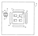
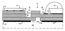
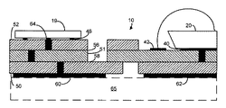
異なる色のLED(例えば、AlInGaN及びAlInGaPのLED)を白色光又は何らかの他の混成色を作り出すために単一モジュールに組み合わせるために、LEDダイは、図1−5に関して説明されるサブマウント10上に装着される。
サブマウント10は、セラミックのような電気絶縁性材料の層で形成される。他の実施形態では、サブマウントは、酸化物の層が電気絶縁性をもたらすシリコンとすることができる。
溝28−31は、構造的一体性を維持するためにAlInGaPのLEDを完全には取り囲まないが、他の実施形態では、溝は、AlInGaPのLEDを完全に取り囲む。
この例においては、AlInGaPのLEDは、フリップチップではなく、上部電極のためのワイヤ接合を必要とする。AlInGaPのLEDのための接触パッド34は、AlInGaPのLEDの底部電極(例えば、n電極)に直接半田付けするための金属(例えば、金)パッド40と、AlInGaPのLEDの上部電極(例えば、p電極)及びパッド42の間のワイヤの接続のための金属パッド42とで構成される。
層50における穴54のパターン(図5にも示す)は、凹部部分26を実質的に取り囲み、LED19の下の層50をLED20の下の層50から熱的に隔離している。
すなわち、溝28−31(図1)及び穴54によって実行される2つのレベルの熱隔離が存在している。溝28−31によって提供される熱隔離が十分である場合は、穴54を削除することができる。
サブマウント10の表面上の金属接点パッドは、セラミック層の間のパターン金属層56及び58に電気的に接続し、これは、次に、サブマウント10の底部上の半田パッド(図5も参照されたい)に接続する。一実施形態では、半田パッド60は、LED19のn又はp電極に電気的に結合し、中心半田パッド62は、下に重なる放熱板への熱伝導のためのみに使用される。
図4は、様々なセラミック層を通って接触パッド、金属層、及び半田パッドを電気的に相互接続する可能なバイア64を示している。バイアの穴は、成形によって形成することができ、スパッタリングを用いて金属で充填される。
1つ又はそれよりも多くのサブマウント10は、他のLEDモジュール及び電源に接続するための金属リードを収容することができるプリント回路基板65(破線の外形で示す)に半田接合することができる。回路基板65は、様々なLEDと直列及び/又は並列に相互接続することができる。回路基板65は、放熱板の目的からアルミ二ウムシートとすることができ、その表面上に薄い電気絶縁層とこの絶縁層の上に金属導体パターンとを有する。回路基板上の対応するパッドに接合されたサブマウントの半田パッドは、アルミ二ウム放熱板への良好な熱経路を提供する。この回路基板は、より大きい放熱板上に装着することができる。
サブマウントは、直接に電源に接続することができるので、回路基板上へのサブマウントの装着は任意的である。
サブマウント10によって提供される熱的分断に加えて、凹部区域26(図1及び図3)が、上部セラミック層52のエッチング又は成形によって設けられる。図示の例においては、AlInGaPのLEDの高さは、GaNのLEDの高さよりも大きいので、凹部26は、サブマウント10上に装着された後に、AlInGaP及びGaNのLEDの上部を実質的に同じ高さにする。このようにして、GaN及びAlInGaPのLEDの光出射平面は同じ高さであり、GaNのLEDの側面から放射された光は、より高いAlInGaPのLEDによって阻止されない。これは、モジュール周囲のより均一な色の光パターンをもたらす。
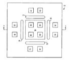
RGBのLED群のアレイを単一のサブマウント上に装着することができる。例えば、各RGB群は、ディスプレイのためのRGBピクセルとして作用することができ、従って、単一サブマウント上のRGB群のアレイは、小さいカラーディスプレイとして作用することができる。このようなサブマウントは、あらゆる大きさとすることができる。サブマウントのアレイは、全ディスプレイのための十分なピクセルを提供し、又は照明のための制御可能カラー光源として作用することができる。
一実施形態では、サブマウントの上部表面積は、6mm2−4cm2の間であり、サブマウント上に装着されるLEDの数に依存する。
凹部部分の位置は、サブマウント上のあらゆる場所とすることができる。また、溝及び穴の配列は、あらゆる適切なパターンとすることができる。サブマウントを利用することができるLEDは、GaP及びGaNのLEDに限定されない。
本発明の特定的な実施形態を示して説明したが、本発明を逸脱することなくそのより広い態様において変更及び修正を行うことができ、従って、特許請求の範囲は、その範囲内に全てのそのような変更及び修正を本発明の真の精神及び範囲に該当するものとして含むことは当業者には明らかであろう。
12、13、14、15、16、17、18、19 LEDGaNのLED
20、21、22、23 AlInGaPのLED
28、29、30、31 溝
Claims (20)
- 発光ダイオード(LED)構造体であって、
電気的に絶縁した本体と、導電体と、少なくとも第1のLEDに接合するための第1の接触パッドと、少なくとも第2のLEDに接合するための第2の接触パッドとを含むサブマウントと、
前記第1の接触パッドに接合した前記第1のLEDと前記第2の接触パッドに接合した前記第2のLEDとの間の熱隔離を高めるために該第1の接触パッドと該第2の接触パッドの間の前記サブマウントにある少なくとも1つの不連続部と、
を含み、
前記サブマウントは、電気絶縁材料の少なくとも第1の層及び第2の層を含み、
前記少なくとも1つの不連続部は、前記第1の層に形成された少なくとも1つの溝を含み、
前記少なくとも1つの不連続部はまた、第2の層に前記少なくとも1つの溝の真下ではない少なくとも1つの不連続部を含む、
ことを特徴とする構造体。 - 前記第1のLEDは、GaPベースのLEDであり、
前記第2のLEDは、GaNベースのLEDである、
ことを特徴とする請求項1に記載の構造体。 - 前記サブマウントは、中央部分及び該中央部分を取り囲む外側部分を有し、
前記第1の接触パッドは、前記中央部分にあり、前記第2の接触パッドは、前記外側部分にあり、前記少なくとも1つの不連続部は、該中央部分と該外側部分の間にある、
ことを特徴とする請求項1に記載の構造体。 - 前記第1の接触パッドを支持する、前記サブマウントの凹部部分を更に含むことを特徴とする請求項1に記載の構造体。
- 前記第2のLEDは、フリップチップであることを特徴とする請求項1に記載の構造体。
- 前記第1のLEDは、ワイヤによって前記第1の接触パッドの1つに接続した1つの電極を有することを特徴とする請求項1に記載の構造体。
- 前記サブマウントは、前記少なくとも2つの層の間に前記導電体を含むことを特徴とする請求項1に記載の構造体。
- 前記導電体は、前記第1の接触パッドと前記第2の接触パッドを相互接続していることを特徴とする請求項7に記載の構造体。
- 複数の組の第1の接触パッドと複数の組の第2の接触パッドがあることを特徴とする請求項1に記載の構造体。
- 前記サブマウントの中央部分に位置する複数の組の第1の接触パッドと該サブマウントの外側部分に位置する複数の組の第2の接触パッドとが存在し、
前記サブマウントにある前記少なくとも1つの不連続部は、前記複数の組の第1の接触パッドと前記複数の組の第2の接触パッドとの間にある、
ことを特徴とする請求項1に記載の構造体。 - 前記サブマウントの前記中央部分は、引っ込んでいることを特徴とする請求項10に記載の構造体。
- 前記第1の表面上の前記第1の接触パッドと前記第2の接触パッドとが前記導電体によって電気的に結合した第3の接触パッドを前記サブマウントの第2の表面上に更に含むことを特徴とする請求項1に記載の構造体。
- 前記電気的に絶縁した本体は、セラミックであることを特徴とする請求項1に記載の構造体。
- 前記第1のLEDは、575nmよりも長い波長を有する光を放射し、前記第2のLEDは、575nmよりも短い波長を有する光を放射することを特徴とする請求項1に記載の構造体。
- 前記第1の表面上に少なくとも第3のLEDに接合するための第3の接触パッドを更に含み、前記第1のLEDは、第1の色の光を放射し、前記第2のLEDは、第2の色の光を放射し、該第3のLEDは、第3の色の光を放射することを特徴とする請求項1に記載の構造体。
- 前記第1の色は、赤色であり、前記第2の色は、青色であり、前記第3の色は、緑色であることを特徴とする請求項15に記載の構造体。
- 前記第1の接触パッドを支持する、前記サブマウントの引っ込んだ部分と、前記第2の接触パッドを支持する引っ込んでいない部分とを更に含み、
前記第1のLEDの上面と前記第2のLEDの上面は、前記サブマウント上に装着された時に実質的に同じ平面にある、
ことを特徴とする請求項1に記載の構造体。 - 前記サブマウントが装着されたプリント回路基板を更に含むことを特徴とする請求項1に記載の構造体。
- 前記サブマウントを収容し、ディスプレイのためのバックライトを形成する反射性筐体を更に含むことを特徴とする請求項1に記載の構造体。
- 前記サブマウントは、回路基板上に装着されるようになっていることを特徴とする請求項1に記載の構造体。
Applications Claiming Priority (2)
| Application Number | Priority Date | Filing Date | Title |
|---|---|---|---|
| US11/118,898 | 2005-04-29 | ||
| US11/118,898 US7952112B2 (en) | 2005-04-29 | 2005-04-29 | RGB thermal isolation substrate |
Publications (2)
| Publication Number | Publication Date |
|---|---|
| JP2006310874A JP2006310874A (ja) | 2006-11-09 |
| JP5113349B2 true JP5113349B2 (ja) | 2013-01-09 |
Family
ID=36604229
Family Applications (1)
| Application Number | Title | Priority Date | Filing Date |
|---|---|---|---|
| JP2006150628A Active JP5113349B2 (ja) | 2005-04-29 | 2006-04-28 | Rgb熱隔離基板 |
Country Status (6)
| Country | Link |
|---|---|
| US (1) | US7952112B2 (ja) |
| EP (1) | EP1878052B1 (ja) |
| JP (1) | JP5113349B2 (ja) |
| CN (1) | CN101171685B (ja) |
| TW (1) | TWI431819B (ja) |
| WO (1) | WO2006117711A1 (ja) |
Families Citing this family (17)
| Publication number | Priority date | Publication date | Assignee | Title |
|---|---|---|---|---|
| KR101240650B1 (ko) * | 2006-01-18 | 2013-03-08 | 삼성디스플레이 주식회사 | 발광 다이오드 모듈, 이를 구비한 백라이트 어셈블리 및이를 구비한 표시 장치 |
| WO2008149267A1 (en) * | 2007-06-06 | 2008-12-11 | Koninklijke Philips Electronics N.V. | Method and apparatus for driving light emitting elements for projection of images |
| JP4996998B2 (ja) * | 2007-07-02 | 2012-08-08 | シャープ株式会社 | 照明装置 |
| JP4969332B2 (ja) * | 2007-06-19 | 2012-07-04 | シャープ株式会社 | 基板及び照明装置 |
| WO2008156020A1 (ja) * | 2007-06-19 | 2008-12-24 | Sharp Kabushiki Kaisha | 基板及び照明装置 |
| JP5536980B2 (ja) * | 2007-11-27 | 2014-07-02 | パナソニック株式会社 | 実装方法 |
| DE102008021014A1 (de) * | 2008-04-25 | 2009-10-29 | Alcan Technology & Management Ag | Vorrichtung mit einer Mehrschichtplatte sowie Licht emittierenden Dioden |
| DE102008021402B4 (de) * | 2008-04-29 | 2023-08-10 | OSRAM Opto Semiconductors Gesellschaft mit beschränkter Haftung | Oberflächenmontierbares Leuchtdioden-Modul und Verfahren zur Herstellung eines oberflächenmontierbaren Leuchtdioden-Moduls |
| JP5503646B2 (ja) | 2008-07-03 | 2014-05-28 | コーニンクレッカ フィリップス エヌ ヴェ | 固体光源のための支持モジュール、このようなモジュールを有する照明装置、及びこのような照明装置を製造するための方法 |
| BRPI1005425B1 (pt) * | 2009-02-05 | 2019-11-05 | Philips Lighting Holding B.V. | dispositivo, sistema e método |
| CN102349353B (zh) | 2009-03-12 | 2016-03-16 | 皇家飞利浦电子股份有限公司 | 具有白炽灯色温性状的led发光设备 |
| CN102639926B (zh) * | 2009-12-02 | 2014-12-24 | 夏普株式会社 | 照明装置和显示装置 |
| US9653643B2 (en) | 2012-04-09 | 2017-05-16 | Cree, Inc. | Wafer level packaging of light emitting diodes (LEDs) |
| US9666764B2 (en) | 2012-04-09 | 2017-05-30 | Cree, Inc. | Wafer level packaging of multiple light emitting diodes (LEDs) on a single carrier die |
| US9142743B2 (en) * | 2011-08-02 | 2015-09-22 | Kabushiki Kaisha Toshiba | High temperature gold-free wafer bonding for light emitting diodes |
| JP6519311B2 (ja) | 2014-06-27 | 2019-05-29 | 日亜化学工業株式会社 | 発光装置 |
| DE102016104202A1 (de) * | 2016-03-08 | 2017-09-14 | Osram Opto Semiconductors Gmbh | Optoelektronisches Halbleiterbauteil |
Family Cites Families (20)
| Publication number | Priority date | Publication date | Assignee | Title |
|---|---|---|---|---|
| US4845405A (en) | 1986-05-14 | 1989-07-04 | Sanyo Electric Co., Ltd. | Monolithic LED display |
| JPS63226080A (ja) | 1987-03-02 | 1988-09-20 | Copal Co Ltd | 発光ダイオ−ド複合組立体 |
| JPH0482036A (ja) * | 1990-07-24 | 1992-03-16 | Fujitsu Ltd | 光ディスクの製造方法および該製造方法に用いる製造装置 |
| US5233204A (en) | 1992-01-10 | 1993-08-03 | Hewlett-Packard Company | Light-emitting diode with a thick transparent layer |
| JPH06270470A (ja) | 1993-03-25 | 1994-09-27 | Sanyo Electric Co Ltd | 光プリントヘッド |
| JP3572924B2 (ja) | 1997-03-06 | 2004-10-06 | 松下電器産業株式会社 | 発光装置及びそれを用いた記録装置 |
| JP3882266B2 (ja) | 1997-05-19 | 2007-02-14 | 日亜化学工業株式会社 | 半導体装置 |
| US6229160B1 (en) | 1997-06-03 | 2001-05-08 | Lumileds Lighting, U.S., Llc | Light extraction from a semiconductor light-emitting device via chip shaping |
| US6194742B1 (en) | 1998-06-05 | 2001-02-27 | Lumileds Lighting, U.S., Llc | Strain engineered and impurity controlled III-V nitride semiconductor films and optoelectronic devices |
| US6133589A (en) | 1999-06-08 | 2000-10-17 | Lumileds Lighting, U.S., Llc | AlGaInN-based LED having thick epitaxial layer for improved light extraction |
| WO2000079605A1 (fr) * | 1999-06-23 | 2000-12-28 | Citizen Electronics Co., Ltd. | Diode électroluminescente |
| US6614103B1 (en) * | 2000-09-01 | 2003-09-02 | General Electric Company | Plastic packaging of LED arrays |
| US6547249B2 (en) | 2001-03-29 | 2003-04-15 | Lumileds Lighting U.S., Llc | Monolithic series/parallel led arrays formed on highly resistive substrates |
| WO2002089221A1 (en) * | 2001-04-23 | 2002-11-07 | Matsushita Electric Works, Ltd. | Light emitting device comprising led chip |
| JP3668438B2 (ja) | 2001-06-07 | 2005-07-06 | シャープ株式会社 | チップ発光ダイオード |
| JP3989794B2 (ja) * | 2001-08-09 | 2007-10-10 | 松下電器産業株式会社 | Led照明装置およびled照明光源 |
| JP4167519B2 (ja) * | 2003-01-09 | 2008-10-15 | 京セラ株式会社 | 発光素子収納用パッケージおよび発光装置 |
| US20040184272A1 (en) * | 2003-03-20 | 2004-09-23 | Wright Steven A. | Substrate for light-emitting diode (LED) mounting including heat dissipation structures, and lighting assembly including same |
| JP4123105B2 (ja) * | 2003-05-26 | 2008-07-23 | 松下電工株式会社 | 発光装置 |
| DE102004034166B4 (de) * | 2003-07-17 | 2015-08-20 | Toyoda Gosei Co., Ltd. | Lichtemittierende Vorrichtung |
-
2005
- 2005-04-29 US US11/118,898 patent/US7952112B2/en active Active
-
2006
- 2006-04-24 CN CN2006800147777A patent/CN101171685B/zh active Active
- 2006-04-24 EP EP06728017.2A patent/EP1878052B1/en active Active
- 2006-04-24 WO PCT/IB2006/051260 patent/WO2006117711A1/en not_active Ceased
- 2006-04-26 TW TW095114905A patent/TWI431819B/zh active
- 2006-04-28 JP JP2006150628A patent/JP5113349B2/ja active Active
Also Published As
| Publication number | Publication date |
|---|---|
| EP1878052A1 (en) | 2008-01-16 |
| US20060243986A1 (en) | 2006-11-02 |
| CN101171685B (zh) | 2011-05-04 |
| CN101171685A (zh) | 2008-04-30 |
| JP2006310874A (ja) | 2006-11-09 |
| EP1878052B1 (en) | 2018-12-26 |
| TWI431819B (zh) | 2014-03-21 |
| WO2006117711A1 (en) | 2006-11-09 |
| TW200707802A (en) | 2007-02-16 |
| US7952112B2 (en) | 2011-05-31 |
Similar Documents
| Publication | Publication Date | Title |
|---|---|---|
| US10978615B2 (en) | Plurality of light emitting devices having opaque insulating layer between them | |
| JP5113349B2 (ja) | Rgb熱隔離基板 | |
| US7683539B2 (en) | Light emitting device package and method for manufacturing the same | |
| TWI467737B (zh) | 發光二極體封裝結構、照明裝置及發光二極體封裝用基板 | |
| TWI596727B (zh) | 用於晶片封裝件之引線架、晶片封裝件、封裝模組,及包括晶片封裝模組之照明設備 | |
| US7999277B2 (en) | Light emitting device and production method of same | |
| US7956368B2 (en) | Semiconductor light emitting device, lighting module, lighting apparatus, and manufacturing method of semiconductor light emitting device | |
| US7420221B2 (en) | Semiconductor light-emitting device, lighting module, lighting device and method for manufacturing semiconductor light-emitting device | |
| US8882290B2 (en) | Light-mixing type light-emitting apparatus | |
| US20120104426A1 (en) | White ceramic led package | |
| US20090050921A1 (en) | Light Emitting Diode Array | |
| CN111164753B (zh) | 半导体装置及包括该半导体装置的前照灯 | |
| KR101711961B1 (ko) | 발광 디바이스 | |
| JP2003008083A (ja) | 多数チップ半導体ledアセンブリ | |
| CN102214776B (zh) | 发光二极管封装结构、照明装置及发光二极管封装用基板 | |
| EP2478750B1 (en) | Light-source module and light-emitting device | |
| US20070246726A1 (en) | Package structure of light emitting device | |
| KR100857790B1 (ko) | 발광 다이오드 조명장치와 패키지 및 그 제조 방법 | |
| US7683475B2 (en) | LED chip array module | |
| CN103427333B (zh) | 激光二极管阵列晶粒结构及其封装装置 | |
| CN118213363B (zh) | 发光器件、灯板和显示装置 | |
| KR20070036375A (ko) | 백색 발광소자 패키지 |
Legal Events
| Date | Code | Title | Description |
|---|---|---|---|
| A621 | Written request for application examination |
Free format text: JAPANESE INTERMEDIATE CODE: A621 Effective date: 20090427 |
|
| A977 | Report on retrieval |
Free format text: JAPANESE INTERMEDIATE CODE: A971007 Effective date: 20110914 |
|
| A131 | Notification of reasons for refusal |
Free format text: JAPANESE INTERMEDIATE CODE: A131 Effective date: 20110920 |
|
| A521 | Request for written amendment filed |
Free format text: JAPANESE INTERMEDIATE CODE: A523 Effective date: 20111220 |
|
| TRDD | Decision of grant or rejection written | ||
| A01 | Written decision to grant a patent or to grant a registration (utility model) |
Free format text: JAPANESE INTERMEDIATE CODE: A01 Effective date: 20120918 |
|
| A01 | Written decision to grant a patent or to grant a registration (utility model) |
Free format text: JAPANESE INTERMEDIATE CODE: A01 |
|
| A61 | First payment of annual fees (during grant procedure) |
Free format text: JAPANESE INTERMEDIATE CODE: A61 Effective date: 20121012 |
|
| FPAY | Renewal fee payment (event date is renewal date of database) |
Free format text: PAYMENT UNTIL: 20151019 Year of fee payment: 3 |
|
| R150 | Certificate of patent or registration of utility model |
Ref document number: 5113349 Country of ref document: JP Free format text: JAPANESE INTERMEDIATE CODE: R150 Free format text: JAPANESE INTERMEDIATE CODE: R150 |
|
| FPAY | Renewal fee payment (event date is renewal date of database) |
Free format text: PAYMENT UNTIL: 20151019 Year of fee payment: 3 |
|
| R154 | Certificate of patent or utility model (reissue) |
Free format text: JAPANESE INTERMEDIATE CODE: R154 |
|
| R250 | Receipt of annual fees |
Free format text: JAPANESE INTERMEDIATE CODE: R250 |
|
| R250 | Receipt of annual fees |
Free format text: JAPANESE INTERMEDIATE CODE: R250 |
|
| R250 | Receipt of annual fees |
Free format text: JAPANESE INTERMEDIATE CODE: R250 |
|
| S111 | Request for change of ownership or part of ownership |
Free format text: JAPANESE INTERMEDIATE CODE: R313113 |
|
| S533 | Written request for registration of change of name |
Free format text: JAPANESE INTERMEDIATE CODE: R313533 |
|
| R350 | Written notification of registration of transfer |
Free format text: JAPANESE INTERMEDIATE CODE: R350 |
|
| R250 | Receipt of annual fees |
Free format text: JAPANESE INTERMEDIATE CODE: R250 |
|
| R250 | Receipt of annual fees |
Free format text: JAPANESE INTERMEDIATE CODE: R250 |
|
| R250 | Receipt of annual fees |
Free format text: JAPANESE INTERMEDIATE CODE: R250 |
|
| R250 | Receipt of annual fees |
Free format text: JAPANESE INTERMEDIATE CODE: R250 |
|
| R250 | Receipt of annual fees |
Free format text: JAPANESE INTERMEDIATE CODE: R250 |
|
| R250 | Receipt of annual fees |
Free format text: JAPANESE INTERMEDIATE CODE: R250 |
|
| R250 | Receipt of annual fees |
Free format text: JAPANESE INTERMEDIATE CODE: R250 |
|
| R250 | Receipt of annual fees |
Free format text: JAPANESE INTERMEDIATE CODE: R250 |