JP5104947B2 - Switching power supply - Google Patents
Switching power supply Download PDFInfo
- Publication number
- JP5104947B2 JP5104947B2 JP2010517627A JP2010517627A JP5104947B2 JP 5104947 B2 JP5104947 B2 JP 5104947B2 JP 2010517627 A JP2010517627 A JP 2010517627A JP 2010517627 A JP2010517627 A JP 2010517627A JP 5104947 B2 JP5104947 B2 JP 5104947B2
- Authority
- JP
- Japan
- Prior art keywords
- output voltage
- value
- input
- current
- power supply
- Prior art date
- Legal status (The legal status is an assumption and is not a legal conclusion. Google has not performed a legal analysis and makes no representation as to the accuracy of the status listed.)
- Expired - Fee Related
Links
Images


Classifications
-
- H—ELECTRICITY
- H02—GENERATION; CONVERSION OR DISTRIBUTION OF ELECTRIC POWER
- H02M—APPARATUS FOR CONVERSION BETWEEN AC AND AC, BETWEEN AC AND DC, OR BETWEEN DC AND DC, AND FOR USE WITH MAINS OR SIMILAR POWER SUPPLY SYSTEMS; CONVERSION OF DC OR AC INPUT POWER INTO SURGE OUTPUT POWER; CONTROL OR REGULATION THEREOF
- H02M1/00—Details of apparatus for conversion
- H02M1/36—Means for starting or stopping converters
-
- H—ELECTRICITY
- H02—GENERATION; CONVERSION OR DISTRIBUTION OF ELECTRIC POWER
- H02M—APPARATUS FOR CONVERSION BETWEEN AC AND AC, BETWEEN AC AND DC, OR BETWEEN DC AND DC, AND FOR USE WITH MAINS OR SIMILAR POWER SUPPLY SYSTEMS; CONVERSION OF DC OR AC INPUT POWER INTO SURGE OUTPUT POWER; CONTROL OR REGULATION THEREOF
- H02M1/00—Details of apparatus for conversion
- H02M1/42—Circuits or arrangements for compensating for or adjusting power factor in converters or inverters
- H02M1/4208—Arrangements for improving power factor of AC input
- H02M1/4225—Arrangements for improving power factor of AC input using a non-isolated boost converter
-
- H—ELECTRICITY
- H02—GENERATION; CONVERSION OR DISTRIBUTION OF ELECTRIC POWER
- H02M—APPARATUS FOR CONVERSION BETWEEN AC AND AC, BETWEEN AC AND DC, OR BETWEEN DC AND DC, AND FOR USE WITH MAINS OR SIMILAR POWER SUPPLY SYSTEMS; CONVERSION OF DC OR AC INPUT POWER INTO SURGE OUTPUT POWER; CONTROL OR REGULATION THEREOF
- H02M3/00—Conversion of dc power input into dc power output
- H02M3/02—Conversion of dc power input into dc power output without intermediate conversion into ac
- H02M3/04—Conversion of dc power input into dc power output without intermediate conversion into ac by static converters
- H02M3/10—Conversion of dc power input into dc power output without intermediate conversion into ac by static converters using discharge tubes with control electrode or semiconductor devices with control electrode
- H02M3/145—Conversion of dc power input into dc power output without intermediate conversion into ac by static converters using discharge tubes with control electrode or semiconductor devices with control electrode using devices of a triode or transistor type requiring continuous application of a control signal
- H02M3/155—Conversion of dc power input into dc power output without intermediate conversion into ac by static converters using discharge tubes with control electrode or semiconductor devices with control electrode using devices of a triode or transistor type requiring continuous application of a control signal using semiconductor devices only
- H02M3/156—Conversion of dc power input into dc power output without intermediate conversion into ac by static converters using discharge tubes with control electrode or semiconductor devices with control electrode using devices of a triode or transistor type requiring continuous application of a control signal using semiconductor devices only with automatic control of output voltage or current, e.g. switching regulators
- H02M3/157—Conversion of dc power input into dc power output without intermediate conversion into ac by static converters using discharge tubes with control electrode or semiconductor devices with control electrode using devices of a triode or transistor type requiring continuous application of a control signal using semiconductor devices only with automatic control of output voltage or current, e.g. switching regulators with digital control
-
- H—ELECTRICITY
- H02—GENERATION; CONVERSION OR DISTRIBUTION OF ELECTRIC POWER
- H02M—APPARATUS FOR CONVERSION BETWEEN AC AND AC, BETWEEN AC AND DC, OR BETWEEN DC AND DC, AND FOR USE WITH MAINS OR SIMILAR POWER SUPPLY SYSTEMS; CONVERSION OF DC OR AC INPUT POWER INTO SURGE OUTPUT POWER; CONTROL OR REGULATION THEREOF
- H02M1/00—Details of apparatus for conversion
- H02M1/0003—Details of control, feedback or regulation circuits
- H02M1/0032—Control circuits allowing low power mode operation, e.g. in standby mode
-
- H—ELECTRICITY
- H02—GENERATION; CONVERSION OR DISTRIBUTION OF ELECTRIC POWER
- H02M—APPARATUS FOR CONVERSION BETWEEN AC AND AC, BETWEEN AC AND DC, OR BETWEEN DC AND DC, AND FOR USE WITH MAINS OR SIMILAR POWER SUPPLY SYSTEMS; CONVERSION OF DC OR AC INPUT POWER INTO SURGE OUTPUT POWER; CONTROL OR REGULATION THEREOF
- H02M1/00—Details of apparatus for conversion
- H02M1/0083—Converters characterised by their input or output configuration
- H02M1/0085—Partially controlled bridges
-
- H—ELECTRICITY
- H02—GENERATION; CONVERSION OR DISTRIBUTION OF ELECTRIC POWER
- H02M—APPARATUS FOR CONVERSION BETWEEN AC AND AC, BETWEEN AC AND DC, OR BETWEEN DC AND DC, AND FOR USE WITH MAINS OR SIMILAR POWER SUPPLY SYSTEMS; CONVERSION OF DC OR AC INPUT POWER INTO SURGE OUTPUT POWER; CONTROL OR REGULATION THEREOF
- H02M1/00—Details of apparatus for conversion
- H02M1/42—Circuits or arrangements for compensating for or adjusting power factor in converters or inverters
- H02M1/4208—Arrangements for improving power factor of AC input
- H02M1/4233—Arrangements for improving power factor of AC input using a bridge converter comprising active switches
-
- Y—GENERAL TAGGING OF NEW TECHNOLOGICAL DEVELOPMENTS; GENERAL TAGGING OF CROSS-SECTIONAL TECHNOLOGIES SPANNING OVER SEVERAL SECTIONS OF THE IPC; TECHNICAL SUBJECTS COVERED BY FORMER USPC CROSS-REFERENCE ART COLLECTIONS [XRACs] AND DIGESTS
- Y02—TECHNOLOGIES OR APPLICATIONS FOR MITIGATION OR ADAPTATION AGAINST CLIMATE CHANGE
- Y02B—CLIMATE CHANGE MITIGATION TECHNOLOGIES RELATED TO BUILDINGS, e.g. HOUSING, HOUSE APPLIANCES OR RELATED END-USER APPLICATIONS
- Y02B70/00—Technologies for an efficient end-user side electric power management and consumption
- Y02B70/10—Technologies improving the efficiency by using switched-mode power supplies [SMPS], i.e. efficient power electronics conversion e.g. power factor correction or reduction of losses in power supplies or efficient standby modes
-
- Y—GENERAL TAGGING OF NEW TECHNOLOGICAL DEVELOPMENTS; GENERAL TAGGING OF CROSS-SECTIONAL TECHNOLOGIES SPANNING OVER SEVERAL SECTIONS OF THE IPC; TECHNICAL SUBJECTS COVERED BY FORMER USPC CROSS-REFERENCE ART COLLECTIONS [XRACs] AND DIGESTS
- Y02—TECHNOLOGIES OR APPLICATIONS FOR MITIGATION OR ADAPTATION AGAINST CLIMATE CHANGE
- Y02P—CLIMATE CHANGE MITIGATION TECHNOLOGIES IN THE PRODUCTION OR PROCESSING OF GOODS
- Y02P80/00—Climate change mitigation technologies for sector-wide applications
- Y02P80/10—Efficient use of energy, e.g. using compressed air or pressurized fluid as energy carrier
Description
この発明は、交流電源を入力して直流電圧を出力する電源装置に関し、特に高調波電流を抑制するPFCコンバータを備えたスイッチング電源装置に関するものである。 The present invention relates to a power supply device that inputs an AC power supply and outputs a DC voltage, and more particularly to a switching power supply device including a PFC converter that suppresses harmonic current.
商用電源に接続される電気機器は、その電力容量に応じて高調波電流規制があり、商用電源を入力とするスイッチング電源装置はそれをクリアするためにPFC(力率改善回路)コンバータを備えている場合が多い。 Electrical equipment connected to commercial power supply has harmonic current regulation according to its power capacity, and switching power supply device using commercial power supply as input has PFC (power factor correction circuit) converter to clear it. There are many cases.
商用交流電源を入力電源とする一般的なスイッチング電源装置は、商用交流電源を整流平滑して直流電圧に変換した後、それをDC−DCコンバータでスイッチングするので入力電流は不連続となり、正弦波から大きく歪む。このことが高調波電流の生じる原因である。 A general switching power supply device using a commercial AC power supply as an input power supply rectifies and smoothes the commercial AC power supply and converts it into a DC voltage, which is then switched by a DC-DC converter. Is greatly distorted. This is the cause of the harmonic current.
そこで、この高調波電流を抑制することを目的として、全波整流回路の後段で且つ平滑コンデンサによる平滑回路の手前にPFCコンバータが設けられている。
このPFCコンバータはチョッパ回路で構成され、入力電流波形が入力電圧波形に相似形で同位相の正弦波状になるように動作する。そのため高調波電流が一定レベル以下に抑えられ、力率も改善される。Therefore, for the purpose of suppressing this harmonic current, a PFC converter is provided after the full-wave rectifier circuit and before the smoothing circuit using the smoothing capacitor.
This PFC converter is composed of a chopper circuit, and operates so that the input current waveform is similar to the input voltage waveform and has the same phase as a sine wave. Therefore, the harmonic current is suppressed to a certain level or less, and the power factor is improved.
このようなPFCコンバータは一種の昇圧コンバータであるので、PFCコンバータ自体の変換効率の良し悪しが電源装置全体の電力変換効率に影響を及ぼす。PFCコンバータの出力電圧を不必要に昇圧すると電力変換効率は低下する。 Since such a PFC converter is a kind of step-up converter, whether the conversion efficiency of the PFC converter itself is good affects the power conversion efficiency of the entire power supply apparatus. If the output voltage of the PFC converter is boosted unnecessarily, the power conversion efficiency decreases.
後段のDC−DCコンバータ回路及びその負荷状態に関わらず、PFCコンバータの出力電圧(=後段のDC−DCコンバータの入力電圧)が一定になるように制御すると、軽負荷の場合、後段のDC−DCコンバータにとっては、過剰に高い入力電圧が印加されて電力変換効率が低下する。 Regardless of the subsequent DC-DC converter circuit and its load state, if the output voltage of the PFC converter (= input voltage of the subsequent DC-DC converter) is controlled to be constant, the DC- For the DC converter, an excessively high input voltage is applied and the power conversion efficiency is lowered.
これを防ぐ従来技術として特許文献1、特許文献2がある。
特許文献1の電源装置は、PFCコンバータが入力電圧のピーク値よりある一定値だけ高い電圧を出力するように制御するものである。There exist patent document 1 and
The power supply device of Patent Document 1 controls the PFC converter to output a voltage that is higher than the peak value of the input voltage by a certain value.
特許文献2の電源装置は、負荷からのフィードバックに応じて、軽負荷である時はPFCコンバータの動作を止めるものである。
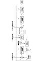
ここで、特許文献2に示されているスイッチング電源装置の構成を、図1を参照して説明する。図1に示すスイッチング電源装置は、広範囲の交流入力電圧1を直流電圧に変換する整流器2、この整流出力をDC−DCコンバータ4aに供給する昇圧型電力変換器3a、その制御を行うPFC制御回路42a、負荷の状態を検出する負荷検出回路41、出力電圧の制御を行う出力電圧制御部43、PFC制御回路の動作/停止を切り替えるPFCオン/オフ回路44を備えている。The power supply device of
Here, the configuration of the switching power supply shown in
PFCオン/オフ回路44は、負荷検出回路41の検出出力値と負荷状態を判定するための判定基準値とを比較し、その比較結果によりPFC制御回路42aはPFCコンバータの動作又は停止を行なう。
The PFC on / off
しかし、特許文献1の電源装置では、負荷に関係なく入力電圧のみによってPFCコンバータの出力電圧が決まってしまうという問題があった。特許文献2の電源装置では、負荷の軽重を検出し、フィードバックするための専用の回路が必要になる、という問題があった。
However, the power supply device of Patent Document 1 has a problem that the output voltage of the PFC converter is determined only by the input voltage regardless of the load. The power supply device of
そこで、この発明の目的は、負荷からのフィードバックを得ることなく、負荷の軽重に応じて自動的且つ連続的にPFCコンバータの出力電圧を最適な値に制御できるようにしたスイッチング電源装置を提供することにある。 SUMMARY OF THE INVENTION Accordingly, an object of the present invention is to provide a switching power supply apparatus that can automatically and continuously control the output voltage of a PFC converter to an optimum value according to the load weight without obtaining feedback from the load. There is.
前記課題を解決するために、この発明は次のように構成する。
(1)交流入力電源から入力される交流電圧を整流する整流回路と、前記整流回路の後段に接続された、インダクタ及びスイッチング素子を含む直列回路と、前記スイッチング素子に並列接続された整流平滑回路と、前記交流入力電源から入力される入力電流が前記交流電圧に対して相似形となるように前記スイッチング素子を制御するスイッチング制御手段と、を備えたPFCコンバータと、
前記PFCコンバータの後段に接続された、少なくとも1次巻線及び2次巻線を有するトランスと、前記1次巻線に接続される1次側回路と、前記2次巻線に接続されて負荷へ電源電圧を出力する2次側回路とを含む絶縁型DC−DCコンバータと、を有するスイッチング電源装置であって、
前記交流入力電源から入力される入力電圧を検出する入力電圧検出手段と、
前記インダクタに流れるまたは前記スイッチング素子に流れる電流を検出する電流検出手段と、
前記整流平滑回路の出力電圧を検出する出力電圧検出手段と、
を備え、
前記スイッチング制御手段は、前記出力電圧の目標値に対する前記出力電圧の検出値の誤差である出力電圧誤差と前記入力電圧の検出値との積を電流基準振幅値とし、この電流基準振幅値と前記電流検出手段によって検出された電流との差に応じて前記スイッチング素子のオン時間を制御する手段であり、
前記負荷が軽負荷状態から重負荷状態になるにつれて、前記出力電圧が上昇するように、前記出力電圧の目標値または前記出力電圧誤差を前記電流基準振幅値の比例値で補正する出力電圧制御値補正手段を設けたことを特徴とする。In order to solve the above problems, the present invention is configured as follows.
(1) A rectifying circuit for rectifying an AC voltage input from an AC input power supply, a series circuit including an inductor and a switching element connected to a subsequent stage of the rectifying circuit, and a rectifying / smoothing circuit connected in parallel to the switching element. And a switching control means for controlling the switching element so that an input current input from the AC input power source is similar to the AC voltage, and a PFC converter,
A transformer having at least a primary winding and a secondary winding, connected to a subsequent stage of the PFC converter, a primary circuit connected to the primary winding, and a load connected to the secondary winding A switching power supply comprising an isolated DC-DC converter including a secondary circuit that outputs a power supply voltage to
Input voltage detection means for detecting an input voltage input from the AC input power supply;
Current detection means for detecting a current flowing through the inductor or the switching element;
Output voltage detecting means for detecting the output voltage of the rectifying and smoothing circuit;
With
The switching control means uses a product of an output voltage error, which is an error of a detected value of the output voltage with respect to a target value of the output voltage, and a detected value of the input voltage as a current reference amplitude value. Means for controlling the on-time of the switching element according to the difference between the current detected by the current detection means;
An output voltage control value for correcting the output voltage target value or the output voltage error with a proportional value of the current reference amplitude value so that the output voltage increases as the load changes from a light load state to a heavy load state. A correction means is provided.
(2)交流入力電源から入力される交流電圧を整流する整流回路と、前記整流回路の後段に接続された、インダクタ及びスイッチング素子を含む直列回路と、前記スイッチング素子に並列接続された整流平滑回路と、前記交流入力電源から入力される入力電流が前記交流電圧に対して相似形となるように前記スイッチング素子を制御するスイッチング制御手段と、を備えたPFCコンバータと、
前記PFCコンバータの後段に接続された、少なくとも1次巻線及び2次巻線を有するトランスと、前記1次巻線に接続される1次側回路と、前記2次巻線に接続されて負荷へ電源電圧を出力する2次側回路とを含む絶縁型DC−DCコンバータと、を有するスイッチング電源装置であって、
前記交流入力電源から入力される入力電圧を検出する入力電圧検出手段と、
前記インダクタに流れる電流または前記スイッチング素子に流れる電流を検出する電流検出手段と、
前記整流平滑回路の出力電圧を検出する出力電圧検出手段と、
を備え、
前記スイッチング制御手段は、前記出力電圧の目標値に対する前記出力電圧の検出値の誤差である出力電圧誤差と前記入力電圧の検出値との積を電流基準振幅値とし、この電流基準振幅値と前記電流検出手段によって検出された電流との差に応じて前記スイッチング素子のオン時間を制御する手段であり、
前記負荷が軽負荷状態から重負荷状態になるにつれて、前記出力電圧が上昇するように、前記出力電圧の目標値または前記出力電圧誤差を、前記電流検出手段により検出された電流の実効値または平均値で補正する出力電圧制御値補正手段を設けたことを特徴とする。
(2) A rectifier circuit for rectifying an AC voltage input from an AC input power supply, a series circuit including an inductor and a switching element connected to a subsequent stage of the rectifier circuit, and a rectifying / smoothing circuit connected in parallel to the switching element. And a switching control means for controlling the switching element so that an input current input from the AC input power source is similar to the AC voltage, and a PFC converter,
A transformer having at least a primary winding and a secondary winding, connected to a subsequent stage of the PFC converter, a primary circuit connected to the primary winding, and a load connected to the secondary winding A switching power supply comprising an isolated DC-DC converter including a secondary circuit that outputs a power supply voltage to
Input voltage detection means for detecting an input voltage input from the AC input power supply;
Current detection means for detecting a current flowing through the inductor or a current flowing through the switching element;
Output voltage detecting means for detecting the output voltage of the rectifying and smoothing circuit;
With
The switching control means uses a product of an output voltage error, which is an error of a detected value of the output voltage with respect to a target value of the output voltage, and a detected value of the input voltage as a current reference amplitude value. Means for controlling the on-time of the switching element according to the difference between the current detected by the current detection means;
As the load is changed from a light load state to a heavy load state, the target value of the output voltage or the output voltage error is calculated as an effective value or an average of the current detected by the current detection unit so that the output voltage increases. characterized by providing an output voltage control value correcting means for correcting a value.
(3)前記スイッチング制御手段及び前記出力電圧制御値補正手段は、前記出力電圧目標値に相当するディジタル値を保持するDSP(Digital Signal Processor)で構成され、前記出力電圧制御値補正手段は、前記ディジタル値を前記電流基準振幅値の比例値で補正するようにしたことを特徴とする。 (3) The switching control means and the output voltage control value correction means are configured by a DSP (Digital Signal Processor) that holds a digital value corresponding to the output voltage target value, and the output voltage control value correction means The digital value is corrected by a proportional value of the current reference amplitude value.
この発明によれば、負荷の軽重に応じて、PFCコンバータの出力電圧値がそれぞれ最適な値に設定され、後段のDC−DCコンバータの電力変換効率を負荷状態に応じて最適化でき、その結果、AC−DCコンバータ全体としての電力変換効率を高めることができる。 According to the present invention, the output voltage value of the PFC converter is set to an optimum value according to the weight of the load, and the power conversion efficiency of the subsequent DC-DC converter can be optimized according to the load state. The power conversion efficiency of the entire AC-DC converter can be increased.
《第1の実施形態》
第1の実施形態に係るスイッチング電源装置201について図2〜図7を参照して説明する。
図2は第1の実施形態に係るスイッチング電源装置201の回路図である。図2において符号P11,P12はPFCコンバータ101の入力端、符号P21,P22はPFCコンバータ101の出力端である。入力端P11−P12には商用交流電源である交流入力電源Vacが入力され、出力端P21−P22にはDC−DCコンバータ100が接続される。<< First Embodiment >>
A switching
FIG. 2 is a circuit diagram of the switching
DC−DCコンバータ100は、少なくとも1次巻線及び2次巻線を有するトランスと、その1次巻線に接続される1次側回路と、2次巻線に接続されて負荷へ電源電圧を出力する2次側回路とを含む絶縁型DC−DCコンバータである。
DC−DCコンバータ100の出力には負荷99が接続され、DC−DCコンバータ100によって安定化された直流電圧が供給される。The DC-
A
PFCコンバータ101の入力段には交流入力電源Vacの交流電圧を全波整流するダイオードブリッジB1を設けている。ダイオードブリッジB1はこの発明の「整流回路」に相当する。ダイオードブリッジB1の出力側にはインダクタL1及びスイッチング素子Q1、さらに電流検出用抵抗Rcdの直列回路を接続している。スイッチング素子Q1の両端には、ダイオードD1及び平滑コンデンサC1で構成される整流平滑回路を並列接続している。前記インダクタL1、スイッチング素子Q1、ダイオードD1及び平滑コンデンサC1によっていわゆる昇圧チョッパ回路を構成している。
The input stage of the
電流検出用抵抗Rcd及びその信号を入力するディジタル信号処理回路13の入力部は、この発明の「電流検出手段」に相当する。
The current detection resistor Rcd and the input portion of the digital
ダイオードブリッジB1の出力側の両端間には入力電圧検出回路11を設けている。また出力端P21−P22間に出力電圧検出回路12を設けている。ディジタル信号処理回路13はDSPで構成していて、ディジタル信号処理によってこのPFCコンバータ101を制御する。すなわち、ディジタル信号処理回路13は入力電圧検出回路11の出力信号をディジタル値で入力し、交流入力電源の電圧の瞬時値を検知する。また、前記出力電圧の目標値に相当するディジタル値を保持し、出力電圧検出回路12の出力信号を入力して出力電圧を検知するとともにスイッチング素子Q1を所定のスイッチング周波数でオン/オフする。
An input voltage detection circuit 11 is provided between both ends on the output side of the diode bridge B1. An output
ディジタル信号処理回路13は、この発明の「スイッチング制御手段」に相当する。前記入力電圧検出回路11及びその信号を入力するディジタル信号処理回路13の入力部は、この発明の「入力電圧検出手段」に相当する。また、前記出力電圧検出回路12及びその信号を入力するディジタル信号処理回路13の入力部は、この発明の「出力電圧検出手段」に相当する。
The digital
さらに、ディジタル信号処理回路13はDC−DCコンバータ100との間で通信を行うためのポートを備えていて、たとえばデータの通信または信号の入出力を行い、DC−DCコンバータ100に対してコンバータの状態等を常に送信したり、入力電圧、出力電圧、出力電流等を送信したり、DC−DCコンバータ100側から負荷状態等を受信してスイッチング制御に反映したりする。
Further, the digital
図3は、電流連続モードで制御が行われている状態におけるスイッチング周期の単位でのPFCコンバータ101の電圧・電流の波形図である。
FIG. 3 is a waveform diagram of the voltage / current of the
ディジタル信号処理回路13は、PFCコンバータ101に対する入力電流、すなわちインダクタL1に流れる電流の平均値、が全波整流波形に相似形となるようにスイッチング制御を行う。このようにして入力電圧と相似形の入力電流が流れることにより、高調波が抑制され、力率が改善される。
The digital
図3において(A)は商用電源周波数の半周期単位での、インダクタL1に流れる電流の平均値Iiの電流波形、(B)はその一部の時間軸を拡大して表した、スイッチング周期の単位でのインダクタL1に流れる電流ILの波形図、(C)はスイッチング素子Q1のドレイン−ソース間電圧Vdsの波形図である。 In FIG. 3, (A) is a current waveform of the average value Ii of the current flowing through the inductor L1 in a unit of a half cycle of the commercial power supply frequency, and (B) is an enlarged part of the time axis of the switching cycle. A waveform diagram of the current IL flowing through the inductor L1 in units, (C) is a waveform diagram of the drain-source voltage Vds of the switching element Q1.
スイッチング素子Q1のオン期間TonではインダクタL1に電流ILが流れ、インダクタL1の両端間電圧及びインダクタL1のインダクタンスに応じて定まる傾きで電流ILは上昇する。その後、スイッチング素子Q1のオフ期間Toffで、インダクタL1の両端電圧とそのインダクタンスによって定まる傾きで電流ILは下降する。このように電流リップルΔILの幅でインダクタL1に流れる電流ILがスイッチング周期で変動する。 In the ON period Ton of the switching element Q1, the current IL flows through the inductor L1, and the current IL increases with a slope determined according to the voltage across the inductor L1 and the inductance of the inductor L1. Thereafter, the current IL decreases with an inclination determined by the voltage across the inductor L1 and its inductance during the OFF period Toff of the switching element Q1. As described above, the current IL flowing through the inductor L1 with the width of the current ripple ΔIL varies in the switching cycle.
図4は、DC−DCコンバータ100への供給電力PoとPFCコンバータ101の出力電圧Voとの関係を示す図である。
例えば、DC−DCコンバータ100への供給電力Po=0のとき、PFCコンバータの出力電圧Voは290V、DC−DCコンバータ100への供給電力Po=1600Wのとき、PFCコンバータの出力電圧Voは約390Vとする。FIG. 4 is a diagram showing the relationship between the power supply Po to the DC-
For example, when the power supply Po to the DC-
PFCコンバータの出力電圧の最小値は次の条件を満足するように決定する。
(1)全入力電圧で昇圧動作させるために、交流入力電源から入力される電圧のピーク値より高くする。
(2)E=CV2/2 のエネルギーを瞬時停電で所定時間以上供給する。
(3)後段のDC−DCコンバータが動作可能な最低電圧以上の電圧を出力する。The minimum value of the output voltage of the PFC converter is determined so as to satisfy the following condition.
(1) In order to perform a boost operation with all input voltages, the peak value of the voltage input from the AC input power source is set higher.
(2) for supplying a predetermined time or more the energy of E = CV 2/2 with instantaneous power failure.
(3) A voltage equal to or higher than the lowest voltage at which the subsequent DC-DC converter can operate is output.
上記(2)を考慮すると、負荷が軽いときは出力電圧を低く、負荷が重いときには出力電圧を高くする必要がある。出力電圧を負荷に応じて変更することで、軽〜中負荷の領域で不必要な昇圧を行わなくてすむため、効率を改善することができる。 Considering the above (2), it is necessary to lower the output voltage when the load is light and to increase the output voltage when the load is heavy. By changing the output voltage according to the load, unnecessary boosting is not required in the light to medium load region, so that the efficiency can be improved.
設計例は次のとおりである。
コンデンサC1の容量:980μF
DC−DCコンバータ100の最低動作電圧:290V
瞬時停電保持時間:25ms
図5は、図2に示したディジタル信号処理回路13の処理内容をブロック化して表した図である。
図5において、加算要素31は、後述する出力電圧目標値Vrefに対する出力電圧検出値voの誤差evを求める。出力電圧誤差増幅器32は、誤差evに対して所定の比例係数を乗じて電流基準振幅値Vmを求める(通常、PFCにおける誤差増幅器は、出力電圧が入力電圧のリップルに応答しないようにする必要があるため、高域遮断特性を持つ)。乗算器33は、電流基準振幅値Vmに対して入力電圧検出値Viを乗じて電流基準値irを求める。加算要素34は、電流基準値irに対するインダクタ電流検出値iLの差分である入力電流誤差値eiを求める。入力電流誤差増幅器35は入力電流誤差値eiに応じてパルス生成器に対する変調信号Dを発生する。パルス生成器36は前記変調信号Dに基づいて、二値論理信号であるパルス信号を出力する。このパルス信号はスイッチング素子Q1に対するスイッチング制御信号である。すなわちスイッチング制御信号を前記電流誤差値eiに応じた値でPWM変調する。これによりスイッチング素子Q1のオン時間が制御される。A design example is as follows.
Capacitor C1 capacitance: 980 μF
Minimum operating voltage of DC-DC converter 100: 290V
Instantaneous power outage retention time: 25 ms
FIG. 5 is a block diagram showing the processing contents of the digital
In FIG. 5, the
係数要素38は前記電流基準振幅値Vmに対して所定の係数を乗じた値、すなわち前記電流基準振幅値Vmの比例値を発生する。加算要素39は、係数要素38が発生する値を基準値vr0に加算して出力電圧目標値Vrefを求める。この係数要素38及び加算要素39が、この発明の「出力電圧制御値補正手段」に相当する。
The
係数要素38は、出力電圧誤差増幅器32の出力Vmに応じて出力電圧目標値Vrefを変化させる。そのため、条件によっては異常発振することがある。そのような場合は係数要素38に高域遮断特性をもたせる。このことにより、電流基準振幅値Vmが急激に変化する場合でもVrefの変化は低速になって、過渡的な応答が回避できる。
The
なお、以上に示した例では、出力電圧の目標値Vrefを電流基準振幅値の比例値で補正する例を示したが、補正対象は出力電圧誤差evであってもよい。 In the example described above, the target value Vref of the output voltage is corrected with the proportional value of the current reference amplitude value. However, the correction target may be the output voltage error ev.
図6は、出力電圧のフィードバック制御に関するブロック図である。図6(A)は、図5に示した、加算要素31、出力電圧誤差増幅器32、係数要素38、加算要素39によるフィードバック系のブロック図である。図6(B)は、比較例であり、図5に示した係数要素38及び加算要素39を設けない場合のブロック図である。
FIG. 6 is a block diagram relating to feedback control of the output voltage. FIG. 6A is a block diagram of a feedback system including the
図6(B)に示す比較例のフィードバック系では、出力電圧目標値Vrefに対する出力電圧検出値voの誤差evが求められ、出力電圧誤差増幅器32は電流基準振幅値Vmを出力し、制御対象(PFCコンバータ)50は電流基準振幅値Vmを基にして出力電圧(出力電圧検出値vo)を制御する。
In the feedback system of the comparative example shown in FIG. 6B, the error ev of the output voltage detection value vo with respect to the output voltage target value Vref is obtained, and the output
一方、図6(A)に示すフィードバック系では、更に係数要素38が電流基準振幅値Vmに対して係数を乗じた値を基準値vr0に加算して出力電圧目標値Vrefを補正する。
On the other hand, in the feedback system shown in FIG. 6A, the
図7は図6(A),(B)に示したフィードバック系の負荷供給電力対出力電圧の関係を示す図である。
図6(B)に示した通常のP制御(P補償)では、負荷が重くなることにともなって出力電圧が低下するが、図6(A)の「P補償+目標値補正」の制御で出力電圧が一定とすることができる。しかし、本発明はさらに、その目標値の補正量を大きくして、負荷が重くなる程(軽負荷状態から重負荷状態になるにつれて)、出力電圧を上昇させる。FIG. 7 is a diagram showing the relationship between the load supply power and the output voltage of the feedback system shown in FIGS. 6 (A) and 6 (B).
In the normal P control (P compensation) shown in FIG. 6B, the output voltage decreases as the load becomes heavier. However, the control of “P compensation + target value correction” in FIG. The output voltage can be constant. However, the present invention further increases the correction amount of the target value, and increases the output voltage as the load becomes heavier (as the light load state changes to the heavy load state).
前記出力電圧誤差増幅器32の出力Vmは電流基準振幅の情報であるため、負荷が増大するとVmも増大する。よってVmに応じてVrefを補正することで、出力電圧を増加させることができる。
このようにして、負荷が変動してもそれぞれに適した出力電圧に変更され、効率を改善することができる。Since the output Vm of the output
In this way, even if the load fluctuates, it is changed to an output voltage suitable for each, and the efficiency can be improved.
以上に示したように、ディジタル信号処理回路13をDSPで構成することにより、信号の劣化やノイズの混入、素子バラツキの影響がないため、高精度な目標値の補正が行える。また、条件判断や条件分岐を細かく複雑に行える。例えば負荷が重いときは目標値も大きくなっているが、この状態で負荷が急激に小さくなったことを検出すると、出力電圧目標値Vrefを初期値にリセットする。このことによって、負荷が急激に小さくなったときの出力電圧の跳ね上がりを抑制する。
As described above, by configuring the digital
《第2の実施形態》
図8は、第2の実施形態に係るスイッチング電源装置に適用するディジタル信号処理回路(DSP)の処理内容をブロック化して表した図である。スイッチング電源装置全体の構成は図2に示したものと同様である。
図8おいて、加算要素31は、出力電圧目標値Vrefに対する出力電圧検出値voの誤差evを求める。出力電圧誤差増幅器32は、誤差evに対して所定の比例係数を乗じて電流基準振幅値Vmを求める。乗算器33は、電流基準振幅値Vmに対して入力電圧検出値Viを乗じて電流基準値irを求める。加算要素34は、電流基準値irに対するインダクタ電流検出値iLの差分である入力電流誤差値eiを求める。入力電流誤差増幅器35は入力電流誤差値eiに応じてパルス生成器に対する変調信号Dを発生する。パルス生成器36は前記変調信号Dに基づいてパルス信号を出力する。<< Second Embodiment >>
FIG. 8 is a block diagram showing the processing contents of the digital signal processing circuit (DSP) applied to the switching power supply device according to the second embodiment. The overall configuration of the switching power supply is the same as that shown in FIG.
In FIG. 8, the adding
実効値検出部37はインダクタ電流検出値iLの実効値または平均値に対して所定の係数を乗じた値を発生する。加算要素39は、実効値検出部37が発生する値を基準値vr0に加算して出力電圧目標値Vrefを求める。この実効値検出部37及び加算要素39が、この発明の「出力電圧制御値補正手段」に相当する。
The effective
このように負荷供給電流の実効値または平均値によって負荷供給電力を検出し、負荷が増大すると、それに応じてvrefを補正することで、出力電圧を増加させることができる。
このようにして、負荷が変動してもそれぞれに適した出力電圧に変更され、効率を改善することができる。As described above, when the load supply power is detected based on the effective value or average value of the load supply current and the load increases, the output voltage can be increased by correcting vref accordingly.
In this way, even if the load fluctuates, it is changed to an output voltage suitable for each, and the efficiency can be improved.
なお、第1の実施形態の場合と同様に、出力電圧の目標値Vrefを電流基準振幅値の比例値で補正することに代えて、出力電圧誤差evを電流基準振幅値の比例値で補正するようにしてもよい。 As in the first embodiment, the output voltage error ev is corrected with the proportional value of the current reference amplitude value instead of correcting the target value Vref of the output voltage with the proportional value of the current reference amplitude value. You may do it.
《第3の実施形態》
第3の実施形態に係るスイッチング電源装置は、第1・第2の実施形態で示したスイッチング電源装置において、入力電圧も考慮し、入力電圧に応じてPFCコンバータの出力電圧を変化させるものである。図9は、入力電圧をパラメータとした、出力電力Poに対する出力電圧Voの特性を示す図である。<< Third Embodiment >>
The switching power supply according to the third embodiment changes the output voltage of the PFC converter according to the input voltage in consideration of the input voltage in the switching power supply shown in the first and second embodiments. . FIG. 9 is a diagram illustrating the characteristics of the output voltage Vo with respect to the output power Po, using the input voltage as a parameter.
既に述べたとおり、PFCコンバータの出力電圧は入力電圧より高くする必要がある。したがって、その条件を満足させるために、入力電圧を考慮してPFCコンバータの出力電圧を変更するには、例えば次の方法で変更する。 As already described, the output voltage of the PFC converter needs to be higher than the input voltage. Therefore, in order to satisfy the condition, the output voltage of the PFC converter is changed in consideration of the input voltage, for example, by the following method.
図9(A)に示すように、出力電力Poに対する出力電圧Voの傾き・切片を入力電圧に応じて変更する。
または、図9(B)に示すように、出力電圧の下限を設定する。すなわち、負荷の変動に対して出力電圧が一定となる領域と変動する領域を設ける。As shown in FIG. 9A, the slope / intercept of the output voltage Vo with respect to the output power Po is changed according to the input voltage.
Alternatively, as shown in FIG. 9B, the lower limit of the output voltage is set. That is, a region where the output voltage is constant and a region where the output voltage fluctuates with respect to the load variation are provided.
このようにして、PFCコンバータの出力電圧を入力電圧より高く保ちつつ、DC−DCコンバータの電力変換効率を負荷状態に応じて最適にでき、その結果、AC−DCコンバータ全体としての電力変換効率を高めることができる。 In this way, while maintaining the output voltage of the PFC converter higher than the input voltage, the power conversion efficiency of the DC-DC converter can be optimized according to the load state. As a result, the power conversion efficiency of the entire AC-DC converter can be improved. Can be increased.
《第4の実施形態》
第1の実施形態で図2に示したスイッチング電源装置では、DSPによるディジタル信号処理回路13を用いてスイッチング制御を行うようにしたが、第4の実施形態は、図5に示した出力電圧誤差増幅器32をアナログ素子で構成する例である。<< Fourth Embodiment >>
In the switching power supply apparatus shown in FIG. 2 in the first embodiment, the switching control is performed using the digital
図10は第4の実施形態に係る出力電圧誤差増幅器の回路図である。オペアンプOPの非反転入力端子(+)の入力電圧Vrefは次の(1)式で表される。ここでVmはオペアンプOPの出力電圧(出力電圧誤差増幅器の出力)、Voは出力電圧検出値、Vrefは出力電圧目標値である。 FIG. 10 is a circuit diagram of an output voltage error amplifier according to the fourth embodiment. The input voltage Vref at the non-inverting input terminal (+) of the operational amplifier OP is expressed by the following equation (1). Here, Vm is an output voltage of the operational amplifier OP (output of the output voltage error amplifier), Vo is an output voltage detection value, and Vref is an output voltage target value.
Vref=(vr0/Rr1+Vm/Rr3)/(1/Rr1+1/Rr2+1/Rr3) …(1)
但し、抵抗Rr2に対してコンデンサCrefが並列接続されているので、このコンデンサCrefの容量が大きくなるほど、時間経過あたりの出力電圧目標値Vrefの変化は小さくなる。すなわちローパスフィルタの作用を備えることになる。Vref = (vr0 / Rr1 + Vm / Rr3) / (1 / Rr1 + 1 / Rr2 + 1 / Rr3) (1)
However, since the capacitor Cref is connected in parallel to the resistor Rr2, the change in the output voltage target value Vref with the lapse of time decreases as the capacitance of the capacitor Cref increases. That is, it has a function of a low-pass filter.
《第5の実施形態》
図11は第5の実施形態に係るスイッチング電源装置202の回路図である。また図12はPFCコンバータ104の4つのタイミングでの電流経路を示す図である。<< Fifth Embodiment >>
FIG. 11 is a circuit diagram of the switching
図11に示すPFCコンバータ104はダイオードブリッジを介さずに2つのインダクタと2つのスイッチング素子とを備えた、ダイオードブリッジレスPFCコンバータである。
A
図11において、符号P11,P12はPFCコンバータ104の入力端、符号P21,P22はPFCコンバータ104の出力端である。入力端P11−P12には商用交流電源である交流入力電源Vacが入力され、出力端P21−P22にはDC−DCコンバータ100が接続される。
In FIG. 11, reference signs P <b> 11 and P <b> 12 are input ends of the
DC−DCコンバータ100の出力には負荷99が接続され、DC−DCコンバータ100によって安定化された直流電圧が供給される。
A
PFCコンバータ104の入力段には、入力電圧検出回路11を設け、一方のラインにインダクタL1を直列に接続している。インダクタL1の後段には、ダイオードD1,D2及びスイッチング素子Q1,Q2によるブリッジ回路を接続している。スイッチング素子Q1,Q2のソースとグランドとの間には電流検出用抵抗R21,R22を接続している。ブリッジ回路の出力には平滑コンデンサC1からなる平滑回路を並列接続している。
An input voltage detection circuit 11 is provided at the input stage of the
図12(A)は、交流入力電源の正の半サイクルで、スイッチング素子Q1,Q2が共にオン状態であるときの電流経路、図12(B)は、交流入力電源の正の半サイクルで、スイッチング素子Q1,Q2が共にオフ状態であるときの電流経路である。 12A is a positive half cycle of the AC input power supply, and the current path when the switching elements Q1 and Q2 are both on. FIG. 12B is a positive half cycle of the AC input power supply. This is a current path when the switching elements Q1, Q2 are both in the off state.
また、図12(C)は、交流入力電源の負の半サイクルで、スイッチング素子Q1,Q2が共にオン状態であるときの電流経路、図12(D)は、交流入力電源の負の半サイクルで、スイッチング素子Q1,Q2が共にオフ状態であるときの電流経路である。 12C shows the negative half cycle of the AC input power supply, and the current path when both the switching elements Q1 and Q2 are on. FIG. 12D shows the negative half cycle of the AC input power supply. Thus, this is a current path when both of the switching elements Q1, Q2 are in the OFF state.
交流入力電源の正の半サイクルで、Q1,Q2がオン状態であるとき、図12(A)に示す経路で電流が流れて、インダクタL1に励磁エネルギーが蓄積され、Q1,Q2がオフ状態であるとき、図12(B)に示す経路で電流が流れて、インダクタL1から励磁エネルギーが放出される。このとき、Q2の寄生ダイオードを介して電流が流れる。同様に、交流入力電源の負の半サイクルで、Q1,Q2がオン状態であるとき、図12(C)に示す経路で電流が流れて、インダクタL1に励磁エネルギーが蓄積され、Q1,Q2がオフ状態であるとき、図12(D)に示すタイミングで、インダクタL1から励磁エネルギーが放出される。このとき、Q1の寄生ダイオードを介して電流が流れる。 When Q1 and Q2 are in the ON state in the positive half cycle of the AC input power supply, current flows through the path shown in FIG. 12A, and the excitation energy is accumulated in the inductor L1, and Q1 and Q2 are in the OFF state. At a certain time, a current flows through the path shown in FIG. 12B, and excitation energy is released from the inductor L1. At this time, a current flows through the parasitic diode of Q2. Similarly, when Q1 and Q2 are on in the negative half cycle of the AC input power supply, current flows through the path shown in FIG. 12C, and the excitation energy is accumulated in the inductor L1, and Q1 and Q2 are When in the off state, excitation energy is released from the inductor L1 at the timing shown in FIG. At this time, a current flows through the parasitic diode of Q1.
電流検出用抵抗R21は、交流入力電源の正の半サイクルでQ1のオン期間において、インダクタL1に流れる電流を検出するために設けている。また、電流検出用抵抗R22は、交流入力電源の負の半サイクルでQ2のオン期間において、インダクタL1に流れる電流を検出するために設けている。図11に示したディジタル信号処理回路13は、スイッチング素子Q1,Q2のオン期間の中央で、電流検出用抵抗R21,R22の降下電圧をサンプリングすることによってインダクタL1に流れる電流の平均値を検出する。
The current detection resistor R21 is provided to detect the current flowing through the inductor L1 during the ON period of Q1 in the positive half cycle of the AC input power supply. The current detection resistor R22 is provided to detect the current flowing through the inductor L1 during the ON period of Q2 in the negative half cycle of the AC input power supply. The digital
図11に示したディジタル信号処理回路13は、電流連続モードで平均電流制御を行う場合、出力電圧の目標値に対する出力電圧の検出値の誤差である出力電圧誤差と入力電圧の検出値との積を電流基準振幅値とし、この電流基準振幅値と、スイッチング素子Q1,Q2に流れる電流との差に応じてスイッチング素子Q1,Q2のオン時間を制御する。そして、負荷が軽負荷状態から重負荷状態になるにつれて、出力電圧が上昇するように、出力電圧の目標値または出力電圧誤差を電流基準振幅値の比例値で補正する。
When the average current control is performed in the continuous current mode, the digital
また、図11に示したディジタル信号処理回路13は、臨界モードでピーク電流制御を行う場合、出力電圧の目標値に対する出力電圧の検出値の誤差である出力電圧誤差と入力電圧の検出値との積を電流基準振幅値とし、スイッチング素子Q1またはQ2に流れる電流が電流基準振幅値に達したときにスイッチング素子Q1またはQ2をオフする。そして、負荷が軽負荷状態から重負荷状態になるにつれて、出力電圧が上昇するように、出力電圧の目標値または出力電圧誤差を電流基準振幅値の比例値で補正する。
When the digital
《第6の実施形態》
図13は第6の実施形態に係るスイッチング電源装置203の回路図である。また図14は図13各部の電圧・電流波形図である。<< Sixth Embodiment >>
FIG. 13 is a circuit diagram of the switching
図2や図11に示した例ではDC−DCコンバータ100への出力電圧Voを出力電圧検出回路12で検出するようにしたが、PFCコンバータの出力にDC−DCコンバータ等の電圧コンバータが接続される場合には、そのDC−DCコンバータの出力電圧を検出してPFCコンバータの制御に用いることができる。第6の実施形態はその例である。図13においてPFCコンバータは、ダイオードブリッジB1、インダクタL1、ダイオードD1、スイッチング素子Q1、平滑コンデンサC1を備えている。この構成は第1の実施形態で図2に示したものと同様である。但し、図2に示した電流検出用抵抗Rcd及び入力電圧検出回路11の構成については簡略化して表している。
In the example shown in FIGS. 2 and 11, the output voltage Vo to the DC-
スイッチング電源装置203は、トランスT2、スイッチング素子Q2、整流ダイオードD2及び平滑コンデンサC2を含むDC−DCコンバータを備えている。
The switching
図13においてディジタル信号処理回路13はDSPで構成されるが、この例では動作内容を等価的な回路で表している。すなわち、PFC制御部は、第1の実施形態で図5に示した構成と同様である。但し、出力電圧誤差増幅器32の出力値である電流基準振幅値Vmを入力し、スイッチング素子Q1に対するPWM信号(PWM1)を出力する回路部分は単一のブロック30で簡略化して表している。
In FIG. 13, the digital
前記ディジタル信号処理回路13においてDC−DCコンバータ制御部は、前記DC−DCコンバータの出力電圧Vo2の変化に応じて変化する検出電圧Virを発生する出力電圧検出回路を備えている。また前記検出電圧Virと、スイッチング素子Q2に流れる電流iFETの比例電圧とを比較するコンパレータ60、コンパレータ60の出力でリセットされ、発振器62の出力でセットされるフリップフロップ61を備えている。
In the digital
図14に示すように、発振器62の出力がハイレベルになった時、PWM2が立ち上がり、前記DC−DCコンバータのスイッチング素子Q2に流れる電流iFETの電流値が前記出力電圧検出値Virを超えた時、フリップフロップ61の出力信号PWM2が立ち下がる。
As shown in FIG. 14, when the output of the oscillator 62 becomes high level, PWM2 rises, and when the current value of the current iFET flowing through the switching element Q2 of the DC-DC converter exceeds the output voltage detection value Vir. The output signal PWM2 of the flip-
DC−DCコンバータの出力電力が大きくなると出力電圧検出値Virは高くなる関係にある。 The output voltage detection value Vir increases as the output power of the DC-DC converter increases.
前記PFC制御部において係数要素38は前記出力電圧検出値Virに対して所定の係数を乗じた値を発生する。加算要素39は、係数要素38が発生する値を基準値Vr0に加算して出力電圧目標値Vrefを求める。以降の動作は図5及び図8に示した回路の動作と同様である。
In the PFC controller, the
このようにしてPFCコンバータの出力電圧を入力して動作するDC−DCコンバータの出力電圧検出値を基にしてPFCコンバータの出力電圧を変更するようにしてもよい。 In this way, the output voltage of the PFC converter may be changed based on the detected output voltage of the DC-DC converter that operates by inputting the output voltage of the PFC converter.
B1…ダイオードブリッジ
C1…平滑コンデンサ
D…変調信号
D1,D2…ダイオード
ei…入力電流誤差値
ev…出力電圧誤差
Ii…平均値
iL…インダクタ電流検出値
ir…電流基準値
L1…インダクタ
P11,P12…入力端
P21,P22…出力端
Q1,Q2…スイッチング素子
R21,R22…電流検出用抵抗
Rcd…電流検出用抵抗
Vac…交流入力電源
Vds…ソース間電圧
Vi…入力電圧検出値
Vm…電流基準振幅値
Vo…出力電圧
vo…出力電圧検出値
vr0…基準値
Vref…出力電圧目標値
11…入力電圧検出回路
12…出力電圧検出回路
13…ディジタル信号処理回路
31…加算要素
32…出力電圧誤差増幅器
33…乗算器
34…加算要素
35…入力電流誤差増幅器
36…パルス生成器
37…実効値検出部
38…係数要素
39…加算要素
99…負荷
100…DC−DCコンバータ
101…PFCコンバータ
104…PFCコンバータ
201〜203…スイッチング電源装置B1 ... Diode bridge C1 ... Smoothing capacitor D ... Modulation signal D1, D2 ... Diode ei ... Input current error value ev ... Output voltage error Ii ... Average value iL ... Inductor current detection value ir ... Current reference value L1 ... Inductors P11, P12 ... Input terminal P21, P22 ... Output terminal Q1, Q2 ... Switching element R21, R22 ... Current detection resistor Rcd ... Current detection resistor Vac ... AC input power supply Vds ... Source voltage Vi ... Input voltage detection value Vm ... Current reference amplitude value Vo ... output voltage vo ... output voltage detection value vr0 ... reference value Vref ... output voltage target value 11 ... input
Claims (3)
前記PFCコンバータの後段に接続された、少なくとも1次巻線及び2次巻線を有するトランスと、前記1次巻線に接続される1次側回路と、前記2次巻線に接続されて負荷へ電源電圧を出力する2次側回路とを含む絶縁型DC−DCコンバータと、を有するスイッチング電源装置であって、
前記交流入力電源から入力される入力電圧を検出する入力電圧検出手段と、
前記インダクタに流れる電流または前記スイッチング素子に流れる電流を検出する電流検出手段と、
前記整流平滑回路の出力電圧を検出する出力電圧検出手段と、
を備え、
前記スイッチング制御手段は、前記出力電圧の目標値に対する前記出力電圧の検出値の誤差である出力電圧誤差と前記入力電圧の検出値との積を電流基準振幅値とし、この電流基準振幅値と前記電流検出手段によって検出された電流との差に応じて前記スイッチング素子のオン時間を制御する手段であり、
前記負荷が軽負荷状態から重負荷状態になるにつれて、前記出力電圧が上昇するように、前記出力電圧の目標値または前記出力電圧誤差を、前記電流基準振幅値の比例値で補正する出力電圧制御値補正手段を設けたスイッチング電源装置。A rectifying circuit for rectifying an AC voltage input from an AC input power supply; a series circuit including an inductor and a switching element connected to a subsequent stage of the rectifying circuit; a rectifying and smoothing circuit connected in parallel to the switching element; A switching control means for controlling the switching element so that an input current input from an AC input power supply is similar to the AC voltage, and a PFC converter comprising:
A transformer having at least a primary winding and a secondary winding, connected to a subsequent stage of the PFC converter, a primary circuit connected to the primary winding, and a load connected to the secondary winding A switching power supply comprising an isolated DC-DC converter including a secondary circuit that outputs a power supply voltage to
Input voltage detection means for detecting an input voltage input from the AC input power supply;
Current detection means for detecting a current flowing through the inductor or a current flowing through the switching element;
Output voltage detecting means for detecting the output voltage of the rectifying and smoothing circuit;
With
The switching control means uses a product of an output voltage error, which is an error of a detected value of the output voltage with respect to a target value of the output voltage, and a detected value of the input voltage as a current reference amplitude value. Means for controlling the on-time of the switching element according to the difference between the current detected by the current detection means;
Output voltage control for correcting a target value of the output voltage or the output voltage error with a proportional value of the current reference amplitude value so that the output voltage increases as the load changes from a light load state to a heavy load state. A switching power supply device provided with value correction means.
を備えたPFCコンバータと、
前記PFCコンバータの後段に接続された、少なくとも1次巻線及び2次巻線を有するトランスと、前記1次巻線に接続される1次側回路と、前記2次巻線に接続されて負荷へ電源電圧を出力する2次側回路とを含む絶縁型DC−DCコンバータと、を有するスイッチング電源装置であって、
前記交流入力電源から入力される入力電圧を検出する入力電圧検出手段と、
前記インダクタに流れる電流または前記スイッチング素子に流れる電流を検出する電流検出手段と、
前記整流平滑回路の出力電圧を検出する出力電圧検出手段と、
を備え、
前記スイッチング制御手段は、前記出力電圧の目標値に対する前記出力電圧の検出値の誤差である出力電圧誤差と前記入力電圧の検出値との積を電流基準振幅値とし、この電流基準振幅値と前記電流検出手段によって検出された電流との差に応じて前記スイッチング素子のオン時間を制御する手段であり、
前記負荷が軽負荷状態から重負荷状態になるにつれて、前記出力電圧が上昇するように、前記出力電圧の目標値または前記出力電圧誤差を、前記電流検出手段により検出された電流の実効値または平均値で補正する出力電圧制御値補正手段を設けたスイッチング電源装置。A rectifying circuit for rectifying an AC voltage input from an AC input power supply; a series circuit including an inductor and a switching element connected to a subsequent stage of the rectifying circuit; a rectifying and smoothing circuit connected in parallel to the switching element; Switching control means for controlling the switching element so that an input current input from an AC input power supply is similar to the AC voltage;
A PFC converter with
A transformer having at least a primary winding and a secondary winding, connected to a subsequent stage of the PFC converter, a primary circuit connected to the primary winding, and a load connected to the secondary winding A switching power supply comprising an isolated DC-DC converter including a secondary circuit that outputs a power supply voltage to
Input voltage detection means for detecting an input voltage input from the AC input power supply;
Current detection means for detecting a current flowing through the inductor or a current flowing through the switching element;
Output voltage detecting means for detecting the output voltage of the rectifying and smoothing circuit;
With
The switching control means uses a product of an output voltage error, which is an error of a detected value of the output voltage with respect to a target value of the output voltage, and a detected value of the input voltage as a current reference amplitude value. Means for controlling the on-time of the switching element according to the difference between the current detected by the current detection means;
As the load is changed from a light load state to a heavy load state, the target value of the output voltage or the output voltage error is calculated as an effective value or an average of the current detected by the current detection unit so that the output voltage increases. switching power supply device provided with the output voltage control value correcting means for correcting a value.
Priority Applications (1)
| Application Number | Priority Date | Filing Date | Title |
|---|---|---|---|
| JP2010517627A JP5104947B2 (en) | 2009-03-24 | 2009-09-11 | Switching power supply |
Applications Claiming Priority (4)
| Application Number | Priority Date | Filing Date | Title |
|---|---|---|---|
| JP2009071161 | 2009-03-24 | ||
| JP2009071161 | 2009-03-24 | ||
| JP2010517627A JP5104947B2 (en) | 2009-03-24 | 2009-09-11 | Switching power supply |
| PCT/JP2009/065910 WO2010109694A1 (en) | 2009-03-24 | 2009-09-11 | Switching power supply device |
Publications (2)
| Publication Number | Publication Date |
|---|---|
| JPWO2010109694A1 JPWO2010109694A1 (en) | 2012-09-27 |
| JP5104947B2 true JP5104947B2 (en) | 2012-12-19 |
Family
ID=42780399
Family Applications (1)
| Application Number | Title | Priority Date | Filing Date |
|---|---|---|---|
| JP2010517627A Expired - Fee Related JP5104947B2 (en) | 2009-03-24 | 2009-09-11 | Switching power supply |
Country Status (5)
| Country | Link |
|---|---|
| US (1) | US8630105B2 (en) |
| JP (1) | JP5104947B2 (en) |
| CN (1) | CN102308462B (en) |
| DE (1) | DE112009004573T5 (en) |
| WO (1) | WO2010109694A1 (en) |
Cited By (1)
| Publication number | Priority date | Publication date | Assignee | Title |
|---|---|---|---|---|
| WO2014158162A1 (en) * | 2013-03-28 | 2014-10-02 | Hewlett-Packard Development Company, L.P. | Converters to provide light load output |
Families Citing this family (51)
| Publication number | Priority date | Publication date | Assignee | Title |
|---|---|---|---|---|
| GB201100219D0 (en) * | 2011-01-07 | 2011-02-23 | Tdk Lambada Uk Ltd | Power factor correction device |
| JP5692721B2 (en) * | 2011-02-22 | 2015-04-01 | ニチコン株式会社 | Switching power supply |
| JP2012217309A (en) * | 2011-04-01 | 2012-11-08 | Konica Minolta Business Technologies Inc | Power-supply device and image formation apparatus |
| JP5700373B2 (en) * | 2011-04-20 | 2015-04-15 | ニチコン株式会社 | Switching power supply |
| JP5757785B2 (en) | 2011-05-19 | 2015-07-29 | ローム株式会社 | Power supply device and electronic device using the same |
| JP2012249495A (en) * | 2011-05-31 | 2012-12-13 | Kyocera Document Solutions Inc | Power supply device |
| JP2013038850A (en) * | 2011-08-04 | 2013-02-21 | Shindengen Electric Mfg Co Ltd | Power supply unit |
| KR101288227B1 (en) | 2011-12-26 | 2013-07-19 | 한국과학기술원 | Power module and distributed power supplying apparatus having the same |
| CN103430438B (en) * | 2011-12-28 | 2016-09-07 | 丰田自动车株式会社 | Fuel cell system |
| AT512995A1 (en) * | 2012-05-18 | 2013-12-15 | Fronius Int Gmbh | Method for controlling a current source, as well as current source and process controller therefor |
| JP5846085B2 (en) * | 2012-09-18 | 2016-01-20 | 株式会社豊田自動織機 | Power receiving device and non-contact power transmission device |
| JP6098311B2 (en) * | 2013-04-10 | 2017-03-22 | コニカミノルタ株式会社 | Power supply device and image forming apparatus |
| JP5958431B2 (en) * | 2013-07-19 | 2016-08-02 | 株式会社村田製作所 | Switching power supply |
| KR101567648B1 (en) * | 2013-12-18 | 2015-11-10 | 현대자동차주식회사 | Method and system for controlling battery recharge |
| CN103746342B (en) * | 2014-01-10 | 2016-09-21 | 成都芯源系统有限公司 | Boost converter, controller for boost converter and short-circuit protection method |
| US9531253B2 (en) * | 2014-01-30 | 2016-12-27 | Silicon Laboratories Inc. | Soft-start for isolated power converter |
| JP6399761B2 (en) * | 2014-02-07 | 2018-10-03 | キヤノン株式会社 | Power supply device and image forming apparatus |
| JP6254868B2 (en) * | 2014-02-17 | 2017-12-27 | 新電元工業株式会社 | Power supply |
| US9575497B2 (en) * | 2014-04-03 | 2017-02-21 | Microchip Technology Inc. | Current control circuit for linear LED driver |
| CN105004910A (en) * | 2014-04-22 | 2015-10-28 | 中兴通讯股份有限公司 | Current detection method and apparatus of PFC inductor |
| JP6328506B2 (en) * | 2014-07-09 | 2018-05-23 | 株式会社デンソー | ACDC converter control device |
| JP6199253B2 (en) * | 2014-07-25 | 2017-09-20 | 新電元工業株式会社 | Power converter and control method thereof |
| CN106489232B (en) | 2014-08-05 | 2019-01-11 | 株式会社村田制作所 | Switching power unit |
| CN106664032B (en) * | 2014-08-08 | 2019-12-03 | 飞利浦照明控股有限公司 | Converter with control loop |
| JP5950970B2 (en) * | 2014-08-25 | 2016-07-13 | 三菱電機株式会社 | Power converter |
| TWI581555B (en) | 2014-09-12 | 2017-05-01 | Alpha And Omega Semiconductor (Cayman) Ltd | Fixed on-time switching converter |
| TWI574499B (en) | 2014-09-12 | 2017-03-11 | Alpha And Omega Semiconductor (Cayman) Ltd | Fixed on-time switching type switching device |
| TWI556563B (en) | 2014-09-12 | 2016-11-01 | Alpha & Omega Semiconductor Cayman Ltd | Fixed on-time switching type switching device |
| TWI565211B (en) | 2014-09-12 | 2017-01-01 | Alpha And Omega Semiconductor (Cayman) Ltd | Constant on-time switching converter |
| TWI549412B (en) * | 2014-09-12 | 2016-09-11 | Alpha & Omega Semiconductor Cayman Ltd | Fixed on-time switching type switching device |
| US9621019B2 (en) * | 2014-11-07 | 2017-04-11 | Power Intergrations, Inc. | Indirect regulation of output current in power converter |
| CN109152143B (en) * | 2015-01-16 | 2020-06-19 | 矽力杰半导体技术(杭州)有限公司 | LED driver and LED lighting device |
| CN105988496B (en) * | 2015-02-10 | 2018-11-23 | 杨宏 | Digitize current control device |
| CN106300953B (en) * | 2015-05-15 | 2019-02-22 | 三垦电气株式会社 | Power factor correcting method, circuit of power factor correction and Switching Power Supply |
| JP6227598B2 (en) | 2015-07-15 | 2017-11-08 | ファナック株式会社 | Digital control power supply with DC-DC converter in the subsequent stage |
| JP6702112B2 (en) * | 2015-09-28 | 2020-05-27 | サンケン電気株式会社 | Switching power supply device and LED lighting circuit |
| ES2868603T3 (en) * | 2016-02-02 | 2021-10-21 | Toshiba Carrier Corp | Power conversion device |
| WO2018087960A1 (en) * | 2016-11-08 | 2018-05-17 | 三菱電機株式会社 | Power factor compensation power supply device and led lighting device |
| US10135341B1 (en) * | 2017-07-17 | 2018-11-20 | Texas Instruments Incorporated | Dual ramp modulation for a switch-mode power supply |
| JP6948918B2 (en) * | 2017-11-10 | 2021-10-13 | 株式会社Soken | Power converter control device |
| TWI685183B (en) * | 2018-07-04 | 2020-02-11 | 群光電能科技股份有限公司 | Hybrid-mode boost power factor corrector |
| KR102609536B1 (en) * | 2018-07-13 | 2023-12-05 | 삼성전자주식회사 | Electronic apparatus |
| WO2020116338A1 (en) * | 2018-12-06 | 2020-06-11 | ローム株式会社 | Electric power conversion device and control device therefor |
| JP7338189B2 (en) * | 2019-03-25 | 2023-09-05 | Tdk株式会社 | power supply |
| US10958174B1 (en) * | 2019-07-08 | 2021-03-23 | Dialog Semiconductor Inc. | Light load detector circuit for inductive DC-DC converter |
| CN110868059A (en) * | 2019-11-29 | 2020-03-06 | 广东美的制冷设备有限公司 | Drive control circuit, control method, control device and air conditioning equipment |
| CN110868061A (en) * | 2019-11-29 | 2020-03-06 | 广东美的制冷设备有限公司 | Drive control circuit, method and device, air conditioning equipment and readable storage medium |
| JP7381397B2 (en) * | 2020-04-28 | 2023-11-15 | ローム株式会社 | power supply |
| US11705808B2 (en) * | 2021-05-04 | 2023-07-18 | Texas Instruments Incorporated | Charge mode control for power factor correction circuit |
| TWI788184B (en) * | 2022-01-07 | 2022-12-21 | 偉詮電子股份有限公司 | Power supply with optional pfc, and control method thereof |
| TWI818582B (en) * | 2022-06-09 | 2023-10-11 | 群光電能科技股份有限公司 | Voltage converter |
Citations (2)
| Publication number | Priority date | Publication date | Assignee | Title |
|---|---|---|---|---|
| JP2004194425A (en) * | 2002-12-11 | 2004-07-08 | Nagano Japan Radio Co | Switching power supply apparatus |
| JP2007181362A (en) * | 2005-12-28 | 2007-07-12 | Sanken Electric Co Ltd | Switching power supply unit |
Family Cites Families (42)
| Publication number | Priority date | Publication date | Assignee | Title |
|---|---|---|---|---|
| US5867379A (en) * | 1995-01-12 | 1999-02-02 | University Of Colorado | Non-linear carrier controllers for high power factor rectification |
| KR0152252B1 (en) * | 1995-11-16 | 1999-05-01 | 김광호 | An active power factor correction ic with 5 pins |
| KR0154776B1 (en) * | 1995-12-28 | 1998-12-15 | 김광호 | Power factor compensation circuit |
| US5804950A (en) * | 1996-06-20 | 1998-09-08 | Micro Linear Corporation | Input current modulation for power factor correction |
| US5742151A (en) * | 1996-06-20 | 1998-04-21 | Micro Linear Corporation | Input current shaping technique and low pin count for pfc-pwm boost converter |
| JPH11308857A (en) | 1998-04-20 | 1999-11-05 | Fujitsu General Ltd | Switching power unit |
| KR100280639B1 (en) * | 1998-05-22 | 2001-02-01 | 김덕중 | Power factor correction circuit |
| KR100303450B1 (en) * | 1998-05-29 | 2001-11-30 | 김덕중 | Pfc controller |
| DE10036378A1 (en) | 1999-10-02 | 2001-05-10 | Elanvital Corp Ping Jen | Power factor correction device has power factor correction control activated in dependence on power level of external load |
| JP2001231259A (en) * | 2000-02-14 | 2001-08-24 | Minolta Co Ltd | Power device and image forming apparatus |
| US6388429B1 (en) * | 2000-03-09 | 2002-05-14 | Hengchun Mao | Controller for power factor corrector and method of operation thereof |
| JP3381254B2 (en) | 2000-03-16 | 2003-02-24 | サンケン電気株式会社 | AC-DC converter |
| DE10042587B4 (en) * | 2000-08-30 | 2007-04-12 | Infineon Technologies Ag | Filter arrangement and method for filtering an analog signal |
| JP2002191768A (en) | 2000-12-25 | 2002-07-10 | Matsushita Electric Works Ltd | Capacitor discharge solenoid control circuit and method for controlling it |
| JP2002218760A (en) | 2001-01-15 | 2002-08-02 | Matsushita Electric Ind Co Ltd | Controller for pfc converter |
| US6469917B1 (en) * | 2001-08-16 | 2002-10-22 | Green Power Technologies Ltd. | PFC apparatus for a converter operating in the borderline conduction mode |
| US6882551B2 (en) * | 2001-11-29 | 2005-04-19 | Sanken Electric Co., Ltd. | Switching power supply device |
| JP3741035B2 (en) | 2001-11-29 | 2006-02-01 | サンケン電気株式会社 | Switching power supply |
| US6980445B2 (en) * | 2002-01-08 | 2005-12-27 | Sanken Electric Co., Ltd. | Power factor improving converter and control method thereof |
| JP4306238B2 (en) * | 2002-12-10 | 2009-07-29 | サンケン電気株式会社 | Switching power supply |
| JP3983695B2 (en) * | 2003-03-10 | 2007-09-26 | 三菱電機株式会社 | Converter device |
| US6967851B2 (en) | 2003-12-15 | 2005-11-22 | System General Corp. | Apparatus for reducing the power consumption of a PFC-PWM power converter |
| US7148664B2 (en) * | 2004-06-28 | 2006-12-12 | International Rectifier Corporation | High frequency partial boost power factor correction control circuit and method |
| KR101026248B1 (en) * | 2004-09-21 | 2011-03-31 | 페어차일드코리아반도체 주식회사 | Power Factor Correction Circuit |
| US7723964B2 (en) * | 2004-12-15 | 2010-05-25 | Fujitsu General Limited | Power supply device |
| AU2005315114B2 (en) | 2004-12-15 | 2009-01-22 | Fujitsu General Limited | Power supply apparatus |
| JP2006187159A (en) * | 2004-12-28 | 2006-07-13 | Mitsumi Electric Co Ltd | Resonance switching power supply |
| US7359224B2 (en) * | 2005-04-28 | 2008-04-15 | International Rectifier Corporation | Digital implementation of power factor correction |
| JP4992225B2 (en) * | 2005-11-04 | 2012-08-08 | 株式会社富士通ゼネラル | Power supply |
| JP2007151208A (en) | 2005-11-24 | 2007-06-14 | Matsushita Electric Ind Co Ltd | Control circuit of pfc converter |
| JP2008182831A (en) | 2007-01-25 | 2008-08-07 | Victor Co Of Japan Ltd | Power supply circuit |
| US7706158B2 (en) * | 2007-03-12 | 2010-04-27 | Gordon Jay M | Amplifier with switchmode power supply |
| WO2009004847A1 (en) * | 2007-06-29 | 2009-01-08 | Murata Manufacturing Co., Ltd. | Switching power unit |
| WO2009008197A1 (en) * | 2007-07-09 | 2009-01-15 | Murata Manufacturing Co., Ltd. | Pfc converter |
| US7772811B1 (en) * | 2007-07-13 | 2010-08-10 | Chil Semiconductor Corporation | Power supply configurations and adaptive voltage |
| TWI362813B (en) * | 2008-11-24 | 2012-04-21 | Holtek Semiconductor Inc | Switch-mode power supply |
| JP5141774B2 (en) * | 2008-11-25 | 2013-02-13 | 株式会社村田製作所 | PFC converter |
| CN102187559B (en) * | 2008-11-25 | 2014-07-30 | 株式会社村田制作所 | PFC converter |
| CN102224668A (en) * | 2008-11-25 | 2011-10-19 | 株式会社村田制作所 | Pfc converter |
| JP5182375B2 (en) * | 2009-05-15 | 2013-04-17 | 株式会社村田製作所 | PFC converter |
| CN102484425B (en) * | 2009-09-11 | 2014-12-10 | 株式会社村田制作所 | Pfc converter |
| JP5223874B2 (en) * | 2010-03-09 | 2013-06-26 | 株式会社村田製作所 | Isolated switching power supply |
-
2009
- 2009-09-11 JP JP2010517627A patent/JP5104947B2/en not_active Expired - Fee Related
- 2009-09-11 WO PCT/JP2009/065910 patent/WO2010109694A1/en active Application Filing
- 2009-09-11 CN CN200980156006.5A patent/CN102308462B/en not_active Expired - Fee Related
- 2009-09-11 DE DE112009004573T patent/DE112009004573T5/en not_active Withdrawn
-
2011
- 2011-09-19 US US13/235,571 patent/US8630105B2/en not_active Expired - Fee Related
Patent Citations (2)
| Publication number | Priority date | Publication date | Assignee | Title |
|---|---|---|---|---|
| JP2004194425A (en) * | 2002-12-11 | 2004-07-08 | Nagano Japan Radio Co | Switching power supply apparatus |
| JP2007181362A (en) * | 2005-12-28 | 2007-07-12 | Sanken Electric Co Ltd | Switching power supply unit |
Cited By (2)
| Publication number | Priority date | Publication date | Assignee | Title |
|---|---|---|---|---|
| WO2014158162A1 (en) * | 2013-03-28 | 2014-10-02 | Hewlett-Packard Development Company, L.P. | Converters to provide light load output |
| US10476377B2 (en) | 2013-03-28 | 2019-11-12 | Hewlett Packard Enterprise Development Lp | Converters to provide light load output |
Also Published As
| Publication number | Publication date |
|---|---|
| CN102308462B (en) | 2014-07-02 |
| DE112009004573T5 (en) | 2012-09-06 |
| JPWO2010109694A1 (en) | 2012-09-27 |
| US20120236612A1 (en) | 2012-09-20 |
| WO2010109694A1 (en) | 2010-09-30 |
| CN102308462A (en) | 2012-01-04 |
| US8630105B2 (en) | 2014-01-14 |
Similar Documents
| Publication | Publication Date | Title |
|---|---|---|
| JP5104947B2 (en) | Switching power supply | |
| JP5273158B2 (en) | PFC converter | |
| US7453248B2 (en) | Switching power supply device | |
| JP5104946B2 (en) | PFC converter | |
| JP5141774B2 (en) | PFC converter | |
| US8749212B2 (en) | Method and apparatus to control a power factor correction circuit | |
| US9190899B2 (en) | Power factor correction (PFC) circuit configured to control high pulse load current and inrush current | |
| JP5182375B2 (en) | PFC converter | |
| WO2011030640A1 (en) | Pfc converter | |
| US9318960B2 (en) | High efficiency and low loss AC-DC power supply circuit and control method | |
| US8736246B2 (en) | Power factor control circuit and power factor control method | |
| US8907648B2 (en) | Power factor correction circuit, control circuit therefor and method for driving load circuit through power factor correction | |
| US9048751B2 (en) | Power supply circuit with ripple compensation | |
| US20140022829A1 (en) | Hybrid Adaptive Power Factor Correction Schemes For Switching Power Converters | |
| JP2013021861A (en) | Power-supply device and method of controlling the same | |
| US20100289474A1 (en) | Controllers for controlling power converters | |
| JP5222587B2 (en) | Power factor correction circuit | |
| JP2006230167A (en) | Power supply unit | |
| US11095206B2 (en) | AC-DC converter with boost front end having flat current and active blanking control | |
| JP4702497B1 (en) | Multi-output switching power supply | |
| CN108306493B (en) | Line ripple compensation for switching power converters |
Legal Events
| Date | Code | Title | Description |
|---|---|---|---|
| TRDD | Decision of grant or rejection written | ||
| A01 | Written decision to grant a patent or to grant a registration (utility model) |
Free format text: JAPANESE INTERMEDIATE CODE: A01 Effective date: 20120904 |
|
| A01 | Written decision to grant a patent or to grant a registration (utility model) |
Free format text: JAPANESE INTERMEDIATE CODE: A01 |
|
| A61 | First payment of annual fees (during grant procedure) |
Free format text: JAPANESE INTERMEDIATE CODE: A61 Effective date: 20120917 |
|
| R150 | Certificate of patent or registration of utility model |
Ref document number: 5104947 Country of ref document: JP Free format text: JAPANESE INTERMEDIATE CODE: R150 Free format text: JAPANESE INTERMEDIATE CODE: R150 |
|
| FPAY | Renewal fee payment (event date is renewal date of database) |
Free format text: PAYMENT UNTIL: 20151012 Year of fee payment: 3 |
|
| LAPS | Cancellation because of no payment of annual fees |