JP5104036B2 - Solid-state imaging device, manufacturing method thereof, and imaging apparatus - Google Patents
Solid-state imaging device, manufacturing method thereof, and imaging apparatus Download PDFInfo
- Publication number
- JP5104036B2 JP5104036B2 JP2007138081A JP2007138081A JP5104036B2 JP 5104036 B2 JP5104036 B2 JP 5104036B2 JP 2007138081 A JP2007138081 A JP 2007138081A JP 2007138081 A JP2007138081 A JP 2007138081A JP 5104036 B2 JP5104036 B2 JP 5104036B2
- Authority
- JP
- Japan
- Prior art keywords
- impurity region
- light receiving
- surface side
- solid
- region
- Prior art date
- Legal status (The legal status is an assumption and is not a legal conclusion. Google has not performed a legal analysis and makes no representation as to the accuracy of the status listed.)
- Active
Links
- 238000003384 imaging method Methods 0.000 title claims description 80
- 238000004519 manufacturing process Methods 0.000 title claims description 20
- 239000012535 impurity Substances 0.000 claims description 113
- 239000000758 substrate Substances 0.000 claims description 39
- 239000004065 semiconductor Substances 0.000 claims description 35
- 238000000034 method Methods 0.000 claims description 33
- 238000012545 processing Methods 0.000 claims description 33
- 238000002955 isolation Methods 0.000 claims description 19
- 230000008569 process Effects 0.000 claims description 16
- 230000003287 optical effect Effects 0.000 claims description 8
- 238000002513 implantation Methods 0.000 claims description 5
- 238000010586 diagram Methods 0.000 description 22
- 238000005468 ion implantation Methods 0.000 description 14
- 239000010410 layer Substances 0.000 description 14
- XUIMIQQOPSSXEZ-UHFFFAOYSA-N Silicon Chemical compound [Si] XUIMIQQOPSSXEZ-UHFFFAOYSA-N 0.000 description 13
- 230000000875 corresponding effect Effects 0.000 description 13
- 229910052710 silicon Inorganic materials 0.000 description 13
- 239000010703 silicon Substances 0.000 description 13
- 238000012546 transfer Methods 0.000 description 9
- 238000005070 sampling Methods 0.000 description 8
- 230000035945 sensitivity Effects 0.000 description 8
- 238000006243 chemical reaction Methods 0.000 description 7
- 230000003321 amplification Effects 0.000 description 5
- 238000009792 diffusion process Methods 0.000 description 5
- 230000005484 gravity Effects 0.000 description 5
- 238000003199 nucleic acid amplification method Methods 0.000 description 5
- ZOXJGFHDIHLPTG-UHFFFAOYSA-N Boron Chemical compound [B] ZOXJGFHDIHLPTG-UHFFFAOYSA-N 0.000 description 4
- 230000015572 biosynthetic process Effects 0.000 description 4
- 229910052796 boron Inorganic materials 0.000 description 4
- 150000002500 ions Chemical class 0.000 description 4
- 238000003860 storage Methods 0.000 description 4
- 239000003086 colorant Substances 0.000 description 3
- 238000012937 correction Methods 0.000 description 3
- 230000006870 function Effects 0.000 description 3
- 238000005498 polishing Methods 0.000 description 3
- OAICVXFJPJFONN-UHFFFAOYSA-N Phosphorus Chemical compound [P] OAICVXFJPJFONN-UHFFFAOYSA-N 0.000 description 2
- 229910004298 SiO 2 Inorganic materials 0.000 description 2
- 239000000853 adhesive Substances 0.000 description 2
- 230000001070 adhesive effect Effects 0.000 description 2
- 238000005452 bending Methods 0.000 description 2
- UMIVXZPTRXBADB-UHFFFAOYSA-N benzocyclobutene Chemical compound C1=CC=C2CCC2=C1 UMIVXZPTRXBADB-UHFFFAOYSA-N 0.000 description 2
- 230000005540 biological transmission Effects 0.000 description 2
- 230000006866 deterioration Effects 0.000 description 2
- 238000009826 distribution Methods 0.000 description 2
- 239000011229 interlayer Substances 0.000 description 2
- 229910052751 metal Inorganic materials 0.000 description 2
- 239000002184 metal Substances 0.000 description 2
- 229910052698 phosphorus Inorganic materials 0.000 description 2
- 239000011574 phosphorus Substances 0.000 description 2
- 230000001681 protective effect Effects 0.000 description 2
- 230000009467 reduction Effects 0.000 description 2
- 229910052581 Si3N4 Inorganic materials 0.000 description 1
- 206010047571 Visual impairment Diseases 0.000 description 1
- 229910052785 arsenic Inorganic materials 0.000 description 1
- RQNWIZPPADIBDY-UHFFFAOYSA-N arsenic atom Chemical compound [As] RQNWIZPPADIBDY-UHFFFAOYSA-N 0.000 description 1
- 238000003705 background correction Methods 0.000 description 1
- 230000003139 buffering effect Effects 0.000 description 1
- 230000015556 catabolic process Effects 0.000 description 1
- 238000004040 coloring Methods 0.000 description 1
- 230000001276 controlling effect Effects 0.000 description 1
- 230000002596 correlated effect Effects 0.000 description 1
- 238000006731 degradation reaction Methods 0.000 description 1
- 238000013461 design Methods 0.000 description 1
- 230000000694 effects Effects 0.000 description 1
- 230000005684 electric field Effects 0.000 description 1
- 238000005530 etching Methods 0.000 description 1
- 239000012212 insulator Substances 0.000 description 1
- 238000005224 laser annealing Methods 0.000 description 1
- 239000004973 liquid crystal related substance Substances 0.000 description 1
- 239000000463 material Substances 0.000 description 1
- 239000011159 matrix material Substances 0.000 description 1
- 230000007246 mechanism Effects 0.000 description 1
- 238000012986 modification Methods 0.000 description 1
- 230000004048 modification Effects 0.000 description 1
- ORQBXQOJMQIAOY-UHFFFAOYSA-N nobelium Chemical compound [No] ORQBXQOJMQIAOY-UHFFFAOYSA-N 0.000 description 1
- 230000003647 oxidation Effects 0.000 description 1
- 238000007254 oxidation reaction Methods 0.000 description 1
- 230000002093 peripheral effect Effects 0.000 description 1
- 239000011347 resin Substances 0.000 description 1
- 229920005989 resin Polymers 0.000 description 1
- HQVNEWCFYHHQES-UHFFFAOYSA-N silicon nitride Chemical compound N12[Si]34N5[Si]62N3[Si]51N64 HQVNEWCFYHHQES-UHFFFAOYSA-N 0.000 description 1
- 230000003595 spectral effect Effects 0.000 description 1
- 239000000126 substance Substances 0.000 description 1
Images


Classifications
-
- H—ELECTRICITY
- H04—ELECTRIC COMMUNICATION TECHNIQUE
- H04N—PICTORIAL COMMUNICATION, e.g. TELEVISION
- H04N25/00—Circuitry of solid-state image sensors [SSIS]; Control thereof
-
- H—ELECTRICITY
- H01—ELECTRIC ELEMENTS
- H01L—SEMICONDUCTOR DEVICES NOT COVERED BY CLASS H10
- H01L27/00—Devices consisting of a plurality of semiconductor or other solid-state components formed in or on a common substrate
- H01L27/14—Devices consisting of a plurality of semiconductor or other solid-state components formed in or on a common substrate including semiconductor components sensitive to infrared radiation, light, electromagnetic radiation of shorter wavelength or corpuscular radiation and specially adapted either for the conversion of the energy of such radiation into electrical energy or for the control of electrical energy by such radiation
- H01L27/144—Devices controlled by radiation
- H01L27/146—Imager structures
- H01L27/14601—Structural or functional details thereof
- H01L27/14603—Special geometry or disposition of pixel-elements, address-lines or gate-electrodes
- H01L27/14605—Structural or functional details relating to the position of the pixel elements, e.g. smaller pixel elements in the center of the imager compared to pixel elements at the periphery
-
- H—ELECTRICITY
- H01—ELECTRIC ELEMENTS
- H01L—SEMICONDUCTOR DEVICES NOT COVERED BY CLASS H10
- H01L27/00—Devices consisting of a plurality of semiconductor or other solid-state components formed in or on a common substrate
- H01L27/14—Devices consisting of a plurality of semiconductor or other solid-state components formed in or on a common substrate including semiconductor components sensitive to infrared radiation, light, electromagnetic radiation of shorter wavelength or corpuscular radiation and specially adapted either for the conversion of the energy of such radiation into electrical energy or for the control of electrical energy by such radiation
- H01L27/144—Devices controlled by radiation
- H01L27/146—Imager structures
- H01L27/14601—Structural or functional details thereof
- H01L27/14603—Special geometry or disposition of pixel-elements, address-lines or gate-electrodes
- H01L27/14607—Geometry of the photosensitive area
-
- H—ELECTRICITY
- H01—ELECTRIC ELEMENTS
- H01L—SEMICONDUCTOR DEVICES NOT COVERED BY CLASS H10
- H01L27/00—Devices consisting of a plurality of semiconductor or other solid-state components formed in or on a common substrate
- H01L27/14—Devices consisting of a plurality of semiconductor or other solid-state components formed in or on a common substrate including semiconductor components sensitive to infrared radiation, light, electromagnetic radiation of shorter wavelength or corpuscular radiation and specially adapted either for the conversion of the energy of such radiation into electrical energy or for the control of electrical energy by such radiation
- H01L27/144—Devices controlled by radiation
- H01L27/146—Imager structures
- H01L27/14601—Structural or functional details thereof
- H01L27/14609—Pixel-elements with integrated switching, control, storage or amplification elements
- H01L27/1461—Pixel-elements with integrated switching, control, storage or amplification elements characterised by the photosensitive area
-
- H—ELECTRICITY
- H01—ELECTRIC ELEMENTS
- H01L—SEMICONDUCTOR DEVICES NOT COVERED BY CLASS H10
- H01L27/00—Devices consisting of a plurality of semiconductor or other solid-state components formed in or on a common substrate
- H01L27/14—Devices consisting of a plurality of semiconductor or other solid-state components formed in or on a common substrate including semiconductor components sensitive to infrared radiation, light, electromagnetic radiation of shorter wavelength or corpuscular radiation and specially adapted either for the conversion of the energy of such radiation into electrical energy or for the control of electrical energy by such radiation
- H01L27/144—Devices controlled by radiation
- H01L27/146—Imager structures
- H01L27/14601—Structural or functional details thereof
- H01L27/14609—Pixel-elements with integrated switching, control, storage or amplification elements
- H01L27/14612—Pixel-elements with integrated switching, control, storage or amplification elements involving a transistor
-
- H—ELECTRICITY
- H01—ELECTRIC ELEMENTS
- H01L—SEMICONDUCTOR DEVICES NOT COVERED BY CLASS H10
- H01L27/00—Devices consisting of a plurality of semiconductor or other solid-state components formed in or on a common substrate
- H01L27/14—Devices consisting of a plurality of semiconductor or other solid-state components formed in or on a common substrate including semiconductor components sensitive to infrared radiation, light, electromagnetic radiation of shorter wavelength or corpuscular radiation and specially adapted either for the conversion of the energy of such radiation into electrical energy or for the control of electrical energy by such radiation
- H01L27/144—Devices controlled by radiation
- H01L27/146—Imager structures
- H01L27/14601—Structural or functional details thereof
- H01L27/1462—Coatings
- H01L27/14621—Colour filter arrangements
-
- H—ELECTRICITY
- H01—ELECTRIC ELEMENTS
- H01L—SEMICONDUCTOR DEVICES NOT COVERED BY CLASS H10
- H01L27/00—Devices consisting of a plurality of semiconductor or other solid-state components formed in or on a common substrate
- H01L27/14—Devices consisting of a plurality of semiconductor or other solid-state components formed in or on a common substrate including semiconductor components sensitive to infrared radiation, light, electromagnetic radiation of shorter wavelength or corpuscular radiation and specially adapted either for the conversion of the energy of such radiation into electrical energy or for the control of electrical energy by such radiation
- H01L27/144—Devices controlled by radiation
- H01L27/146—Imager structures
- H01L27/14601—Structural or functional details thereof
- H01L27/14625—Optical elements or arrangements associated with the device
- H01L27/14627—Microlenses
-
- H—ELECTRICITY
- H01—ELECTRIC ELEMENTS
- H01L—SEMICONDUCTOR DEVICES NOT COVERED BY CLASS H10
- H01L27/00—Devices consisting of a plurality of semiconductor or other solid-state components formed in or on a common substrate
- H01L27/14—Devices consisting of a plurality of semiconductor or other solid-state components formed in or on a common substrate including semiconductor components sensitive to infrared radiation, light, electromagnetic radiation of shorter wavelength or corpuscular radiation and specially adapted either for the conversion of the energy of such radiation into electrical energy or for the control of electrical energy by such radiation
- H01L27/144—Devices controlled by radiation
- H01L27/146—Imager structures
- H01L27/14601—Structural or functional details thereof
- H01L27/1463—Pixel isolation structures
-
- H—ELECTRICITY
- H01—ELECTRIC ELEMENTS
- H01L—SEMICONDUCTOR DEVICES NOT COVERED BY CLASS H10
- H01L27/00—Devices consisting of a plurality of semiconductor or other solid-state components formed in or on a common substrate
- H01L27/14—Devices consisting of a plurality of semiconductor or other solid-state components formed in or on a common substrate including semiconductor components sensitive to infrared radiation, light, electromagnetic radiation of shorter wavelength or corpuscular radiation and specially adapted either for the conversion of the energy of such radiation into electrical energy or for the control of electrical energy by such radiation
- H01L27/144—Devices controlled by radiation
- H01L27/146—Imager structures
- H01L27/14601—Structural or functional details thereof
- H01L27/14636—Interconnect structures
-
- H—ELECTRICITY
- H01—ELECTRIC ELEMENTS
- H01L—SEMICONDUCTOR DEVICES NOT COVERED BY CLASS H10
- H01L27/00—Devices consisting of a plurality of semiconductor or other solid-state components formed in or on a common substrate
- H01L27/14—Devices consisting of a plurality of semiconductor or other solid-state components formed in or on a common substrate including semiconductor components sensitive to infrared radiation, light, electromagnetic radiation of shorter wavelength or corpuscular radiation and specially adapted either for the conversion of the energy of such radiation into electrical energy or for the control of electrical energy by such radiation
- H01L27/144—Devices controlled by radiation
- H01L27/146—Imager structures
- H01L27/14601—Structural or functional details thereof
- H01L27/1464—Back illuminated imager structures
-
- H—ELECTRICITY
- H01—ELECTRIC ELEMENTS
- H01L—SEMICONDUCTOR DEVICES NOT COVERED BY CLASS H10
- H01L27/00—Devices consisting of a plurality of semiconductor or other solid-state components formed in or on a common substrate
- H01L27/14—Devices consisting of a plurality of semiconductor or other solid-state components formed in or on a common substrate including semiconductor components sensitive to infrared radiation, light, electromagnetic radiation of shorter wavelength or corpuscular radiation and specially adapted either for the conversion of the energy of such radiation into electrical energy or for the control of electrical energy by such radiation
- H01L27/144—Devices controlled by radiation
- H01L27/146—Imager structures
- H01L27/14601—Structural or functional details thereof
- H01L27/14641—Electronic components shared by two or more pixel-elements, e.g. one amplifier shared by two pixel elements
-
- H—ELECTRICITY
- H01—ELECTRIC ELEMENTS
- H01L—SEMICONDUCTOR DEVICES NOT COVERED BY CLASS H10
- H01L27/00—Devices consisting of a plurality of semiconductor or other solid-state components formed in or on a common substrate
- H01L27/14—Devices consisting of a plurality of semiconductor or other solid-state components formed in or on a common substrate including semiconductor components sensitive to infrared radiation, light, electromagnetic radiation of shorter wavelength or corpuscular radiation and specially adapted either for the conversion of the energy of such radiation into electrical energy or for the control of electrical energy by such radiation
- H01L27/144—Devices controlled by radiation
- H01L27/146—Imager structures
- H01L27/14643—Photodiode arrays; MOS imagers
- H01L27/14645—Colour imagers
- H01L27/14647—Multicolour imagers having a stacked pixel-element structure, e.g. npn, npnpn or MQW elements
-
- H—ELECTRICITY
- H01—ELECTRIC ELEMENTS
- H01L—SEMICONDUCTOR DEVICES NOT COVERED BY CLASS H10
- H01L27/00—Devices consisting of a plurality of semiconductor or other solid-state components formed in or on a common substrate
- H01L27/14—Devices consisting of a plurality of semiconductor or other solid-state components formed in or on a common substrate including semiconductor components sensitive to infrared radiation, light, electromagnetic radiation of shorter wavelength or corpuscular radiation and specially adapted either for the conversion of the energy of such radiation into electrical energy or for the control of electrical energy by such radiation
- H01L27/144—Devices controlled by radiation
- H01L27/146—Imager structures
- H01L27/14683—Processes or apparatus peculiar to the manufacture or treatment of these devices or parts thereof
- H01L27/14689—MOS based technologies
-
- H—ELECTRICITY
- H04—ELECTRIC COMMUNICATION TECHNIQUE
- H04N—PICTORIAL COMMUNICATION, e.g. TELEVISION
- H04N23/00—Cameras or camera modules comprising electronic image sensors; Control thereof
- H04N23/80—Camera processing pipelines; Components thereof
- H04N23/84—Camera processing pipelines; Components thereof for processing colour signals
-
- H—ELECTRICITY
- H04—ELECTRIC COMMUNICATION TECHNIQUE
- H04N—PICTORIAL COMMUNICATION, e.g. TELEVISION
- H04N25/00—Circuitry of solid-state image sensors [SSIS]; Control thereof
- H04N25/60—Noise processing, e.g. detecting, correcting, reducing or removing noise
- H04N25/616—Noise processing, e.g. detecting, correcting, reducing or removing noise involving a correlated sampling function, e.g. correlated double sampling [CDS] or triple sampling
-
- H—ELECTRICITY
- H04—ELECTRIC COMMUNICATION TECHNIQUE
- H04N—PICTORIAL COMMUNICATION, e.g. TELEVISION
- H04N25/00—Circuitry of solid-state image sensors [SSIS]; Control thereof
- H04N25/70—SSIS architectures; Circuits associated therewith
- H04N25/702—SSIS architectures characterised by non-identical, non-equidistant or non-planar pixel layout
-
- H—ELECTRICITY
- H04—ELECTRIC COMMUNICATION TECHNIQUE
- H04N—PICTORIAL COMMUNICATION, e.g. TELEVISION
- H04N25/00—Circuitry of solid-state image sensors [SSIS]; Control thereof
- H04N25/70—SSIS architectures; Circuits associated therewith
- H04N25/71—Charge-coupled device [CCD] sensors; Charge-transfer registers specially adapted for CCD sensors
- H04N25/75—Circuitry for providing, modifying or processing image signals from the pixel array
-
- H—ELECTRICITY
- H04—ELECTRIC COMMUNICATION TECHNIQUE
- H04N—PICTORIAL COMMUNICATION, e.g. TELEVISION
- H04N25/00—Circuitry of solid-state image sensors [SSIS]; Control thereof
- H04N25/70—SSIS architectures; Circuits associated therewith
- H04N25/76—Addressed sensors, e.g. MOS or CMOS sensors
- H04N25/77—Pixel circuitry, e.g. memories, A/D converters, pixel amplifiers, shared circuits or shared components
- H04N25/772—Pixel circuitry, e.g. memories, A/D converters, pixel amplifiers, shared circuits or shared components comprising A/D, V/T, V/F, I/T or I/F converters
-
- H—ELECTRICITY
- H04—ELECTRIC COMMUNICATION TECHNIQUE
- H04N—PICTORIAL COMMUNICATION, e.g. TELEVISION
- H04N25/00—Circuitry of solid-state image sensors [SSIS]; Control thereof
- H04N25/70—SSIS architectures; Circuits associated therewith
- H04N25/76—Addressed sensors, e.g. MOS or CMOS sensors
- H04N25/77—Pixel circuitry, e.g. memories, A/D converters, pixel amplifiers, shared circuits or shared components
- H04N25/778—Pixel circuitry, e.g. memories, A/D converters, pixel amplifiers, shared circuits or shared components comprising amplifiers shared between a plurality of pixels, i.e. at least one part of the amplifier must be on the sensor array itself
-
- H—ELECTRICITY
- H01—ELECTRIC ELEMENTS
- H01L—SEMICONDUCTOR DEVICES NOT COVERED BY CLASS H10
- H01L27/00—Devices consisting of a plurality of semiconductor or other solid-state components formed in or on a common substrate
- H01L27/14—Devices consisting of a plurality of semiconductor or other solid-state components formed in or on a common substrate including semiconductor components sensitive to infrared radiation, light, electromagnetic radiation of shorter wavelength or corpuscular radiation and specially adapted either for the conversion of the energy of such radiation into electrical energy or for the control of electrical energy by such radiation
- H01L27/144—Devices controlled by radiation
- H01L27/146—Imager structures
- H01L27/14601—Structural or functional details thereof
- H01L27/14609—Pixel-elements with integrated switching, control, storage or amplification elements
-
- H—ELECTRICITY
- H01—ELECTRIC ELEMENTS
- H01L—SEMICONDUCTOR DEVICES NOT COVERED BY CLASS H10
- H01L31/00—Semiconductor devices sensitive to infrared radiation, light, electromagnetic radiation of shorter wavelength or corpuscular radiation and specially adapted either for the conversion of the energy of such radiation into electrical energy or for the control of electrical energy by such radiation; Processes or apparatus specially adapted for the manufacture or treatment thereof or of parts thereof; Details thereof
- H01L31/0248—Semiconductor devices sensitive to infrared radiation, light, electromagnetic radiation of shorter wavelength or corpuscular radiation and specially adapted either for the conversion of the energy of such radiation into electrical energy or for the control of electrical energy by such radiation; Processes or apparatus specially adapted for the manufacture or treatment thereof or of parts thereof; Details thereof characterised by their semiconductor bodies
- H01L31/0352—Semiconductor devices sensitive to infrared radiation, light, electromagnetic radiation of shorter wavelength or corpuscular radiation and specially adapted either for the conversion of the energy of such radiation into electrical energy or for the control of electrical energy by such radiation; Processes or apparatus specially adapted for the manufacture or treatment thereof or of parts thereof; Details thereof characterised by their semiconductor bodies characterised by their shape or by the shapes, relative sizes or disposition of the semiconductor regions
- H01L31/035272—Semiconductor devices sensitive to infrared radiation, light, electromagnetic radiation of shorter wavelength or corpuscular radiation and specially adapted either for the conversion of the energy of such radiation into electrical energy or for the control of electrical energy by such radiation; Processes or apparatus specially adapted for the manufacture or treatment thereof or of parts thereof; Details thereof characterised by their semiconductor bodies characterised by their shape or by the shapes, relative sizes or disposition of the semiconductor regions characterised by at least one potential jump barrier or surface barrier
-
- H—ELECTRICITY
- H04—ELECTRIC COMMUNICATION TECHNIQUE
- H04N—PICTORIAL COMMUNICATION, e.g. TELEVISION
- H04N25/00—Circuitry of solid-state image sensors [SSIS]; Control thereof
- H04N25/60—Noise processing, e.g. detecting, correcting, reducing or removing noise
Description
本発明は、例えばCMOSセンサを有する固体撮像素子とその製造方法及び撮像装置に関する。 The present invention relates to a solid-state imaging device having, for example, a CMOS sensor, a manufacturing method thereof, and an imaging device.
近年、携帯電話などのモバイル機器へのカメラ機能搭載の目的から、固体撮像素子の小型化に対する要求が強まっている。
CMOSイメージセンサなどの固体撮像素子では、通常、正方格子などの、一定の間隔でフォトダイオード(PD)を並べ、入射光をサンプルする構成が採られている。
従って、上述した固体撮像素子の小型化と高画素数化による単位画素の縮小化に伴ってPD面積が減少し、飽和信号量や感度などの固体撮像素子の特性が低下するという問題が生じている。
In recent years, there is an increasing demand for downsizing of a solid-state imaging device for the purpose of mounting a camera function on a mobile device such as a mobile phone.
A solid-state imaging device such as a CMOS image sensor normally employs a configuration in which photodiodes (PD) are arranged at regular intervals such as a square lattice to sample incident light.
Accordingly, there is a problem in that the characteristics of the solid-state imaging device such as the saturation signal amount and the sensitivity are reduced due to the reduction of the unit pixel due to the downsizing of the solid-state imaging device and the increase in the number of pixels. Yes.
従来、この特性低下を防止するためには、単位画素内のトランジスタの面積を減少させることで、PDの面積の減少を抑える方法などが用いられてきた。しかしながら、トランジスタの面積の減少によってPDの面積を確保する方法では、固体撮像素子の特性を保つことに限界がある。
そこで、下記の特許文献1及び2では、PDと電荷転送トランジスタ以外の、画素回路を隣接単位画素間で共有するCMOSイメージセンサが提案されている。
このCMOSイメージセンサでは、単位画素当りのトランジスタ数および配線数を減らすことができ、その結果として、PDの面積を大きく確保することができるので、単位画素の縮小化に対応することができる。
Conventionally, in order to prevent this characteristic deterioration, a method of suppressing the reduction in the area of the PD by reducing the area of the transistor in the unit pixel has been used. However, the method for securing the PD area by reducing the area of the transistor has a limit in maintaining the characteristics of the solid-state imaging device.
Therefore, in
In this CMOS image sensor, the number of transistors and the number of wirings per unit pixel can be reduced, and as a result, a large PD area can be secured, so that the unit pixel can be reduced.
しかしながら上記特許文献1及び2に開示の構成とする場合、単位画素内に、PDと隣接する単位画素に共有される回路領域とが混在することになる。この場合、共有領域が隣接する単位画素の間に置かれるので、PDが単位画素内で占める相対位置も、隣接する単位画素間で異なるのが一般的である。
この結果、PDが配列される平面構成は、正方格子ではなく、非等間隔の配列になる。
However, in the case of the configurations disclosed in
As a result, the planar configuration in which PDs are arranged is not a square lattice, but is arranged at non-uniform intervals.
フォトダイオードの並びが等間隔でない場合、そのままだと空間的に非等間隔なままで入射光をサンプリングすることになる。この場合、以下に示す問題が生じる。
a.サンプリングした信号を補正する必要が生じ、PDを等間隔に配置した場合と比べて信号処理が煩雑になる。
b.CMOSセンサのタイプによってPDの配置が異なると、信号処理もそれに合わせて変える必要が出てくる。
c.明暗が縞模様のコントラストである画像を撮影した場合は、特に縞の延長方向が画素の配列に対して斜め方向であるときは、縞の間隔や色のつき方を再現することが難しくなる。
d.通常の信号処理ICは等間隔のサンプリングを仮定して設計されているので、一般的な信号処理ICを使用できなくなり、システムの構成が制限される。
e.光軸から遠い周辺部の画素では斜めに光が入射するので、非等間隔に配列されていることに起因して、シェーディングの出方が異なるようになる。例えば、白いものを写しても、上端と下端に色が付いてしまい、しかも異なる色が付くので補正が困難となる。
以上の不都合が生じるため、入射光のサンプリングは等間隔であることが望ましい。
If the photodiodes are not arranged at regular intervals, the incident light is sampled at spatially non-equal intervals. In this case, the following problems occur.
a. It is necessary to correct the sampled signal, and the signal processing becomes complicated as compared with the case where the PDs are arranged at equal intervals.
b. If the PD arrangement varies depending on the type of CMOS sensor, the signal processing needs to be changed accordingly.
c. When an image is captured in which the contrast of the light and dark is a stripe pattern, particularly when the extension direction of the stripe is an oblique direction with respect to the pixel arrangement, it is difficult to reproduce the interval between the stripes and the coloring.
d. Since a normal signal processing IC is designed on the assumption of sampling at equal intervals, a general signal processing IC cannot be used, and the system configuration is limited.
e. Since light is incident obliquely at peripheral pixels far from the optical axis, the appearance of shading differs due to being arranged at non-uniform intervals. For example, even if a white object is copied, the upper end and the lower end are colored, and different colors are added, making correction difficult.
In view of the above inconveniences, it is desirable that the sampling of incident light be equally spaced.
この問題を解決するために、従来は次のような方法がとられてきた。
1.PDが等間隔に配置されるように、トランジスタをPDの周りに均等に配置する。
2.PDが等間隔に配置されるように、余分なスペースを設ける。
3.光学的開口を十分狭くして、間隔の異なるPD上に対し、光が入射する領域は等間隔になるように配置する。
In order to solve this problem, the following methods have been conventionally used.
1. The transistors are evenly arranged around the PD so that the PDs are equally spaced.
2. Extra space is provided so that the PDs are arranged at equal intervals.
3. The optical apertures are made sufficiently narrow so that the regions where light enters are equally spaced on PDs with different intervals.
上記1の方法については、種々のCMOSセンサ等の固体撮像素子において殆ど全ての場合に、全く均等にPDを配置することは不可能であるので、PDの面積を減らしたり、変換ゲインなど画素回路の特性を落としたりする結果になる。
上記2の方法による場合においても同様に、PDの面積を減らしたり、画素回路の特性を落としたりすることとなってしまう。
上記3の方法による場合は、感度が落ちてしまうという不都合がある。
With respect to the above method 1, since it is impossible to dispose PDs almost uniformly in almost all cases in solid-state imaging devices such as various CMOS sensors, the pixel circuit such as the PD area can be reduced or the conversion gain can be reduced. It will result in dropping the characteristics of.
Similarly, in the case of the
In the case of the above method 3, there is a disadvantage that the sensitivity is lowered.
CMOSセンサの他の例として、本出願人は、特開2003−31785号公報において、裏面入射型のCMOSセンサを提案した。これは、図16の概略断面構成図に示すように、裏側から光を受けるものである。 As another example of the CMOS sensor, the present applicant has proposed a back-illuminated CMOS sensor in Japanese Patent Application Laid-Open No. 2003-31785. As shown in the schematic cross-sectional configuration diagram of FIG. 16, this receives light from the back side.
図16において、シリコン等の基板をCMP(Chemical Mechanical Polishing)によって研磨することにより、10〜20μm程度の厚さのシリコン部204が形成される。このシリコン部204の一方の面(表面とする)側にはゲート電極212、配線層211が層間絶縁層を介して形成されてゲート・配線部203が形成されて成り、その上に接着剤202によって支持基板201が接着される。シリコン部204の他方の面(裏面とする)側にはSiO2膜205を挟んでカラーフィルター206、オンチップレンズ207が形成されている。
In FIG. 16, a
シリコン部204には、ゲート電極212のソース及びドレイン領域となる例えばn型の不純物領域214、PDを構成するp型の不純物領域とn型の不純物領域より成る光電変換領域213、またシリコン部204の裏面側には、光の入射領域となる例えばn型の不純物領域215が光電変換領域213のn型の不純物領域に接続して形成される。また、シリコン部204の裏面側の表面には全面的にp型の不純物領域216が形成される。
The
このような構成とすることによって、従来のCMOSイメージセンサでは、配線層側を表面側とし、この配線層側から入射光を取り込む表面受光型の画素構造を採っていたのに対して、図16に示す例では、配線層211と反対側の面(裏面)側から入射光を取り込むことから、裏面入射型の画素構造となっている。この裏面入射型とする場合は、矢印220で示す入射光と画素構造から明らかなように、配線層211でのケラレによる集光の制限を回避し、集光効率を高めることができる。
By adopting such a configuration, the conventional CMOS image sensor has a surface light receiving type pixel structure in which the wiring layer side is the front surface side and incident light is taken in from the wiring layer side, whereas FIG. In the example shown in FIG. 6, since incident light is taken in from the surface (back surface) opposite to the
しかしながら裏面入射では、PDが等間隔に配置されているものしか作られていない。これは、等間隔でなければ、やはり上記と同じ問題が起こるからである。このため、複数の画素回路を共有化する構成と両立することは、従来の表面側入射型構成とする場合と同様に難しい。 However, only back-illuminated PDs are made at equal intervals. This is because the same problem as described above will occur if they are not equally spaced. For this reason, it is difficult to achieve compatibility with a configuration in which a plurality of pixel circuits are shared, as in the case of a conventional front side incident configuration.
以上の問題に鑑みて、本発明は、複数の受光領域に対して画素回路を共有する場合において、受光領域が非等間隔に配置されることによる信号処理の複雑化を回避することを目的とする。 In view of the above problems, it is an object of the present invention to avoid complication of signal processing due to light receiving areas being arranged at non-equal intervals when a pixel circuit is shared for a plurality of light receiving areas. To do.
上記課題を解決するため、本発明による固体撮像素子は、受光領域の光入射側を、半導体基体の画素回路が形成される第1の面とは反対側の第2の面側とし、第1の面に形成された画素回路が複数の受光領域に対応して共有される。そしてこの受光領域を、第2の面側において略等間隔に配置される不純物領域と、第1の面側において非等間隔に配置される不純物領域とを有し、半導体基体中で第2の面側の不純物領域と第1の面側の不純物領域とを接続する形状で第2の面側から第1の面側に延在されて成り、隣接する受光領域間で断面形状が異なる構成とする。 In order to solve the above problems, in the solid-state imaging device according to the present invention, the light incident side of the light receiving region is the second surface side opposite to the first surface on which the pixel circuit of the semiconductor substrate is formed . Pixel circuits formed on one surface are shared corresponding to a plurality of light receiving regions . And the light receiving region, an impurity region that will be placed at approximately equal intervals in the second surface, and a impurity regions that will be placed in the non-equal intervals in the first surface, the second in the semiconductor body Ri formed is extended from the second surface side to the first surface shape for connecting the impurity region of the surface side and the impurity region of the first surface, configured to the cross-sectional shape between the adjacent light receiving areas different And
また、本発明は、撮像光学部と、固体撮像素子と、固体撮像素子から出力される画像信号を処理する信号処理部と、を有する撮像装置であって、上述の本発明による固体撮像素子を用いる構成とする。すなわちこの固体撮像素子は、受光領域の光入射側を、半導体基体の画素回路が形成される第1の面とは反対側の第2の面側とし、第1の面に形成された画素回路が複数の受光領域に対応して共有される。そしてこの受光領域を、第2の面側において略等間隔に配置される不純物領域と、第1の面側において非等間隔に配置される不純物領域とを有し、半導体基体中で第2の面側の不純物領域と第1の面側の不純物領域とを接続する形状で第2の面側から第1の面側に延在されて成り、隣接する受光領域間で断面形状が異なる構成とする。 The present invention is also an imaging apparatus including an imaging optical unit, a solid-state imaging device, and a signal processing unit that processes an image signal output from the solid- state imaging device, and includes the above-described solid-state imaging device according to the invention. It is set as the structure to be used. That this solid-state imaging device, the light incident side of the light receiving area, and a second surface opposite to the first surface on which the pixel circuits of the semiconductor body is formed, a pixel formed in the first surface A circuit is shared corresponding to a plurality of light receiving areas . And the light receiving region, an impurity region that will be placed at approximately equal intervals in the second surface, and a impurity regions that will be placed in the non-equal intervals in the first surface, the second in the semiconductor body Ri formed is extended from the second surface side to the first surface shape for connecting the impurity region of the surface side and the impurity region of the first surface, configured to the cross-sectional shape between the adjacent light receiving areas different And
更に、本発明による固体撮像素子の製造方法は、半導体基体の第1の面側から不純物を注入して、半導体基体の第1の面とは反対側の第2の面側の部分に略等間隔に受光領域の第2の面側の不純物領域を形成する工程と、第1の面側に素子分離領域を形成する工程と、第1の面上に、複数の受光領域に対応して共有される画素回路を構成するゲート電極を形成する工程と、隣接する受光領域間で異なる断面形状で受光領域の第2の面側の不純物領域と接続するように、第1の面側から不純物を注入して、半導体基体の第1の面側の部分に非等間隔に受光領域の第1の面側の不純物領域を形成する工程とを有する。そして、素子分離領域を形成する工程の前に、第1の面側から不純物を注入して受光領域の第2の面側の不純物領域を形成する工程を行う。 Furthermore, in the method for manufacturing a solid-state imaging device according to the present invention, impurities are injected from the first surface side of the semiconductor substrate, and the portion on the second surface side opposite to the first surface of the semiconductor substrate is substantially equal. A step of forming an impurity region on the second surface side of the light receiving region at intervals, a step of forming an element isolation region on the first surface side, and a plurality of light receiving regions shared on the first surface Impurities from the first surface side so as to connect to the impurity region on the second surface side of the light receiving region with a different cross-sectional shape between adjacent light receiving regions And implanting and forming an impurity region on the first surface side of the light receiving region at non-uniform intervals in a portion on the first surface side of the semiconductor substrate. Then, before the step of forming the element isolation region, a step of forming an impurity region on the second surface side of the light receiving region by implanting impurities from the first surface side is performed.
上述したように本発明の固体撮像素子及び撮像装置においては、その固体撮像素子として、複数の受光領域に対応して画素回路を共有し、受光領域の光入射側を、半導体基体の画素回路が形成される第1の面とは反対側の第2の面側とするいわば裏面入射型構成とするものである。そして特に、受光領域を画素回路が形成される第1の面側においては非等間隔とすることによって、回路構成を無理なく配置できるようにすると共に、第2の面側では略等間隔に配置する。すなわち、半導体基体中で第2の面側における配置位置と第1の面側における配置位置とを接続する形状で第2の面側から第1の面側に延在される構成とする。つまり、半導体基体中では例えば隣の受光領域と異なる形状として第2の面側から第1の面側に受光部をつなぎ、第1の面側においては略非等間隔、第2の面側では略等間隔とすることによって、画質の劣化や信号処理の複雑化を回避することができる。 As described above, in the solid-state imaging device and the imaging apparatus of the present invention, as the solid-state imaging device, the pixel circuit is shared corresponding to a plurality of light receiving regions, and the light incident side of the light receiving region is connected to the pixel circuit of the semiconductor substrate. The second surface side opposite to the formed first surface is a so-called back-illuminated configuration. In particular, the light receiving regions are arranged at non-equal intervals on the first surface side where the pixel circuits are formed, so that the circuit configuration can be arranged without difficulty, and at the second surface side, they are arranged at substantially equal intervals. To do. That is, the semiconductor substrate is configured to extend from the second surface side to the first surface side in a shape that connects the arrangement position on the second surface side and the arrangement position on the first surface side. That is, in the semiconductor substrate, for example, the light receiving portions are connected from the second surface side to the first surface side in a shape different from that of the adjacent light receiving region, the first surface side is substantially non-uniformly spaced, and the second surface side is By setting the intervals to be substantially equal, it is possible to avoid deterioration in image quality and complication of signal processing.
また本発明の固体撮像素子の製造方法によれば、上述の本発明構成の固体撮像素子を容易に製造することができると共に、特に裏面側の光入射領域となる第1導電型不純物領域を比較的初期の工程において第1の面側から不純物注入して形成することから、後の熱工程において不純物を拡散させることによって、不純物領域内の不純物濃度のばらつきを抑制することができる。また、この第1の面側から第1導電型不純物を注入する工程を、素子分離領域形成工程の前に行うことによって、素子分離領域を通過することなく、より一様な濃度をもって不純物領域を形成することができる。 In addition, according to the method for manufacturing a solid-state imaging device of the present invention, the solid-state imaging device having the above-described configuration of the present invention can be easily manufactured, and in particular, the first conductivity type impurity region serving as the light incident region on the back side is compared. Since the impurity is implanted from the first surface in the initial process, the impurity concentration in the impurity region can be suppressed by diffusing the impurity in the subsequent thermal process. Further, by performing the step of injecting the first conductivity type impurity from the first surface side before the element isolation region forming step, the impurity region can be formed with a more uniform concentration without passing through the element isolation region. Can be formed.
本発明の固体撮像素子及び撮像装置によれば、複数の受光領域に対して画素回路を共有する場合において、受光領域が非等間隔に配置されることによる画質の劣化や信号処理の複雑化を回避することができる。
また、本発明の固体撮像素子の製造方法によれば、信号処理の複雑化を回避した固体撮像素子を容易に製造することができ、特に、受光部を構成する不純物領域内の不純物濃度のばらつきを抑制することが可能となる。
According to the solid-state imaging device and the imaging apparatus of the present invention, when a pixel circuit is shared with respect to a plurality of light receiving areas, the image receiving quality is deteriorated and signal processing is complicated due to the light receiving areas being arranged at non-uniform intervals. It can be avoided.
In addition, according to the method for manufacturing a solid-state imaging device of the present invention, it is possible to easily manufacture a solid-state imaging device that avoids complication of signal processing, and in particular, variation in impurity concentration in the impurity region that constitutes the light receiving unit. Can be suppressed.
以下本発明を実施するための最良の形態の例を説明するが、本発明は以下の例に限定されるものではない。
図1は、本発明の一実施形態による固体撮像素子の概略平面構成図である。図1に示すように、この固体撮像素子10は、画素部1、垂直駆動回路2、カラム回路3、水平駆動回路4、制御回路5、水平バス6、出力回路7を有し、これらが同一の基板(図示せず)上に搭載される構成となっている。
Examples of the best mode for carrying out the present invention will be described below, but the present invention is not limited to the following examples.
FIG. 1 is a schematic plan configuration diagram of a solid-state imaging device according to an embodiment of the present invention. As shown in FIG. 1, the solid-
画素部1には、画素が2次元行列状に多数配列される。また、画素部1には、画素の行単位で画素駆動配線が配列され、列単位で垂直信号線が配列された構成となる。
画素部1の各画素は、図示しない行方向に延びた画素駆動配線によって駆動される。また、画素の信号はアナログ信号であり、図示しない列方向に延びた垂直信号線に出力される。
In the pixel unit 1, a large number of pixels are arranged in a two-dimensional matrix. Further, the pixel unit 1 has a configuration in which pixel drive wirings are arranged in units of pixel rows and vertical signal lines are arranged in units of columns.
Each pixel of the pixel unit 1 is driven by a pixel drive wiring extending in the row direction (not shown). The pixel signal is an analog signal and is output to a vertical signal line extending in the column direction (not shown).
制御回路5は、入力クロックと、動作モード等を指令するデータを受け取り、また、固体撮像素子の内部情報などのデータを出力する。また、制御回路5は、垂直駆動回路2、水平駆動回路4、カラム部3及び出力回路7を駆動させるために必要なクロックやパルスを供給する。
The
垂直駆動回路2は、画素駆動配線を選択し、画素を駆動するためのパルスをこの選択された画素駆動配線に供給する。ある画素駆動配線を駆動すると、それに付随する1行の画素が同時に駆動される。
The
カラム部3には、画素の列に対応してカラム回路が配列される。このカラム回路は、画素部1の垂直信号線から、画素部1における各列の画素信号を取り込む。そして、取り込まれた画素信号に対し、CDS(Correlated Double Sampling:固定パターンノイズ除去処理)、信号増幅処理、AD変換処理などを行う。 In the column unit 3, column circuits are arranged corresponding to the pixel columns. This column circuit takes in the pixel signals of each column in the pixel unit 1 from the vertical signal line of the pixel unit 1. Then, CDS (Correlated Double Sampling), signal amplification processing, AD conversion processing, and the like are performed on the captured pixel signal.
水平駆動回路4は、カラム部3のカラム回路を順番に選択し、このカラム回路に保持されている信号を水平バス6に導く。
出力回路7は、水平バス6からの信号を処理して出力する。例えば、バッファリングだけを行う場合もあるし、その前に黒レベル調整、列ばらつき補正、各種のデジタル信号処理等の処理を行う場合もある。
The horizontal driving circuit 4 sequentially selects the column circuits of the column unit 3 and guides signals held in the column circuit to the
The output circuit 7 processes and outputs a signal from the
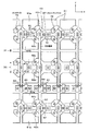
次に、この一実施形態による固体撮像素子における画素内の画素回路の構成図を図2に示す。この例では、4組のフォトダイオード(PD)等より成る受光領域を構成する受光部61(61a〜61d)と転送トランジスタ62(62a〜62d)が、一組のリセットトランジスタ67と増幅トランジスタ64と選択トランジスタ65を共有する例を示す。
光電変換素子であるPD等の受光部61a〜61dは、転送トランジスタ62a〜62dを介してそれぞれフローティングディフュージョン(FD)63と接続されている。FD63は、転送トランジスタ62a〜62dのドレインに相当する2つの拡散層と、増幅トランジスタ64のゲートと、それらを接続する配線から成るノードである。転送トランジスタ62a〜62dは、受光部61a〜61dの光電子をFD63に転送する。増幅トランジスタ64は、ゲートの電圧がFD電圧であるので、FD63の電位に対応した信号を、選択トランジスタ65がONしていれば、垂直信号線68に出力する。リセットトランジスタ67は、FD63の電子を電源(Vdd)配線66に捨てることによって、FD63をリセットする。
Next, FIG. 2 shows a configuration diagram of a pixel circuit in the pixel in the solid-state imaging device according to the embodiment. In this example, a light receiving unit 61 (61a to 61d) and a transfer transistor 62 (62a to 62d) that constitute a light receiving region composed of four sets of photodiodes (PD) and the like are combined into one set of
図2に示す画素回路を平面上にレイアウトした場合の固体撮像素子の構成例を、図3の概略平面構成図に示す。ここでは、見易さのため、FD63の配線69以外の金属配線や、金属配線間のコンタクトを省略している。図3において、図1における行方向を矢印x、列方向を矢印yとして示す。図3に示すように、この場合、一対の受光部61a及び61b、61c及び61d同士が略対称な形状とされて矢印yで示す列方向に配列されて成る。そしてこれらの間にFD63、リセットトランジスタ67やコンタクト部70、また各受光部61a〜61dの転送トランジスタ62a〜62dが配置されるが、これらは受光部61aと61bとの間、受光部61cと61dとの間と、列方向に関して1つおきの受光部間に配置される。この場合、受光部61bと61cとの間隔D1と、受光部61cと61dとの間隔D2とは異なり、すなわち受光部が非等間隔に配列される。
An example of the configuration of the solid-state imaging device when the pixel circuit shown in FIG. 2 is laid out on a plane is shown in a schematic plan configuration diagram of FIG. Here, for the sake of clarity, metal wiring other than the
この画素回路の断面構造を、図4A及びBを参照して説明する。図4Aは、図3に示す概略平面構成図の一部を示し、図4A中線AA’線上の断面構成図を図4Bに示す。図4において、図3と対応する部分には同一符号を付して重複説明を省略する。なお、図4Aにおいては、便宜上図3に示す平面構成図を横に90度回転して示す。図4Bにおいては、配線や支持基板、カラーフィルターやオンチップレンズなどを省略して、シリコン等より成る半導体基体11と転送トランジスタ電極62a〜62dのみ示す。
A cross-sectional structure of the pixel circuit will be described with reference to FIGS. 4A and 4B. 4A shows a part of the schematic plan configuration diagram shown in FIG. 3, and FIG. 4B shows a cross-sectional configuration diagram along the middle line AA ′ in FIG. 4A. In FIG. 4, parts corresponding to those in FIG. In FIG. 4A, for convenience, the plane configuration diagram shown in FIG. In FIG. 4B, wiring, a support substrate, a color filter, an on-chip lens, and the like are omitted, and only the
本発明においては、受光部61a〜61dの深さ方向の形状を、隣接する画素間で異ならせていることに特徴がある。図示の例では、半導体基体11の画素回路を形成する第1の面11A側において非等間隔に、素子分離領域18に隔てられて例えばp型の第2導電型不純物領域21a〜21d及び例えばn型の第1導電型不純物領域20a〜20dが形成される。一方、半導体基体11の画素回路を形成する側とは反対側で、光入射側である第2の面11Bにおいては、略等間隔に、第1導電型不純物領域20a〜20dと接続する例えば比較的低濃度のn − 型の第1導電型不純物領域17a〜17dが形成されて、受光部61a〜61dが構成される。
The present invention is characterized in that the shapes of the
このとき、受光部61a〜61dの第1の面11A側と、第2の面11B側との接合部は、破線Ca〜Cdで囲んで示すように、第1の面11A側における不純物領域の配置位置と、第2の面11B側における不純物領域の配置位置との違いに対応して異なる形状とする。すなわちこの場合、各接合部Ca〜Cdは隣接する画素間で異なる位置及び面積をもった形状となる。いわば半導体基体11の内部で不純物領域をそれぞれ曲げて接続する構成となる。このように接続位置を適切に選定することによって、受光部61a〜61dの配置を、第1の面11A側においては非等間隔でも、光入射面側である第2の面11B側において略等間隔にできて、画素毎の空間的なサンプリングは略等間隔になる。
したがって、従来は画素の特性を犠牲にするか、光の進路を曲げることで解決を図ってきた問題を、本発明では、光電変換された電子の進路を画素毎に異なるように曲げることにより解決するものである。
なお、不純物領域の積層数は図示の例に限定されることはなく、2層でも、また4層以上の構成とすることも可能である。ただし、p型領域とn型領域との接合面は、各画素において略同一形状、同一面積であることが望ましい。また、p型とn型とを逆導電型としてもよい。
At this time, the junction between the
Therefore, in the present invention, the problem that has been solved by sacrificing the characteristics of the pixel or bending the light path is conventionally solved by bending the photoelectrically converted electron path differently for each pixel. To do.
Note that the number of stacked impurity regions is not limited to the illustrated example, and may be two layers or four or more layers. However, it is desirable that the junction surfaces of the p-type region and the n-type region have substantially the same shape and the same area in each pixel. Further, the p-type and the n-type may be reversed conductivity types.
ところで、このように隣接する画素間で受光部の深さ方向の構造が異なる場合は、構造の違いによってシェーディングが新たに発生する可能性がある。すなわち、図4Bにおいて矢印La〜Ldで示すように、第2の面11B側から斜めの角度で光が入射したときに、第1導電型不純物領域17a〜17dと破線Ca〜Cdで囲む接合部との相対的な位置の違いによって、この上の第1導電型不純物領域20a〜20dに光が到達する場合と到達しない場合が生じる恐れがある。図示の例では、領域17c及び17dにおいて矢印Lc及びLdの先端部を破線で示すように、第1導電型不純物領域20c及び20dに到達しない。
このようなばらつきを防ぐには、第2の面11B側に略等間隔に配置する第1導電型不純物領域17a〜17dにおいて十分に光電変換がなされ、多くの光がこの領域17a〜17dを突き抜けないことが重要である。そのため、この第1導電型不純物領域17a〜17dが半導体基体11の深さ方向に、第2の面11Bから1μm以上延在することが望ましい。また、この領域17a〜17dを空乏化させ、光電変換された電子を電界によって第1の面11A側に送るためには、第2の面11Bからの深さが5μm以下であることが望ましい。
By the way, when the structure of the light receiving part in the depth direction is different between adjacent pixels in this way, there is a possibility that shading may newly occur due to the difference in structure. That is, as indicated by arrows La to Ld in FIG. 4B, when light is incident at an oblique angle from the
In order to prevent such variations, sufficient photoelectric conversion is performed in the first conductivity
次に、本発明の一実施形態に係る固体撮像素子の製造方法を、図5〜図9の製造工程図を参照して説明する。図5〜図9においては、図4Bに示す領域の一部分を例に、主要な事項のみを説明する。
(1)この例では、例えば厚膜SOI(Semiconductor On Insulator)基板を用いる場合で、図5Aに示すように、シリコン等より成る基板13上に埋め込み酸化膜等より成る絶縁膜12を介して形成されたシリコン部等を半導体基体11として用いてもよい。すなわち、本発明の固体撮像素子における半導体基体としては、基体の一部に設ける半導体領域でもよい。SOI基板を用いる場合のシリコン部、すなわち半導体基体11の厚さtは、例えば4μm程度と比較的厚いことが望ましく、また不純物濃度は1015cm―3程度という低濃度の第1導電型、例えばn−−型とし得る。
Next, the manufacturing method of the solid-state image sensor which concerns on one Embodiment of this invention is demonstrated with reference to the manufacturing-process figure of FIGS. 5 to 9, only the main items will be described by taking a part of the region shown in FIG. 4B as an example.
(1) In this example, for example, when using a thick film SOI (Semiconductor On Insulator) substrate, as shown in FIG. 5A, it is formed on a
半導体基体11の表面に薄く熱酸化より成る絶縁膜14を形成した後、深さ例えば1.8μm以上の領域に、例えばp型不純物であるボロン等を注入して第2導電型不純物領域15を形成する。このように、表面から比較的深い領域にイオン注入を行う場合は、メガ電子ボルトを扱える高エネルギーのイオン注入装置により行うことが望ましい。この第2導電型不純物領域15は、平面形状を例えば格子状として、それぞれ等間隔に配置して形成する。
After forming a thin insulating
(2)図5Bに示すように、半導体基体11の第1の面11Aから深さ1.8μm以下の領域で、後の工程において受光部の上部となる領域を避けて、ボロン等の第2導電型不純物を注入し、第2導電型不純物領域15に接続する第2導電型不純物領域16を形成する。
第1の面11A側の受光部は非等間隔の配置とするので、上記(1)工程で注入した深い位置の第2導電型不純物領域15との接続部分は、隣接する画素間で形状、すなわち接続位置及び接続面積が異なる。
(2) As shown in FIG. 5B, in a region having a depth of 1.8 μm or less from the
Since the light receiving portions on the
(3)次に、図5Cに示すように、絶縁膜14に至らない程度の深さ、すなわち第1の面11Aから約1.8μm以上3.5μm以下程度の深さの領域に、受光部の下部となる例えばn型の第1導電型不純物のイオン注入を行って、n−型の第1導電型不純物領域17を形成する。この場合においても、上述の第2導電型不純物領域15と同様に、メガ電子ボルトを扱える高エネルギーのイオン注入装置を使って不純物注入を行う。
このイオン注入は、上記(1)工程において第2導電型不純物領域15を格子状としたその開口部分に注入し、したがって、この第1導電型不純物領域17は互いに等間隔の配置となる。
(3) Next, as shown in FIG. 5C, a light receiving portion is formed in a region not reaching the insulating
This ion implantation is performed in the opening portion of the second conductivity
しかしながらこの場合、第1の面11A側の画素の構成は隣接画素間で異なるので、イオン注入による表面付近へのダメージも隣接画素間で異なる。このダメージの程度の隣接画素間差を小さくするように、イオン種として原子量の小さい例えばリンを用いることが望ましい。
However, in this case, since the configuration of the pixels on the
一方、電子を受光部の第1の面11A側、すなわち配線回路側に収集するためには、第1の面11A側ほど不純物濃度が濃いように構成するのが好ましい。そのために、数回に渡って第1の面11A側ほどドーズ量を増やしてイオン注入することが好適である。
On the other hand, in order to collect electrons on the
ここで、このような深い領域へのイオン注入は、後で第2の面11Bすなわち裏面側を露出してから、この裏面側からより低いエネルギーで注入するという方法も考えられる。しかしながら、本実施の形態においては、上記(3)工程において、第1の面11A側すなわち半導体基体の表面側から高いエネルギーでイオン注入を行う。その理由は以下の通りである。
Here, for such ion implantation into a deep region, a method may be considered in which the
本発明による固体撮像素子においては、隣接画素間で受光部の第1の面側と第2の面側との接続位置が異なる。このため、リン等の不純物濃度に局所的な濃淡があると、感度や飽和や残像などに隣接画素間でばらつきが生じる恐れがある。このばらつきを回避又は抑制するには、局所的な濃淡が少なくなだらかな濃度分布になるように、イオン注入の後で比較的多めに拡散させることが望ましい。そのためには比較的強い熱工程を加えることとなるが、そのような熱工程をかけると他のイオンも拡散してしまうので、まだ細かな形状が形成されていない素子分離領域の形成前に、裏面側すなわち第2の面11B側の受光部のイオン注入工程を行うことが望ましいこととなる。
このとき、後の素子分離領域形成のために行う比較的強い熱工程を、第2の面11B側の第1導電型不純物領域17の不純物の拡散に使うことができ、工程追加を防止できるという利点もある。
In the solid-state imaging device according to the present invention, the connection positions of the first surface side and the second surface side of the light receiving unit are different between adjacent pixels. For this reason, if there is local shading in the impurity concentration of phosphorus or the like, there is a possibility that variations in sensitivity, saturation, afterimage, etc. occur between adjacent pixels. In order to avoid or suppress this variation, it is desirable to diffuse a relatively large amount after ion implantation so that the local density is small and the density distribution is gentle. For that purpose, a relatively strong thermal process is applied, but when such a thermal process is applied, other ions also diffuse, so before forming the element isolation region where the fine shape has not yet been formed, It is desirable to perform the ion implantation process of the light receiving portion on the back surface side, that is, the
At this time, a relatively strong thermal process performed for the subsequent element isolation region formation can be used for the diffusion of the impurity in the first conductivity
また、この工程で注入するということは、必然的に第1の面11A側から注入することとなる。上記(1)〜(3)工程では、いずれも最終的な出来上がりよりもやや狭い面積にイオン注入しておき、後の素子分離領域形成のための熱工程による拡散で、分布が緩やかに重なり合うようにしている。これにより、水平方向にも緩やかな濃度勾配が生まれ、電子を第1の面11A側の受光部に移動しやすくなる。
更にまた、第1の面11Aから不純物を注入する場合に、素子分離形成より後に注入すると、素子分離領域を通過する部分と素子分離領域以外を通過する部分とにおいて、注入深さが異なってしまう。画素が全て同じレイアウトであれば問題は小さいが、本発明の固体撮像素子におけるように、画素共有型の回路構成とする場合においては、隣接画素のレイアウトすなわち配置構成が異なるので、上述したようなイオン注入深さのばらつきは、感度や飽和特性などに隣接画素間差が起こる原因になる。したがって、第1の面11A側から注入する場合は、この理由によっても、素子分離領域の形成前に行うことが好ましいといえる。
In addition, injecting in this step necessarily means injecting from the
Furthermore, when the impurity is implanted from the
(4)次に、図6Aに示すように、素子分離領域18を形成する。ここではSTI(Shallow Trench Isolation)を用いている。これは、シリコン等の半導体基体11に穴を掘り、その穴を例えばSiO2で埋め込むことによる素子分離である。途中950℃程度の強い熱工程を通すので、上述したように、前の工程で注入したイオンが多めに拡散する。
(5)その後、図6Bに示すように、絶縁層14を介して、ゲート電極19を形成する。
(4) Next, as shown in FIG. 6A, an
(5) Thereafter, as shown in FIG. 6B, a
(6)図6Cに示すように、受光部の第1の面11A側の構造を形成する。例えば、第1導電型この場合n型のヒ素等をイオン注入して、第1導電型不純物領域20を形成する。そして、図示しないがゲート電極19の側壁を形成し、第2導電型この場合p型のボロン等をイオン注入し、850℃程度の軽い熱工程を通してあまり拡散させずに活性化する。図示しないが、トランジスタのソース・ドレインもこの工程位置にて形成する。
(6) As shown in FIG. 6C, a structure on the
(7)図7に示すように、ゲート電極19上に層間絶縁層22を介して配線層23、24を形成し、BCB(ベンゾシクロブテン)樹脂などの接着剤31により、シリコン等の支持基板32を貼り付ける。
(8)その後、半導体基体11すなわちSOI基板を裏返し、SOIの基板13と埋め込み酸化膜より成る絶縁層12を研磨とエッチングにて除去し、第2の面11Bを露出する。更に、第2の面11Bの表面に薄い保護酸化膜を形成し、図8に示すように、第2の面11B側表面にボロン等をイオン注入し、レーザーアニール等で活性化してp型の第2導電型不純物層26を形成する。更にこの上に酸化膜40を積層形成する。
(9)その後、図9に示すように、第2の面11B上の酸化膜40上にシリコン窒化膜等より成る保護膜41を形成し、更に、カラーフィルター42とオンチップレンズ43を形成する。これらカラーフィルター42及びオンチップレンズ43は、受光部を構成する第2導電型不純物領域21、第1導電型不純物領域20及び17に対応する位置に、略等間隔に形成する。
(7) As shown in FIG. 7, wiring layers 23 and 24 are formed on the
(8) Thereafter, the
(9) Thereafter, as shown in FIG. 9, a
ここで、本発明において等間隔というのは、完全厳密に等間隔でなくとも、実用上問題のないレベルであればよく、より具体的には、受光部の間隔のばらつきを補正する特別な信号処理を不要とすることができる範囲であればよい。 Here, the equal interval in the present invention may be a level that does not cause any practical problem even if it is not exactly equal, and more specifically, a special signal for correcting the variation in the interval between the light receiving portions. It may be in a range where processing can be made unnecessary.
また、本発明の固体撮像素子においては、受光部の第1の面側と第2の面側、すなわち表側と裏側とで配置が異なるわけであるが、その相対的な位置関係として最適な配置を選定することが望ましい。一例として、上述の実施形態例のように、4画素単位の繰り返しになっている場合は、以下の方法を用いて選定することができる。
表面側の受光部例えばPDの幾何重心が、座標軸上の点p1、p2、p3、p4の位置に非等間隔に並んでおり、裏面側ではPDの幾何重心を等間隔に、座標軸上の点q1、q2、q3、q4に等間隔に並べるとする。このとき、表面側と裏面側との相対関係を決めるのには、p1−q1、p2−q2、p3−q3、p4−q4のうち最大値pi−qiと最小値pj−qjが、(i,jはそれぞれ1〜4のどれか)、
pi−qi=−(pj−qj)
となるようにするとよい。これは、PDの表面側と裏面側の間での幾何重心のずれの最大値を最小にするということでもある。
図4Bの例では、受光部61bと61cが、幾何重心のずれの最大値と最小値を与え、受光部61aと61dは、その間の値をとっている。受光部61bと61cは、左右を反転すれば同じ形状になるが、そのままでは入射光LbとLcに対する形状が異なるので、ここでは異なる形状である。
なお、4画素単位の繰り返し以外の場合にも、この方法を適用できることは自明である。
Further, in the solid-state imaging device of the present invention, the arrangement differs between the first surface side and the second surface side of the light receiving unit, that is, the front side and the back side. It is desirable to select As an example, when the repetition is made in units of four pixels as in the above-described embodiment, selection can be made using the following method.
On the front side, for example, the geometric center of gravity of the PD is arranged at non-equal intervals at the positions of points p1, p2, p3, and p4 on the coordinate axis, and on the back side, the geometric center of gravity of the PD is equally spaced and the point on the coordinate axis Assume that q1, q2, q3, and q4 are arranged at equal intervals. At this time, the maximum value pi-qi and the minimum value pj-qj out of p1-q1, p2-q2, p3-q3, and p4-q4 are determined by (i , J is any one of 1-4)
pi-qi =-(pj-qj)
It is recommended that This also means minimizing the maximum deviation of the geometric center of gravity between the front side and the back side of the PD.
In the example of FIG. 4B, the
It is obvious that this method can be applied to cases other than the repetition of 4 pixel units.
ここまで列方向の4画素を共有する構成とする例で説明したが、画素の共有方法は他にも種々の構成が提案されている。例えば図10に示すように、列方向に隣接する2画素を共有する構成や、図11に示すように、列方向及び行方向に2画素ずつ、すなわち2行2列の4画素を共有する構成もある。図10及び図11において、図3と対応する部分には同一符号を付して重複説明を省略する。本発明は、これらを始め、各種の複数の画素に対して画素回路を共有する固体撮像素子に対して同様に適用できる。なお、図10に示す例においては、配線69を受光部上にも通しているが、本発明の固体撮像素子は裏面入射型構成とするので、問題ない。従来の表面入射型構成とする場合では、入射光の邪魔になるので、このようにPD上を配線が横切る構成とすることはできないが、裏面入射型構成とすることによって、このように配線の配置位置の自由度を高めることができるので、より画素及び回路構成の微細化が可能となる。
The example in which the four pixels in the column direction are shared has been described so far, but various other configurations of pixel sharing methods have been proposed. For example, as shown in FIG. 10, a configuration sharing two pixels adjacent in the column direction, or a configuration sharing two pixels in the column direction and the row direction, that is, four pixels in two rows and two columns, as shown in FIG. There is also. 10 and 11, parts corresponding to those in FIG. In addition to these, the present invention can be similarly applied to a solid-state imaging device that shares a pixel circuit for various types of pixels. In the example shown in FIG. 10, the
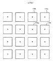
上述の本発明の一実施形態に係る固体撮像素子における裏面すなわち第2の面11B側から見た受光部の平面構成図を図12に示す。図12に示すように、この場合、受光部61の入射側領域である第1導電型不純物領域17は、略等間隔に配置される。一例として、緑G、赤R及び青Bとして、単板式カメラ用のカラー固体撮像装置における各色のカラーフィルターに対応する第1導電型不純物領域17の配置例を図12に示す。
FIG. 12 is a plan configuration diagram of the light receiving unit viewed from the back surface, that is, the
上述したように、本発明の固体撮像素子において、第2の面側すなわち裏面側の受光部を略等間隔とするとは、完全厳密に等間隔でなくとも、実用上問題のない範囲であればよい。すなわち、微妙に間隔が異なっても、後段の信号処理で、サンプリングが等間隔であると扱えるレベルであれば問題ない。 As described above, in the solid-state imaging device according to the present invention, the light receiving portions on the second surface side, that is, the back surface side are set at substantially equal intervals, as long as they are not strictly equal intervals but are in a range that does not cause any practical problems. Good. That is, even if the intervals are slightly different, there is no problem as long as the level is such that sampling can be handled at equal intervals in the subsequent signal processing.
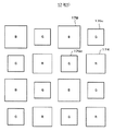
また、裏面側の受光部61、すなわち第1導電型不純物領域17の形状や面積は、全て等しいことが好ましいが、等間隔に並んでいれば、形状や面積が必ずしも全部同じである必要はない。
例えば、図13においては、裏面側からpウェル等にコンタクトを落とすことを想定してコンタクト部70を第1導電型不純物領域17の間に配置する構成としており、この第1導電型不純物領域17の一部が欠けた平面形状とする例を示す。このような平面形状とする場合は重心の位置が厳密には等間隔でなくなる。しかしながらこのような構成とする場合でも、後段の信号処理でサンプリングが等間隔であると扱えるレベルであればよい。
Moreover, it is preferable that the shape and area of the
For example, in FIG. 13, the
また例えば、分光感度を揃えるために、図14に示すように、カラーフィルターの位置に対応して裏面側の第1導電型不純物領域17の面積を異ならせることも可能である。図14に示す例においては、それぞれの面積は違うが、重心の位置は等間隔に並んでいる。
例えば青感度がとりにくいときに、図14に示すように、青のカラーフィルターに対応する受光部61、この場合第1導電型不純物領域17Bのみ面積を大きめに作製することにより、青感度を高めることが可能となる。
Further, for example, in order to make the spectral sensitivities uniform, as shown in FIG. 14, the area of the first conductivity
For example, when the blue sensitivity is difficult to obtain, as shown in FIG. 14, the blue sensitivity is increased by making the
以上説明した本発明の実施形態に係る固体撮像素子を用いて、図15に示すように、本発明構成の撮像装置100を作製することができる。
図15に示す撮像装置100は、携帯電話、デジタルスチルカメラ、ビデオカメラ、その他の撮像機能を有する電子機器として構成される。撮像装置100は、撮像光学部101、固体撮像素子102、信号処理部103、また例えばこの信号処理部103と伝送バスライン104によって接続される一時記憶部105、表示部106、記憶部107、操作部108及び電源部109によって構成される。
Using the solid-state imaging device according to the embodiment of the present invention described above, an
An
撮像光学部101は、各種レンズ、シャッター、絞り機構等からなり、被写体画像を固体撮像素子102に導く。固体撮像素子102は、上述の実施の形態の固体撮像素子であり、撮像光学部101を通して結像された被写体光を光電変換することにより、信号として出力する。信号処理部103は、デジタル信号を処理するDSP(Digital Signal Processors)等で構成され、固体撮像素子102から出力された画像信号にフォーマット等の処理を施し、表示用や記録用のデータに変換する。
The imaging
一時記憶部105は、RAM(Random Access Memory)等によって構成され、信号処理部103によって処理された画像データを一時的に記録する。表示部106は、液晶表示器等によって構成され、上記信号処理部103で処理した画像データを表示する。記録部107は、フラッシュメモリ、EPROM(Erasable Programmable ROM)、HD(ハードディスク)等により構成され、画像データを記録する。操作部108は、撮像装置100の動作を制御する制御信号を外部から入力するシャッタボタン、各種機能キー、カーソルキー等により構成される。電源部109は、撮像装置100の上記各部に動作電源を供給する。
The
撮像装置100を上述の実施の形態の固体撮像素子を用いて構成することにより、等間隔サンプリングによる信号処理を行うことができるので、信号処理の煩雑化を回避することができる。
なお、撮像装置100は上述の構成に限られず、その他の様々な構成によって形成することができる。
By configuring the
Note that the
以上説明したように、本発明の固体撮像素子及び撮像装置によれば、複数の画素に対して共通の画素回路を設けることによって、画素の微細化したがって画素数の増大化を図りつつ、裏面入射型として裏面側で略等間隔の受光部の配置とすることによって、入射光を等間隔でサンプリングできる。
信号処理部例えばDSPの選択の幅が広く、かつ、シェーディング補正やその他信号処理の煩雑化を回避できる。この結果、信号処理が軽くて画像がきれいである。また、等間隔サンプリングのために画素の特性を落としていないので、比較的綺麗な画像を撮像することができる。
As described above, according to the solid-state imaging device and imaging apparatus of the present invention, by providing a common pixel circuit for a plurality of pixels, the back surface incidence is achieved while miniaturizing the pixels and thus increasing the number of pixels. Incident light can be sampled at equal intervals by arranging the light receiving portions at substantially equal intervals on the back side as a mold.
A signal processing unit such as a DSP has a wide selection range, and shading correction and other complications of signal processing can be avoided. As a result, the signal processing is light and the image is clean. Also, since the characteristics of the pixels are not deteriorated for sampling at equal intervals, a relatively clean image can be taken.
画素共有のレイアウトで、PDが非等間隔になっても、等間隔で入射光をサンプリングできる。
それにより、非等間隔とする従来の固体撮像素子に対して、次の利点が得られる。
a.信号処理が簡明であり、結果的に比較的きれいな画像を提供できる。
b.CMOSセンサの製品ごとに、信号処理部例えばDSPのシステムを設計する必要がなく、画素の配置によって信号処理部のシステムを異ならせる必要がない。
c.縞模様を撮影した場合の、縞の間隔や色のつき方の再現性が良好である。
d.多くの信号処理ICを選択肢にもてるため、装置の構成方法が多様となる。
e.入射受光部の非等間隔性に起因して、シェーディングの出方が異なることがない。例えば、白いものを写したときに、上端と下端で、色がつき、しかも異なる色が付いて補正が困難となることがなく、信号処理の煩雑化を回避できる。
With the pixel sharing layout, even if the PDs are not evenly spaced, incident light can be sampled at evenly spaced intervals.
Thereby, the following advantages can be obtained with respect to the conventional solid-state imaging device having non-equal intervals.
a. Signal processing is simple, and as a result, a relatively clean image can be provided.
b. There is no need to design a signal processing unit such as a DSP system for each CMOS sensor product, and there is no need to make the signal processing unit system different depending on the pixel arrangement.
c. The reproducibility of the stripe spacing and coloration when shooting a striped pattern is good.
d. Since many signal processing ICs can be selected, there are various methods for configuring the apparatus.
e. There is no difference in the appearance of shading due to the non-uniform spacing of the incident light receiving portions. For example, when a white object is copied, the upper end and the lower end are colored, and different colors are not attached to make correction difficult, thereby avoiding complication of signal processing.
また、従来の固体撮像素子において、画素回路の共有化と受光部が非等間隔であることによる不都合を解決する方法に対して、本発明による場合は、下記の効果を奏する。
f.開口形状に制限を設ける必要がなく、受光部の面積を低減化することを回避できる。
g.変換ゲインなど画素回路の特性を低下させることを回避できる。
h.受光部の面積を表面入射型と比べて確保できるので、感度の低下を回避できる。
i.画素サイズが異なるCMOSセンサ等の固体撮像素子を新たに設計するたびに、屈折率の異なる材料を選びなおすとか、層内レンズの形状を設計しなおすなどの作業が必要であったが、このような煩雑な作業が不要となる。
In addition, in the conventional solid-state imaging device, the present invention has the following effects as compared with the method for solving the inconvenience caused by the sharing of the pixel circuits and the non-uniform spacing of the light receiving portions.
f. There is no need to limit the shape of the opening, and it is possible to avoid reducing the area of the light receiving portion.
g. Degradation of pixel circuit characteristics such as conversion gain can be avoided.
h. Since the area of the light receiving portion can be ensured as compared with the front-illuminated type, a decrease in sensitivity can be avoided.
i. Every time a new solid-state imaging device such as a CMOS sensor with a different pixel size was designed, it was necessary to reselect materials with different refractive indexes or redesign the shape of the inner lens. Troublesome work becomes unnecessary.
なお、本発明は上述の実施形態例において説明した構成に限定されるものではなく、その他本発明構成を逸脱しない範囲において種々の変形、変更が可能である。 The present invention is not limited to the configuration described in the above-described embodiment, and various modifications and changes can be made without departing from the configuration of the present invention.
1.画素部、2.垂直駆動回路、3.カラム部、4.水平駆動回路、5.制御回路、6.水平バス、7.出力回路、10.固体撮像素子、11.半導体基体、12.絶縁膜、13.基板、14.絶縁膜、15.第2導電型不純物領域、16.第2導電型不純物領域、17.第1導電型不純物領域、18.素子分離領域、19.ゲート電極、20.第1導電型不純物領域、21.第2導電型不純物領域、61.受光部、62.転送トランジスタ、63.フローティングディフュージョン、64.増幅トランジスタ、65.選択トランジスタ、66.電源、67.リセットトランジスタ、100.撮像装置、101.撮像光学部、102.固体撮像素子、103.信号処理部、104.伝送バスライン、105.一時記憶部、106.表示装置、107.記録装置、108.操作部、109.電源部
1. Pixel unit, 2. 2. vertical drive circuit; Column part, 4. 4. Horizontal drive circuit, Control circuit, 6. 6. Horizontal bus, Output circuit, 10. 10. solid-state image sensor; A semiconductor substrate, 12. 12. insulating film; Substrate, 14. 15. insulating film; Second impurity region of second conductivity type, 16. A second conductivity type impurity region; First conductivity type impurity region, 18. Element isolation region, 19. Gate electrode, 20. 20. first conductivity type impurity region; Second conductivity type impurity region, 61. Light receiving unit, 62. Transfer transistor, 63. Floating diffusion, 64. Amplification transistor, 65. Selection transistor, 66. Power supply, 67. Reset transistor, 100. Imaging apparatus, 101. Imaging optical unit, 102. Solid-state image sensor, 103. Signal processing unit, 104. Transmission bus line, 105.
Claims (11)
前記第1の面に形成された前記画素回路が複数の前記受光領域に対応して共有され、
前記受光領域が、前記第2の面側において略等間隔に配置される不純物領域と、前記第1の面側において非等間隔に配置される不純物領域とを有し、前記半導体基体中で前記第2の面側の不純物領域と前記第1の面側の不純物領域とを接続する形状で前記第2の面側から前記第1の面側に延在されて成り、隣接する前記受光領域間で断面形状が異なる
固体撮像素子。 The light incident side of the light receiving region is a second surface side opposite to the first surface on which the pixel circuit of the semiconductor substrate is formed,
The pixel circuit formed on the first surface is shared corresponding to the plurality of light receiving regions,
The light receiving region, the impurity region that will be placed at approximately equal intervals in the second surface, and a first impurity region in the side that will be placed in the non-equal intervals, said in said semiconductor body second impurity regions of the surface side to the first Ri formed from the second surface in a shape for connecting the impurity region of the surface side is extended on the first surface, the light receiving regions adjacent Solid-state image sensors with different cross-sectional shapes .
請求項1記載の固体撮像素子。The solid-state imaging device according to claim 1.
請求項1または2記載の固体撮像素子。The solid-state imaging device according to claim 1 or 2.
前記第2の面側の不純物領域は、前記第1導電型不純物領域と接続すると共に当該第1導電型不純物領域よりも低濃度な第1導電型の不純物領域で構成されるThe impurity region on the second surface side is connected to the first conductivity type impurity region and is composed of a first conductivity type impurity region having a lower concentration than the first conductivity type impurity region.
請求項1〜3の何れか記載の固体撮像素子。The solid-state image sensor in any one of Claims 1-3.
請求項4記載の固体撮像素子。The solid-state imaging device according to claim 4.
請求項1〜5の何れか記載の固体撮像素子。The solid-state image sensor in any one of Claims 1-5.
請求項1〜6の何れか記載の固体撮像素子。The solid-state image sensor in any one of Claims 1-6.
請求項1〜7の何れか記載の固体撮像素子。 Wherein the light receiving region, the depth of the impurity region of the second surface side, the solid-state imaging device according to any one of claims 1 to 7, wherein the from the second surface of the semiconductor substrate and 1μm or 5μm or less.
前記固体撮像素子は、
受光領域の光入射側が、半導体基体の画素回路が形成される第1の面とは反対側の第2の面側とされ、
前記第1の面に形成された前記画素回路が複数の前記受光領域に対応して共有され、
前記受光領域が、前記第2の面側において略等間隔に配置される不純物領域と、前記第1の面側において非等間隔に配置される不純物領域とを有し、前記半導体基体中で前記第2の面側の不純物領域と前記第1の面側の不純物領域とを接続する形状で前記第2の面側から前記第1の面側に延在されて成り、隣接する前記受光領域間で断面形状が異なる
固体撮像装置。 An imaging apparatus comprising: an imaging optical unit; a solid-state imaging device; and a signal processing unit that processes an image signal output from the solid-state imaging device,
The solid-state imaging device is
The light incident side of the light receiving region is a second surface side opposite to the first surface on which the pixel circuit of the semiconductor substrate is formed,
The pixel circuit formed on the first surface is shared corresponding to the plurality of light receiving regions,
The light receiving region, the impurity region that will be placed at approximately equal intervals in the second surface, and a first impurity region in the side that will be placed in the non-equal intervals, said in said semiconductor body second impurity regions of the surface side to the first Ri formed from the second surface in a shape for connecting the impurity region of the surface side is extended on the first surface, the light receiving regions adjacent Solid-state imaging devices with different cross-sectional shapes .
前記第1の面側に素子分離領域を形成する工程と、
前記第1の面上に、複数の前記受光領域に対応して共有される画素回路を構成するゲート電極を形成する工程と、
隣接する前記受光領域間で異なる断面形状で前記受光領域の第2の面側の不純物領域と接続するように、前記第1の面側から不純物を注入して、前記半導体基体の前記第1の面側の部分に非等間隔に前記受光領域の第1の面側の不純物領域を形成する工程とを有し、
前記素子分離領域を形成する工程の前に、前記第1の面側から不純物を注入して前記受光領域の第2の面側の不純物領域を形成する工程を行う
固体撮像素子の製造方法。 By implanting a first surface side or found not pure product of the semiconductor substrate, the second surface of the first surface receiving regions at approximately equal intervals on the second surface side of the portion opposite to the semiconductor substrate Forming a side impurity region;
Forming an element isolation region on the first surface side;
Forming on the first surface a gate electrode constituting a pixel circuit shared corresponding to the plurality of light receiving regions ;
So as to be connected to the second surface of the impurity region of the light receiving region in a different cross-sectional shapes between the light receiving regions adjacent to injecting the first surface or found not pure products, the said semiconductor body and a step of forming an impurity region of the first surface of the light receiving region to the non-equal intervals in the portion of the first surface,
Production method of the prior step of forming an element isolation region, said first solid-state imaging device by injecting an impurity from the surface side a step of forming an impurity region of the second surface of the light receiving region.
請求項10記載の固体撮像素子の製造方法。The manufacturing method of the solid-state image sensor of Claim 10.
Priority Applications (17)
| Application Number | Priority Date | Filing Date | Title |
|---|---|---|---|
| JP2007138081A JP5104036B2 (en) | 2007-05-24 | 2007-05-24 | Solid-state imaging device, manufacturing method thereof, and imaging apparatus |
| TW097115749A TWI369781B (en) | 2007-05-24 | 2008-04-29 | Solid-state imaging device, production method of the same, and imaging apparatus |
| US12/124,496 US7884436B2 (en) | 2007-05-24 | 2008-05-21 | Solid-state imaging device, production method of the same, and imaging apparatus |
| KR1020080048104A KR101534116B1 (en) | 2007-05-24 | 2008-05-23 | Solid-state imaging device |
| CN2008101088103A CN101312204B (en) | 2007-05-24 | 2008-05-26 | Solid-state imaging device, production method thereof and imaging device |
| US12/852,747 US8173479B2 (en) | 2007-05-24 | 2010-08-09 | Solid-state imaging device, production method of the same, and imaging apparatus |
| US13/438,425 US8497561B2 (en) | 2007-05-24 | 2012-04-03 | Solid-state imaging device, production method of the same, and imaging apparatus |
| US13/928,915 US8749008B2 (en) | 2007-05-24 | 2013-06-27 | Solid-state imaging device, production method of the same, and imaging apparatus |
| US14/257,644 US9281337B2 (en) | 2007-05-24 | 2014-04-21 | Solid-state imaging device, production method of the same, and imaging apparatus |
| KR1020140051691A KR101541120B1 (en) | 2007-05-24 | 2014-04-29 | Imaging device |
| US14/317,881 US8896036B2 (en) | 2007-05-24 | 2014-06-27 | Solid-state imaging device, production method of the same, and imaging apparatus |
| US14/453,298 US9455296B2 (en) | 2007-05-24 | 2014-08-06 | Solid-state imaging device, production method of the same, and imaging apparatus |
| US15/272,234 US9635294B2 (en) | 2007-05-24 | 2016-09-21 | Solid-state imaging device, production method of the same, and imaging apparatus |
| US15/454,290 US9899435B2 (en) | 2007-05-24 | 2017-03-09 | Solid-state imaging device, production method of the same, and imaging apparatus |
| US15/887,770 US10141355B2 (en) | 2007-05-24 | 2018-02-02 | Solid-state imaging device, production method of the same, and imaging apparatus |
| US16/199,529 US10304879B2 (en) | 2007-05-24 | 2018-11-26 | Solid-state imaging device, production method of the same, and imaging apparatus |
| US16/398,854 US10685996B2 (en) | 2007-05-24 | 2019-04-30 | Solid-state imaging device, production method of the same, and imaging apparatus |
Applications Claiming Priority (1)
| Application Number | Priority Date | Filing Date | Title |
|---|---|---|---|
| JP2007138081A JP5104036B2 (en) | 2007-05-24 | 2007-05-24 | Solid-state imaging device, manufacturing method thereof, and imaging apparatus |
Publications (3)
| Publication Number | Publication Date |
|---|---|
| JP2008294218A JP2008294218A (en) | 2008-12-04 |
| JP2008294218A5 JP2008294218A5 (en) | 2010-01-28 |
| JP5104036B2 true JP5104036B2 (en) | 2012-12-19 |
Family
ID=40100724
Family Applications (1)
| Application Number | Title | Priority Date | Filing Date |
|---|---|---|---|
| JP2007138081A Active JP5104036B2 (en) | 2007-05-24 | 2007-05-24 | Solid-state imaging device, manufacturing method thereof, and imaging apparatus |
Country Status (5)
| Country | Link |
|---|---|
| US (12) | US7884436B2 (en) |
| JP (1) | JP5104036B2 (en) |
| KR (2) | KR101534116B1 (en) |
| CN (1) | CN101312204B (en) |
| TW (1) | TWI369781B (en) |
Families Citing this family (76)
| Publication number | Priority date | Publication date | Assignee | Title |
|---|---|---|---|---|
| JP2502098B2 (en) * | 1987-08-12 | 1996-05-29 | 株式会社フジクラ | Superconducting magnetic shield |
| JP5104036B2 (en) | 2007-05-24 | 2012-12-19 | ソニー株式会社 | Solid-state imaging device, manufacturing method thereof, and imaging apparatus |
| JP4998092B2 (en) * | 2007-05-31 | 2012-08-15 | 富士通セミコンダクター株式会社 | Solid-state imaging circuit and camera system |
| US8896712B2 (en) | 2007-07-20 | 2014-11-25 | Omnivision Technologies, Inc. | Determining and correcting for imaging device motion during an exposure |
| US7990445B2 (en) * | 2008-05-30 | 2011-08-02 | Omnivision Technologies, Inc. | Image sensor having differing wavelength filters |
| US8350952B2 (en) | 2008-06-04 | 2013-01-08 | Omnivision Technologies, Inc. | Image sensors with improved angle response |
| EP2133918B1 (en) * | 2008-06-09 | 2015-01-28 | Sony Corporation | Solid-state imaging device, drive method thereof and electronic apparatus |
| US8207590B2 (en) * | 2008-07-03 | 2012-06-26 | Samsung Electronics Co., Ltd. | Image sensor, substrate for the same, image sensing device including the image sensor, and associated methods |
| JP5217792B2 (en) * | 2008-08-29 | 2013-06-19 | 富士通株式会社 | Optical receiver power supply control method, digital signal processing circuit, and optical receiver |
| TWI433307B (en) | 2008-10-22 | 2014-04-01 | Sony Corp | Solid state image sensor, method for driving a solid state image sensor, imaging apparatus, and electronic device |
| JP5012782B2 (en) * | 2008-12-12 | 2012-08-29 | ソニー株式会社 | Imaging device |
| JP5444694B2 (en) * | 2008-11-12 | 2014-03-19 | ソニー株式会社 | Solid-state imaging device, manufacturing method thereof, and imaging device |
| US7902618B2 (en) * | 2008-11-17 | 2011-03-08 | Omni Vision Technologies, Inc. | Backside illuminated imaging sensor with improved angular response |
| US20100133638A1 (en) * | 2008-12-01 | 2010-06-03 | Samsung Electronics Co., Ltd. | Image sensors and methods of manufacturing the same |
| KR101545630B1 (en) * | 2008-12-26 | 2015-08-19 | 주식회사 동부하이텍 | Method for Manufacturing Back Side Illumination Image Sensor |
| KR20100076525A (en) * | 2008-12-26 | 2010-07-06 | 주식회사 동부하이텍 | Method for manufacturing back side illumination image sensor |
| JP5029624B2 (en) * | 2009-01-15 | 2012-09-19 | ソニー株式会社 | Solid-state imaging device and electronic apparatus |
| JP5458582B2 (en) * | 2009-01-28 | 2014-04-02 | ソニー株式会社 | Solid-state imaging device, driving method of solid-state imaging device, and electronic apparatus |
| WO2010090166A1 (en) * | 2009-02-04 | 2010-08-12 | 株式会社 Rosnes | Solid-state image pickup device |
| JP2010225818A (en) * | 2009-03-23 | 2010-10-07 | Toshiba Corp | Solid-state image pickup device and method for manufacturing the same |
| JP5517503B2 (en) * | 2009-06-24 | 2014-06-11 | キヤノン株式会社 | Solid-state imaging device |
| US20100327389A1 (en) * | 2009-06-26 | 2010-12-30 | Mccarten John P | Back-illuminated image sensors having both frontside and backside photodetectors |
| US8076746B2 (en) * | 2009-06-26 | 2011-12-13 | Omnivision Technologies, Inc. | Back-illuminated image sensors having both frontside and backside photodetectors |
| US8018016B2 (en) * | 2009-06-26 | 2011-09-13 | Omnivision Technologies, Inc. | Back-illuminated image sensors having both frontside and backside photodetectors |
| JP5471117B2 (en) | 2009-07-24 | 2014-04-16 | ソニー株式会社 | Solid-state imaging device, manufacturing method thereof, and camera |
| US8405751B2 (en) * | 2009-08-03 | 2013-03-26 | International Business Machines Corporation | Image sensor pixel structure employing a shared floating diffusion |
| WO2011030413A1 (en) * | 2009-09-09 | 2011-03-17 | 株式会社 東芝 | Solid-state image pickup device and method for manufacturing same |
| JP5564874B2 (en) | 2009-09-25 | 2014-08-06 | ソニー株式会社 | Solid-state imaging device and electronic apparatus |
| JP5564909B2 (en) | 2009-11-30 | 2014-08-06 | ソニー株式会社 | SOLID-STATE IMAGING DEVICE, ITS MANUFACTURING METHOD, AND ELECTRONIC DEVICE |
| JP2011114324A (en) | 2009-11-30 | 2011-06-09 | Sony Corp | Solid-state imaging device and electronic apparatus |
| JP5546222B2 (en) * | 2009-12-04 | 2014-07-09 | キヤノン株式会社 | Solid-state imaging device and manufacturing method |
| JP5454894B2 (en) * | 2009-12-16 | 2014-03-26 | 株式会社東芝 | Solid-state imaging device and manufacturing method thereof |
| JP5509846B2 (en) * | 2009-12-28 | 2014-06-04 | ソニー株式会社 | SOLID-STATE IMAGING DEVICE, ITS MANUFACTURING METHOD, AND ELECTRONIC DEVICE |
| JP5537172B2 (en) * | 2010-01-28 | 2014-07-02 | ソニー株式会社 | Solid-state imaging device and electronic apparatus |
| US8319306B2 (en) * | 2010-02-01 | 2012-11-27 | Himax Technologies Limited | Method of fabricating image sensor and image sensor thereof |
| JP5644177B2 (en) | 2010-05-07 | 2014-12-24 | ソニー株式会社 | Solid-state imaging device, manufacturing method thereof, and electronic apparatus |
| KR101738532B1 (en) * | 2010-05-25 | 2017-05-22 | 삼성전자 주식회사 | A Backside Illumination Image Sensor Including an Upper High-doped Region and a Method of Fabricating the Same |
| JP5126291B2 (en) | 2010-06-07 | 2013-01-23 | 株式会社ニコン | Solid-state image sensor |
| JP2012015274A (en) | 2010-06-30 | 2012-01-19 | Canon Inc | Solid-state imaging apparatus, and method of manufacturing the same |
| KR101803719B1 (en) | 2010-10-26 | 2017-12-04 | 삼성전자 주식회사 | Backside illuminated active pixel sensor array and method for manufacturing the same, backside illuminated image sensor with the same |
| JP6299058B2 (en) * | 2011-03-02 | 2018-03-28 | ソニー株式会社 | Solid-state imaging device, method for manufacturing solid-state imaging device, and electronic apparatus |
| JP5358747B2 (en) * | 2011-03-25 | 2013-12-04 | 富士フイルム株式会社 | Back-illuminated solid-state imaging device, manufacturing method thereof, and imaging apparatus |
| TWI415253B (en) | 2011-05-17 | 2013-11-11 | Novatek Microelectronics Corp | Optical sensor and manufacturing method of the same |
| JP6003291B2 (en) * | 2011-08-22 | 2016-10-05 | ソニー株式会社 | Solid-state imaging device and electronic apparatus |
| JP2013187360A (en) | 2012-03-08 | 2013-09-19 | Sony Corp | Solid-state image pickup device and electronic apparatus |
| US20130300902A1 (en) * | 2012-03-29 | 2013-11-14 | Hiok Nam Tay | Color image sensor pixel array |
| SG195515A1 (en) * | 2012-06-11 | 2013-12-30 | Ultratech Inc | Laser annealing systems and methods with ultra-short dwell times |
| US9558973B2 (en) | 2012-06-11 | 2017-01-31 | Ultratech, Inc. | Laser annealing systems and methods with ultra-short dwell times |
| JP2014183064A (en) * | 2013-03-18 | 2014-09-29 | Sony Corp | Solid state image pickup device, manufacturing method, and electronic device |
| JP6130221B2 (en) | 2013-05-24 | 2017-05-17 | ソニー株式会社 | Solid-state imaging device and electronic device |
| WO2015048304A2 (en) * | 2013-09-25 | 2015-04-02 | Princeton Infrared Technologies, Inc. | LOW NOISE InGaAs PHOTODIODE ARRAY |
| JP5842903B2 (en) * | 2013-12-18 | 2016-01-13 | ソニー株式会社 | Solid-state imaging device and electronic apparatus |
| JP2014090214A (en) * | 2014-02-06 | 2014-05-15 | Sony Corp | Solid-state imaging element and camera |
| US9818779B2 (en) | 2014-03-27 | 2017-11-14 | Taiwan Semiconductor Manufacturing Co., Ltd. | CMOS image sensor structure |
| KR102212138B1 (en) | 2014-08-19 | 2021-02-04 | 삼성전자주식회사 | Unit pixel for image sensor and pixel array comprising the same |
| US9332200B1 (en) | 2014-12-05 | 2016-05-03 | Qualcomm Incorporated | Pixel readout architecture for full well capacity extension |
| US9774801B2 (en) * | 2014-12-05 | 2017-09-26 | Qualcomm Incorporated | Solid state image sensor with enhanced charge capacity and dynamic range |
| US10083843B2 (en) | 2014-12-17 | 2018-09-25 | Ultratech, Inc. | Laser annealing systems and methods with ultra-short dwell times |
| TWI696278B (en) | 2015-03-31 | 2020-06-11 | 日商新力股份有限公司 | Image sensor, camera device and electronic device |
| KR102410028B1 (en) | 2015-06-24 | 2022-06-15 | 삼성전자주식회사 | Image sensor and electronic device including the same |
| JP6123866B2 (en) * | 2015-10-26 | 2017-05-10 | ソニー株式会社 | Solid-state imaging device and electronic apparatus |
| KR102481481B1 (en) | 2015-12-15 | 2022-12-26 | 삼성전자 주식회사 | Image sensor and method of manufacturing the same |
| KR102473154B1 (en) | 2016-01-11 | 2022-12-02 | 에스케이하이닉스 주식회사 | Image sensor |
| JP6316902B2 (en) * | 2016-10-28 | 2018-04-25 | ソニー株式会社 | Solid-state imaging device and electronic device |
| KR102610588B1 (en) * | 2016-11-08 | 2023-12-07 | 에스케이하이닉스 주식회사 | Image Sensor and Methods for Fabricating the Same |
| KR102609416B1 (en) * | 2017-01-17 | 2023-12-04 | 엘지이노텍 주식회사 | Color sensor and apparatus for acquiring image including the same |
| KR102380819B1 (en) * | 2017-04-12 | 2022-03-31 | 삼성전자주식회사 | Image sensor |
| US10515989B2 (en) | 2017-08-30 | 2019-12-24 | Taiwan Semiconductor Manufacturing Co., Ltd. | Device comprising photodiode and method of making the same |
| WO2019180863A1 (en) * | 2018-03-22 | 2019-09-26 | パナソニックIpマネジメント株式会社 | Solid-state image capturing device |
| JP6900969B2 (en) * | 2018-03-28 | 2021-07-14 | ソニーグループ株式会社 | Solid-state image sensor |
| JP6607275B2 (en) * | 2018-03-28 | 2019-11-20 | ソニー株式会社 | Solid-state imaging device and electronic device |
| EP3742476A1 (en) * | 2019-05-20 | 2020-11-25 | Infineon Technologies AG | Method of implanting an implant species into a substrate at different depths |
| KR20200145891A (en) * | 2019-06-19 | 2020-12-31 | 삼성전자주식회사 | Image sensor comprising entangled pixel |
| US11438486B2 (en) | 2019-08-26 | 2022-09-06 | Qualcomm Incorporated | 3D active depth sensing with laser pulse train bursts and a gated sensor |
| KR20210148682A (en) | 2020-06-01 | 2021-12-08 | 삼성전자주식회사 | Image sensor, mobile device including the same and method of controlling sensing sensitivity of image sensor |
| CN113903754A (en) * | 2020-07-06 | 2022-01-07 | 思特威(上海)电子科技股份有限公司 | CMOS image sensor and manufacturing method thereof |
Family Cites Families (29)
| Publication number | Priority date | Publication date | Assignee | Title |
|---|---|---|---|---|
| JPS63100879A (en) | 1986-10-17 | 1988-05-02 | Hitachi Ltd | Solid-state image pickup device |
| US6727521B2 (en) | 2000-09-25 | 2004-04-27 | Foveon, Inc. | Vertical color filter detector group and array |
| JP2002086705A (en) | 2000-09-19 | 2002-03-26 | Konica Corp | Imaging apparatus and method for evaluating tone characteristic |
| JP3759435B2 (en) | 2001-07-11 | 2006-03-22 | ソニー株式会社 | XY address type solid-state imaging device |
| JP4759886B2 (en) | 2001-09-03 | 2011-08-31 | ソニー株式会社 | Solid-state imaging device |
| US20040178463A1 (en) | 2002-03-20 | 2004-09-16 | Foveon, Inc. | Vertical color filter sensor group with carrier-collection elements of different size and method for fabricating such a sensor group |
| US7227573B2 (en) | 2002-07-29 | 2007-06-05 | Hewlett-Packard Development Company, L.P. | Apparatus and method for improved-resolution digital zoom in an electronic imaging device |
| JP2004128193A (en) | 2002-10-02 | 2004-04-22 | Iwate Toshiba Electronics Co Ltd | Cmos image sensor |
| JP4711322B2 (en) | 2002-11-29 | 2011-06-29 | ルネサスエレクトロニクス株式会社 | CCD image sensor |
| JP2005278133A (en) * | 2003-07-03 | 2005-10-06 | Fuji Photo Film Co Ltd | Solid state imaging device and optical device |
| JP4046067B2 (en) * | 2003-11-04 | 2008-02-13 | ソニー株式会社 | Manufacturing method of solid-state imaging device |
| US7443437B2 (en) * | 2003-11-26 | 2008-10-28 | Micron Technology, Inc. | Image sensor with a gated storage node linked to transfer gate |
| US7683308B2 (en) | 2004-01-12 | 2010-03-23 | Ecole Polytechnique Federale de Lausanne EFPL | Controlling spectral response of photodetector for an image sensor |
| WO2005069376A1 (en) | 2004-01-15 | 2005-07-28 | Matsushita Electric Industrial Co.,Ltd. | Solid state imaging device, process for fabricating solid state imaging device and camera employing same |
| US8445944B2 (en) | 2004-02-04 | 2013-05-21 | Sony Corporation | Solid-state image pickup device |
| US7119319B2 (en) * | 2004-04-08 | 2006-10-10 | Canon Kabushiki Kaisha | Solid-state image sensing element and its design support method, and image sensing device |
| JP4345004B2 (en) | 2004-04-23 | 2009-10-14 | ソニー株式会社 | Optical black level adjustment circuit |
| JP4560814B2 (en) | 2004-06-17 | 2010-10-13 | エルピーダメモリ株式会社 | Manufacturing method of semiconductor device |
| JP4349232B2 (en) | 2004-07-30 | 2009-10-21 | ソニー株式会社 | Semiconductor module and MOS solid-state imaging device |
| JP4802520B2 (en) * | 2005-03-07 | 2011-10-26 | ソニー株式会社 | Solid-state imaging device and manufacturing method thereof |
| US8049293B2 (en) | 2005-03-07 | 2011-11-01 | Sony Corporation | Solid-state image pickup device, electronic apparatus using such solid-state image pickup device and method of manufacturing solid-state image pickup device |
| JP4826111B2 (en) * | 2005-03-17 | 2011-11-30 | ソニー株式会社 | Solid-state imaging device, manufacturing method of solid-state imaging device, and image photographing apparatus |
| JP4752447B2 (en) | 2005-10-21 | 2011-08-17 | ソニー株式会社 | Solid-state imaging device and camera |
| US7638804B2 (en) * | 2006-03-20 | 2009-12-29 | Sony Corporation | Solid-state imaging device and imaging apparatus |
| JP4212605B2 (en) * | 2006-05-12 | 2009-01-21 | シャープ株式会社 | Image sensor and method for manufacturing image sensor |
| JP5104036B2 (en) * | 2007-05-24 | 2012-12-19 | ソニー株式会社 | Solid-state imaging device, manufacturing method thereof, and imaging apparatus |
| TWI397053B (en) * | 2008-03-14 | 2013-05-21 | Innolux Corp | Liquid crystal display device capable of automatically adjusting brightness and method thereof |
| US7902618B2 (en) * | 2008-11-17 | 2011-03-08 | Omni Vision Technologies, Inc. | Backside illuminated imaging sensor with improved angular response |
| JP5282797B2 (en) | 2011-04-25 | 2013-09-04 | ソニー株式会社 | Solid-state imaging device, manufacturing method of solid-state imaging device, and image photographing apparatus |
-
2007
- 2007-05-24 JP JP2007138081A patent/JP5104036B2/en active Active
-
2008
- 2008-04-29 TW TW097115749A patent/TWI369781B/en active
- 2008-05-21 US US12/124,496 patent/US7884436B2/en active Active
- 2008-05-23 KR KR1020080048104A patent/KR101534116B1/en active IP Right Grant
- 2008-05-26 CN CN2008101088103A patent/CN101312204B/en active Active
-
2010
- 2010-08-09 US US12/852,747 patent/US8173479B2/en active Active
-
2012
- 2012-04-03 US US13/438,425 patent/US8497561B2/en active Active
-
2013
- 2013-06-27 US US13/928,915 patent/US8749008B2/en active Active
-
2014
- 2014-04-21 US US14/257,644 patent/US9281337B2/en active Active
- 2014-04-29 KR KR1020140051691A patent/KR101541120B1/en active IP Right Grant
- 2014-06-27 US US14/317,881 patent/US8896036B2/en active Active
- 2014-08-06 US US14/453,298 patent/US9455296B2/en active Active
-
2016
- 2016-09-21 US US15/272,234 patent/US9635294B2/en active Active
-
2017
- 2017-03-09 US US15/454,290 patent/US9899435B2/en active Active
-
2018
- 2018-02-02 US US15/887,770 patent/US10141355B2/en active Active
- 2018-11-26 US US16/199,529 patent/US10304879B2/en active Active
-
2019
- 2019-04-30 US US16/398,854 patent/US10685996B2/en active Active
Also Published As
Similar Documents
| Publication | Publication Date | Title |
|---|---|---|
| JP5104036B2 (en) | Solid-state imaging device, manufacturing method thereof, and imaging apparatus | |
| JP5471174B2 (en) | SOLID-STATE IMAGING DEVICE, ITS MANUFACTURING METHOD, AND ELECTRONIC DEVICE | |
| US20160218138A1 (en) | Solid-state image pickup device and method for manufacturing a solid-state image pickup device | |
| JP5812692B2 (en) | Method for manufacturing solid-state imaging device | |
| JP2017195215A (en) | Imaging device and method of manufacturing the same | |
| US20170287959A1 (en) | Image sensor | |
| US10475841B2 (en) | Method of manufacturing solid-state image sensor, solid-state image sensor, and camera | |
| TW201607011A (en) | Solid-state imaging device and method for manufacturing solid-state imaging device | |
| US10038028B2 (en) | Image sensor including depletion inducing layer | |
| US20170207267A1 (en) | Image sensor and method of manufacturing the same | |
| JP2013162077A (en) | Solid-state imaging device | |
| JP2014053431A (en) | Manufacturing method of solid-state imaging apparatus | |
| JP2014127514A (en) | Solid-state imaging element, method for manufacturing solid-state imaging element, and electronic equipment |
Legal Events
| Date | Code | Title | Description |
|---|---|---|---|
| A521 | Request for written amendment filed |
Free format text: JAPANESE INTERMEDIATE CODE: A523 Effective date: 20091208 |
|
| A621 | Written request for application examination |
Free format text: JAPANESE INTERMEDIATE CODE: A621 Effective date: 20091208 |
|
| A131 | Notification of reasons for refusal |
Free format text: JAPANESE INTERMEDIATE CODE: A131 Effective date: 20120619 |
|
| A977 | Report on retrieval |
Free format text: JAPANESE INTERMEDIATE CODE: A971007 Effective date: 20120621 |
|
| A521 | Request for written amendment filed |
Free format text: JAPANESE INTERMEDIATE CODE: A523 Effective date: 20120810 |
|
| TRDD | Decision of grant or rejection written | ||
| A01 | Written decision to grant a patent or to grant a registration (utility model) |
Free format text: JAPANESE INTERMEDIATE CODE: A01 Effective date: 20120904 |
|
| A01 | Written decision to grant a patent or to grant a registration (utility model) |
Free format text: JAPANESE INTERMEDIATE CODE: A01 |
|
| A61 | First payment of annual fees (during grant procedure) |
Free format text: JAPANESE INTERMEDIATE CODE: A61 Effective date: 20120917 |
|
| R151 | Written notification of patent or utility model registration |
Ref document number: 5104036 Country of ref document: JP Free format text: JAPANESE INTERMEDIATE CODE: R151 |
|
| FPAY | Renewal fee payment (event date is renewal date of database) |
Free format text: PAYMENT UNTIL: 20151012 Year of fee payment: 3 |
|
| R250 | Receipt of annual fees |
Free format text: JAPANESE INTERMEDIATE CODE: R250 |
|
| R250 | Receipt of annual fees |
Free format text: JAPANESE INTERMEDIATE CODE: R250 |
|
| R250 | Receipt of annual fees |
Free format text: JAPANESE INTERMEDIATE CODE: R250 |
|
| R250 | Receipt of annual fees |
Free format text: JAPANESE INTERMEDIATE CODE: R250 |
|
| R250 | Receipt of annual fees |
Free format text: JAPANESE INTERMEDIATE CODE: R250 |
|
| R250 | Receipt of annual fees |
Free format text: JAPANESE INTERMEDIATE CODE: R250 |