JP5101131B2 - Electronic circuit - Google Patents
Electronic circuit Download PDFInfo
- Publication number
- JP5101131B2 JP5101131B2 JP2007044468A JP2007044468A JP5101131B2 JP 5101131 B2 JP5101131 B2 JP 5101131B2 JP 2007044468 A JP2007044468 A JP 2007044468A JP 2007044468 A JP2007044468 A JP 2007044468A JP 5101131 B2 JP5101131 B2 JP 5101131B2
- Authority
- JP
- Japan
- Prior art keywords
- circuit
- signal
- input
- reference signal
- peak hold
- Prior art date
- Legal status (The legal status is an assumption and is not a legal conclusion. Google has not performed a legal analysis and makes no representation as to the accuracy of the status listed.)
- Active
Links
Images


Classifications
-
- H—ELECTRICITY
- H04—ELECTRIC COMMUNICATION TECHNIQUE
- H04B—TRANSMISSION
- H04B10/00—Transmission systems employing electromagnetic waves other than radio-waves, e.g. infrared, visible or ultraviolet light, or employing corpuscular radiation, e.g. quantum communication
- H04B10/60—Receivers
- H04B10/66—Non-coherent receivers, e.g. using direct detection
- H04B10/69—Electrical arrangements in the receiver
- H04B10/695—Arrangements for optimizing the decision element in the receiver, e.g. by using automatic threshold control
-
- H—ELECTRICITY
- H03—ELECTRONIC CIRCUITRY
- H03F—AMPLIFIERS
- H03F3/00—Amplifiers with only discharge tubes or only semiconductor devices as amplifying elements
- H03F3/04—Amplifiers with only discharge tubes or only semiconductor devices as amplifying elements with semiconductor devices only
- H03F3/08—Amplifiers with only discharge tubes or only semiconductor devices as amplifying elements with semiconductor devices only controlled by light
- H03F3/087—Amplifiers with only discharge tubes or only semiconductor devices as amplifying elements with semiconductor devices only controlled by light with IC amplifier blocks
Description
本発明は、電子回路に関し、特に、入力信号と参照信号とが入力される差動増幅回路を有し、入力信号の平均値に関係した信号を参照信号とする電子回路に関する。 The present invention relates to an electronic circuit, and more particularly to an electronic circuit having a differential amplifier circuit to which an input signal and a reference signal are input and using a signal related to an average value of the input signal as a reference signal.
近年、PON(Passive Optical Network)方式のFTTH(Fiber to the home)が普及している。このシステムでは、各家庭から送信されてくる様々な振幅の光信号を受信し電気信号として増幅することが求められる。 In recent years, FTTH (Fiber to the home) of the PON (Passive Optical Network) method has become widespread. This system is required to receive optical signals of various amplitudes transmitted from each home and amplify them as electrical signals.
例えば、特許文献1には、PON方式の光通信に用いられる受信回路が開示されている。このような受信回路においては、フォトダイオード(PD)等の受光素子が光信号を受信し電流を出力する。トランスインピーダンスアンプ(TIA)がPDの出力した電流信号を電圧信号に変換する。差動増幅回路がTIAの出力信号と、TIAの出力信号の平均値に関係した参照信号と、を差動増幅し、TIAの出力信号が参照信号より高ければハイレベル、低ければローレベルを出力する。このように、例えばPON方式の光通信に用いられる受信回路では、光信号の振幅が一定ではないため、入力信号の平均値に関係した信号を参照信号とし、参照信号と入力信号とを比較しハイレベル、ローレベルを出力する。
従来の受信回路においては、参照信号が入力信号の平均値に安定するまで時間を要するため、入力信号が入力されてから一定時間をプリアンブルの期間とし、ダミーの信号を受信する。しかしながら、より高速な光通信を実現するためには、参照信号を早期に安定させ入力信号の平均値に関係した信号とすることが求められている。このように、参照信号を早期に安定させ、かつ高いもしくは低い入力信号が連続して入力した場合においても参照信号を安定させることが求められている。また、例えば光信号の振幅が一定でない場合には、参照信号が一定の値になる前に異なる振幅の信号が入力されると誤動作が発生するため、光信号の振幅が異なる場合には、参照信号を一定の値とすることが求められている。 In the conventional receiving circuit, since it takes time until the reference signal is stabilized to the average value of the input signal, a dummy signal is received by setting a certain period of time after the input signal is input as a preamble period. However, in order to realize higher-speed optical communication, it is required to stabilize the reference signal at an early stage to obtain a signal related to the average value of the input signal. Thus, it is required to stabilize the reference signal early and to stabilize the reference signal even when high or low input signals are continuously input. For example, if the amplitude of the optical signal is not constant, a malfunction occurs if a signal with a different amplitude is input before the reference signal becomes a constant value. The signal is required to have a constant value.
本発明は、上記課題に鑑みなされたものであり、参照信号を早期に安定させるとともに参照信号を一定の値に設定することを目的とする。 The present invention has been made in view of the above problems, and an object of the present invention is to stabilize a reference signal at an early stage and set the reference signal to a constant value.
本発明は、デジタル入力信号と参照信号とが入力する差動増幅回路と、前記差動増幅回路から出力される2つの差動信号の振幅の平均値を出力するための平滑回路を備えるフィードバック回路と、前記フィードバック回路の出力信号に基づいてピークホールドされた信号を前記参照信号として出力するピークホールド回路と、を具備し、前記ピークホールド回路の極大値を保持する時定数は、前記平滑回路の時定数より大きいことを特徴とする電子回路である。本発明によれば、保持回路がフィードバック回路の出力を保持し参照信号として出力するため、参照信号を早期に安定させるとともに参照信号を一定の値に設定することことができる。 The present invention provides a feedback circuit including a differential amplifier circuit to which a digital input signal and a reference signal are input, and a smoothing circuit for outputting an average value of amplitudes of two differential signals output from the differential amplifier circuit. And a peak hold circuit that outputs a signal peak-held based on the output signal of the feedback circuit as the reference signal, and the time constant for holding the maximum value of the peak hold circuit is the same as that of the smoothing circuit. An electronic circuit characterized by being larger than the time constant . According to the present invention, since the holding circuit holds the output of the feedback circuit and outputs it as a reference signal, the reference signal can be stabilized at an early stage and the reference signal can be set to a constant value.
上記構成において、前記保持回路は、前記参照信号を一定値に設定するリセット回路を有する構成とすることができる。この構成によれば、異なる振幅の入力信号が入力された場合に誤動作を抑制することができる。 In the above configuration, the holding circuit may include a reset circuit that sets the reference signal to a constant value. According to this configuration, malfunctions can be suppressed when input signals having different amplitudes are input.
上記構成において、前記一定値は、前記入力信号のローレベルである構成とすることができる。 In the above configuration, the constant value may be a low level of the input signal.
上記構成において、前記ピークホールド回路は、前記入力信号のプリアンブル期間の周期より短い時定数で前記フィードバック回路の前記出力信号の極大値を保持し、前記ピークホールド回路の保持された信号を保持する時定数は、前記プリアンブル期間の周期より長い構成とすることができる。 In the above configuration, the peak hold circuit holds the maximum value of the output signal of the feedback circuit with a time constant shorter than the period of the preamble period of the input signal, and holds the signal held by the peak hold circuit The constant may be longer than the period of the preamble period.
上記構成において、前記入力信号はトランスインピーダンスアンプの出力信号である構成とすることができる。 In the above configuration, the input signal may be a transimpedance amplifier output signal.
本発明によれば、保持回路がフィードバック回路の出力を保持し参照信号として出力するため、参照信号を早期に安定させるとともに参照信号を一定の値に設定することことができる。 According to the present invention, since the holding circuit holds the output of the feedback circuit and outputs it as a reference signal, the reference signal can be stabilized at an early stage and the reference signal can be set to a constant value.
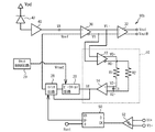
まず、PON用の光通信用増幅回路を用い、振幅の異なる信号を受信した場合正常に動作しない例を説明する。図1は、比較例に係る電子回路90(リミットアンプ)の回路図である。図1を参照に、PD42の出力電流を増幅したTIA40の出力電圧信号が入力信号VAとして電子回路90に入力される。電子回路90は差動増幅回路30、32及びフィードバック回路10を有している。差動増幅回路30は入力信号VAと参照信号Vrefとを差動増幅し、差動出力信号V1+及びV1−を出力する。差動増幅回路32は差動出力信号V1+及びV1−を増幅し、振幅を制限することでパルス信号である差動出力信号Vout及びVoutBを出力する。このように、差動増幅回路30及び32は、デジタル情報を含んだ高周波信号であるデジタル入力信号VAを参照信号Vrefと比較することで、パルス信号に変換するパルス変換回路である。
First, an example will be described in which a PON optical communication amplifier circuit is used and does not operate normally when signals having different amplitudes are received. FIG. 1 is a circuit diagram of an electronic circuit 90 (limit amplifier) according to a comparative example. Referring to FIG. 1, the output voltage signal of
フィードバック回路10には差動増幅回路30の差動出力信号V1+及びV1−が入力し、電子回路90の入力信号VAの平均値信号を出力する。フィードバック回路10は差動増幅回路12、14及び平滑回路16を有している。差動増幅回路12は、差動信号V1+及びV1−が入力し、差動増幅し、差動信号V0+及びV0−を出力する。差動信号V0+及びV0−は平滑回路16のそれぞれ抵抗R1及びR2を介し差動増幅回路14に差動信号V2+及びV2−として入力される。差動信号V2+及びV2−は平滑回路16のキャパシタC1により接続される。平滑回路16は抵抗R1、R2及びキャパシタC1により定まる時定数により、差動信号V1+及びV1−を平滑化し、差動信号V2+及びV2−とする。差動増幅回路14は差動信号V2+及びV2−を差動増幅し、参照信号Vrefとして差動増幅回路30に出力する。
The
フィードバック回路10においては、参照信号Vrefが平滑回路16の時定数相当で平滑化された入力信号VAに対して低いと、参照信号Vrefは大きくなる。一方、参照信号Vrefが平滑回路16の時定数相当で平滑化された入力信号VAに対して高いと、参照信号Vrefは小さくなる。このように、フィードバック回路10は、入力信号VAを平滑回路16の時定数で平均化した平均値信号を参照信号Vrefとして出力する。
In the
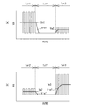
図2(a)は、PON方式のブロック図である。局舎60内の局側通信装置62は、複数の家庭70aから70c内の各家庭側通信装置72と光ファイバである通信経路L1及びL2を介し接続されている。局側通信装置62とオプティカルスプリッタ74とは1本の通信経路L1である。オプティカルスプリッタ74と各家庭側通信装置72との間は各通信経路L2を介し接続されている。オプティカルスプリッタ74は、各家庭側通信装置72から各通信経路L2を介し入出力された信号を通信経路L1に結合する。通信経路L1の信号は局側通信装置62に入出力される。局側通信装置62は制御回路64、送信部66及び受信部68を有している。送信部66は、各家庭側通信装置72に光信号を送信する送信回路である。受信部68は、各家庭側通信装置72からの光信号を受信する受信回路であり、図1に示した電子回路90を有している。制御回路64は送信部66及び受信部68を制御する回路であり、例えば、受信部68にリセット信号を出力する。
FIG. 2A is a block diagram of the PON system. The station
図2(b)は、受信部68のPD42に入力される光信号を時間に対し示す模式図である。期間Ton1の間は家庭70aの家庭側通信装置72からの光信号が入力される。期間Toff1の間は光信号は入力されず、期間Ton2において家庭70bの家庭側通信装置(不図示)からの光信号が入力される。さらに、期間Toff2の間は光信号は入力されず、期間Ton3において家庭70cの家庭側通信装置(不図示)からの光信号が入力される。各家庭側通信装置72の出力信号の振幅及び各通信経路L2での光信号の損失はそれぞれ異なる。このため、期間Ton1、Ton2及びTon3の光信号の振幅はそれぞれ振幅A1、A2及びA3と異なる。このように、PON用のPD42には、異なる家庭から光信号が異なる振幅で不定期に入力される。なお、期間Toff1及びToff2は通信経路L2を切り換える期間である。
FIG. 2B is a schematic diagram showing an optical signal input to the
図3(a)及び図3(b)は、時間に対する入力信号VAと参照信号Vrefとを示した図である。図3(a)及び図3(b)を参照に、期間Toffにおいて、PD42に光信号は入力されない。よって、入力信号VAは初期値である。期間Tonにおいて、PD42に光信号が入力され、入力信号VAが変動する。ある一定期間(プリアンブル期間Tpre)においては、オン、オフ信号(0、1信号)が交互に入力される。差動増幅回路30及び差動増幅回路32は、参照信号Vrefに対し入力信号VAに対し大きいか小さいかでハイレベルまたはローレベルを出力信号Vout及びVoutBとして出力する。このため、参照信号Vrefは早期に、入力信号VAの平均値Vmとなることが好ましい。しかしながら、図3(a)のように、平滑回路16の時定数が長いと、参照信号Vrefは早期には平均値Vmとはならない。このように、プリアンブル期間Tpre内に参照信号Vrefが安定化しない。一方、図3(b)のように、平滑回路16の時定数が短いと、参照信号Vrefはプリアンブル期間Tpre内に早期に平均値Vmとなるが、その後、入力信号VAの変動に同期し参照信号Vrefも変動してしまう。
FIGS. 3A and 3B are diagrams showing the input signal VA and the reference signal Vref with respect to time. Referring to FIGS. 3A and 3B, no optical signal is input to the
このように、比較例においては、参照信号Vrefを早期に平均値Vmに関係した信号とすることが難しい。よって、光信号のプリアンブル期間Tpreを短くすることができず、高速化の障害となる。このような課題を解決するための実施例を以下に説明する。 Thus, in the comparative example, it is difficult to make the reference signal Vref a signal related to the average value Vm at an early stage. Therefore, the preamble period Tpre of the optical signal cannot be shortened, which hinders speeding up. An embodiment for solving such a problem will be described below.
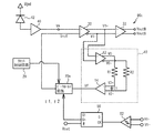
図4は実施例1に係る電子回路90aの回路図である。比較例1の図1と比較し、電子回路90aはピークホールド回路20(保持回路)を有している。ピークホールド回路20にはフィードバック回路10の出力信号Vfが入力し、参照信号Vrefが出力する。また、ピークホールド回路20のリセット端子にはリセット制御回路29からリセット信号Vrsetが入力される。その他の構成は比較例1の図1と同じであり説明を省略する。
FIG. 4 is a circuit diagram of the
図5はピークホールド回路20の回路図である。ピークホールド回路20は差動増幅回路22、24、ダイオードD1、キャパシタC2及びリセット回路25を有している。差動増幅回路22は、フィードバック回路10の出力信号Vfと参照信号Vrefとを差動増幅する。差動増幅回路22の出力はダイオードD1のアノードに接続する。ダイオードD1のカソードは差動増幅回路24の入力に接続される。差動増幅回路24は、信号Vpと参照信号Vrefとを差動増幅し参照信号Vrefを出力する。ダイオードD1のカソードとグランドとの間には、キャパシタC2とリセット回路25とが並列に接続される。リセット回路25はNPNバイポーラトランジスタ26である。トランジスタ26のコレクタがダイオードD1のカソードに、エミッタがグランドに接続され、ベースにリセット制御回路29からリセット信号Vrsetが入力される。
FIG. 5 is a circuit diagram of the
信号Vfが参照信号Vrefより大きいと、差動増幅回路22は正の信号を出力し、ダイオードD1を介しキャパシタC2を充電し、信号Vpの電位が定まる。差動増幅回路24は信号Vpと参照信号Vrefとを差動増幅する。よって、参照信号Vrefは信号Vpとなる。信号Vfが参照信号Vrefより小さいと、差動増幅回路22は負の信号を出力するが、ダイオードD1は逆方向のため、信号Vpは変化しない。以上により、ピークホールド回路20は、信号Vfの極大値に参照信号Vrefを保持する。
When the signal Vf is larger than the reference signal Vref, the
図6は入力信号VAと参照信号Vrefとを示した図である。図6を参照に、平滑回路16の時定数を図3(b)のように短くする。これにより、参照信号Vrefは入力信号VAに追従し早期に立ち上がる。入力信号VAがローレベルの場合も、ピークホールド回路20が参照信号Vrefのピークを保持するため、図3(b)のような参照信号Vrefの時間に対する変動は小さく、プリアンブル期間Tpre内に参照信号Vrefは早期に入力信号VAの平均値Vmに達し安定する。このように、実施例1の電子回路90aは、入力信号VAと参照信号Vrefとが入力する差動増幅回路30と、入力信号VAの平均値である信号Vfを出力するフィードバック回路10と、フィードバック回路10の出力信号Vfに基づいて保持された出力信号Vfの極大値を参照信号Vrefとして出力するピークホールド回路20と、を有している。これにより、早期に安定可能な参照信号Vrefを得ることができる。ピークホールド回路20の出力信号は、信号Vfの極大値に近い場合であってもよい。この場合も、図7において説明した効果を得ることができる。
FIG. 6 is a diagram showing the input signal VA and the reference signal Vref. Referring to FIG. 6, the time constant of the smoothing circuit 16 is shortened as shown in FIG. Thereby, the reference signal Vref follows the input signal VA and rises early. Even when the input signal VA is at a low level, the
また、ピークホールド回路20の極大値を保持する時定数は、フィードバック回路10の平均値を出力するための平滑回路16の時定数より大きいことが好ましい。これにより、参照信号Vrefが入力信号VAの変動に影響され変動することを抑制することができる。
The time constant for holding the maximum value of the
リセット回路25の機能について説明する。図7(a)及び図7(b)はトランジスタ26が常にオフ状態の場合の入力信号VAと参照信号Vrefとのタイミングチャートである。図7(a)は、振幅の大きい信号が入力される期間Ton1、信号が入力されない期間Toff、振幅の小さな信号が入力される期間Ton2を示している。トランジスタ26がオフ状態であると、ピークホールド回路20の極大値を保持する時定数が大きいため、期間Toffにおいても、ピークホールド回路20は参照信号Vrefとして、期間Ton1の平均値Vm1に近い値を保持してしまう。このため、期間Ton2において、振幅の小さい信号が入力された場合、図7(a)のAのように、参照信号Vrefが信号VAに対応することができない。
The function of the
図7(b)は、振幅の小さい信号が入力される期間Ton2、信号が入力されない期間Toff、振幅の大きな信号が入力される期間Ton3を示している。期間Toffの参照信号Vrefが期間Ton2の平均値Vm2に保持されていても、期間Ton3において、振幅の大きな信号VAが入力されるため、参照信号Vrefは入力信号VAに対応することができる。 FIG. 7B shows a period Ton2 in which a signal having a small amplitude is input, a period Toff in which no signal is input, and a period Ton3 in which a signal having a large amplitude is input. Even if the reference signal Vref in the period Toff is held at the average value Vm2 in the period Ton2, the signal VA having a large amplitude is input in the period Ton3. Therefore, the reference signal Vref can correspond to the input signal VA.
以上のように、トランジスタ26がオフ状態の場合、振幅の大きな入力信号の後に振幅の小さな信号が入力されると、参照信号Vrefが入力信号VAに対応できない。そこで、トランジスタ26を用い、参照信号Vrefを初期値に戻す。
As described above, when the
図8(a)及び図8(b)はトランジスタ26を用い参照信号Vrefをリセットする場合の入力信号VAと参照信号Vrefとのタイミングチャートである。期間Toffにおいて、トランジスタ26をオンし、参照信号Vrefを初期化する。これにより、図8(a)のように、期間Ton1において、振幅の大きな信号が入力された後、期間Ton2において、振幅の小さな信号が入力された場合も、参照信号Vrefは入力信号VAに対応することができる。また、例えば、PON方式用のリミットアンプには、シングルディテクト機能を有する場合がある。この機能は、入力信号が所定レベルを越えた場合または所定レベルを下回った場合、入力信号が途切れたとアラームを出す機能である。この機能を用いる場合、入力信号の振幅によらず、基準レベルを合わせるため、参照信号Vrefは期間Toffにおいて、初期値にすることが好ましい。よって、図8(b)のように、振幅の小さな入力信号VAの後、振幅の大きな入力信号NAが入力された場合も参照信号Vrefを初期値に戻すことが好ましい。
FIGS. 8A and 8B are timing charts of the input signal VA and the reference signal Vref when the
図9(a)から図9(c)は、実施例1に係る電子回路90aのシミュレーション結果である。図9(a)は時間に対する入力信号VA及び参照信号Vref、図9(b)はリセット信号Vrset、図9(c)は出力信号Vout及びVoutBを示している。期間Ton2は入力信号VAの振幅が小さく、期間Ton3は入力信号VAは大きい。期間Toffにおいて、リセット信号Vrsetにより、ピークホールド回路20を初期化している。入力信号VAが入力されると、参照信号Vrefは入力信号VAに追従し、早期に安定する。出力信号Vout及びVoutBは誤動作することなく正常な出力となる。
FIG. 9A to FIG. 9C are simulation results of the
このように、ピークホールド回路20は、参照信号Vrefを一定値に設定するリセット回路25を有することが好ましい。これにより、参照信号Vrefを図8(a)から図9(a)のように、リセットすることができるため、図7(a)で説明したように、期間Ton2において、参照信号Vrefが入力信号VAの平均値Vm2を上回ることがない。リセット回路25としてはFET等のトランジスタを用いることもできる。
Thus, the
トランジスタ26が設定する参照信号Vrefの一定値は、入力信号VAの初期値であることが好ましい。ここで、初期値とは、入力信号VAとして初期の直流電圧が入力された場合の参照信号Vrefである。例えば、図4において、PD42に光信号が入力されていないとき、TIA40が出力する電圧を入力信号VAとして無限時間経過の参照信号Vrefに相当する。実施例1では、初期値は入力信号VAのローレベルに相当する。
The constant value of the reference signal Vref set by the
(参考例)
参考例は、フィードバック回路の出力とピークホールド回路の出力とを切り換えるスイッチ回路を有する例である。図10は、参考例に係る電子回路の回路図である。図10を参照に、電子回路90bは、実施例1の図4の電子回路90aに加え、スイッチ回路28、カウンタ50及びヒステリシス比較器52を有している。
(Reference example)
The reference example is an example having a switch circuit that switches between the output of the feedback circuit and the output of the peak hold circuit. FIG. 10 is a circuit diagram of an electronic circuit according to a reference example . Referring to FIG. 10, an
差動増幅回路30の差動出力信号V1+及びV1−がヒステリシス比較器52に入力される。ヒステリシス比較器52は、差動信号V1+とV1−のノイズを除去し差動信号V+1とV1−との1周期毎にハイレベルのパルスをカウンタ50のクロックCKに入力する。これにより、カウンタ50はクロックのハイレベルのパルスの回数、すなわち差動信号V1+及びV1−の周期の回数毎にカウントする。カウントがnになると出力Qnがローレベルからハイレベルになる。カウンタ50の出力Qnはスイッチ回路28に入力される。スイッチ回路28は、出力Qnがローレベルのとき、フィードバック回路10の出力を参照信号Vrefとし、出力Qnがハイレベルのとき、ピークホールド回路20の出力を参照信号Vrefとする。すなわち、スイッチ回路28は入力信号VAが入力後、一定時間(V1+のハイレベルがn回まで)は、フィードバック回路10の出力を参照信号Vrefとし、一定時間経過時に、ピークホールド回路20の出力を参照信号Vrefに切り換える。期間Toffにおいて、リセットRにハイレベルを入力し、カウンタ50をリセットする。なお、リセットRに入力する信号は、リセット回路25に入力するリセット信号Vrsetを流用してもよい。
The differential output signals V1 + and V1- of the
図11(a)及び図11(b)は参考例に係る電子回路90bの効果を説明するための図である。図11(a)を参照に、実施例1に係る電子回路90aにおいて、入力信号VAが入力された際サージが入力されると、ピークホールド回路20はサージを極大値として認識しサージの値を保持してしまう。これにより、参照信号Vrefは平均値Vmに対し大きい状態となり、誤動作の原因となる。特に、入力信号VAが入力するとピークホールド回路20の帰還部等の影響によりサージが発生しやすい。
FIG. 11A and FIG. 11B are diagrams for explaining the effect of the
図11(b)を参照に、入力信号VAが入力後一定時間経過するまでの期間T1においては、フィードバック回路10の出力を参照信号Vrefとする。一定時間経過後の期間T2においては、ピークホールド回路20の出力を参照信号Vrefとする。これにより、サージの発生しやすい期間T1では、サージが発生しても参照信号Vrefは余りサージに影響されない。一方、サージの発生が起こりにくい期間T2においては、ピークホールド回路20の出力を参照信号Vrefとする。これにより、早期に参照信号Vrefを安定化することができる。
Referring to FIG. 11B, the output of the
参考例によれば、スイッチ回路28は、入力信号VAが入力された後一定時間後に、参照信号Vrefをフィードバック回路10の出力信号Vfからピークホールド回路20の出力に切り換える。これにより、入力信号VAが入力された初期のサージによる誤動作を抑制することができる。
According to the reference example , the
実施例2はピークホールド回路の時定数を切り換える例である。図12は実施例2に係る電子回路90cの回路図である。図12を参照に、実施例2に係る電子回路90cは実施例1の図4に比較し、ピークホールド回路20aに、参考例の図10に示したカウンタ50の出力Qnが入力される。その他の構成は実施例1と同じであり説明を省略する。
The second embodiment is an example in which the time constant of the peak hold circuit is switched. FIG. 12 is a circuit diagram of an
ピークホールド回路20aは、出力Qnがローレベルのときは、極大値を保持する時定数を小さな値τ1とし、出力Qnがハイレベルのときは、時定数を大きな値τ2とする。実施例2のように、入力信号VAが入力されてから一定時間後に、ピークホールド回路20aは、極大値を保持する時定数を小さな時定数τ1から大きな時定数τ2に切り換える。これにより、参考例と同様に、入力信号VAが入力された初期に発生したサージに起因し、電子回路90cが誤動作することを抑制することができる。
The
実施例1から実施例2において、入力信号VAとしてTIA40の出力信号である場合を例に説明した。しかしながら、入力信号VAはTIAの出力信号以外の場合でもよい。また、PON方式の光通信に用いる増幅回路の場合、特に、振幅の異なる信号が入力されるため実施例1から実施例2の電子回路を用いることが好ましい。
In the first to second embodiments, the case where the input signal VA is the output signal of the
実施例1から実施例2においては、ピークホールド回路20、20aとしてフィードバック回路10の出力の極大値を保持する回路を例に説明した。ピークホールド回路20、20aはフィードバック回路10の出力は極大値に限られない。上記効果を奏するためには、極大値に近いことが好ましい。さらに、ピークホールド回路20、20aはフィードバック回路10の出力の極小値または極小値に近い値を保持してもよい。このように、ピークホールド回路20の出力信号は、フィードバック回路10の出力信号Vfに基づいて保持された信号であればよい。
In the first embodiment to the second embodiment , the
実施例3は実施例1に係る電子回路90aを、図2(a)に係るPON方式の局側通信装置62の受信部68に用いた通信システムの例である。つまり、局側通信装置62は、複数の通信経路L2に対し通信を行う通信システムである。図2(a)及び図4を参照に、局側通信装置62は、差動増幅回路30及び32(パルス変換回路)、フィードバック回路10(平均値生成回路)ピークホールド回路20(保持回路)と、を有している。差動増幅回路30及び32は、複数の通信経路L2のうち1つの通信経路L2から入力された光信号をPD42及びTIA40を用い電気信号に変換された入力信号VAを参照信号Vref(基準値)と比較することでパルス列に変換する回路である。フィードバック回路10(平均値生成回路)は、差動増幅回路30の入力信号VA(パルス変換回路の入力)に基づいて、入力信号VAの振幅の平均値を生成する回路である。ピークホールド回路20は、フィードバック回路10の出力信号Vfに基づいて保持された信号(信号Vfの極大値)を参照信号Vrefとして出力する回路である。家庭から送信される光信号にはリセット信号は含まれていない。すなわち、入力信号VAにはリセット信号は含まれていない。このため、リセット信号Vrsetを制御するリセット制御回路29は局側通信装置62の制御回路64の信号によって制御される。
The third embodiment is an example of a communication system in which the
実施例3によれば、図8(a)及び図8(b)のように、ピークホールド回路20は、1つの通信経路L2(例えば家庭70aと接続する通信経路L2)を複数の通信経路L2のうち別の通信経路L2(例えば家庭70bと接続する通信経路L2)に切り換える期間Toffに生成されるリセット信号Vrsetに基づき、ピークホールド回路20の出力信号を所定の値(実施例ではグランド)にリセットする。このような通信システムにより、図2(b)のように複数の通信経路L2から受信した振幅の異なる光信号であっても、参照信号Vrefを早期に安定させるとともに参照信号Vrefを一定の値に設定することができる。これにより、プリアンブル期間Tpreを短くすることができる。よって、通信を高速で行うことができる。実施例3は、実施例1を適用した通信システムの例であったが実施例2を適用することもできる。
According to the third embodiment , as shown in FIGS. 8A and 8B, the
以上、本発明の実施例について詳述したが、本発明は係る特定の実施例に限定されるものではなく、特許請求の範囲に記載された本発明の要旨の範囲内において、種々の変形・変更が可能である。 Although the embodiments of the present invention have been described in detail above, the present invention is not limited to such specific embodiments, and various modifications and changes can be made within the scope of the gist of the present invention described in the claims. It can be changed.
10 フィードバック回路
12、14 差動増幅回路
16 平滑回路
20 ピークホールド回路
22、24 差動増幅回路
25 リセット回路
30、32 差動増幅回路
40 TIA
42 フォトダイオード
50 カウンタ
52 ヒステリシス比較器
DESCRIPTION OF
42
Claims (6)
前記差動増幅回路から出力される2つの差動信号の振幅の平均値を出力するための平滑回路を備えるフィードバック回路と、
前記フィードバック回路の出力信号に基づいてピークホールドされた信号を前記参照信号として出力するピークホールド回路と、を具備し、
前記ピークホールド回路の極大値を保持する時定数は、前記平滑回路の時定数より大きいことを特徴とする電子回路。 A differential amplifier circuit to which a digital input signal and a reference signal are input;
A feedback circuit including a smoothing circuit for outputting an average value of amplitudes of two differential signals output from the differential amplifier circuit ;
Anda peak hold circuit for outputting a signal peak hold as the reference signal based on an output signal of said feedback circuit,
An electronic circuit characterized in that the time constant for holding the maximum value of the peak hold circuit is larger than the time constant of the smoothing circuit.
前記ピークホールド回路の保持された信号を保持する時定数は、前記プリアンブル期間の周期より長いことを特徴とする請求項1から3のいずれか一項記載の電子回路。 The peak hold circuit holds a maximum value of the output signal of the feedback circuit with a time constant shorter than a period of a preamble period of the input signal;
4. The electronic circuit according to claim 1, wherein a time constant for holding the signal held by the peak hold circuit is longer than a period of the preamble period.
前記入力信号は、振幅の大きさが異なるデジタル信号であることを特徴とする請求項1記載の電子回路。 The electronic circuit is a receiving circuit for optical communication,
2. The electronic circuit according to claim 1, wherein the input signals are digital signals having different amplitudes.
Priority Applications (3)
| Application Number | Priority Date | Filing Date | Title |
|---|---|---|---|
| JP2007044468A JP5101131B2 (en) | 2007-02-23 | 2007-02-23 | Electronic circuit |
| PCT/JP2008/052889 WO2008102819A1 (en) | 2007-02-23 | 2008-02-20 | Electronic circuit and communication system |
| US12/546,192 US8301038B2 (en) | 2007-02-23 | 2009-08-24 | Electronic circuit and communication system |
Applications Claiming Priority (1)
| Application Number | Priority Date | Filing Date | Title |
|---|---|---|---|
| JP2007044468A JP5101131B2 (en) | 2007-02-23 | 2007-02-23 | Electronic circuit |
Publications (3)
| Publication Number | Publication Date |
|---|---|
| JP2008211376A JP2008211376A (en) | 2008-09-11 |
| JP2008211376A5 JP2008211376A5 (en) | 2008-11-20 |
| JP5101131B2 true JP5101131B2 (en) | 2012-12-19 |
Family
ID=39710093
Family Applications (1)
| Application Number | Title | Priority Date | Filing Date |
|---|---|---|---|
| JP2007044468A Active JP5101131B2 (en) | 2007-02-23 | 2007-02-23 | Electronic circuit |
Country Status (3)
| Country | Link |
|---|---|
| US (1) | US8301038B2 (en) |
| JP (1) | JP5101131B2 (en) |
| WO (1) | WO2008102819A1 (en) |
Families Citing this family (5)
| Publication number | Priority date | Publication date | Assignee | Title |
|---|---|---|---|---|
| JP5215087B2 (en) * | 2008-08-29 | 2013-06-19 | 住友電工デバイス・イノベーション株式会社 | Electronic circuit |
| US8155536B2 (en) * | 2008-12-31 | 2012-04-10 | Intel Corporation | Optical transceiver IC |
| JP5280256B2 (en) * | 2009-03-12 | 2013-09-04 | 住友電工デバイス・イノベーション株式会社 | Electronic circuit |
| CN103477575A (en) * | 2011-04-20 | 2013-12-25 | 富士通光器件株式会社 | Detection device, light receiving device, detection method, and light receiving method |
| EP3208939B1 (en) | 2014-10-15 | 2018-09-26 | Fujikura Ltd. | Optical receiver, active optical cable, and control method for optical receiver |
Family Cites Families (15)
| Publication number | Priority date | Publication date | Assignee | Title |
|---|---|---|---|---|
| JPS6215909A (en) * | 1985-07-15 | 1987-01-24 | Hitachi Ltd | Optical reception circuit |
| JPS6374304A (en) * | 1986-09-18 | 1988-04-04 | Furukawa Electric Co Ltd:The | Compensating method for offset or drift or the like in optical receiving circuit |
| JPH0743807Y2 (en) * | 1988-10-11 | 1995-10-09 | ローム株式会社 | Tape player |
| JP3275212B2 (en) * | 1992-07-03 | 2002-04-15 | 富士通株式会社 | Optical signal demodulation method |
| JP3284506B2 (en) * | 1993-04-20 | 2002-05-20 | 日本電信電話株式会社 | Amplifier circuit |
| JPH08102716A (en) * | 1994-09-30 | 1996-04-16 | Hitachi Ltd | Burst optical reception circuit |
| JP2616480B2 (en) * | 1995-03-17 | 1997-06-04 | 日本電気株式会社 | Burst light receiving circuit |
| JP2814990B2 (en) * | 1996-05-20 | 1998-10-27 | 日本電気株式会社 | Optical receiving circuit |
| JP3085275B2 (en) * | 1998-02-18 | 2000-09-04 | 日本電気株式会社 | Binary optical transmission method and binary optical transmission system |
| JP3031326B2 (en) * | 1998-02-19 | 2000-04-10 | 日本電気株式会社 | Burst receiving circuit and method of controlling burst receiving circuit |
| US6084478A (en) * | 1998-08-20 | 2000-07-04 | Vitesse Semiconductor Corp. | Transimpedance amplifier with automatic gain control |
| JP4045223B2 (en) * | 2003-09-09 | 2008-02-13 | 株式会社日立製作所 | Burst optical receiver using gain switching method |
| JP2005123350A (en) * | 2003-10-16 | 2005-05-12 | Matsushita Electric Ind Co Ltd | Average power detecting circuit, laser diode driving circuit and light transmitting module |
| JP4613495B2 (en) | 2004-02-05 | 2011-01-19 | 住友電気工業株式会社 | Preamplifier |
| EP2003486A4 (en) * | 2006-03-31 | 2010-11-24 | Fujitsu Ltd | Differential four-phase shift modulator and method for controlling phase shift amount thereof |
-
2007
- 2007-02-23 JP JP2007044468A patent/JP5101131B2/en active Active
-
2008
- 2008-02-20 WO PCT/JP2008/052889 patent/WO2008102819A1/en active Application Filing
-
2009
- 2009-08-24 US US12/546,192 patent/US8301038B2/en active Active
Also Published As
| Publication number | Publication date |
|---|---|
| US20090310979A1 (en) | 2009-12-17 |
| WO2008102819A1 (en) | 2008-08-28 |
| US8301038B2 (en) | 2012-10-30 |
| JP2008211376A (en) | 2008-09-11 |
Similar Documents
| Publication | Publication Date | Title |
|---|---|---|
| JP4850919B2 (en) | Optical receiver | |
| JP4870806B2 (en) | Transimpedance amplifier | |
| US7583904B2 (en) | Transimpedance (TIA) circuit usable for burst mode communications | |
| JP5280256B2 (en) | Electronic circuit | |
| US9673797B2 (en) | Peak detector using charge pump and burst-mode transimpedance amplifier | |
| WO2011099598A1 (en) | Optical signal turn-off detection circuit and optical receiver | |
| WO2016035176A1 (en) | Optical receiver, optical terminal apparatus, and optical communication system | |
| JP4833124B2 (en) | Transimpedance amplifier and control method of transimpedance amplifier | |
| JP5725168B2 (en) | Detection device, optical receiver, detection method, and optical reception method | |
| KR100630089B1 (en) | Burst-mode optical receiver of differential output structure | |
| JP5101131B2 (en) | Electronic circuit | |
| CN106851443B (en) | OLT (optical line terminal) transceiver integrated chip | |
| US9496826B2 (en) | Transimpedance amplifier | |
| JP5864025B2 (en) | Burst optical receiver and bias voltage control method for APD of burst optical receiver | |
| JP5494285B2 (en) | Electronic circuit | |
| JP2009017265A (en) | Electronic circuit | |
| WO2013035139A1 (en) | Optical line terminal | |
| KR101519443B1 (en) | Optical receiver | |
| US7266312B2 (en) | Burst mode optical receiver | |
| JP2007274032A (en) | Optical receiver | |
| CN114389550A (en) | Transimpedance amplification circuit for receiving burst optical signal | |
| JP6661057B1 (en) | Limiting amplifier circuit | |
| US7206521B2 (en) | Signal level detecting device for a burst-mode optical receiver | |
| US7539424B2 (en) | Burst mode optical receiver for maintaining constant signal amplitude | |
| US20120032740A1 (en) | Amplifier for receiving intermittent optical signal |
Legal Events
| Date | Code | Title | Description |
|---|---|---|---|
| A521 | Request for written amendment filed |
Free format text: JAPANESE INTERMEDIATE CODE: A523 Effective date: 20081001 |
|
| A621 | Written request for application examination |
Free format text: JAPANESE INTERMEDIATE CODE: A621 Effective date: 20081001 |
|
| A131 | Notification of reasons for refusal |
Free format text: JAPANESE INTERMEDIATE CODE: A131 Effective date: 20110830 |
|
| A521 | Request for written amendment filed |
Free format text: JAPANESE INTERMEDIATE CODE: A523 Effective date: 20111021 |
|
| A131 | Notification of reasons for refusal |
Free format text: JAPANESE INTERMEDIATE CODE: A131 Effective date: 20120703 |
|
| A521 | Request for written amendment filed |
Free format text: JAPANESE INTERMEDIATE CODE: A523 Effective date: 20120903 |
|
| TRDD | Decision of grant or rejection written | ||
| A01 | Written decision to grant a patent or to grant a registration (utility model) |
Free format text: JAPANESE INTERMEDIATE CODE: A01 Effective date: 20120925 |
|
| A01 | Written decision to grant a patent or to grant a registration (utility model) |
Free format text: JAPANESE INTERMEDIATE CODE: A01 |
|
| A61 | First payment of annual fees (during grant procedure) |
Free format text: JAPANESE INTERMEDIATE CODE: A61 Effective date: 20120926 |
|
| FPAY | Renewal fee payment (event date is renewal date of database) |
Free format text: PAYMENT UNTIL: 20151005 Year of fee payment: 3 |
|
| R150 | Certificate of patent or registration of utility model |
Ref document number: 5101131 Country of ref document: JP Free format text: JAPANESE INTERMEDIATE CODE: R150 Free format text: JAPANESE INTERMEDIATE CODE: R150 |
|
| R250 | Receipt of annual fees |
Free format text: JAPANESE INTERMEDIATE CODE: R250 |
|
| R250 | Receipt of annual fees |
Free format text: JAPANESE INTERMEDIATE CODE: R250 |