JP5091028B2 - Switching regulator and semiconductor device including the switching regulator - Google Patents
Switching regulator and semiconductor device including the switching regulator Download PDFInfo
- Publication number
- JP5091028B2 JP5091028B2 JP2008167147A JP2008167147A JP5091028B2 JP 5091028 B2 JP5091028 B2 JP 5091028B2 JP 2008167147 A JP2008167147 A JP 2008167147A JP 2008167147 A JP2008167147 A JP 2008167147A JP 5091028 B2 JP5091028 B2 JP 5091028B2
- Authority
- JP
- Japan
- Prior art keywords
- signal
- circuit unit
- output
- control
- current
- Prior art date
- Legal status (The legal status is an assumption and is not a legal conclusion. Google has not performed a legal analysis and makes no representation as to the accuracy of the status listed.)
- Expired - Fee Related
Links
Images


Classifications
-
- H—ELECTRICITY
- H02—GENERATION; CONVERSION OR DISTRIBUTION OF ELECTRIC POWER
- H02M—APPARATUS FOR CONVERSION BETWEEN AC AND AC, BETWEEN AC AND DC, OR BETWEEN DC AND DC, AND FOR USE WITH MAINS OR SIMILAR POWER SUPPLY SYSTEMS; CONVERSION OF DC OR AC INPUT POWER INTO SURGE OUTPUT POWER; CONTROL OR REGULATION THEREOF
- H02M3/00—Conversion of dc power input into dc power output
- H02M3/02—Conversion of dc power input into dc power output without intermediate conversion into ac
- H02M3/04—Conversion of dc power input into dc power output without intermediate conversion into ac by static converters
- H02M3/10—Conversion of dc power input into dc power output without intermediate conversion into ac by static converters using discharge tubes with control electrode or semiconductor devices with control electrode
- H02M3/145—Conversion of dc power input into dc power output without intermediate conversion into ac by static converters using discharge tubes with control electrode or semiconductor devices with control electrode using devices of a triode or transistor type requiring continuous application of a control signal
- H02M3/155—Conversion of dc power input into dc power output without intermediate conversion into ac by static converters using discharge tubes with control electrode or semiconductor devices with control electrode using devices of a triode or transistor type requiring continuous application of a control signal using semiconductor devices only
- H02M3/156—Conversion of dc power input into dc power output without intermediate conversion into ac by static converters using discharge tubes with control electrode or semiconductor devices with control electrode using devices of a triode or transistor type requiring continuous application of a control signal using semiconductor devices only with automatic control of output voltage or current, e.g. switching regulators
- H02M3/158—Conversion of dc power input into dc power output without intermediate conversion into ac by static converters using discharge tubes with control electrode or semiconductor devices with control electrode using devices of a triode or transistor type requiring continuous application of a control signal using semiconductor devices only with automatic control of output voltage or current, e.g. switching regulators including plural semiconductor devices as final control devices for a single load
- H02M3/1588—Conversion of dc power input into dc power output without intermediate conversion into ac by static converters using discharge tubes with control electrode or semiconductor devices with control electrode using devices of a triode or transistor type requiring continuous application of a control signal using semiconductor devices only with automatic control of output voltage or current, e.g. switching regulators including plural semiconductor devices as final control devices for a single load comprising at least one synchronous rectifier element
-
- Y—GENERAL TAGGING OF NEW TECHNOLOGICAL DEVELOPMENTS; GENERAL TAGGING OF CROSS-SECTIONAL TECHNOLOGIES SPANNING OVER SEVERAL SECTIONS OF THE IPC; TECHNICAL SUBJECTS COVERED BY FORMER USPC CROSS-REFERENCE ART COLLECTIONS [XRACs] AND DIGESTS
- Y02—TECHNOLOGIES OR APPLICATIONS FOR MITIGATION OR ADAPTATION AGAINST CLIMATE CHANGE
- Y02B—CLIMATE CHANGE MITIGATION TECHNOLOGIES RELATED TO BUILDINGS, e.g. HOUSING, HOUSE APPLIANCES OR RELATED END-USER APPLICATIONS
- Y02B70/00—Technologies for an efficient end-user side electric power management and consumption
- Y02B70/10—Technologies improving the efficiency by using switched-mode power supplies [SMPS], i.e. efficient power electronics conversion e.g. power factor correction or reduction of losses in power supplies or efficient standby modes
Description
本発明は、スイッチングレギュレータに関し、特にPWM制御とVFM制御を、負荷の状態に応じて切り換えて行うようにしたスイッチングレギュレータに関する。 The present invention relates to a switching regulator, and more particularly to a switching regulator in which PWM control and VFM control are switched according to a load state.
近年、環境問題に対する配慮から、電子機器の省電力化が求められており、特に電池駆動による電子機器においてその傾向が顕著である。一般に省電力化を図るためには、電子機器で消費する電力を削減することと、電源回路自体の効率を向上させ無駄な電力消費を抑えることが重要であった。小型の電子機器に使用される高効率の電源回路方式としては、インダクタを使用した非絶縁型のスイッチングレギュレータが広く使用されている。
スイッチングレギュレータの制御方式には、大きく2つの方式が知られている。1つは、一定周波数のクロックパルスのデューティサイクルを変化させて出力電圧が一定になるように制御するPWM(pulse width modulation)制御であり、もう1つは、出力電圧の誤差に応じて、パルス幅が一定のクロック信号の出力を制御して、出力電圧が一定になるように制御するVFM(variable frequency modulation)制御である。
In recent years, in consideration of environmental problems, power saving of electronic devices has been demanded, and this tendency is particularly noticeable in battery-driven electronic devices. In general, in order to save power, it has been important to reduce the power consumed by the electronic device and to improve the efficiency of the power supply circuit itself to suppress wasteful power consumption. Non-insulated switching regulators using inductors are widely used as highly efficient power supply circuit systems used in small electronic devices.
There are two known control systems for switching regulators. One is PWM (pulse width modulation) control that controls the output voltage to be constant by changing the duty cycle of a clock pulse having a constant frequency, and the other is a pulse according to an error in the output voltage. This is VFM (variable frequency modulation) control for controlling the output of a clock signal having a constant width so that the output voltage becomes constant.
PWM制御は、軽負荷でも一定周期でスイチングトランジスタのオン/オフ制御を行うため、軽負荷での効率は悪化する。これに対して、VFM制御は、負荷に応じて周波数が変動するため、機器に対してノイズやリプルの影響が大きいが、軽負荷に対してはPWM制御よりも効率が高い。このようなことから、従来は、負荷の状態に応じて、PWM制御とVFM制御を切り換えて行うようにし、軽負荷から重負荷まで電源効率を高めていた。
負荷の状態を検出する方法は、入力電圧から出力端子の間における電流が流れる経路に出力電流検出用抵抗を挿入して出力電流を検出する方法が一般的であった。しかし、このような方法では、出力電流が大きくなるほど出力電流検出用抵抗による電力損失が増えるため、電池を電源にした小型電子機器には適さなかった。また、出力電流検出用抵抗を使用しない方法としては、誤差増幅回路の電圧レベルを使用して間接的に負荷の状態を検出するものがあった(例えば、特許文献1参照。)。
As a method for detecting the state of the load, a method of detecting an output current by inserting an output current detection resistor in a path through which a current flows between the input voltage and the output terminal has been common. However, such a method is not suitable for a small electronic device using a battery as a power source because the power loss due to the output current detection resistor increases as the output current increases. Further, as a method not using the output current detection resistor, there is a method of indirectly detecting the load state using the voltage level of the error amplifier circuit (see, for example, Patent Document 1).
しかし、前記誤差増幅回路は、出力電圧に重畳されているリップル成分の影響を除去するための積分回路を備えており、該積分回路は、通常、位相補償回路として設けられている。このような積分回路は、通常PWM制御時の動作周波数に合わせて最適化されているため、VFM制御時のようにPWM制御時よりも動作周波数が低くなったり、PWM制御に使用するパルス信号のパルスを間引きしたりすると、前記積分回路の出力信号は、前記誤差増幅回路の出力信号でもあることから、スイッチング動作直後は有効に機能するが、間引きを行う等してスイッチング動作が停止した状態では、接地電圧又は電源電圧の状態となり負荷電流を検出する信号としては有効に機能しなくなる。このため、VFM制御時は、前記誤差増幅回路の出力電圧が負荷電流に対して一定の電圧を維持することができなくなり、誤差増幅回路の出力電圧と負荷電流との関係は一定でなくなる。このようなことから、出力電流検出用抵抗を使用して負荷電流を測定して切り換える方式と比較して、制御の切り換え時における負荷電流を正確に設定することができないという問題があった。 However, the error amplifying circuit includes an integrating circuit for removing the influence of the ripple component superimposed on the output voltage, and the integrating circuit is usually provided as a phase compensation circuit. Since such an integration circuit is optimized in accordance with the operating frequency at the time of normal PWM control, the operating frequency is lower than at the time of PWM control as in the case of VFM control, or the pulse signal used for PWM control. When the pulse is thinned out, the output signal of the integration circuit is also the output signal of the error amplification circuit, so it functions effectively immediately after the switching operation, but in a state where the switching operation is stopped by thinning out or the like. Then, the ground voltage or the power supply voltage is entered, and the signal for detecting the load current does not function effectively. For this reason, during VFM control, the output voltage of the error amplifier circuit cannot maintain a constant voltage with respect to the load current, and the relationship between the output voltage of the error amplifier circuit and the load current is not constant. For this reason, there is a problem that the load current at the time of switching the control cannot be set accurately as compared with the method of measuring and switching the load current using the output current detection resistor.
本発明は、このような問題を解決するためになされたものであり、出力電流検出用抵抗を使用することなく、PWM制御とVFM制御の切り換わり時における負荷電流値を正確に設定することができるスイッチングレギュレータ及びそのスイッチングレギュレータを備えた半導体装置を得ることを目的とする。 The present invention has been made to solve such a problem, and can accurately set a load current value at the time of switching between PWM control and VFM control without using an output current detection resistor. An object of the present invention is to obtain a switching regulator that can be used and a semiconductor device including the switching regulator.
この発明に係るスイッチングレギュレータは、PWM制御とVFM制御を自動的に切り換えて行い、入力端子に入力された入力電圧を、所定の定電圧に変換して出力端子から出力電圧として出力するスイッチングレギュレータにおいて、
入力された制御信号に応じてスイッチングを行うスイッチ素子と、
該スイッチ素子のスイッチングによって前記入力電圧による充電が行われるインダクタと、
前記スイッチ素子がオフして該インダクタへの充電が停止すると、該インダクタの放電を行う整流素子と、
前記出力電圧に比例した比例電圧と所定の第1基準電圧との電圧比較を行い、該比較結果を示す信号を出力すると共に該各電圧の電圧差を増幅して誤差電圧を生成し出力する誤差増幅回路部と、
前記誤差電圧をPWM変調して、前記PWM制御を行うためのPWMパルス信号を生成し出力するPWMパルス生成回路部と、
前記スイッチ素子を流れる電流であるハイサイド電流と、前記整流素子を流れる電流であるローサイド電流の検出を行い、該検出結果を示す信号を生成して出力する電流検出回路部と、
前記出力電圧の検出を行い、該出力電圧が所定値以下に低下したことを検出すると所定の信号を出力する出力電圧低下検出回路部と、
前記PWMパルス信号における前記スイッチ素子をオンさせるタイミングを示したエッジと、前記電流検出回路部の出力信号におけるハイサイド電流が所定値になったことを示すエッジとの間隔のパルス幅を有する電流パルス信号を生成して出力する電流パルス生成回路部と、
前記PWMパルス信号と該電流パルス信号との各位相を比較し、該比較結果を示す信号を生成して出力する位相検出回路部と、
前記電流検出回路部の出力信号から、VFM制御を行うためのVFMパルス信号を生成して出力するVFMパルス生成回路部と、
前記PWMパルス信号を使用したPWM制御又は該VFMパルス信号を使用したVFM制御のいずれかの制御で前記スイッチ素子のスイッチング制御を行うスイッチング制御回路部と、
を備え、
前記スイッチング制御回路部は、前記位相検出回路部の出力信号に応じてPWM制御からVFM制御への切り換えを行い、前記出力電圧低下検出回路部の出力信号に応じてVFM制御からPWM制御への切り換えを行うものである。
The switching regulator according to the present invention is a switching regulator that automatically switches between PWM control and VFM control, converts an input voltage input to an input terminal into a predetermined constant voltage, and outputs the voltage as an output voltage from the output terminal. ,
A switching element that performs switching according to the input control signal;
An inductor that is charged by the input voltage by switching of the switch element;
When the switching element is turned off and charging to the inductor is stopped, the rectifying element that discharges the inductor;
An error in which a proportional voltage proportional to the output voltage is compared with a predetermined first reference voltage, a signal indicating the comparison result is output, and an error voltage is generated by amplifying the voltage difference between the voltages. An amplification circuit section;
A PWM pulse generation circuit unit that PWM-modulates the error voltage and generates and outputs a PWM pulse signal for performing the PWM control;
A current detection circuit unit that detects a high-side current that flows through the switch element and a low-side current that flows through the rectifier element, generates a signal indicating the detection result, and outputs the signal;
An output voltage drop detection circuit unit that detects the output voltage and outputs a predetermined signal when detecting that the output voltage has decreased below a predetermined value;
A current pulse having a pulse width of an interval between an edge indicating the timing for turning on the switch element in the PWM pulse signal and an edge indicating that the high-side current in the output signal of the current detection circuit unit has reached a predetermined value. A current pulse generation circuit for generating and outputting a signal;
A phase detection circuit unit for comparing each phase of the PWM pulse signal and the current pulse signal, and generating and outputting a signal indicating the comparison result;
A VFM pulse generation circuit unit that generates and outputs a VFM pulse signal for performing VFM control from an output signal of the current detection circuit unit;
A switching control circuit unit that performs switching control of the switch element by either PWM control using the PWM pulse signal or VFM control using the VFM pulse signal;
With
The switching control circuit unit switches from PWM control to VFM control according to the output signal of the phase detection circuit unit, and switches from VFM control to PWM control according to the output signal of the output voltage drop detection circuit unit. Is to do.
具体的には、前記スイッチング制御回路部は、前記位相検出回路部から、前記PWMパルス信号と前記電流パルス信号の位相が一致したことを示す信号が入力されると前記PWM制御から前記VFM制御への切り換えを行い、前記出力電圧低下検出回路部から前記所定の信号が入力されると前記VFM制御から前記PWM制御への切り換えを行うようにした。 Specifically, the switching control circuit unit changes from the PWM control to the VFM control when a signal indicating that the phases of the PWM pulse signal and the current pulse signal coincide with each other is input from the phase detection circuit unit. When the predetermined signal is input from the output voltage drop detection circuit unit, switching from the VFM control to the PWM control is performed.
また、前記電流検出回路部は、前記スイッチング制御回路部がPWM制御を行う場合、前記ハイサイド電流が所定の第1電流値以上であることを検出すると所定の第1信号を出力するようにした。 Further, when the switching control circuit unit performs PWM control, the current detection circuit unit outputs a predetermined first signal when detecting that the high-side current is equal to or higher than a predetermined first current value. .
また、前記電流検出回路部は、前記スイッチング制御回路部がVFM制御を行う場合は、前記ハイサイド電流が所定の第2電流値以上であることを検出すると前記所定の第1信号を出力し、前記ローサイド電流が前記第2電流値よりも小さい所定の第3電流値以下であることを検出すると所定の第2信号を出力するようにした。 Further, when the switching control circuit unit performs VFM control, the current detection circuit unit outputs the predetermined first signal when detecting that the high-side current is equal to or higher than a predetermined second current value, When it is detected that the low-side current is equal to or smaller than a predetermined third current value smaller than the second current value, a predetermined second signal is output.
また、前記VFMパルス生成回路部は、前記誤差増幅回路部から前記比例電圧が前記第1基準電圧以下になったことを示す信号が出力されている間に、前記所定の第2信号が前記電流検出回路部から出力された時点と、前記所定の第1信号が前記電流検出回路部から出力された時点との間、前記スイッチ素子をオンさせて導通状態にするように、前記VFMパルス信号を生成するようにした。 The VFM pulse generation circuit unit outputs the predetermined second signal while the signal indicating that the proportional voltage has become equal to or lower than the first reference voltage is output from the error amplification circuit unit. The VFM pulse signal is turned on so that the switch element is turned on to be in a conductive state between the time when it is output from the detection circuit unit and the time when the predetermined first signal is output from the current detection circuit unit. Generated.
また、前記VFMパルス生成回路部は、前記誤差増幅回路部から前記比例電圧が前記第1基準電圧以下になったことを示す信号が出力されたときに、前記所定の第2信号が前記電流検出回路部から出力されていない場合、前記誤差増幅回路部から前記比例電圧が前記第1基準電圧以下になったことを示す信号が出力された時点と、前記所定の第1信号が前記電流検出回路部から出力された時点との間、前記スイッチ素子をオンさせて導通状態にするように、前記VFMパルス信号を生成するようにした。 The VFM pulse generation circuit unit outputs the current detection signal when the signal indicating that the proportional voltage has become equal to or lower than the first reference voltage is output from the error amplification circuit unit. When the signal is not output from the circuit unit, when the signal indicating that the proportional voltage is equal to or lower than the first reference voltage is output from the error amplification circuit unit, and the predetermined first signal is the current detection circuit The VFM pulse signal is generated so that the switch element is turned on to be in a conductive state between the time when the signal is output from the unit.
また、前記電流パルス生成回路部は、前記スイッチング制御回路部が前記スイッチ素子をオンさせて導通状態にした時点から、前記電流検出回路部から前記所定の第1信号が出力された時点又は前記スイッチング制御回路部が前記スイッチ素子をオフさせて遮断状態にした時点のいずれか早い方の時点までの間のパルス幅を有する前記電流パルス信号を生成するようにした。 In addition, the current pulse generation circuit unit may be configured such that when the predetermined first signal is output from the current detection circuit unit from when the switching control circuit unit turns on the switch element to be in a conductive state, or when the switching is performed. The current pulse signal having a pulse width between the time point when the control circuit unit turns off the switch element and puts it into the cut-off state, whichever is earlier, is generated.
また、この発明に係る半導体装置は、前記スイッチングレギュレータのいずれかを備えるようにした。 The semiconductor device according to the present invention includes any one of the switching regulators.
本発明のスイッチングレギュレータ及びそのスイッチングレギュレータを備えた半導体装置によれば、前記スイッチング制御回路部が、前記位相検出回路部の出力信号に応じてPWM制御からVFM制御への切り換えを行い、前記出力電圧低下検出回路部の出力信号に応じてVFM制御からPWM制御への切り換えを行うようにした。具体的には、PWM制御とVFM制御との切り換え時における負荷電流が、PWM制御からVFM制御への移行時は、前記第1電流値で決まる負荷電流で切り換わり、VFM制御からPWM制御への移行時は、前記第2電流値及び第3電流値で決まる負荷電流で切り換えるようにした。このことから、出力電流検出用抵抗を使用することなく、PWM制御とVFM制御の切り換わり時における負荷電流値を正確に設定することができる。 According to the switching regulator and the semiconductor device including the switching regulator of the present invention, the switching control circuit unit switches from PWM control to VFM control according to the output signal of the phase detection circuit unit, and the output voltage Switching from VFM control to PWM control is performed in accordance with the output signal of the drop detection circuit unit. Specifically, the load current at the time of switching between PWM control and VFM control is switched at the load current determined by the first current value when shifting from PWM control to VFM control, and from VFM control to PWM control. At the time of transition, switching is performed with a load current determined by the second current value and the third current value. Thus, the load current value at the time of switching between PWM control and VFM control can be accurately set without using an output current detection resistor.
次に、図面に示す実施の形態に基づいて、本発明を詳細に説明する。
第1の実施の形態.
図1は、本発明の第1の実施の形態におけるスイッチングレギュレータの回路例を示した図である。
図1のスイッチングレギュレータ1は、入力端子INに入力された入力電圧Vinを所定の定電圧に降圧して出力電圧Voutとして出力端子OUTから出力する同期整流方式の降圧型スイッチングレギュレータをなしており、PWM制御動作としては、電圧モード制御方式をなしている。
Next, the present invention will be described in detail based on the embodiments shown in the drawings.
First embodiment.
FIG. 1 is a diagram showing a circuit example of a switching regulator according to the first embodiment of the present invention.
The switching regulator 1 in FIG. 1 is a synchronous rectification step-down switching regulator that steps down an input voltage Vin input to an input terminal IN to a predetermined constant voltage and outputs it as an output voltage Vout from an output terminal OUT. As the PWM control operation, a voltage mode control system is used.
スイッチングレギュレータ1は、入力電圧Vinの出力制御を行うためのスイッチング動作を行うPMOSトランジスタからなるスイッチングトランジスタM1と、NMOSトランジスタからなる同期整流用トランジスタM2と、インダクタL1と、出力コンデンサC1と、出力電圧Voutを分圧して分圧電圧Vfbを生成し出力する出力電圧検出用の抵抗R1,R2とを備えている。また、スイッチングレギュレータ1は、所定の第1基準電圧Vr1を生成して出力する第1基準電圧発生回路2と、分圧電圧Vfbと第1基準電圧Vr1との電圧比較を行い該比較結果を示す信号Seを生成して出力する第1コンパレータ3と、該出力信号Seを積分して誤差電圧Veを生成し出力する位相補償回路4と、所定のクロック信号CLKを生成し出力する発振回路5と、クロック信号CLKから所定のスロープ電圧Vslopeを生成して出力するスロープ回路6と、誤差電圧Veに応じたパルス幅を有するPWM制御を行うためのPWMパルス信号Spwmを生成して出力するPWMコンパレータ7とを備えている。
The switching regulator 1 includes a switching transistor M1 composed of a PMOS transistor, a synchronous rectification transistor M2 composed of an NMOS transistor, an inductor L1, an output capacitor C1, an output voltage, and a switching operation for performing output control of the input voltage Vin. Output voltage detection resistors R1 and R2 that divide Vout to generate and output a divided voltage Vfb are provided. The switching regulator 1 compares the divided voltage Vfb and the first reference voltage Vr1 with the first reference voltage generation circuit 2 that generates and outputs a predetermined first reference voltage Vr1, and indicates the comparison result. A first comparator 3 that generates and outputs a signal Se; a phase compensation circuit 4 that integrates the output signal Se to generate and output an error voltage Ve; and an oscillation circuit 5 that generates and outputs a predetermined clock signal CLK. A
更に、スイッチングレギュレータ1は、スイッチングトランジスタM1及び同期整流用トランジスタM2のスイッチング制御を行うための制御信号PHS及びNLSを生成して出力する制御回路8と、所定の第2基準電圧Vr2を生成して出力する第2基準電圧発生回路9と、出力電圧Voutの低下を検出するための第2コンパレータ10と、スイッチングトランジスタM1を流れる電流であるハイサイド電流の検出を行うハイサイド電流検出回路11と、同期整流用トランジスタM2を流れる電流であるローサイド電流の検出を行うローサイド電流検出回路12と、VFM制御を行うためのVFMパルス信号Svfmを生成して出力するVFMパルス制御回路13と、電流パルス制御回路14と、位相検出回路15と、インダクタL1と、出力コンデンサC1とを備えている。
Further, the switching regulator 1 generates a control signal 8 for generating and outputting control signals PHS and NLS for performing switching control of the switching transistor M1 and the synchronous rectification transistor M2, and generates a predetermined second reference voltage Vr2. A second reference voltage generating circuit 9 for outputting, a
なお、スイッチングトランジスタM1はスイッチ素子を、同期整流用トランジスタM2は整流素子を、第1基準電圧発生回路2、第1コンパレータ3、位相補償回路4及び抵抗R1,R2は誤差増幅回路部を、発振回路5、スロープ回路6及びPWMコンパレータ7はPWMパルス生成回路部を、制御回路8はスイッチング制御回路部をそれぞれなす。また、第2基準電圧発生回路9、第2コンパレータ10及び抵抗R1,R2は出力電圧低下検出回路部を、ハイサイド電流検出回路11及びローサイド電流検出回路12は電流検出回路部を、VFMパルス制御回路13はVFMパルス生成回路部を、電流パルス制御回路14は電流パルス生成回路部を、位相検出回路15は位相検出回路部をそれぞれなす。また、スイッチングレギュレータ1において、インダクタL1及び出力コンデンサC1を除く各回路を1つのICに集積するようにしてもよく、場合によっては、スイッチングトランジスタM1及び/又は同期整流用トランジスタM2、インダクタL1並びに出力コンデンサC1を除く各回路を1つのICに集積するようにしてもよい。
The switching transistor M1 oscillates the switching element, the synchronous rectification transistor M2 oscillates, the first reference voltage generation circuit 2, the first comparator 3, the phase compensation circuit 4, and the resistors R1 and R2 oscillate the error amplifying circuit. The circuit 5, the
入力端子INと接地電圧Vssとの間にはスイッチングトランジスタM1と同期整流用トランジスタM2が直列に接続され、スイッチングトランジスタM1と同期整流用トランジスタM2との接続部LXと、出力端子OUTとの間にインダクタL1が接続されている。出力端子OUTと接地電圧Vssとの間には、抵抗R1及びR2の直列回路と出力コンデンサC1が並列に接続されている。抵抗R1と抵抗R2との接続部の電圧である分圧電圧Vfbは第1コンパレータ3の反転入力端に入力され、第1コンパレータ3の非反転入力端には第1基準電圧Vr1が入力されている。第1コンパレータ3は、分圧電圧Vfbと第1基準電圧Vr1との電圧比較結果を示す出力信号Seを出力し、出力信号Seは、位相補償回路4で積分され周波数調整されて、分圧電圧Vfbと第1基準電圧Vr1との電圧差を増幅した誤差電圧Veとして、PWMコンパレータ7の反転入力端に入力される。 A switching transistor M1 and a synchronous rectification transistor M2 are connected in series between the input terminal IN and the ground voltage Vss. Between the connection portion LX between the switching transistor M1 and the synchronous rectification transistor M2 and the output terminal OUT. An inductor L1 is connected. A series circuit of resistors R1 and R2 and an output capacitor C1 are connected in parallel between the output terminal OUT and the ground voltage Vss. The divided voltage Vfb, which is the voltage at the connection between the resistor R1 and the resistor R2, is input to the inverting input terminal of the first comparator 3, and the first reference voltage Vr1 is input to the non-inverting input terminal of the first comparator 3. Yes. The first comparator 3 outputs an output signal Se indicating a voltage comparison result between the divided voltage Vfb and the first reference voltage Vr1, and the output signal Se is integrated and adjusted in frequency by the phase compensation circuit 4, and the divided voltage The error voltage Ve obtained by amplifying the voltage difference between Vfb and the first reference voltage Vr1 is input to the inverting input terminal of the PWM comparator 7.
スロープ回路6は、発振回路5から入力されたクロック信号CLKのクロックサイクルごとに1次のランプ出力であるスロープ電圧Vslopeを生成してPWMコンパレータ7の非反転入力端に出力する。PWMコンパレータ7は、スロープ電圧Vslopeと誤差電圧Veとの電圧比較を行って、誤差電圧Veに応じたパルス幅を有するPWMパルス信号Spwmを生成、すなわち誤差電圧VeをPWM変調してPWMパルス信号Spwmを生成して制御回路8、電流パルス制御回路14及び位相検出回路15へそれぞれ出力する。制御回路8は、生成した制御信号PHS及びNLSをスイッチングトランジスタM1及び同期整流用トランジスタM2の各ゲートへ対応して出力する。
The
また、第2コンパレータ10において、反転入力端には分圧電圧Vfbが、非反転入力端には第2基準電圧Vr2がそれぞれ入力されており、第2コンパレータ10は、分圧電圧Vfbと第2基準電圧Vr2との電圧比較結果を示す出力信号Scmpを生成して制御回路8に出力する。ハイサイド電流検出回路11には、接続部LXの電圧VLXと制御回路8から出力される切換信号Selectが入力されており、ハイサイド電流検出回路11は、電圧VLXから前記ハイサイド電流の検出を行い、該検出したハイサイド電流と、切換信号Selectに応じて選択した所定の第1電流値i1又は所定の第2電流値i2との電流比較を行い、該比較結果を示す信号HCdetを生成してVFMパルス制御回路13に出力する。ハイサイド電流検出回路11は、前記ハイサイド電流が第1電流値i1又は第2電流値i2以上になるとハイレベルの信号HCdetを出力する。
In the
また、ローサイド電流検出回路12にも電圧VLXが入力されており、ローサイド電流検出回路12は、電圧VLXから前記ローサイド電流の検出を行い、該検出したローサイド電流と、所定の第3電流値i3との電流比較を行い、該比較結果を示す信号LCdetを生成してVFMパルス制御回路13に出力する。ローサイド電流検出回路12は、前記ローサイド電流が第3電流値i3以下になるとハイレベルの信号LCdetを出力する。
VFMパルス制御回路13は、出力信号Se、信号HCdet及びLCdetがそれぞれ入力されており、生成したVFMパルス信号Svfmを制御回路8に出力する。
The voltage VLX is also input to the low-side
The VFM
電流パルス制御回路14は、PWMパルス信号Spwm及び信号HCdetがそれぞれ入力されており、生成した電流パルス信号Scpを位相検出回路15に出力する。位相検出回路15は、入力されたPWMパルス信号Spwm及び電流パルス信号Scpの位相比較を行い、入力されたPWMパルス信号Spwmと電流パルス信号Scpの位相が一致するとハイレベルの出力信号Spsを生成して制御回路8に出力する。
制御回路8は、PWM制御動作時には、選択信号Selectをローレベルにし、入力されたPWMパルス信号Spwmを制御信号PHS及びNLSとしてスイッチングトランジスタM1及び同期整流用トランジスタM2の各ゲートに対応して出力する。また、制御回路8は、VFM制御動作時には、選択信号Selectをハイレベルにし、入力されたVFMパルス信号Svfmを制御信号PHS及びNLSとしてスイッチングトランジスタM1及び同期整流用トランジスタM2の各ゲートに対応して出力する。なお、信号HCdetは第1信号を、信号LCdetは第2信号をそれぞれなす。
The current
During the PWM control operation, the control circuit 8 sets the selection signal Select to low level and outputs the input PWM pulse signal Spwm as control signals PHS and NLS corresponding to the gates of the switching transistor M1 and the synchronous rectification transistor M2. . Further, the control circuit 8 sets the selection signal Select to the high level during the VFM control operation, and uses the input VFM pulse signal Svfm as the control signals PHS and NLS in correspondence with the gates of the switching transistor M1 and the synchronous rectification transistor M2. Output. The signal HCdet is a first signal, and the signal LCdet is a second signal.
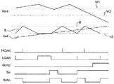
このような構成において、図2は、PWM制御時におけるスイッチングレギュレータ1の動作例を示したタイミングチャートである。図2を参照しながらPWM制御時における図1の回路の動作について説明する。なお、iLはインダクタL1に流れるインダクタ電流を示しており、第1電流値i1は、ハイサイド電流検出回路11に設定された電流値であり、PWM制御時の基準電流をなしている。
ハイサイド電流検出回路11は、制御回路8からPWM制御を行うことを示す選択信号Selectが入力されると、前記ハイサイド電流と第1電流値i1との比較を行い、前記ハイサイド電流が第1電流値i1以上である間、信号HCdetをハイレベルにする。
In such a configuration, FIG. 2 is a timing chart showing an operation example of the switching regulator 1 during PWM control. The operation of the circuit of FIG. 1 during PWM control will be described with reference to FIG. Note that iL indicates the inductor current flowing through the inductor L1, and the first current value i1 is a current value set in the high-side
When the selection signal Select indicating that PWM control is performed is input from the control circuit 8, the high side
電流パルス制御回路14は、PWMパルス信号Spwmがハイレベルに立ち上がると電流パルス信号Scpをハイレベルに立ち上げ、PWMパルス信号Spwmの立ち下がり、又は信号HCdetの立ち上がりのいずれか早い方のタイミングで電流パルス信号Scpをローレベルに立ち下げる。
位相検出回路15は、入力された電流パルス信号ScpとPWMパルス信号Spwmとの位相比較を行い、位相が一致した場合にハイレベルの出力信号Spsを出力する。
制御回路8は、PWM制御を行うときは、第2コンパレータ10の出力信号Scmpの立ち下がりにより選択信号Selectをローレベルにし、VFM制御を行うときは、出力信号Spsの立ち上がりにより選択信号Selectをハイレベルにする。
When the PWM pulse signal Spwm rises to a high level, the current
The
When the PWM control is performed, the control circuit 8 sets the selection signal Select to the low level by the falling edge of the output signal Scmp of the
クロック信号CLKのパルスP1〜P3のサイクルでは、電流パルス制御回路14は、ハイサイド電流検出回路11から出力された信号HCdetによって電流パルス信号Scpのハイレベルのパルス幅を決定し、パルスP4のサイクルでは、PWMパルス信号Spwmの立ち下がりによって電流パルス信号Scpのハイレベルのパルス幅を決定する。クロック信号CLKのパルスの立ち上がりをPWM制御時のフレーム初期サイクルとすると、該フレーム初期サイクルにおけるインダクタ電流iLの電流値をi0とし、PWM制御時の基準電流値である第1電流値i1はハイサイド電流検出用の電流値をなしており、出力端子OUTに負荷が接続されたときの各サイクルの出力端子OUTから出力される負荷電流である出力電流ioutは、下記(1)式のようになる。
iout=i0+(i1−i0)/2………………(1)
In the cycle of pulses P1 to P3 of the clock signal CLK, the current
iout = i0 + (i1-i0) / 2 (1)
位相検出回路15の出力信号Spsは、PWM制御からVFM制御へと切り換える制御信号でもあることから、PWMパルス信号Spwmと電流パルス信号Scpの位相が一致して、ハイレベルの出力信号Spsを出力する状態では、PWM制御時のハイサイド電流値は、第1電流値i1未満であり、1サイクル時の出力電流ioutは、前記(1)式で示した値以下の状態であることが分かる。特に、PWM制御時のハイサイド電流におけるピーク電流値が、第1電流値i1で設定したインダクタ電流iL以下で動作する条件で、PWM制御が不連続モードとなるように設定した場合では、電流値i0はゼロになるため、前記(1)式は下記(2)式のようになり、出力電流ioutは、i1/2以下になる。
iout=i1/2………………(2)
Since the output signal Sps of the
iout = i1 / 2 (2)
このように、PWM制御からVFM制御に切り換わる際の出力電流ioutは、ハイサイド電流検出回路11に設定された第1電流値i1の1/2以下となり、第1電流値i1を設定することによって、PWM制御からVFM制御に切り換わる際の出力電流ioutの電流値を設定することができる。
Thus, the output current iout when switching from PWM control to VFM control is ½ or less of the first current value i1 set in the high-side
次に、図3は、VFM制御時におけるスイッチングレギュレータ1の動作例を示したタイミングチャートである。図3を参照しながらVFM制御時における図1の回路の動作例について説明する。
第2電流値i2は、ハイサイド電流検出回路11に設定されたVFM制御時の基準電流値を示し、第3電流値i3は、ローサイド電流検出回路12に設定されたVFM制御時の基準電流値を示している。
ハイサイド電流検出回路11は、制御回路8からVFM制御を行うことを示す選択信号Selectが入力されると、前記ハイサイド電流と第2電流値i2との比較を行い、前記ハイサイド電流が第2電流値i2以上である間、信号HCdetをハイレベルにする。
また、ローサイド電流検出回路12は、前記ローサイド電流と第3電流値i3との比較を行い、ローサイド電流が第3電流値i3以下である間、ハイレベルの信号LCdetを出力する。
Next, FIG. 3 is a timing chart showing an operation example of the switching regulator 1 during the VFM control. An example of operation of the circuit of FIG. 1 during VFM control will be described with reference to FIG.
The second current value i2 indicates a reference current value at the time of VFM control set in the high-side
When the selection signal Select indicating that the VFM control is performed from the control circuit 8, the high side
The low-side
VFMパルス制御回路13は、第1コンパレータ3からハイレベルの出力信号Seが出力されている期間、前記ローサイド電流と第3電流値i3との比較結果を示した信号である信号LCdetの立ち上がりに応じてVFMパルス信号Svfmをハイレベルにし、選択信号Selectによって選択された第2電流値i2との比較信号である信号HCdetの立ち上がりに応じてVFMパルス信号Svfmをローレベルにする。また、VFMパルス制御回路13は、第1コンパレータ3からの出力信号Seが立ち上がった際に、信号LCdetが立ち上がらない場合は、出力信号Seが立ち上がったときにVFMパルス信号Svfmをハイレベルに立ち上げる。
The VFM
VFM制御時にハイレベルのVFMパルス信号Svfmが連続して出力されている状態では、インダクタ電流iLは、第2電流値i2又は第3電流値i3のいずれかと等価になる。このような状態では、第2コンパレータ10の出力信号Scmpがハイレベルになった場合、第2電流値i2と第3電流値i3との平均値以上の出力電流ioutが流れていることになる。すなわち、第2コンパレータ10が出力電圧Voutの低下を検出したときの出力電流ioutは、下記(3)式のようになる。
iout>(i2−i3)/2………………(3)
In a state where the high-level VFM pulse signal Svfm is continuously output during the VFM control, the inductor current iL is equivalent to either the second current value i2 or the third current value i3. In such a state, when the output signal Scmp of the
iout> (i2-i3) / 2 (3)
すなわち、VFM制御からPWM制御へ切り換わるときの出力電流ioutは、電流値(i2−i3)の1/2以上になっていると判断することができる。
このように、VFM制御からPWM制御に切り換わる際の出力電流ioutの電流値を、ハイサイド電流検出回路11の第2電流値i2及びローサイド電流検出回路12の第3電流値i3を設定することによって設定することができる。
That is, it can be determined that the output current iout when switching from the VFM control to the PWM control is equal to or greater than ½ of the current value (i2-i3).
As described above, the current value of the output current iout when switching from VFM control to PWM control is set to the second current value i2 of the high-side
このように、本第1の実施の形態におけるスイッチングレギュレータは、ハイサイド電流検出回路11の第1電流値i1を設定することによって、PWM制御からVFM制御に切り換わる際の出力電流ioutの電流値を設定することができると共に、VFM制御からPWM制御に切り換わる際の出力電流ioutの電流値を、ハイサイド電流検出回路11の第2電流値i2及びローサイド電流検出回路12の第3電流値i3を設定することによって設定することができ、出力電流検出用抵抗を使用することなく、PWM制御とVFM制御の切り換わり時における負荷電流値を正確に設定することができる。
As described above, the switching regulator according to the first embodiment sets the first current value i1 of the high-side
なお、前記説明では、同期整流方式の降圧型スイッチングレギュレータを例にして説明したが、これは一例であり、本発明はこれに限定するものではなく、非同期整流方式の降圧型スイッチングレギュレータや、昇圧型スイッチングレギュレータや、反転型スイッチングレギュレータ等にも適用することができる。
また、前記第1の実施の形態におけるスイッチングレギュレータを他の回路と共に1つの半導体装置を形成するようにしてもよく、該半導体装置は、ICをなすようにしてもよい。
In the above description, the synchronous rectification step-down switching regulator has been described as an example. However, this is only an example, and the present invention is not limited thereto. The present invention can also be applied to a type switching regulator, an inverting type switching regulator, and the like.
Further, the switching regulator in the first embodiment may be formed together with other circuits to form one semiconductor device, and the semiconductor device may form an IC.
1 スイッチングレギュレータ
2 第1基準電圧発生回路
3 第1コンパレータ
4 位相補償回路
5 発振回路
6 スロープ回路
7 PWMコンパレータ
8 制御回路
9 第2基準電圧発生回路
10 第2コンパレータ
11 ハイサイド電流検出回路
12 ローサイド電流検出回路
13 VFMパルス制御回路
14 電流パルス制御回路
15 位相検出回路
M1 スイッチングトランジスタ
M2 同期整流用トランジスタ
L1 インダクタ
C1 出力コンデンサ
R1,R2 抵抗
DESCRIPTION OF SYMBOLS 1 Switching regulator 2 1st reference voltage generation circuit 3 1st comparator 4 Phase compensation circuit 5
Claims (8)
入力された制御信号に応じてスイッチングを行うスイッチ素子と、
該スイッチ素子のスイッチングによって前記入力電圧による充電が行われるインダクタと、
前記スイッチ素子がオフして該インダクタへの充電が停止すると、該インダクタの放電を行う整流素子と、
前記出力電圧に比例した比例電圧と所定の第1基準電圧との電圧比較を行い、該比較結果を示す信号を出力すると共に該各電圧の電圧差を増幅して誤差電圧を生成し出力する誤差増幅回路部と、
前記誤差電圧をPWM変調して、前記PWM制御を行うためのPWMパルス信号を生成し出力するPWMパルス生成回路部と、
前記スイッチ素子を流れる電流であるハイサイド電流と、前記整流素子を流れる電流であるローサイド電流の検出を行い、該検出結果を示す信号を生成して出力する電流検出回路部と、
前記出力電圧の検出を行い、該出力電圧が所定値以下に低下したことを検出すると所定の信号を出力する出力電圧低下検出回路部と、
前記PWMパルス信号における前記スイッチ素子をオンさせるタイミングを示したエッジと、前記電流検出回路部の出力信号におけるハイサイド電流が所定値になったことを示すエッジとの間隔のパルス幅を有する電流パルス信号を生成して出力する電流パルス生成回路部と、
前記PWMパルス信号と該電流パルス信号との各位相を比較し、該比較結果を示す信号を生成して出力する位相検出回路部と、
前記電流検出回路部の出力信号から、VFM制御を行うためのVFMパルス信号を生成して出力するVFMパルス生成回路部と、
前記PWMパルス信号を使用したPWM制御又は該VFMパルス信号を使用したVFM制御のいずれかの制御で前記スイッチ素子のスイッチング制御を行うスイッチング制御回路部と、
を備え、
前記スイッチング制御回路部は、前記位相検出回路部の出力信号に応じてPWM制御からVFM制御への切り換えを行い、前記出力電圧低下検出回路部の出力信号に応じてVFM制御からPWM制御への切り換えを行うことを特徴とするスイッチングレギュレータ。 In a switching regulator that automatically switches between PWM control and VFM control, converts an input voltage input to an input terminal to a predetermined constant voltage, and outputs the voltage as an output voltage from the output terminal.
A switching element that performs switching according to the input control signal;
An inductor that is charged by the input voltage by switching of the switch element;
When the switching element is turned off and charging to the inductor is stopped, the rectifying element that discharges the inductor;
An error in which a proportional voltage proportional to the output voltage is compared with a predetermined first reference voltage, a signal indicating the comparison result is output, and an error voltage is generated by amplifying the voltage difference between the voltages. An amplification circuit section;
A PWM pulse generation circuit unit that PWM-modulates the error voltage and generates and outputs a PWM pulse signal for performing the PWM control;
A current detection circuit unit that detects a high-side current that flows through the switch element and a low-side current that flows through the rectifier element, generates a signal indicating the detection result, and outputs the signal;
An output voltage drop detection circuit unit that detects the output voltage and outputs a predetermined signal when detecting that the output voltage has decreased below a predetermined value;
A current pulse having a pulse width of an interval between an edge indicating the timing for turning on the switch element in the PWM pulse signal and an edge indicating that the high-side current in the output signal of the current detection circuit unit has reached a predetermined value. A current pulse generation circuit for generating and outputting a signal;
A phase detection circuit unit for comparing each phase of the PWM pulse signal and the current pulse signal, and generating and outputting a signal indicating the comparison result;
A VFM pulse generation circuit unit that generates and outputs a VFM pulse signal for performing VFM control from an output signal of the current detection circuit unit;
A switching control circuit unit that performs switching control of the switch element by either PWM control using the PWM pulse signal or VFM control using the VFM pulse signal;
With
The switching control circuit unit switches from PWM control to VFM control according to the output signal of the phase detection circuit unit, and switches from VFM control to PWM control according to the output signal of the output voltage drop detection circuit unit. The switching regulator characterized by performing.
Priority Applications (2)
| Application Number | Priority Date | Filing Date | Title |
|---|---|---|---|
| JP2008167147A JP5091028B2 (en) | 2008-06-26 | 2008-06-26 | Switching regulator and semiconductor device including the switching regulator |
| US12/488,694 US8258765B2 (en) | 2008-06-26 | 2009-06-22 | Switching regulator and semiconductor apparatus including the same |
Applications Claiming Priority (1)
| Application Number | Priority Date | Filing Date | Title |
|---|---|---|---|
| JP2008167147A JP5091028B2 (en) | 2008-06-26 | 2008-06-26 | Switching regulator and semiconductor device including the switching regulator |
Publications (2)
| Publication Number | Publication Date |
|---|---|
| JP2010011617A JP2010011617A (en) | 2010-01-14 |
| JP5091028B2 true JP5091028B2 (en) | 2012-12-05 |
Family
ID=41446578
Family Applications (1)
| Application Number | Title | Priority Date | Filing Date |
|---|---|---|---|
| JP2008167147A Expired - Fee Related JP5091028B2 (en) | 2008-06-26 | 2008-06-26 | Switching regulator and semiconductor device including the switching regulator |
Country Status (2)
| Country | Link |
|---|---|
| US (1) | US8258765B2 (en) |
| JP (1) | JP5091028B2 (en) |
Families Citing this family (17)
| Publication number | Priority date | Publication date | Assignee | Title |
|---|---|---|---|---|
| CN101471602B (en) * | 2007-12-29 | 2012-11-07 | 比亚迪股份有限公司 | Bidirectional DC power supply circuit |
| JP5169498B2 (en) | 2008-06-02 | 2013-03-27 | 株式会社リコー | Current detection circuit and switching regulator including the current detection circuit |
| US8300441B2 (en) * | 2009-05-04 | 2012-10-30 | Bc Systems, Inc | Active centerpoint power bus balancing system |
| US8638079B2 (en) * | 2010-02-27 | 2014-01-28 | Infineon Technologies Ag | Pulse modulation control in a DC-DC converter circuit |
| US9203301B2 (en) * | 2010-06-23 | 2015-12-01 | Volterra Semiconductor Corporation | Feedback for controlling the switching frequency of a voltage regulator |
| US8779744B2 (en) | 2010-07-27 | 2014-07-15 | Volterra Semiconductor Corporation | Sensing and feedback with enhanced stability in a current mode control voltage regulator |
| US9531266B2 (en) * | 2011-02-23 | 2016-12-27 | Infineon Technologies Americas Corp. | Power supply circuitry and adaptive transient control |
| US8803499B2 (en) * | 2011-02-23 | 2014-08-12 | International Recifier Corporation | Power supply circuitry and adaptive transient control |
| US8878509B2 (en) * | 2012-08-17 | 2014-11-04 | St-Ericsson Sa | Current-mode controller for step-down (buck) converter |
| JP6034132B2 (en) * | 2012-10-24 | 2016-11-30 | 株式会社ソニー・インタラクティブエンタテインメント | DC / DC converter and game machine using the same |
| US10698432B2 (en) * | 2013-03-13 | 2020-06-30 | Intel Corporation | Dual loop digital low drop regulator and current sharing control apparatus for distributable voltage regulators |
| KR102194973B1 (en) | 2014-01-28 | 2020-12-24 | 삼성전자주식회사 | Voltage converter and power management device including the same |
| DE102015204021B4 (en) * | 2015-03-05 | 2017-04-06 | Dialog Semiconductor (Uk) Limited | Dynamic current limiting circuit |
| KR102393214B1 (en) * | 2017-03-31 | 2022-05-02 | 삼성전기주식회사 | Apparatus for driving actuator |
| US10886856B2 (en) * | 2017-10-03 | 2021-01-05 | Delta Electronics, Inc. | Power converter and power converter control method |
| US10574138B2 (en) * | 2017-10-03 | 2020-02-25 | Delta Electronics, Inc. | Power converter, power converting system, and power converter control method |
| CN108418427B (en) | 2018-02-13 | 2020-07-14 | 昂宝电子(上海)有限公司 | System and method for adjusting one or more thresholds in a power converter |
Family Cites Families (28)
| Publication number | Priority date | Publication date | Assignee | Title |
|---|---|---|---|---|
| US5568044A (en) * | 1994-09-27 | 1996-10-22 | Micrel, Inc. | Voltage regulator that operates in either PWM or PFM mode |
| JP3647811B2 (en) * | 2002-01-22 | 2005-05-18 | 東北パイオニア株式会社 | DC-DC converter circuit |
| JP4106979B2 (en) * | 2002-06-25 | 2008-06-25 | ソニー株式会社 | Electronic equipment |
| JP4110926B2 (en) * | 2002-07-11 | 2008-07-02 | 富士電機デバイステクノロジー株式会社 | DC-DC converter |
| US7940033B2 (en) * | 2003-04-22 | 2011-05-10 | Aivaka, Inc. | Control loop for switching power converters |
| JP2005080366A (en) * | 2003-08-29 | 2005-03-24 | Matsushita Electric Ind Co Ltd | Switching power supply |
| TWI255088B (en) * | 2004-05-24 | 2006-05-11 | Anpec Electronics Corp | DC converting controller with mode-switching and over-current protection by using multifunctional pin and its method |
| US7382114B2 (en) * | 2005-06-07 | 2008-06-03 | Intersil Americas Inc. | PFM-PWM DC-DC converter providing DC offset correction to PWM error amplifier and equalizing regulated voltage conditions when transitioning between PFM and PWM modes |
| US7327127B2 (en) * | 2005-06-17 | 2008-02-05 | Via Technologies, Inc. | Pulse-frequency mode DC-DC converter circuit |
| JP2007209103A (en) | 2006-02-01 | 2007-08-16 | Ricoh Co Ltd | Current mode control dc-dc converter |
| JP4899528B2 (en) * | 2006-02-24 | 2012-03-21 | セイコーエプソン株式会社 | Power supply |
| JP4878181B2 (en) | 2006-03-06 | 2012-02-15 | 株式会社リコー | Current detection circuit and current mode DC-DC converter using the current detection circuit |
| JP2007252137A (en) | 2006-03-17 | 2007-09-27 | Ricoh Co Ltd | Non-insulated step-down type dc-dc converter |
| US7990120B2 (en) * | 2006-08-04 | 2011-08-02 | Linear Technology Corporation | Circuits and methods for adjustable peak inductor current and hysteresis for burst mode in switching regulators |
| JP5014714B2 (en) * | 2006-09-12 | 2012-08-29 | 株式会社リコー | Switching regulator and switching regulator control circuit |
| JP4926625B2 (en) | 2006-09-14 | 2012-05-09 | 株式会社リコー | Switching regulator and semiconductor device having the switching regulator |
| JP4928202B2 (en) | 2006-09-14 | 2012-05-09 | 株式会社リコー | Slope compensation circuit and switching regulator |
| JP2008079378A (en) * | 2006-09-19 | 2008-04-03 | Toshiba Corp | Electronic equipment |
| JP2008099385A (en) * | 2006-10-10 | 2008-04-24 | Toshiba Corp | Dc-dc converter |
| JP2008131747A (en) | 2006-11-21 | 2008-06-05 | Ricoh Co Ltd | Step-up/down switching regulator and its operation control method |
| JP2008131746A (en) | 2006-11-21 | 2008-06-05 | Ricoh Co Ltd | Step-up/down switching regulator |
| JP2008178263A (en) | 2007-01-22 | 2008-07-31 | Ricoh Co Ltd | Step-up/step-down switching regulator, and reverse-current prevention method for the step-up/step-down switching regulator |
| JP2008206366A (en) | 2007-02-22 | 2008-09-04 | Ricoh Co Ltd | Voltage rise/fall type switching regulator |
| JP2008228514A (en) | 2007-03-15 | 2008-09-25 | Ricoh Co Ltd | Switching regulator and operation control method therefor |
| JP2007252197A (en) | 2007-05-02 | 2007-09-27 | Ricoh Co Ltd | Non-insulated step-down type dc-dc converter |
| JP5151266B2 (en) | 2007-06-20 | 2013-02-27 | 株式会社リコー | Switching regulator and switching regulator operation control method |
| US20090079408A1 (en) * | 2007-09-21 | 2009-03-26 | Nexem, Inc. | Voltage mode pwmff-pfm/skip combo controller |
| JP4700679B2 (en) | 2007-12-17 | 2011-06-15 | 株式会社リコー | Manufacturing method of toner for developing electrostatic image, toner, image forming apparatus and container |
-
2008
- 2008-06-26 JP JP2008167147A patent/JP5091028B2/en not_active Expired - Fee Related
-
2009
- 2009-06-22 US US12/488,694 patent/US8258765B2/en not_active Expired - Fee Related
Also Published As
| Publication number | Publication date |
|---|---|
| US20090322298A1 (en) | 2009-12-31 |
| US8258765B2 (en) | 2012-09-04 |
| JP2010011617A (en) | 2010-01-14 |
Similar Documents
| Publication | Publication Date | Title |
|---|---|---|
| JP5091028B2 (en) | Switching regulator and semiconductor device including the switching regulator | |
| JP4926625B2 (en) | Switching regulator and semiconductor device having the switching regulator | |
| JP5504685B2 (en) | Switching regulator and operation control method thereof | |
| JP5195182B2 (en) | Current mode control switching regulator | |
| US7804285B2 (en) | Control of operation of switching regulator to select PWM control or PFM control based on phase comparison | |
| KR100945437B1 (en) | Switching regulator | |
| JP5211959B2 (en) | DC-DC converter | |
| US7522432B2 (en) | Switching regulator and control circuit and method used therein | |
| JP5091027B2 (en) | Switching regulator | |
| US20090174384A1 (en) | Switching regulator and method of controlling the same | |
| KR101131262B1 (en) | Current mode control type switching regulator | |
| US7538526B2 (en) | Switching regulator, and a circuit and method for controlling the switching regulator | |
| US8803500B2 (en) | PFM SMPS with quick sudden load change response | |
| US7876077B2 (en) | Control circuit and control method of current mode control type DC-DC converter | |
| KR20150131116A (en) | Systems and methods for 100 percent duty cycle in switching regulators | |
| JP2010088218A (en) | Dc/dc converter | |
| JP2009225642A (en) | Power supply apparatus and semiconductor integrated circuit apparatus | |
| JP2004208448A (en) | Step-up/step-down dc-dc converter | |
| JP2006166667A (en) | Switching regulator | |
| JP6153732B2 (en) | Switching regulator | |
| KR20130009674A (en) | Switching mode power supply comprising slope compensation circuit |
Legal Events
| Date | Code | Title | Description |
|---|---|---|---|
| A621 | Written request for application examination |
Free format text: JAPANESE INTERMEDIATE CODE: A621 Effective date: 20110113 |
|
| A977 | Report on retrieval |
Free format text: JAPANESE INTERMEDIATE CODE: A971007 Effective date: 20120725 |
|
| TRDD | Decision of grant or rejection written | ||
| A01 | Written decision to grant a patent or to grant a registration (utility model) |
Free format text: JAPANESE INTERMEDIATE CODE: A01 Effective date: 20120821 |
|
| A01 | Written decision to grant a patent or to grant a registration (utility model) |
Free format text: JAPANESE INTERMEDIATE CODE: A01 |
|
| A61 | First payment of annual fees (during grant procedure) |
Free format text: JAPANESE INTERMEDIATE CODE: A61 Effective date: 20120913 |
|
| FPAY | Renewal fee payment (event date is renewal date of database) |
Free format text: PAYMENT UNTIL: 20150921 Year of fee payment: 3 |
|
| R150 | Certificate of patent or registration of utility model |
Free format text: JAPANESE INTERMEDIATE CODE: R150 |
|
| LAPS | Cancellation because of no payment of annual fees |