JP5082993B2 - High frequency power amplifier - Google Patents
High frequency power amplifier Download PDFInfo
- Publication number
- JP5082993B2 JP5082993B2 JP2008096944A JP2008096944A JP5082993B2 JP 5082993 B2 JP5082993 B2 JP 5082993B2 JP 2008096944 A JP2008096944 A JP 2008096944A JP 2008096944 A JP2008096944 A JP 2008096944A JP 5082993 B2 JP5082993 B2 JP 5082993B2
- Authority
- JP
- Japan
- Prior art keywords
- switch
- amplifier
- output terminal
- output
- capacitor
- Prior art date
- Legal status (The legal status is an assumption and is not a legal conclusion. Google has not performed a legal analysis and makes no representation as to the accuracy of the status listed.)
- Active
Links
- 239000003990 capacitor Substances 0.000 claims description 34
- 238000010586 diagram Methods 0.000 description 10
- 230000000694 effects Effects 0.000 description 2
Images


Classifications
-
- H—ELECTRICITY
- H03—ELECTRONIC CIRCUITRY
- H03F—AMPLIFIERS
- H03F3/00—Amplifiers with only discharge tubes or only semiconductor devices as amplifying elements
- H03F3/189—High-frequency amplifiers, e.g. radio frequency amplifiers
- H03F3/19—High-frequency amplifiers, e.g. radio frequency amplifiers with semiconductor devices only
-
- H—ELECTRICITY
- H03—ELECTRONIC CIRCUITRY
- H03F—AMPLIFIERS
- H03F3/00—Amplifiers with only discharge tubes or only semiconductor devices as amplifying elements
- H03F3/72—Gated amplifiers, i.e. amplifiers which are rendered operative or inoperative by means of a control signal
-
- H—ELECTRICITY
- H03—ELECTRONIC CIRCUITRY
- H03F—AMPLIFIERS
- H03F2200/00—Indexing scheme relating to amplifiers
- H03F2200/421—Multiple switches coupled in the output circuit of an amplifier are controlled by a circuit
-
- H—ELECTRICITY
- H03—ELECTRONIC CIRCUITRY
- H03F—AMPLIFIERS
- H03F2200/00—Indexing scheme relating to amplifiers
- H03F2200/451—Indexing scheme relating to amplifiers the amplifier being a radio frequency amplifier
-
- H—ELECTRICITY
- H03—ELECTRONIC CIRCUITRY
- H03F—AMPLIFIERS
- H03F2203/00—Indexing scheme relating to amplifiers with only discharge tubes or only semiconductor devices as amplifying elements covered by H03F3/00
- H03F2203/72—Indexing scheme relating to gated amplifiers, i.e. amplifiers which are rendered operative or inoperative by means of a control signal
- H03F2203/7221—Indexing scheme relating to gated amplifiers, i.e. amplifiers which are rendered operative or inoperative by means of a control signal the gated amplifier being switched on or off by a switch at the output of the amplifier
-
- H—ELECTRICITY
- H03—ELECTRONIC CIRCUITRY
- H03F—AMPLIFIERS
- H03F2203/00—Indexing scheme relating to amplifiers with only discharge tubes or only semiconductor devices as amplifying elements covered by H03F3/00
- H03F2203/72—Indexing scheme relating to gated amplifiers, i.e. amplifiers which are rendered operative or inoperative by means of a control signal
- H03F2203/7239—Indexing scheme relating to gated amplifiers, i.e. amplifiers which are rendered operative or inoperative by means of a control signal the gated amplifier being switched on or off by putting into parallel or not, by choosing between amplifiers and shunting lines by one or more switch(es)
Landscapes
- Engineering & Computer Science (AREA)
- Power Engineering (AREA)
- Amplifiers (AREA)
Description
本発明は、増幅器を通る経路と増幅器を迂回する経路とをスイッチにより切り替える高周波電力増幅器に関し、特に通過損失を低減することができる高周波電力増幅器に関するものである。 The present invention relates to a high-frequency power amplifier that switches a path that passes through an amplifier and a path that bypasses the amplifier by a switch, and more particularly to a high-frequency power amplifier that can reduce passage loss.
増幅器を通る経路と増幅器を迂回する経路とをスイッチにより切り替える高周波電力増幅器が提案されている(例えば、特許文献1参照)。
図5は、高周波電力増幅器の参考例を示すブロック図である。増幅器10は、第1の入力端子IN1から入力した信号を増幅して出力端子OUTに出力する。バイパス経路12は、増幅器10を介さずに第2の入力端子IN2と出力端子OUTを接続する。増幅器10のゲートは入力整合回路14を介して第1の入力端子IN1に接続され、増幅器10のドレインはインダクタ16を介して電源端子Vcに接続され、増幅器10のソースは接地されている。コンデンサ34の一端は出力整合回路18を介して増幅器10のドレインに接続され、コンデンサ34の他端は出力端子OUTに接続されている。スイッチ36は、制御部28により制御されて、高出力時にはコンデンサ34の他端と出力端子OUTを接続し、低出力時にはバイパス経路12と出力端子OUTを接続する。
FIG. 5 is a block diagram showing a reference example of the high-frequency power amplifier. The
図5の高周波電力増幅器では、高出力時に増幅器10から出力された信号はスイッチ36を介して出力端子OUTに出力されるため、スイッチ36において通過損失が生じるという問題があった。また、特許文献1の回路では、増幅器と出力端子の間にあるサーキュレータにおいて同様に通過損失が生じるという問題があった。これらのスイッチ36やサーキュレータにおける通過損失分を増幅器10で補正しなければならないため、出力電力が同じ単体の増幅器と比べて動作電流が増加するという問題があった。
The high-frequency power amplifier of FIG. 5 has a problem in that a pass loss occurs in the
本発明は、上述のような課題を解決するためになされたもので、その目的は通過損失を低減することができる高周波電力増幅器を得るものである。 The present invention has been made to solve the above-described problems, and an object of the present invention is to obtain a high-frequency power amplifier capable of reducing the passage loss.
本発明に係る高周波電力増幅器は、第1の入力端子から入力した信号を増幅して出力端子に出力する増幅器と、増幅器を介さずに第2の入力端子と出力端子を接続するバイパス経路と、一端が増幅器に接続され、他端が出力端子に接続されたコンデンサと、一端がコンデンサの他端及び出力端子に接続され、他端がバイパス経路に接続された第1のスイッチと、コンデンサに並列に接続されたインダクタと、コンデンサに並列に接続され、インダクタに直列に接続された第2のスイッチと、高出力時には第1のスイッチ及び第2のスイッチをOFFにし、低出力時には第1のスイッチ及び第2のスイッチをONにする制御部とを備える。本発明のその他の特徴は以下に明らかにする。 A high frequency power amplifier according to the present invention includes an amplifier that amplifies a signal input from a first input terminal and outputs the amplified signal to an output terminal, a bypass path that connects the second input terminal and the output terminal without passing through the amplifier, A capacitor having one end connected to the amplifier and the other end connected to the output terminal, a first switch connected to the other end of the capacitor and the output terminal, and the other end connected to the bypass path, and the capacitor in parallel And a second switch connected in parallel to the capacitor and connected in series with the inductor, the first switch and the second switch are turned off at high output, and the first switch at low output And a control unit for turning on the second switch. Other features of the present invention will become apparent below.
本発明により、通過損失を低減することができる。 According to the present invention, passage loss can be reduced.
実施の形態1.
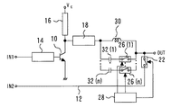
図1は、実施の形態1に係る高周波電力増幅器を示すブロック図である。増幅器10は、第1の入力端子IN1から入力した信号を増幅して出力端子OUTに出力する。バイパス経路12は、増幅器10を介さずに第2の入力端子IN2と出力端子OUTを接続する。
FIG. 1 is a block diagram showing a high frequency power amplifier according to the first embodiment. The
増幅器10のゲートは入力整合回路14を介して第1の入力端子IN1に接続され、増幅器10のドレインはインダクタ16を介して電源端子Vcに接続され、増幅器10のソースは接地されている。コンデンサ20の一端は出力整合回路18を介して増幅器10のドレインに接続され、コンデンサ20の他端は出力端子OUTに接続されている。
The gate of the
第1のスイッチ22の一端はコンデンサ20の他端及び出力端子OUTに接続され、第1のスイッチ22の他端はバイパス経路12に接続されている。
One end of the
インダクタ24はコンデンサ20に並列に接続されている。第2のスイッチ26は、コンデンサ20に並列に接続され、インダクタ24に直列に接続されている。制御部28は第1のスイッチ22及び第2のスイッチ26のON/OFFを制御する。
The
上記の高周波電力増幅器の動作について説明する。高出力時には、制御部28は第1のスイッチ22及び第2のスイッチ26をOFFにする。このように第2のスイッチ26がOFFであるため、第2のスイッチ26による通過損失は影響しない。また、第1のスイッチ22がOFFであるため、バイパス経路12側は増幅器10側から分離される。従って、通過損失を低減することができる。従って、出力電力が同じ単体増幅器と比べて動作電流を同程度に抑えることができる。なお、コンデンサ20は出力整合回路18の一部として動作する。
The operation of the high frequency power amplifier will be described. At the time of high output, the
低出力時には、制御部28は第1のスイッチ22及び第2のスイッチ26をONにする。これにより、第2の入力端子IN2から入力された信号は、増幅器10を介することなく出力端子OUTから出力される。この際に、コンデンサ20とインダクタ24からなるLC共振回路は入力された信号の周波数で共振し、バイパス経路12から増幅器10側を見たインピーダンスが高くなり、バイパス経路12から増幅器10側が分離される。この結果、バイパス経路12の通過損失をほぼ第1のスイッチ22による通過損失だけに抑えることができる。
At the time of low output, the
実施の形態2.
図2は、実施の形態2に係る高周波電力増幅器を示すブロック図である。実施の形態1のコンデンサ20の代わりにインダクタ30が設けられ、実施の形態1のインダクタ24の代わりにコンデンサ32が設けられている。その他の構成は実施の形態1の構成と同じである。これにより、実施の形態1と同様の効果を得ることができる。
Embodiment 2. FIG.
FIG. 2 is a block diagram showing a high-frequency power amplifier according to the second embodiment. An
実施の形態3.
図3は、実施の形態3に係る高周波電力増幅器を示すブロック図である。実施の形態1のインダクタ24の代わりに複数のインダクタ24(1)〜24(n)がコンデンサ20にそれぞれ並列に接続されている。実施の形態1の第2のスイッチ26の代わりに複数の第2のスイッチ26(1)〜26(n)がコンデンサ20にそれぞれ並列に接続され、複数のインダクタ24(1)〜24(n)にそれぞれ直列に接続されている。制御部28は、高出力時には第1のスイッチ22及び複数の第2のスイッチ26(1)〜26(n)をOFFにし、低出力時には第1のスイッチ22及び複数の第2のスイッチ26(1)〜26(n)をONにする。その他の構成は実施の形態1の構成と同じである。
Embodiment 3 FIG.
FIG. 3 is a block diagram showing a high frequency power amplifier according to the third embodiment. A plurality of inductors 24 (1) to 24 (n) are connected in parallel to the
第2の入力端子IN2から入力される信号の周波数帯域が広い場合、上記のように複数のインダクタ24(1)〜24(n)と複数の第2のスイッチ26(1)〜26(n)で共振周波数を重ねて設計することにより、広帯域にわたって通過損失を低減することができる。 When the frequency band of the signal input from the second input terminal IN2 is wide, the plurality of inductors 24 (1) to 24 (n) and the plurality of second switches 26 (1) to 26 (n) as described above. By designing with overlapping resonance frequencies, it is possible to reduce the passage loss over a wide band.
実施の形態4.
図4は、実施の形態4に係る高周波電力増幅器を示すブロック図である。実施の形態2のコンデンサ32の代わりに複数のコンデンサ32(1)〜32(n)がインダクタ30にそれぞれ並列に接続されている。実施の形態2の第2のスイッチ26の代わりに複数の第2のスイッチ26(1)〜26(n)がインダクタ30にそれぞれ並列に接続され、複数のコンデンサ32(1)〜32(n)にそれぞれ直列に接続されている。制御部28は、高出力時には第1のスイッチ22及び複数の第2のスイッチ26(1)〜26(n)をOFFにし、低出力時には第1のスイッチ22及び複数の第2のスイッチ26(1)〜26(n)をONにする。その他の構成は実施の形態2の構成と同じである。これにより、実施の形態3と同様の効果を得ることができる。
Embodiment 4 FIG.
FIG. 4 is a block diagram showing a high-frequency power amplifier according to the fourth embodiment. A plurality of capacitors 32 (1) to 32 (n) are connected to the
10 増幅器
12 バイパス経路
20,32,32(1)〜32(n) コンデンサ
22 第1のスイッチ
24,24(1)〜24(n),30 インダクタ
26,26(1)〜26(n) 第2のスイッチ
28 制御部
IN1 第1の入力端子
IN2 第2の入力端子
OUT 出力端子
10
Claims (4)
前記増幅器を介さずに第2の入力端子と前記出力端子を接続するバイパス経路と、
一端が前記増幅器に接続され、他端が前記出力端子に接続されたコンデンサと、
一端が前記コンデンサの他端及び前記出力端子に接続され、他端が前記バイパス経路に接続された第1のスイッチと、
前記コンデンサに並列に接続されたインダクタと、
前記コンデンサに並列に接続され、前記インダクタに直列に接続された第2のスイッチと、
高出力時には前記第1のスイッチ及び前記第2のスイッチをOFFにし、低出力時には前記第1のスイッチ及び前記第2のスイッチをONにする制御部とを備えることを特徴とする高周波電力増幅器。 An amplifier that amplifies the signal input from the first input terminal and outputs the amplified signal to the output terminal;
A bypass path connecting the second input terminal and the output terminal without going through the amplifier;
A capacitor having one end connected to the amplifier and the other end connected to the output terminal;
A first switch having one end connected to the other end of the capacitor and the output terminal and the other end connected to the bypass path;
An inductor connected in parallel with the capacitor;
A second switch connected in parallel to the capacitor and connected in series to the inductor;
A high-frequency power amplifier comprising: a control unit that turns off the first switch and the second switch at high output and turns on the first switch and the second switch at low output.
前記増幅器を介さずに第2の入力端子と前記出力端子を接続するバイパス経路と、
一端が前記増幅器に接続され、他端が前記出力端子に接続されたインダクタと、
一端が前記インダクタの他端及び前記出力端子に接続され、他端が前記バイパス経路に接続された第1のスイッチと、
前記インダクタに並列に接続されたコンデンサと、
前記インダクタに並列に接続され、前記コンデンサに直列に接続された第2のスイッチと、
高出力時には前記第1のスイッチ及び前記第2のスイッチをOFFにし、低出力時には前記第1のスイッチ及び前記第2のスイッチをONにする制御部とを備えることを特徴とする高周波電力増幅器。 An amplifier that amplifies the signal input from the first input terminal and outputs the amplified signal to the output terminal;
A bypass path connecting the second input terminal and the output terminal without going through the amplifier;
An inductor having one end connected to the amplifier and the other end connected to the output terminal;
A first switch having one end connected to the other end of the inductor and the output terminal and the other end connected to the bypass path;
A capacitor connected in parallel to the inductor;
A second switch connected in parallel to the inductor and connected in series to the capacitor;
A high-frequency power amplifier comprising: a control unit that turns off the first switch and the second switch at high output and turns on the first switch and the second switch at low output.
前記増幅器を介さずに第2の入力端子と前記出力端子を接続するバイパス経路と、
一端が前記増幅器に接続され、他端が前記出力端子に接続されたコンデンサと、
一端が前記コンデンサの他端及び前記出力端子に接続され、他端が前記バイパス経路に接続された第1のスイッチと、
前記コンデンサにそれぞれ並列に接続された複数のインダクタと、
前記コンデンサにそれぞれ並列に接続され、前記複数のインダクタにそれぞれ直列に接続された複数の第2のスイッチと、
高出力時には前記第1のスイッチ及び前記複数の第2のスイッチをOFFにし、低出力時には前記第1のスイッチ及び前記複数の第2のスイッチをONにする制御部とを備えることを特徴とする高周波電力増幅器。 An amplifier that amplifies the signal input from the first input terminal and outputs the amplified signal to the output terminal;
A bypass path connecting the second input terminal and the output terminal without going through the amplifier;
A capacitor having one end connected to the amplifier and the other end connected to the output terminal;
A first switch having one end connected to the other end of the capacitor and the output terminal and the other end connected to the bypass path;
A plurality of inductors each connected in parallel to the capacitor;
A plurality of second switches respectively connected in parallel to the capacitors and respectively connected in series to the plurality of inductors;
A control unit that turns off the first switch and the plurality of second switches at high output, and turns on the first switch and the plurality of second switches at low output. High frequency power amplifier.
前記増幅器を介さずに第2の入力端子と前記出力端子を接続するバイパス経路と、
一端が前記増幅器に接続され、他端が前記出力端子に接続されたインダクタと、
一端が前記インダクタの他端及び前記出力端子に接続され、他端が前記バイパス経路に接続された第1のスイッチと、
前記インダクタにそれぞれ並列に接続された複数のコンデンサと、
前記インダクタにそれぞれ並列に接続され、前記複数のコンデンサにそれぞれ直列に接続された第2のスイッチと、
高出力時には前記第1のスイッチ及び前記複数の第2のスイッチをOFFにし、低出力時には前記第1のスイッチ及び前記複数の第2のスイッチをONにする制御部とを備えることを特徴とする高周波電力増幅器。 An amplifier that amplifies the signal input from the first input terminal and outputs the amplified signal to the output terminal;
A bypass path connecting the second input terminal and the output terminal without going through the amplifier;
An inductor having one end connected to the amplifier and the other end connected to the output terminal;
A first switch having one end connected to the other end of the inductor and the output terminal and the other end connected to the bypass path;
A plurality of capacitors each connected in parallel to the inductor;
A second switch connected in parallel to each of the inductors and connected in series to the plurality of capacitors;
A control unit that turns off the first switch and the plurality of second switches at high output, and turns on the first switch and the plurality of second switches at low output. High frequency power amplifier.
Priority Applications (2)
| Application Number | Priority Date | Filing Date | Title |
|---|---|---|---|
| JP2008096944A JP5082993B2 (en) | 2008-04-03 | 2008-04-03 | High frequency power amplifier |
| US12/181,336 US7679441B2 (en) | 2008-04-03 | 2008-07-29 | High frequency power amplifier |
Applications Claiming Priority (1)
| Application Number | Priority Date | Filing Date | Title |
|---|---|---|---|
| JP2008096944A JP5082993B2 (en) | 2008-04-03 | 2008-04-03 | High frequency power amplifier |
Publications (2)
| Publication Number | Publication Date |
|---|---|
| JP2009253500A JP2009253500A (en) | 2009-10-29 |
| JP5082993B2 true JP5082993B2 (en) | 2012-11-28 |
Family
ID=41132697
Family Applications (1)
| Application Number | Title | Priority Date | Filing Date |
|---|---|---|---|
| JP2008096944A Active JP5082993B2 (en) | 2008-04-03 | 2008-04-03 | High frequency power amplifier |
Country Status (2)
| Country | Link |
|---|---|
| US (1) | US7679441B2 (en) |
| JP (1) | JP5082993B2 (en) |
Families Citing this family (3)
| Publication number | Priority date | Publication date | Assignee | Title |
|---|---|---|---|---|
| US8063698B2 (en) * | 2008-05-02 | 2011-11-22 | Bose Corporation | Bypassing amplification |
| US8325931B2 (en) * | 2008-05-02 | 2012-12-04 | Bose Corporation | Detecting a loudspeaker configuration |
| US20100062813A1 (en) * | 2008-09-10 | 2010-03-11 | Skyworks Solutions, Inc. | Power amplifier load line switch for a portable transceiver |
Family Cites Families (7)
| Publication number | Priority date | Publication date | Assignee | Title |
|---|---|---|---|---|
| JPH09148852A (en) * | 1995-11-24 | 1997-06-06 | Matsushita Electric Ind Co Ltd | Transmission output variable device |
| JP2000022559A (en) | 1998-07-03 | 2000-01-21 | Nec Corp | Transmission output control circuit |
| JP2002290157A (en) * | 2001-03-27 | 2002-10-04 | Mobile Communications Tokyo Inc | High-frequency power amplifier |
| JP4220694B2 (en) * | 2001-03-27 | 2009-02-04 | パナソニック株式会社 | High frequency variable gain amplifier |
| JP2004159102A (en) * | 2002-11-06 | 2004-06-03 | Mobile Communications Tokyo Inc | High-frequency power amplifier circuit |
| US7102444B2 (en) | 2004-01-20 | 2006-09-05 | Anadigics, Inc. | Method and apparatus for compensating and improving efficiency in a variable power amplifier |
| JPWO2006006244A1 (en) * | 2004-07-14 | 2008-04-24 | 三菱電機株式会社 | High power amplifier |
-
2008
- 2008-04-03 JP JP2008096944A patent/JP5082993B2/en active Active
- 2008-07-29 US US12/181,336 patent/US7679441B2/en active Active
Also Published As
| Publication number | Publication date |
|---|---|
| US7679441B2 (en) | 2010-03-16 |
| JP2009253500A (en) | 2009-10-29 |
| US20090251209A1 (en) | 2009-10-08 |
Similar Documents
| Publication | Publication Date | Title |
|---|---|---|
| JP6597461B2 (en) | Amplifier circuit | |
| JP6206698B2 (en) | Power amplifier | |
| US8098095B2 (en) | Power amplifier | |
| US8731490B2 (en) | Methods and circuits for detuning a filter and matching network at the output of a power amplifier | |
| JP5082993B2 (en) | High frequency power amplifier | |
| JP6112500B2 (en) | Microwave amplifier | |
| JP5425316B2 (en) | Output mode switching amplifier | |
| JP6342086B2 (en) | High frequency multistage amplifier | |
| JP5638426B2 (en) | Multistage amplifier | |
| JP2005260703A (en) | Power composite type amplifier | |
| JP2009118254A (en) | High-frequency signal output circuit | |
| KR101589587B1 (en) | T-type dual band impedance matching circuit and the design method thereof | |
| JP5161856B2 (en) | Bias circuit | |
| JP4936963B2 (en) | Variable frequency amplifier | |
| JP6056515B2 (en) | Power amplifier module | |
| US10148239B1 (en) | Circuit with co-matching topology for transmitting and receiving RF signals | |
| JP5349119B2 (en) | High frequency amplifier | |
| JP2007228034A (en) | High frequency amplifier | |
| JP2012257111A (en) | Active circuit | |
| KR101599782B1 (en) | Power amplifier and method of operating power amplifier | |
| KR102316430B1 (en) | Phase shifter | |
| JP2011023841A (en) | Wideband variable gain amplifier | |
| JP2012060275A (en) | High-frequency power amplifier | |
| JP5099908B2 (en) | Doherty synthesis circuit and Doherty amplifier | |
| JP6797041B2 (en) | Low noise amplifier |
Legal Events
| Date | Code | Title | Description |
|---|---|---|---|
| A621 | Written request for application examination |
Free format text: JAPANESE INTERMEDIATE CODE: A621 Effective date: 20110317 |
|
| A977 | Report on retrieval |
Free format text: JAPANESE INTERMEDIATE CODE: A971007 Effective date: 20120118 |
|
| TRDD | Decision of grant or rejection written | ||
| A01 | Written decision to grant a patent or to grant a registration (utility model) |
Free format text: JAPANESE INTERMEDIATE CODE: A01 Effective date: 20120807 |
|
| A01 | Written decision to grant a patent or to grant a registration (utility model) |
Free format text: JAPANESE INTERMEDIATE CODE: A01 |
|
| A61 | First payment of annual fees (during grant procedure) |
Free format text: JAPANESE INTERMEDIATE CODE: A61 Effective date: 20120820 |
|
| R150 | Certificate of patent or registration of utility model |
Ref document number: 5082993 Country of ref document: JP Free format text: JAPANESE INTERMEDIATE CODE: R150 Free format text: JAPANESE INTERMEDIATE CODE: R150 |
|
| FPAY | Renewal fee payment (event date is renewal date of database) |
Free format text: PAYMENT UNTIL: 20150914 Year of fee payment: 3 |
|
| R250 | Receipt of annual fees |
Free format text: JAPANESE INTERMEDIATE CODE: R250 |
|
| R250 | Receipt of annual fees |
Free format text: JAPANESE INTERMEDIATE CODE: R250 |
|
| R250 | Receipt of annual fees |
Free format text: JAPANESE INTERMEDIATE CODE: R250 |
|
| R250 | Receipt of annual fees |
Free format text: JAPANESE INTERMEDIATE CODE: R250 |
|
| S111 | Request for change of ownership or part of ownership |
Free format text: JAPANESE INTERMEDIATE CODE: R313113 |
|
| R350 | Written notification of registration of transfer |
Free format text: JAPANESE INTERMEDIATE CODE: R350 |