JP5079611B2 - Semiconductor chip and semiconductor chip manufacturing method - Google Patents
Semiconductor chip and semiconductor chip manufacturing method Download PDFInfo
- Publication number
- JP5079611B2 JP5079611B2 JP2008180584A JP2008180584A JP5079611B2 JP 5079611 B2 JP5079611 B2 JP 5079611B2 JP 2008180584 A JP2008180584 A JP 2008180584A JP 2008180584 A JP2008180584 A JP 2008180584A JP 5079611 B2 JP5079611 B2 JP 5079611B2
- Authority
- JP
- Japan
- Prior art keywords
- layer
- semiconductor
- semiconductor chip
- contact
- current spreading
- Prior art date
- Legal status (The legal status is an assumption and is not a legal conclusion. Google has not performed a legal analysis and makes no representation as to the accuracy of the status listed.)
- Active
Links
Images


Classifications
-
- H—ELECTRICITY
- H01—ELECTRIC ELEMENTS
- H01L—SEMICONDUCTOR DEVICES NOT COVERED BY CLASS H10
- H01L33/00—Semiconductor devices with at least one potential-jump barrier or surface barrier specially adapted for light emission; Processes or apparatus specially adapted for the manufacture or treatment thereof or of parts thereof; Details thereof
- H01L33/02—Semiconductor devices with at least one potential-jump barrier or surface barrier specially adapted for light emission; Processes or apparatus specially adapted for the manufacture or treatment thereof or of parts thereof; Details thereof characterised by the semiconductor bodies
- H01L33/14—Semiconductor devices with at least one potential-jump barrier or surface barrier specially adapted for light emission; Processes or apparatus specially adapted for the manufacture or treatment thereof or of parts thereof; Details thereof characterised by the semiconductor bodies with a carrier transport control structure, e.g. highly-doped semiconductor layer or current-blocking structure
- H01L33/145—Semiconductor devices with at least one potential-jump barrier or surface barrier specially adapted for light emission; Processes or apparatus specially adapted for the manufacture or treatment thereof or of parts thereof; Details thereof characterised by the semiconductor bodies with a carrier transport control structure, e.g. highly-doped semiconductor layer or current-blocking structure with a current-blocking structure
-
- H—ELECTRICITY
- H01—ELECTRIC ELEMENTS
- H01L—SEMICONDUCTOR DEVICES NOT COVERED BY CLASS H10
- H01L33/00—Semiconductor devices with at least one potential-jump barrier or surface barrier specially adapted for light emission; Processes or apparatus specially adapted for the manufacture or treatment thereof or of parts thereof; Details thereof
- H01L33/02—Semiconductor devices with at least one potential-jump barrier or surface barrier specially adapted for light emission; Processes or apparatus specially adapted for the manufacture or treatment thereof or of parts thereof; Details thereof characterised by the semiconductor bodies
- H01L33/04—Semiconductor devices with at least one potential-jump barrier or surface barrier specially adapted for light emission; Processes or apparatus specially adapted for the manufacture or treatment thereof or of parts thereof; Details thereof characterised by the semiconductor bodies with a quantum effect structure or superlattice, e.g. tunnel junction
-
- H—ELECTRICITY
- H01—ELECTRIC ELEMENTS
- H01L—SEMICONDUCTOR DEVICES NOT COVERED BY CLASS H10
- H01L2924/00—Indexing scheme for arrangements or methods for connecting or disconnecting semiconductor or solid-state bodies as covered by H01L24/00
- H01L2924/0001—Technical content checked by a classifier
- H01L2924/0002—Not covered by any one of groups H01L24/00, H01L24/00 and H01L2224/00
-
- H—ELECTRICITY
- H01—ELECTRIC ELEMENTS
- H01L—SEMICONDUCTOR DEVICES NOT COVERED BY CLASS H10
- H01L33/00—Semiconductor devices with at least one potential-jump barrier or surface barrier specially adapted for light emission; Processes or apparatus specially adapted for the manufacture or treatment thereof or of parts thereof; Details thereof
- H01L33/36—Semiconductor devices with at least one potential-jump barrier or surface barrier specially adapted for light emission; Processes or apparatus specially adapted for the manufacture or treatment thereof or of parts thereof; Details thereof characterised by the electrodes
- H01L33/38—Semiconductor devices with at least one potential-jump barrier or surface barrier specially adapted for light emission; Processes or apparatus specially adapted for the manufacture or treatment thereof or of parts thereof; Details thereof characterised by the electrodes with a particular shape
- H01L33/385—Semiconductor devices with at least one potential-jump barrier or surface barrier specially adapted for light emission; Processes or apparatus specially adapted for the manufacture or treatment thereof or of parts thereof; Details thereof characterised by the electrodes with a particular shape the electrode extending at least partially onto a side surface of the semiconductor body
-
- H—ELECTRICITY
- H01—ELECTRIC ELEMENTS
- H01L—SEMICONDUCTOR DEVICES NOT COVERED BY CLASS H10
- H01L33/00—Semiconductor devices with at least one potential-jump barrier or surface barrier specially adapted for light emission; Processes or apparatus specially adapted for the manufacture or treatment thereof or of parts thereof; Details thereof
- H01L33/36—Semiconductor devices with at least one potential-jump barrier or surface barrier specially adapted for light emission; Processes or apparatus specially adapted for the manufacture or treatment thereof or of parts thereof; Details thereof characterised by the electrodes
- H01L33/38—Semiconductor devices with at least one potential-jump barrier or surface barrier specially adapted for light emission; Processes or apparatus specially adapted for the manufacture or treatment thereof or of parts thereof; Details thereof characterised by the electrodes with a particular shape
- H01L33/387—Semiconductor devices with at least one potential-jump barrier or surface barrier specially adapted for light emission; Processes or apparatus specially adapted for the manufacture or treatment thereof or of parts thereof; Details thereof characterised by the electrodes with a particular shape with a plurality of electrode regions in direct contact with the semiconductor body and being electrically interconnected by another electrode layer
-
- H—ELECTRICITY
- H01—ELECTRIC ELEMENTS
- H01L—SEMICONDUCTOR DEVICES NOT COVERED BY CLASS H10
- H01L33/00—Semiconductor devices with at least one potential-jump barrier or surface barrier specially adapted for light emission; Processes or apparatus specially adapted for the manufacture or treatment thereof or of parts thereof; Details thereof
- H01L33/36—Semiconductor devices with at least one potential-jump barrier or surface barrier specially adapted for light emission; Processes or apparatus specially adapted for the manufacture or treatment thereof or of parts thereof; Details thereof characterised by the electrodes
- H01L33/40—Materials therefor
- H01L33/405—Reflective materials
-
- H—ELECTRICITY
- H01—ELECTRIC ELEMENTS
- H01L—SEMICONDUCTOR DEVICES NOT COVERED BY CLASS H10
- H01L33/00—Semiconductor devices with at least one potential-jump barrier or surface barrier specially adapted for light emission; Processes or apparatus specially adapted for the manufacture or treatment thereof or of parts thereof; Details thereof
- H01L33/36—Semiconductor devices with at least one potential-jump barrier or surface barrier specially adapted for light emission; Processes or apparatus specially adapted for the manufacture or treatment thereof or of parts thereof; Details thereof characterised by the electrodes
- H01L33/40—Materials therefor
- H01L33/42—Transparent materials
Description
本発明は、半導体チップ及び半導体チップを製造する方法に関する。 The present invention relates to a semiconductor chip and a method for manufacturing the semiconductor chip.
LED半導体チップでは、取出効率、すなわち、半導体中で発生された放射電力に対する半導体から発出する放射電力の比は、多々ある損失過程により影響をこうむる。吸収損失は、とりわけ、取出効率の減少の原因となり得る。 In LED semiconductor chips, the extraction efficiency, i.e. the ratio of the radiated power emitted from the semiconductor to the radiated power generated in the semiconductor, is often affected by some loss process. Absorption losses can inter alia cause a reduction in extraction efficiency.
本発明の目的は、取出効率を向上させた半導体チップを明示することである。さらに、本発明は、高い取出効率を有する半導体チップの簡易な製造方法を明示するものである。 An object of the present invention is to clearly show a semiconductor chip with improved extraction efficiency. Furthermore, the present invention clearly shows a simple method for manufacturing a semiconductor chip having high extraction efficiency.
これらの目的は、請求項1に記載の半導体チップにより、及び請求項29に記載の方法によりそれぞれ達成される。従属請求項は、本発明の有利な構成と展開に関する。 These objects are achieved by the semiconductor chip according to claim 1 and by the method according to claim 29, respectively. The dependent claims relate to advantageous configurations and developments of the invention.
一つの実施形態によれば、本発明による半導体チップは、放射を発生するために設けられた活性領域を有する半導体連続層を有する半導体ボディを含んでなる。コンタクト部が、半導体ボディの上に配置される。注入障壁が、コンタクト部と活性領域の間に形成される。 According to one embodiment, a semiconductor chip according to the invention comprises a semiconductor body having a semiconductor continuous layer with an active region provided for generating radiation. A contact portion is disposed on the semiconductor body. An injection barrier is formed between the contact portion and the active region.
半導体チップの稼動中、コンタクト部から活性領域への電荷キャリアの垂直方向の注入は、注入障壁によって減少される。半導体チップの平面図において、電荷キャリアはコンタクト部の横に位置する活性領域へ大部分は注入される。この目的で、コンタクト部は、適切には、活性領域よりも縮小した横方向の広がりをもつ。コンタクト部の下では、反対に、電荷キャリアの活性領域への注入が減少される。このようにして、コンタクト部の下の活性領域で発生され、その後コンタクト部に吸収される放射の可能性を減少させることができる。言い換えれば、放射は半導体チップの活性領域において、垂直方向に放出された放射が上にあるコンタクト部によって吸収されず、むしろ半導体チップから発出できる横の領域で主に発生される。したがって、半導体チップの取出効率を増大することができる。 During operation of the semiconductor chip, vertical injection of charge carriers from the contact portion into the active region is reduced by the injection barrier. In the plan view of the semiconductor chip, most of the charge carriers are injected into the active region located beside the contact portion. For this purpose, the contact portion suitably has a lateral extent which is smaller than the active region. Under the contact, on the contrary, the injection of charge carriers into the active region is reduced. In this way, the possibility of radiation generated in the active region under the contact part and subsequently absorbed by the contact part can be reduced. In other words, radiation is mainly generated in the lateral region where radiation emitted in the vertical direction is not absorbed by the overlying contact portions in the active region of the semiconductor chip, but rather can be emitted from the semiconductor chip. Therefore, the semiconductor chip extraction efficiency can be increased.
一つの好適な構成では、注入障壁の横方向の形状は、コンタクト部の横方向の形状に適合される。半導体チップの平面図において、注入障壁はコンタクト部に好ましくは完全に重なることができる。さらに平面図において、注入障壁は、好ましくはコンタクト部と同じ基本的幾何学的形状をもつ。 In one preferred configuration, the lateral shape of the injection barrier is adapted to the lateral shape of the contact portion. In the plan view of the semiconductor chip, the injection barrier can preferably completely overlap the contact part. Further in plan view, the injection barrier preferably has the same basic geometric shape as the contact portion.
この場合に横方向は、半導体連続層の半導体層の主たる延在方向に沿って伸びる方向であると理解される。これに対して、垂直方向は、前記半導体層の主たる延在方向に対して垂直に交わる方向である。 In this case, the lateral direction is understood to be a direction extending along the main extending direction of the semiconductor layer of the semiconductor continuous layer. On the other hand, the vertical direction is a direction perpendicular to the main extending direction of the semiconductor layer.
一つの構成の変形では、注入障壁は、コンタクト部と半導体ボディの間の界面部に形成される。この場合には、注入障壁は、電位障壁によって、具体的にはショットキーコンタクト、すなわち、コンタクト部と半導体ボディ間の金属・半導体接合によって典型的に実現され得る。 In one configuration variant, the injection barrier is formed at the interface between the contact portion and the semiconductor body. In this case, the injection barrier can typically be realized by a potential barrier, specifically by a Schottky contact, that is, a metal-semiconductor junction between the contact portion and the semiconductor body.
さらに、注入障壁は、半導体ボディの凹部の中に形成することができる。一例では、コンタクト部に対して比較的低い接触抵抗をもつ半導体ボディの材料物質を凹部によって除去できる。その結果、コンタクト部に対してより高い接触抵抗をもつ半導体ボディの材料物質を露出することができる。このようにして、凹部に配置されたコンタクト部は、横方向よりも垂直方向で半導体ボディに対してより高い接触抵抗をもつことができる。コンタクト部から活性領域への直接的な垂直の注入が、このようにして低下される。 Furthermore, the injection barrier can be formed in a recess in the semiconductor body. In one example, the material material of the semiconductor body having a relatively low contact resistance with respect to the contact portion can be removed by the recess. As a result, the material substance of the semiconductor body having a higher contact resistance with respect to the contact portion can be exposed. In this way, the contact part arranged in the recess can have a higher contact resistance to the semiconductor body in the vertical direction than in the lateral direction. Direct vertical implantation from the contact to the active region is thus reduced.
この点で、金属コンタクトと半導体層の間の製造の指示により完全に回避できない接触抵抗、特に、線形のまたは少なくともほぼ線形の電流−電圧特性曲線を示すオーミック接触抵抗は、本発明の意味において注入障壁としてみなされないことに留意すべきである。むしろ、半導体チップの稼動中に外部電圧によってコンタクト部に印加された電荷キャリアが、半導体チップの平面図における注入障壁の領域では、活性領域へ注入されないように、または少なくとも、注入障壁の外側に比べてきわめて低い可能性で活性領域へ注入されるように、注入障壁は好ましくは形成される。この場合には、注入障壁は、活性領域よりも縮小した横方向の広がりをもつ。 In this respect, contact resistance that cannot be completely avoided by manufacturing instructions between the metal contact and the semiconductor layer, in particular ohmic contact resistance exhibiting a linear or at least approximately linear current-voltage characteristic curve, is injected in the sense of the present invention. It should be noted that it is not considered a barrier. Rather, charge carriers applied to the contact portion by an external voltage during operation of the semiconductor chip are not injected into the active region in the region of the injection barrier in the plan view of the semiconductor chip, or at least compared to the outside of the injection barrier. The injection barrier is preferably formed so that it is injected into the active region with a very low probability. In this case, the injection barrier has a lateral extent that is smaller than the active region.
代替的な構成の変形では、注入障壁は半導体ボディの中に形成される。好ましくは、注入障壁は、活性領域とコンタクト部の間に配置された半導体層の導電率が局部的に低下されている領域によって形成される。したがって、この領域における半導体層の導電率はこの領域外よりも低い。言い換えれば、この領域では、半導体層の横に隣接する領域に比べて導電率が減少されている。さらに、低下した導電率のこの領域は、横方向に好ましくは島のように形成され、その横方向の形状は、特に好ましくはコンタクト部の横方向の形状に適合される。 In an alternative configuration variant, the injection barrier is formed in the semiconductor body. Preferably, the injection barrier is formed by a region where the conductivity of the semiconductor layer disposed between the active region and the contact portion is locally lowered. Therefore, the conductivity of the semiconductor layer in this region is lower than outside this region. In other words, the conductivity is reduced in this region as compared to the region adjacent to the side of the semiconductor layer. Furthermore, this region of reduced conductivity is formed in the lateral direction, preferably like an island, and its lateral shape is particularly preferably adapted to the lateral shape of the contact part.
導電率が低下されている領域は、コンタクト部から垂直方向に隔てられている。この場合には、半導体チップの稼動中、電荷キャリアはコンタクト部から半導体ボディへ垂直方向に直接注入され得る。さらに活性領域へ達しようとする垂直の注入は、低い導電率のこの領域のために阻止される、または少なくとも、この領域外での注入の増加を有利にするよう減少される。したがって、半導体ボディの取出効率を増大することができる。 The region where the conductivity is lowered is separated from the contact portion in the vertical direction. In this case, during operation of the semiconductor chip, charge carriers can be directly injected vertically from the contact portion into the semiconductor body. In addition, vertical implantation that attempts to reach the active region is blocked for this region of low conductivity, or at least reduced to favor increased implantation outside this region. Therefore, the extraction efficiency of the semiconductor body can be increased.
さらに別の代替的な構成の変形では、注入障壁は半導体ボディの外側に形成される。好ましくは、注入障壁は、半導体ボディとコンタクト部の間に配置された絶縁層によって形成される。さらに、複数の絶縁層が半導体ボディとコンタクト部の間に形成され得る。特に好ましくは、複数の絶縁層がブラッグ反射鏡に従って形成される。したがって、誘電体反射鏡が絶縁層によって形成され得る。 In yet another alternative configuration variation, the injection barrier is formed outside the semiconductor body. Preferably, the injection barrier is formed by an insulating layer disposed between the semiconductor body and the contact portion. Furthermore, a plurality of insulating layers may be formed between the semiconductor body and the contact portion. Particularly preferably, the plurality of insulating layers are formed according to a Bragg reflector. Therefore, the dielectric reflector can be formed by the insulating layer.
注入障壁は、したがって、活性領域で発生された放射に対する反射鏡の機能をさらに果たすことができる。前記放射の吸収をしたがって大幅に減少させ得る。注入障壁、詳しく言えば誘電体反射鏡で反射された放射は、その後半導体チップから発出できる。したがって、半導体チップの取出効率をより大幅に増大することができる。 The injection barrier can thus further serve as a reflector for the radiation generated in the active region. The absorption of said radiation can therefore be greatly reduced. The radiation reflected by the injection barrier, specifically the dielectric mirror, can then be emitted from the semiconductor chip. Therefore, the extraction efficiency of the semiconductor chip can be greatly increased.
一つの好適な構成では、コンタクト部は、半導体ボディから遠い側のコンタクト部の縁面にコンタクト層を有する。コンタクト層は、例えば、ボンディングワイヤによる外部コンタクトと半導体チップとの接触を形成する役目をもつ。コンタクト層は、好ましくは、例えばAu、Ti、PtまたはNiといった金属または前記の物質の少なくとも一つを含んでなる金属合金を含有する。 In one preferred configuration, the contact portion has a contact layer on an edge surface of the contact portion far from the semiconductor body. The contact layer has a role of forming a contact between the external contact and the semiconductor chip by, for example, a bonding wire. The contact layer preferably contains a metal such as Au, Ti, Pt or Ni or a metal alloy comprising at least one of the aforementioned substances.
コンタクト部は、好ましくは、コンタクト層と半導体ボディの間に配置された反射鏡層を有する。反射鏡層は、好ましくは、活性領域で発生された放射に対する高い反射率をもつ。反射鏡層は、好ましくは、例えば、金、アルミニウム、銀、パラジウムまたはロジウムといった金属または上記の金属の少なくとも一つを含む金属合金を含有する。活性領域で発生された放射のコンタクト層での吸収は、反射鏡層によって回避できる。半導体チップの取出効率をこれにより増大できる。 The contact portion preferably has a reflecting mirror layer disposed between the contact layer and the semiconductor body. The reflector layer preferably has a high reflectivity for radiation generated in the active region. The reflector layer preferably contains a metal such as gold, aluminum, silver, palladium or rhodium, or a metal alloy containing at least one of the above metals. Absorption in the contact layer of radiation generated in the active region can be avoided by the reflector layer. Thereby, the extraction efficiency of the semiconductor chip can be increased.
コンタクト層は、少なくとも複数の横方向領域で反射鏡層よりも外側へ突出することができる。具体的には、コンタクト層は、横方向に反射鏡層にかぶさるように成形することができる。すなわち、コンタクト層は反射鏡層を少なくとも一つのその横の区域を覆う。コンタクト層から横方向にコンタクト層と境を接する層への電荷キャリアの直接注入が、このようにすれば簡単に行なえるようになる。この場合には、反射鏡層は、コンタクト部から半導体ボディへの電荷キャリアの注入には全く寄与しない、または少なくとも大きな寄与はしない。 The contact layer can protrude outward from the reflector layer in at least a plurality of lateral regions. Specifically, the contact layer can be formed so as to cover the reflector layer in the lateral direction. That is, the contact layer covers at least one lateral area of the reflector layer. In this way, direct injection of charge carriers from the contact layer to the layer bordering the contact layer in the lateral direction can be easily performed. In this case, the reflector layer does not contribute at all to the injection of charge carriers from the contact portion to the semiconductor body, or at least does not contribute significantly.
さらに、絶縁層または複数の絶縁層の活性領域から遠い側の面に反射鏡層を配置することができる。絶縁層により透過された放射をこのようにすれば反射鏡層によって反射することができる。活性領域で発生された放射に対する高い全反射率をもつ反射鏡集合体をこのようにして簡単に形成することができる。 Furthermore, a reflecting mirror layer can be disposed on the surface of the insulating layer or the plurality of insulating layers far from the active region. In this way, the radiation transmitted by the insulating layer can be reflected by the reflector layer. A reflector assembly with a high total reflectivity for the radiation generated in the active region can thus be simply formed.
一つの好適な構成では、半導体チップは、コンタクト部に電気的導通をもつように接続される電流拡散層を有する。半導体チップの稼動中、電流拡散層は、平面図において注入障壁の外側の活性領域に電荷キャリアを注入するために設けられる。 In one preferred configuration, the semiconductor chip has a current spreading layer connected to the contact portion so as to have electrical continuity. During operation of the semiconductor chip, a current spreading layer is provided for injecting charge carriers into the active region outside the injection barrier in plan view.
電流拡散層は、好ましくは、コンタクト部に比較して大きい横方向の広がりをもつ。電流拡散層は、特に好ましくは、活性領域を横方向に区切る半導体ボディの横側の領域と境を接する。活性領域への広い面域にわたる電荷キャリアの注入が、これにより簡単に行なわれる。 The current spreading layer preferably has a large lateral extent compared to the contact portion. The current spreading layer is particularly preferably in contact with the lateral region of the semiconductor body that divides the active region in the lateral direction. This facilitates the injection of charge carriers over a wide area into the active region.
一つの好適な構成では、電流拡散層は、コンタクト部がその中に配置される凹部を有する。凹部は、電流拡散層を垂直方向に通り抜けるように拡張することできる。コンタクト部から電流拡散層への電荷キャリアの垂直の注入をこれにより減少させることができる。 In one preferred configuration, the current spreading layer has a recess in which the contact portion is disposed. The recess can be extended to pass through the current spreading layer in the vertical direction. The vertical injection of charge carriers from the contact portion into the current spreading layer can thereby be reduced.
この場合には、電流拡散層とコンタクト部は、少なくとも複数の領域で互いに境を接することができる。したがって、電荷キャリアをコンタクト部から電流拡散層へ直接注入できる。 In this case, the current spreading layer and the contact portion can be in contact with each other in at least a plurality of regions. Therefore, charge carriers can be directly injected from the contact portion into the current diffusion layer.
代替として、電流拡散層とコンタクト部は、横方向に互いから隔てられるようにできる。この場合には、電流拡散層とコンタクト部は、好ましくは、コンタクト部と活性領域の間に配置された層によって電気的導通をもつように接続される。 Alternatively, the current spreading layer and the contact portion can be laterally separated from each other. In this case, the current spreading layer and the contact portion are preferably connected to have electrical continuity by a layer disposed between the contact portion and the active region.
さらに別の好適な構成では、電流拡散層は非金属である。さらに、電流拡散層は、好ましくは、活性領域で発生された放射に対して透過性である物質によって形成される。 In yet another preferred configuration, the current spreading layer is non-metallic. Furthermore, the current spreading layer is preferably formed by a material that is transparent to the radiation generated in the active region.
本発明の文脈では、非金属の電流拡散層は、層または連続層の個々の層が金属を含有できるが、前記層または複数の層が金属の特性をもたない層または連続層であると理解される。 In the context of the present invention, a non-metallic current spreading layer is a layer or continuous layer where individual layers can contain metal, but said layer or layers are layers or continuous layers that do not have metallic properties. Understood.
具体的には、非金属の電流拡散層は、半導体物質を基にする、または半導体物質からなることができる。電流拡散層は、したがって半導体ボディの中に形成され得る。この場合には、電流拡散層は好ましくは一つの半導体層であり、当該半導体層と活性領域の間に配置されたさらに別の半導体層とは導電型が異なる。 Specifically, the non-metallic current spreading layer can be based on or consist of a semiconductor material. A current spreading layer can thus be formed in the semiconductor body. In this case, the current spreading layer is preferably a single semiconductor layer and has a conductivity type different from that of another semiconductor layer disposed between the semiconductor layer and the active region.
代替として、電流拡散層は半導体ボディの外側に配置され得る。好ましくは、半導体ボディの外側に配置された電流拡散層は、TCO物質(透明導電性酸化物)を含有する。 Alternatively, the current spreading layer can be arranged outside the semiconductor body. Preferably, the current spreading layer disposed outside the semiconductor body contains a TCO material (transparent conductive oxide).
TCO物質は透明導電性酸化物であり、一般には、例えば、酸化亜鉛、酸化スズ、酸化カドミウム、酸化チタン、酸化インジウム、インジウムスズ酸化物(ITO)等の金属酸化物である。例えば、ZnO、SnO2またはIn2O3等の二元金属酸化物と共に、TCOのグループは、例えば、Zn2SnO4、CdSnO3、ZnSnO3、MgIn2O4、GaInO3、Zn2In2O5またはIn4Sn3O12等の三元金属酸化物、または異なる透明導電性酸化物の混合物も含む。さらにTCOは必ずしも化学量論的組成に一致しなくもよく、pまたはnドーピングすることもできる。 The TCO material is a transparent conductive oxide, and is generally a metal oxide such as, for example, zinc oxide, tin oxide, cadmium oxide, titanium oxide, indium oxide, indium tin oxide (ITO). For example, with binary metal oxides such as ZnO, SnO 2 or In 2 O 3 , TCO groups include, for example, Zn 2 SnO 4 , CdSnO 3 , ZnSnO 3 , MgIn 2 O 4 , GaInO 3 , Zn 2 In 2. Also included are ternary metal oxides such as O 5 or In 4 Sn 3 O 12 or mixtures of different transparent conductive oxides. Furthermore, the TCO does not necessarily match the stoichiometric composition and can be p-doped or n-doped.
さらに別の好適な構成では、接続層が電流拡散層と半導体ボディの間に配置される。接続層は、適切には、半導体層への低接触抵抗の導電性接続をもたらすために使用できる物質を含有する。好ましくは、接続層は、例えばチタン、プラチナ、ニッケル、ロジウムといった金属、または上記の金属の少なくとも一つを含んでなる金属合金を含有する。接続層は、さらに好ましくは、活性領域で発生された放射に対して少なくとも部分的に透過性であるように十分に薄くされる。特に好ましくは、接続層の厚さは最大でも10nmである。 In yet another preferred configuration, the connection layer is arranged between the current spreading layer and the semiconductor body. The connection layer suitably contains a material that can be used to provide a low contact resistance conductive connection to the semiconductor layer. Preferably, the connecting layer contains a metal such as titanium, platinum, nickel, rhodium, or a metal alloy comprising at least one of the above metals. The connection layer is more preferably made sufficiently thin so that it is at least partially transparent to the radiation generated in the active region. Particularly preferably, the thickness of the connection layer is at most 10 nm.
さらに別の好適な構成では、トンネルコンタクト層が電流拡散層と活性領域の間に配置される。トンネルコンタクト層は、当該トンネルコンタクト層と活性領域の間に配置されたさらに別の半導体層とは導電型が異なる。トンネルコンタクト層は、好ましくは高度にドーピングされた半導体層である。ドーピング濃度は、好ましくは、少なくとも1018cm−3、特に好ましくは、少なくとも1019cm−3である。 In yet another preferred configuration, a tunnel contact layer is disposed between the current spreading layer and the active region. The tunnel contact layer has a different conductivity type from another semiconductor layer disposed between the tunnel contact layer and the active region. The tunnel contact layer is preferably a highly doped semiconductor layer. The doping concentration is preferably at least 10 18 cm −3 , particularly preferably at least 10 19 cm −3 .
電流拡散層から活性領域への電荷キャリアの注入は、トンネルコンタクト層によって簡単に行なえるようになる。 The injection of charge carriers from the current spreading layer into the active region can be easily performed by the tunnel contact layer.
一つの好適な展開では、さらに別のトンネルコンタクト層が、トンネルコンタクト層の前記活性領域に対向する側の面に配置される。さらに別のトンネルコンタクト層は、トンネルコンタクト層とは異なる導電型をもつ。さらに、さらに別のトンネルコンタクト層は、好ましくは同様に高いドーピング濃度をもつ。 In one preferred development, a further tunnel contact layer is arranged on the surface of the tunnel contact layer facing the active region. Yet another tunnel contact layer has a different conductivity type than the tunnel contact layer. Furthermore, the further tunnel contact layer preferably has a high doping concentration as well.
さらに別の好適な展開では、注入障壁は、さらに別のトンネルコンタクト層の導電率が局部的に低下されている領域によって形成される。この場合には、注入障壁は、したがって半導体ボディの中に形成される。さらに、トンネルコンタクト層をコンタクト部とさらに別のトンネルコンタクト層の間に形成できる。したがって、局部的に低下された導電率の領域は、コンタクト部から垂直方向に隔てられるようにできる。半導体チップの稼動中、電荷キャリアは、したがってコンタクト部からトンネルコンタクト層へ移動し、横方向へ伝播できる。電荷キャリアの横方向の伝播は、さらに半導体ボディ内または外に配置された電流拡散層により促進され得る。トンネルコンタクト層から、電荷キャリアは次に、局部的に低下された導電率の領域の外側で、さらに別のトンネルコンタクト層を介して活性領域へ注入され得る。 In yet another preferred development, the injection barrier is formed by a region where the conductivity of the further tunnel contact layer is locally reduced. In this case, an injection barrier is thus formed in the semiconductor body. Furthermore, a tunnel contact layer can be formed between the contact portion and another tunnel contact layer. Accordingly, the locally reduced conductivity region can be separated from the contact portion in the vertical direction. During operation of the semiconductor chip, the charge carriers can therefore move from the contact part to the tunnel contact layer and propagate laterally. Lateral propagation of charge carriers can be further facilitated by a current spreading layer disposed in or out of the semiconductor body. From the tunnel contact layer, charge carriers can then be injected into the active region through yet another tunnel contact layer outside the region of locally reduced conductivity.
トンネルコンタクト層及び/またはさらに別のトンネルコンタクト層は、比較的薄くされ得る。その厚さは、100nm以下、好ましくは20nm以下、特に好ましくは10nmとすることができる。 The tunnel contact layer and / or the further tunnel contact layer may be relatively thin. The thickness can be 100 nm or less, preferably 20 nm or less, particularly preferably 10 nm.
一つの好適な構成では、電流拡散層はトンネルコンタクト層として実現される。電流拡散層は、したがって高度にドーピングされた半導体層であり、つまり半導体ボディの一部をなす。この場合には、電流拡散と電荷キャリアを活性領域に横方向に一様に印加するために半導体ボディの外側に配置されるさらに別の層は、省くことができる。 In one preferred configuration, the current spreading layer is realized as a tunnel contact layer. The current spreading layer is thus a highly doped semiconductor layer, ie it forms part of the semiconductor body. In this case, a further layer arranged outside the semiconductor body in order to apply current spreading and charge carriers uniformly in the lateral direction to the active region can be omitted.
トンネルコンタクト層の活性領域に対向する側の面にさらに別のトンネルコンタクト層を次に配置することができ、このさらに別のトンネルコンタクト層はトンネルコンタクト層とは異なる導電型をもつ。 A further tunnel contact layer can then be arranged on the surface of the tunnel contact layer facing the active region, the further tunnel contact layer having a conductivity type different from that of the tunnel contact layer.
半導体チップは、好ましくは、インコヒーレント放射または主としてインコヒーレント放射を発生させるように提供される。一例として、半導体チップをLEDチップとして、さらにRCLEDチップ(共振器型発光ダイオード)として実現することができる。RCLEDチップの場合は、活性領域はキャビティ内に配置される。 The semiconductor chip is preferably provided to generate incoherent radiation or primarily incoherent radiation. As an example, the semiconductor chip can be realized as an LED chip and further as an RCLED chip (resonator light emitting diode). In the case of an RCLED chip, the active region is located in the cavity.
半導体チップは、コヒーレント放射を発生させるように提供されてもよい。この場合には、半導体チップを半導体レーザチップとして、特に、内部共振器を有する面発光半導体レーザチップ(垂直キャビティ面発光レーザ、VCSEL)または外部の共振器と共に動作する面発光半導体チップ(垂直外部キャビティ面発光レーザ、VECSEL)として実現することができる。 The semiconductor chip may be provided to generate coherent radiation. In this case, the semiconductor chip is a semiconductor laser chip, in particular, a surface emitting semiconductor laser chip (vertical cavity surface emitting laser, VCSEL) having an internal resonator or a surface emitting semiconductor chip (vertical external cavity) operating with an external resonator. It can be realized as a surface emitting laser (VECSEL).
半導体ボディ、詳しく言えば活性領域は、好ましくは、III−V半導体物質を含有する。III−V半導体物質によって、高い効率の赤外線から紫外線までのスペクトル領域の放射を発生することが可能である。 The semiconductor body, in particular the active region, preferably contains a III-V semiconductor material. With III-V semiconductor materials, it is possible to generate highly efficient radiation in the spectral region from infrared to ultraviolet.
半導体チップ、詳しく言えば半導体ボディは、複数の活性領域、例えば、上下に重ねて配置された2つ以上の活性領域を有し得る。この場合には、半導体チップの上記の要素、具体的には電流拡散層、トンネルコンタクト層、さらに別のトンネルコンタクト層、及び接続層の活性領域に相対する配置は、コンタクト部に最も近い位置に配置される活性領域に関係する。 A semiconductor chip, in particular a semiconductor body, may have a plurality of active regions, for example two or more active regions arranged one above the other. In this case, the above-described elements of the semiconductor chip, specifically, the current diffusion layer, the tunnel contact layer, the further tunnel contact layer, and the arrangement of the connection layer relative to the active region are positioned closest to the contact portion. Related to the active area to be placed.
一つの実施形態によれば、放射を発生するために設けられた活性領域を有する半導体連続層を有する半導体ボディを含んでなる半導体チップを製造する本発明による方法において、半導体ボディの上にコンタクト部が形成される。活性領域とコンタクト部の間に注入障壁が形成される。 According to one embodiment, in a method according to the invention for manufacturing a semiconductor chip comprising a semiconductor body having a semiconductor continuous layer with an active region provided for generating radiation, a contact part on the semiconductor body is provided. Is formed. An injection barrier is formed between the active region and the contact portion.
一つの好適な構成では、注入障壁は半導体ボディの中に形成される。これは、詳しくは、コンタクト部が半導体ボディの上に形成される前に行なわれる。好ましくは、注入障壁は、半導体層の、当該半導体層の導電率が局部的に低下されている領域によって形成される。 In one preferred configuration, the injection barrier is formed in the semiconductor body. Specifically, this is performed before the contact portion is formed on the semiconductor body. Preferably, the injection barrier is formed by a region of the semiconductor layer where the conductivity of the semiconductor layer is locally reduced.
半導体層の導電率の局部的低下は、例えば水晶構造の標的を絞った外乱によるドーピングの補正によって、例えば、達成し得る。一例として、当初pドーピングされた半導体層に標的を絞ったやり方で生じさせた水晶の欠陥は、p型ドーピングの完全なまたは少なくとも部分的な補正を起こさせることができる。この場合には、p導電半導体層のアクセプタによって生じた導電率をドナーとして動作する欠陥によって減少させる。これは、例えば、バックスパッタリングによって実現できる。バックスパッタリング中、好ましくは、例えばArイオンビーム等のイオンビームが半導体層に当てられる。 A local decrease in the conductivity of the semiconductor layer can be achieved, for example, by correction of doping due to targeted disturbances of the quartz structure, for example. As an example, a crystal defect caused in a targeted manner to an initially p-doped semiconductor layer can cause complete or at least partial correction of p-type doping. In this case, the conductivity generated by the acceptor of the p conductive semiconductor layer is reduced by the defect operating as a donor. This can be achieved, for example, by back sputtering. During back sputtering, an ion beam such as an Ar ion beam is preferably applied to the semiconductor layer.
導電率の局部的低下は、ドナーまたはアクセプタの少なくとも一部を不活性化することによっても達成することができる。そこで、例えば、水素プラズマによってp型導電半導体層に水素を導入できる。p導電型にドーピングされたInGaAlNベースの半導体層中のアクセプタ、例えばMgアクセプタをこれにより電気的に不活性化できる。 A local decrease in conductivity can also be achieved by inactivating at least a portion of the donor or acceptor. Therefore, for example, hydrogen can be introduced into the p-type conductive semiconductor layer by hydrogen plasma. An acceptor, for example an Mg acceptor, in an InGaAlN-based semiconductor layer doped to p conductivity type can thereby be electrically deactivated.
当該半導体層に対して反対の電荷型をもつイオンの注入によって導電率を低下させることもできる。 The conductivity can also be reduced by implanting ions having the opposite charge type to the semiconductor layer.
さらに別の好適な実施形態では、例えば、スパッタリングまたは真空蒸着によって電流拡散層が半導体ボディに被着される。横方向パターニングマスク層が、電流拡散層の上に形成または配置され得る。その後、マスク層が存在しない領域において電流拡散層と半導体ボディの材料物質を除去できる。電流拡散層及び半導体ボディの横方向パターニングは、したがって共通のマスク層によって行なえる。したがって、追加のマスク層を省くことができる。その結果、製造コストを削減できる。さらに、これにより、パターニング精度を上げることができる。 In yet another preferred embodiment, the current spreading layer is deposited on the semiconductor body, for example by sputtering or vacuum deposition. A lateral patterning mask layer may be formed or disposed on the current spreading layer. Thereafter, the material of the current diffusion layer and the semiconductor body can be removed in the region where the mask layer does not exist. The lateral patterning of the current spreading layer and the semiconductor body can thus be performed by a common mask layer. Therefore, an additional mask layer can be omitted. As a result, the manufacturing cost can be reduced. Further, this can increase the patterning accuracy.
一つの好適な展開では、さらに別の横方向パターニングマスク層が電流拡散層の上に形成される。これは、好ましくはマスク層の除去の後に行なわれる。 In one preferred development, yet another lateral patterning mask layer is formed over the current spreading layer. This is preferably done after removal of the mask layer.
さらに別のマスク層が存在しないさらに別の領域において、電流拡散層に凹部を形成できる。反射鏡層と続いてコンタクト層を凹部に被着できる。 In a further region where there is no further mask layer, a recess can be formed in the current diffusion layer. A reflector layer and subsequently a contact layer can be deposited in the recess.
反射鏡層及びコンタクト層の形成における蒸着条件は、コンタクト層が横方向に反射鏡層よりも外に突出するように設定され得る。一例として、反射鏡層は垂直方向または実質的に垂直方向からを半導体ボディの上に蒸着可能であるが、コンタクト層は半導体ボディを同時に回転させつつ斜めから蒸着される。これにより達成できることは、コンタクト層が反射鏡層よりも大きい横方向の広がりをもつことであり、この目的のために異なるマスク層を用いる必要はない。 Vapor deposition conditions in forming the reflector layer and the contact layer can be set so that the contact layer protrudes outward from the reflector layer in the lateral direction. As an example, the reflector layer can be deposited on the semiconductor body vertically or substantially vertically, while the contact layer is deposited obliquely while rotating the semiconductor body simultaneously. What can be achieved by this is that the contact layer has a greater lateral extent than the reflector layer, and there is no need to use a different mask layer for this purpose.
さらに、コンタクト部またはコンタクト部の少なくとも一つの層、例えばコンタクト層または反射鏡層を、コンタクト部が電流拡散層から横方向に隔てられるように電流拡散層の凹部の中に形成できる。これは、上記の同じさらに別のマスク層によって行なえる。一例として、ウェット化学エッチングによって凹部を電流拡散層に形成できる。電流拡散層の凹部は、これにより、さらに別のマスク層の切欠き部よりも大きい横方向の広がりをとることができる。コンタクト部またはコンタクト部の少なくとも一つの層の横方向の広がりがさらに別のマスク層の切欠き部の横方向の広がり以下であるように、コンタクト部またはコンタクト部の少なくとも一つの層を次に蒸着することができる。これは、垂直方向または実質的に垂直方向からの蒸着におって行なえる。したがって、コンタクト部またはコンタクト部の少なくとも一つの層の間に少なくとも一つのすき間を形成することが可能である。 Furthermore, the contact portion or at least one layer of the contact portion, such as a contact layer or a reflector layer, can be formed in the recess of the current spreading layer such that the contact portion is laterally separated from the current spreading layer. This can be done with the same further mask layer described above. As an example, the recess can be formed in the current diffusion layer by wet chemical etching. Accordingly, the concave portion of the current spreading layer can have a larger lateral extent than a notch portion of another mask layer. The contact portion or at least one layer of the contact portion is then deposited so that the lateral extent of the contact portion or at least one layer of the contact portion is less than or equal to the lateral extent of the notch portion of the further mask layer. can do. This can be done in a vertical or substantially vertical deposition. Accordingly, it is possible to form at least one gap between the contact portion or at least one layer of the contact portion.
半導体ボディの上に配置された各層、具体的には、電流拡散層、コンタクト層、反射鏡層、接続層の形成は、好ましくは、真空蒸着またはスパッタリングによって行なわれる。 Formation of each layer disposed on the semiconductor body, specifically, the current diffusion layer, the contact layer, the reflector layer, and the connection layer is preferably performed by vacuum deposition or sputtering.
ここに述べた方法は、上述した半導体チップを製造するために特に適する。半導体チップに関連して説明した特徴はしたがって方法についても使用可能であるし、その逆も同様である。 The method described here is particularly suitable for manufacturing the semiconductor chip described above. The features described in connection with the semiconductor chip can therefore also be used for the method and vice versa.
本発明のさらに他の特徴、有利な構成及び有用性は、図面と併せて説明する例示的な実施形態の以下の記述から明らかになるであろう。 Still other features, advantageous configurations and utilities of the present invention will become apparent from the following description of exemplary embodiments described in conjunction with the drawings.
図において、同一の要素、同一の種類の要素、同一の働きをする要素には、同一の参照符号を付している。 In the figure, the same reference numerals are assigned to the same elements, the same types of elements, and the elements having the same functions.
これらの図はいずれも概略図であるので、必ずしも実寸大ではない。むしろ、比較的小さい要素、特に、薄い層については、明確化するために誇張した大きさで図示される要素もある。 Since these figures are all schematic, they are not necessarily full scale. Rather, for relatively small elements, particularly thin layers, some elements are shown in exaggerated size for clarity.
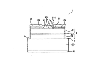
本発明による半導体チップの第1の例示的な実施形態を図1に断面図の形で概略的に示す。半導体チップ1は、半導体連続層をもつ半導体ボディ2を有する。半導体連続層が半導体ボディを形成する。半導体ボディは、p導電型半導体層21とn導電型半導体層22の間に配置された活性領域23を有する。
A first exemplary embodiment of a semiconductor chip according to the invention is schematically shown in cross-section in FIG. The semiconductor chip 1 has a
半導体ボディ2は、担持部20の上に配置される。担持部20は、例えば、半導体ボディ2の半導体連続層のための成長基板であり得る。一例として、担持部は、例えば、Si、Ge、GaAs、SiC、GaNまたはGaPを含有することができる、または上記の物質からなることができる。代替として、サファイアを含有する、またはサファイアからなる担持部を、例えば、適用することもできる。担持部は、導電率を上げるために適切にドーピングされ得る。成長基板上に半導体ボディ2の半導体連続層は、好ましくは、例えば、MBEまたはMOVPEによってエピタキシャルに蒸着される。
The
コンタクト部4が半導体ボディ2の上に配置される。コンタクト部は、活性領域23から見て担持部20とは反対側に配置され、例えば、円形または長方形の基本形状をもち得る。コンタクト部4は、コンタクト層41と反射鏡層42を有する。反射鏡層は、コンタクト層と半導体ボディ2の間に配置される。注入障壁5が、コンタクト部4と半導体ボディ2の間に形成される。
A
注入障壁は、担持部20から遠い側で半導体ボディの垂直方向の境界を定める、半導体ボディ2の界面部25に形成される。注入障壁は、コンタクト部4と半導体ボディ2の間のショットキーコンタクトとして、詳しく言えば、反射鏡層42とp導電型半導体層21の間のショットキーコンタクトとして実現される。この例では、注入障壁5の横方向の範囲は、コンタクト部4の横方向の範囲に一致する。
The injection barrier is formed at the
さらに、電流拡散層31が半導体ボディ2の上に配置される。電流拡散層31は、コンタクト部4と同じ側の半導体ボディ2の面に配置される。この例では、電流拡散層の横方向の範囲は、コンタクト部4の横方向の範囲に比較して大きい。電流拡散層31は、凹部310を有する。切欠き部分の垂直方向の範囲は、好ましくは、電流拡散層31を通り抜ける。コンタクト部4、詳しく言えばコンタクト層41が前記凹部に配置される。
Furthermore, the
コンタクト部4と電流拡散層31、詳しく言えば、コンタクト層41と電流拡散層31は横方向に互いに境を接する。半導体チップの稼動中にコンタクト層41へ注入された電荷キャリアは、したがって、横方向へコンタクト層41から電流拡散層31中へ直接移動することができる。電流拡散層31から、電荷キャリアは半導体ボディ、詳しくは、活性領域23へ垂直方向に注入され得る。一方、コンタクト層41から半導体ボディ2への直接の垂直方向の注入は、注入障壁5によってより困難にされる。半導体チップ1の平面図においては、したがって、注入障壁5の主に外側の活性領域において放射は発生される。半導体チップ1の取出効率は、これにより増大され得る。
The
電流拡散層31は、好ましくは非金属形態で実現され、さらに好ましくは、活性領域で発生された放射に対して透過性であるように形成される。電流拡散層31は、好ましくは、例えば、インジウムスズ酸化物(ITO)または酸化亜鉛(ZnO)といったTCO物質を含有する。さらに他の前述のTCO物質も電流拡散層31に適合し得る。
The current spreading
接続層32が、電流拡散層31と半導体ボディ2の間に形成される。接続層32によって、電荷キャリアを電流拡散層31から半導体ボディ2へ簡単に注入することができる。接続層があることにより、半導体ボディ2に対する低い、詳しくはオーミック接触抵抗を実現不可能であるような物質または実現できても困難を伴うような物質でも、したがって、電流拡散層に使用可能になる。電流拡散層31と半導体ボディ2の間の十分によい電気的接触が得られるならば、接続層はなくもよい。
A
接続層32は、好ましくは、金属形態でまたは金属合金を基にして実現される。さらに、接続層は好ましくは、活性領域で発生された放射が少なくとも部分的に接続層を通過できる程度に薄くされる。
The
接続層は、半導体層に対するよい接触特性を有する金属、例えば、チタン、プラチナ、ニッケル、ロジウムまたはその他の金属を含有することができる。代替的または補足的に、接続層は、好ましくは前述の物質の少なくとも一つを含んでなる金属合金を含有できる。プラチナは特に有利であることがわかった。接続層の厚さは、好ましくは、最大でも10nm、例えば3〜7nmである。一例として、6nmの厚さをもつプラチナ層は、青色スペクトル領域で約40%の透過率を有する。 The connection layer can contain a metal with good contact properties to the semiconductor layer, for example titanium, platinum, nickel, rhodium or other metals. Alternatively or additionally, the connecting layer can preferably contain a metal alloy comprising at least one of the aforementioned substances. Platinum has been found to be particularly advantageous. The thickness of the connection layer is preferably at most 10 nm, for example 3 to 7 nm. As an example, a platinum layer with a thickness of 6 nm has a transmission of about 40% in the blue spectral region.
半導体チップ1の平面図においては、注入障壁5はコンタクト部4よりも外側へ、好ましくは完全に外側へ突出する。これにより、半導体チップ1の稼動中にコンタクト部4へ注入された電荷キャリアが、注入障壁があるために、垂直方向に半導体ボディ2へ直接注入されない、またはごく少ない比率でしか直接注入されないことを確実にできる。電荷キャリアの圧倒的大部分は、コンタクト層41から横方向へ電流拡散層31中へと注入され、注入領域5外の接続層32を介してp導電型半導体層21へ入り、続いて活性領域23へ入る。したがって、コンタクト部4の下では、比較的わずかな電荷キャリアしか活性領域23へ注入されない。半導体の平面図においては、活性領域では、コンタクト部4の外側で主に、放射は電荷キャリア再結合により発生される。活性領域23で発生され、その後コンタクト部4によって吸収される放射の比率をこれにより低下させることができる。
In the plan view of the semiconductor chip 1, the
反射鏡層42は、コンタクト部、詳しく言えばコンタクト層41における吸収をさらに低下させる役目を担う。反射鏡層は、適切には、活性領域で発生される放射に対して可能な限り最高の反射率を有する物質により形成される。好ましくは、反射鏡層は、金属形態でまたは金属合金を基にして実現される。一例をあげると、金が赤外線及び赤色スペクトル領域に適しており、アルミニウム、銀、パラジウム及びロジウムが青色及び紫外線スペクトル領域において比較的高い反射率を有する。
The reflecting
コンタクト層41における活性領域23で発生された放射の吸収は、したがって反射鏡層42によって回避され得る。コンタクト層41用の材料物質は、したがって、例えば、ボンディングワイヤを用いた半導体チップのよい外部接触接続性を考慮して、光学特性とは概して無関係に選択可能である。具体的には、金属、例えば金、または金を含む合金、例えばAuSnが材料物質として適当である。
Absorption of radiation generated in the
さらに別のコンタクト部45が担持部20の半導体ボディ2から遠い側の面に配置される。コンタクト部4とさらに別のコンタクト部45の間に外部から電圧を印加することにより、電荷キャリアの活性領域への注入が可能となり、そこで発光と放射を伴う再結合が可能になる。
Further, another
半導体ボディ2、詳しく言えば活性領域23は、好ましくは、III−V半導体物質を含有する。III−V半導体物質は、紫外線(Inx Gay Al1−x−y N)から可視(詳しくは青色〜緑色放射用にはInx Gay Al1−x−y N、または詳しくは黄色から赤色放射用にはInx Gay Al1−x−y P)を通じ赤外線(Inx Gay Al1−x−y As)までにわたるスペクトル領域における放射を発生させるのに特に適している。ここで、0≦x≦1、0≦y≦1及びx+y≦1がいずれの場合にも当てはまり、詳しくはここで、x≠1、y≠1、x≠0及び/またはy≠0である。III−V半導体物質の使用により、特に前述の物質系から、放射の発生において高い内部量子効率をさらに得ることができる。
The
保護層7が半導体ボディ2の上に配置され、好ましくはその側面領域も含めて半導体ボディを覆う。前記保護層は、例えば、湿気等の有害な外部環境の影響から半導体ボディを保護する役目をする。しかし、このような保護層は絶対に必要なものではない。保護層は誘電方式でエピタキシャルに形成され、酸化物、例えば酸化シリコン、窒化物、例えば窒化シリコン、または酸窒化物、例えばシリコン酸窒化物を好ましくは含有する。
A
半導体層のドーピングは、本例示的な実施形態における一例として明示されるに過ぎない。特に、半導体層の導電型は、n型ドーピングされたものとして記述された半導体層がp型ドーピングされたり、p型ドーピングされたものとして記述された半導体層がn型ドーピングされたりするように、その変形では逆になり得る。 The doping of the semiconductor layer is only specified as an example in the present exemplary embodiment. In particular, the conductivity type of the semiconductor layer is such that the semiconductor layer described as n-type doped is p-type doped, or the semiconductor layer described as p-type doped is n-type doped. That variation can be reversed.
半導体チップ1はLED半導体として実現され、インコヒーレント放射を発生させるように提供される。その変形では、半導体チップをRCLED半導体チップとして実現することもできる。このような半導体チップでは、活性領域はキャビティ内に配置される。代替として、半導体チップを、コヒーレント放射を発生させるように実現することもできる。具体的には、面発光半導体レーザチップ(VCSEL)として、または外部の共振器において動作する面発光半導体チップ(VECSEL)として半導体チップを実現することができる。 The semiconductor chip 1 is realized as an LED semiconductor and is provided to generate incoherent radiation. In that variant, the semiconductor chip can also be realized as an RCLED semiconductor chip. In such a semiconductor chip, the active region is disposed in the cavity. Alternatively, the semiconductor chip can be implemented to generate coherent radiation. Specifically, the semiconductor chip can be realized as a surface emitting semiconductor laser chip (VCSEL) or a surface emitting semiconductor chip (VECSEL) that operates in an external resonator.
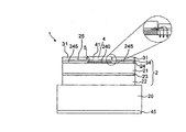
本発明による半導体チップの第2の例示的な実施形態を図2に概略的に示す。第2の例示的な実施形態は、図1に関連して説明した第1の例示的な実施形態と大体は同じである。第1の例示的な実施形態と対比して、半導体ボディ2はトンネルコンタクト層34とさらに別のトンネルコンタクト層24を追加して有する。トンネルコンタクト層とさらに別のトンネルコンタクト層はどちらも、好ましくは少なくとも1018cm−3、特に好ましくは少なくとも1019cm−3の高い電荷キャリアを有する。
A second exemplary embodiment of a semiconductor chip according to the present invention is schematically illustrated in FIG. The second exemplary embodiment is generally the same as the first exemplary embodiment described in connection with FIG. In contrast to the first exemplary embodiment, the
さらに、トンネルコンタクト層34とさらに別のトンネルコンタクト層24は、互いに反対の符号でドーピングされる。この例では、トンネルコンタクト層34は、活性領域23とトンネルコンタクト層の間に配置された半導体層21とは異なる導電型をもつ。一例として述べるケースでは、半導体層21はp型導電方式でドーピングされ、したがって、コンタクト層34はn型導電方式でドーピングされる。対応的に、さらに別のトンネルコンタクト層24は、境を接する半導体層21と同じくp型導電方式でドーピングされ、ここで、さらに別のトンネルコンタクト層24は半導体層21よりも高いドーピング濃度をもつ。
Furthermore, the
電流拡散層31は、トンネルコンタクト層の活性領域23から遠い側の面に形成される。電流拡散層31から半導体ボディ2への電荷キャリアの注入は、トンネルコンタクト層34とさらに別のトンネルコンタクト層24によって簡単に行なえるようになる。図1に関連して説明した第1の例示的な実施形態と対比して、したがって、半導体層は接続層の機能を果たす。半導体ボディ2と電流拡散層31の間に配置された追加の接続層は、これにより省くことができる。
The
さらに、第1の例示的な実施形態と対比して、注入障壁5は半導体ボディ2中に形成される。注入障壁5は、さらに別のトンネルコンタクト層24の一領域240となる。この領域でのさらに別のトンネルコンタクト層24は、さらに別のトンネルコンタクト層24の横方向に隣接する領域245に比べて低い導電率をもつ。半導体チップ1の平面図においては、コンタクト部4は、注入障壁5、すなわち、さらに別のトンネルコンタクト層24の領域240と一致した、または少なくとも実質的に一致した横方向に拡がる範囲をもつ。その形状がコンタクト部の形状に適合される注入障壁によって、コンタクト部4の下の活性領域への電荷キャリアの注入を特に効率的に低下させることができる。
Furthermore, in contrast to the first exemplary embodiment, the
トンネルコンタクト層34は、注入障壁5とコンタクト部4の間に配置される。コンタクト部4と注入障壁5、すなわち、低下した導電率の領域240は、したがって、垂直方向で互いから隔てられている。半導体チップ1の稼動中、電荷キャリアはコンタクト部4からトンネルコンタクト層34へ垂直方向に注入され得る。しかし、活性領域の方向へさらに垂直に移動する電荷キャリアの流れは、注入障壁によって回避される、または少なくとも大幅に減少される。
The
電荷キャリアの可能な注入経路を、矢印を用いて、図2の拡大抜き出し部に概略的に示す。電荷キャリアは、コンタクト部4からトンネルコンタクト層34を介して、半導体ボディの外側に配置された電流拡散層31へ移動することができる。前記電流拡散層では、電流は横方向へ拡散し、その後トンネルコンタクト層34を介して半導体ボディ2へ注入可能である。トンネルコンタクト層34の横導電率が比較的低い場合でも、このように広い面域にわたる電荷キャリアの注入が電流拡散層31によって可能になる。トンネルコンタクト層34は、したがって、非常に薄くすることができ、その厚さは、例えば、100nm以下、好ましくは20nm、特に好ましくは10nmであればよい。
Possible injection paths of charge carriers are schematically shown in the enlarged extraction part of FIG. 2 using arrows. The charge carriers can move from the
さらに、図1に関連して説明した第1の例示的な実施形態と対比して、コンタクト部4、詳しく言えばコンタクト層41は、横方向で電流拡散層31から隔てられている。したがって、コンタクト部と電流拡散層は、直接接続されるのではなく、トンネルコンタクト層34を介して互いに電気的導通をもつように接続される。第1の例示的な実施形態と対比して、したがって、電荷キャリアの半導体ボディへの注入は、コンタクト部4、詳しく言えばコンタクト層41が半導体ボディと境を接する、半導体ボディ2の界面部25の領域において生起される。この例では、コンタクト部4は、好ましくは、半導体ボディ2に対する低い接触抵抗を考慮して形成される。
Furthermore, in contrast to the first exemplary embodiment described in connection with FIG. 1, the
図2に示した半導体チップは、さらには、保護層を有しない。しかし、具体的には第1の例示的な実施形態で説明したように、このような保護層を提供し、実現することも同様に可能である。 The semiconductor chip shown in FIG. 2 further does not have a protective layer. However, it is equally possible to provide and implement such a protective layer, as specifically described in the first exemplary embodiment.
本発明による半導体チップの第3の例示的な実施形態を図3に概略断面図の形で示す。第3の例示的な実施形態は、図1に関連して説明した第1の例示的な実施形態と大体は同じである。これと対比して、図2に関連して説明したように、半導体ボディ2はトンネルコンタクト層34とさらに別のトンネルコンタクト層24を有する。
A third exemplary embodiment of a semiconductor chip according to the invention is shown in the form of a schematic sectional view in FIG. The third exemplary embodiment is generally the same as the first exemplary embodiment described in connection with FIG. In contrast, the
さらに、半導体ボディ2は凹部200を有する。p導電型半導体層21はこの切欠き部分によって露出される。トンネルコンタクト層34とさらに別のトンネルコンタクト層24は、したがって、コンタクト部4の領域内では除去される。p導電型半導体層21は、トンネルコンタクト層24、34よりも低いドーピング濃度をもつので、高電位の障壁、具体的にはショットキー障壁が、コンタクト部4、詳しく言えば反射鏡層42と半導体ボディ、詳しく言えばp導電型半導体層21の間に簡単に形成され得る。コンタクト部4から活性領域23への直接的な垂直の注入をこれにより低下することができる。
Further, the
図2に関連して説明したように、トンネルコンタクト層34とさらに別のトンネルコンタクト層24は、図1に関連して説明した第1の例示的な実施形態の接続層32の機能を果たす。半導体ボディ2の上に配置され、電流拡散層31と半導体ボディの間に置かれる接続層は、したがって備えられていない。
As described in connection with FIG. 2, the
半導体チップ1の稼動中、電荷キャリアはコンタクト層41へ注入される。ここから、電荷キャリアは、横方向でコンタクト層と直接境を接する電流拡散層31中へと横方向に移動する。電流拡散層から、電荷キャリアは半導体ボディ2へ垂直方向に注入され、ひいては活性領域23へと移動するが、コンタクト部の下の活性領域への注入はこの場合も低下される。
During operation of the semiconductor chip 1, charge carriers are injected into the
本発明による半導体チップの第4の例示的な実施形態を図4に概略断面図の形で示す。この第4の例示的な実施形態は、図1に関連して説明した第1の例示的な実施形態と大体は同じである。第1の例示的な実施形態と対比して、半導体ボディ2はトンネルコンタクト層34とさらに別のトンネルコンタクト層24を有する。トンネルコンタクト層34とさらに別のトンネルコンタクト層24は、p導電型半導体層21の上の全面域にわたり拡がる。
A fourth exemplary embodiment of a semiconductor chip according to the invention is shown in schematic cross-sectional view in FIG. This fourth exemplary embodiment is generally the same as the first exemplary embodiment described in connection with FIG. In contrast to the first exemplary embodiment, the
第4の例示的な実施形態では、注入障壁5は、半導体ボディ上に配置された複数の絶縁層51、52によって形成される。注入障壁は、したがって、半導体ボディ2の外側に配置され、少なくともコンタクト部4と半導体ボディ2の間の領域に置かれる。コンタクト部4から、絶縁層と境を接する、半導体ボディの領域への電荷キャリアの注入は、絶縁層によって簡単に回避され得る。
In the fourth exemplary embodiment, the
各絶縁層51と52は層ペアを形成するが、各層は互いに異なる屈折率を有する。ブラッグ反射鏡の形態の誘電体反射鏡が、前記層ペアによって形成される。半導体チップ1の稼動中に活性領域23で発生され、コンタクト部4の方向へ放出され、誘電体層51、52に入射する放射は、したがって、好ましくは少なくとも80%、特に好ましくは少なくとも90%の比較的高い反射率で、半導体ボディ方向へ戻るように反射され得る。前記放射は、その後半導体チップ1から発出する。半導体チップの取出効率をこのようにして増大することができる。層ペアの数がより多いほど、ブラッグ反射鏡の反射率をより高くすることができる。注入障壁は、したがって、非常に効率のよい反射鏡の機能を同時に果たすことができる。他方、絶縁層の数が増加するにつれて、蒸着期間も増大する。したがって、短い蒸着期間を特に考慮すれば、図示したこの例示的な実施形態の変形では、半導体ボディ2とコンタクト部4の間にただ一つの個別の絶縁層を形成してもよい。
Each insulating
コンタクト部4は、この場合も、コンタクト層41と反射鏡層42を有する。反射鏡層42は、絶縁層51、52の上を覆う。半導体チップ1の活性領域23で発生され、絶縁層51、52によって形成されたブラッグ反射鏡を透過した放射は、したがって、反射鏡層42から半導体ボディ2の方向へ戻るように反射され得る。特に高い全反射率を有する反射鏡が、ブラッグ反射鏡の上に半導体ボディから遠い側の面に配置された反射鏡層によって形成され得る。特に、ブラッグ反射鏡によって透過される放射の部分は、反射鏡層によって半導体ボディ2の方向へ戻るように反射可能であり、その後半導体チップ1から発出する。
The
さらに、図1に示した例示的な実施形態に対比して、コンタクト層41は、反射鏡層42よりも横方向の広がりが大きくなっている。したがって、コンタクト層41は、反射鏡層42の上に、特に完全にかぶさる形に成形できる。横方向にコンタクト層41は、したがって、電流拡散層31と注入障壁5、すなわち、絶縁層51,52の間に延在する。さらに、コンタクト層は、反射鏡層42と電流拡散層31の間に横方向に延在する。電荷キャリアは、これによりコンタクト層から電流拡散層へ簡単に直接移動することができる。可能な電流経路が、ここでも、図4に矢印を用いて示される。
Furthermore, in contrast to the exemplary embodiment shown in FIG. 1, the
この例では、絶縁層51、52によって形成されたブラッグ反射鏡の可能な限り最良の反射性被覆部を特に考慮して、前記反射鏡の半導体ボディから遠い側の面に、反射鏡層42は電気的接触特性とは無関係に形成され得る。
In this example, particularly considering the best possible reflective coating of the Bragg reflector formed by the insulating
本発明による半導体チップの第5の例示的な実施形態を図5に概略断面図を用いて示す。先の例示的な実施形態に対比して、電流拡散層31が半導体ボディ2中に組み込まれている。この例では、電流拡散層31はトンネルコンタクト層34によって形成される。コンタクト部4は、トンネルコンタクト層の活性領域23から遠い側の面の上に配置される。注入障壁5は、図2に関連して説明したように、トンネルコンタクト層24の一部の領域240によって形成される。この領域においては、さらに別のトンネルコンタクト層24の導電率が、この領域外、すなわち横に隣接する領域245よりも低い。この例示的な実施形態では、トンネルコンタクト層34は、十分に高い横導電率をもてるほどに厚くなっている。注入障壁5の外側での活性領域23への広い面域にわたる電荷キャリアの注入が、これにより簡単になる。半導体ボディの外側に配置される電流拡散層は、この例では省くことができる。
A fifth exemplary embodiment of a semiconductor chip according to the present invention is shown in FIG. In contrast to the previous exemplary embodiment, a current spreading
この例示的な実施形態では、コンタクト部4は、好ましくは、半導体ボディ2に対する可能な限り最低の、詳しくはオーミック接触抵抗をもつ。この目的で、コンタクト層41を多層に形成することもできる。一例として、半導体ボディから見て、チタン、プラチナ及び金の順に連続層がコンタクト層に適する。半導体チップの稼動中、電荷キャリアは、コンタクト部から最初に垂直方向に半導体ボディ2へ、詳しく言えば電流拡散層へ注入される。さらに活性領域へ達しようとする垂直の注入は、導電率の低い領域240によって減少される。
In this exemplary embodiment, the
コンタクト部4は、電流拡散層31の上に配置される。この例示的な実施形態では、電流拡散層は横方向のパターニングがない。したがって、半導体チップの製造が簡単になる。この変形では、しかし、電流拡散層に凹部を設けて、前記凹部にコンタクト部を配置することが可能である。
The
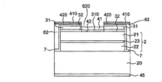
半導体チップの製造のための本発明による方法の第1の例示的な実施形態を、図6A〜6Eに断面図で概略的に示した数段階の中間工程に基づいて示す。図6Aに示すように、半導体連続層を有する半導体ボディ2が提供される。半導体ボディ2を形成する半導体連続層は、成長基板としての役割をする担持部20の上に、例えばMOVPEやMBEによって、好ましくはエピタキシャルに蒸着される。
A first exemplary embodiment of the method according to the invention for the manufacture of a semiconductor chip is shown on the basis of several intermediate steps schematically shown in cross-section in FIGS. As shown in FIG. 6A, a
その後、図6Bに示すように、接続層32と電流拡散層31が半導体ボディの上に蒸着される。これは、いずれの場合も、好ましくは真空蒸着またはスパッタリングによって行なわれる。この例では、接続層を最初に蒸着し、次に電流拡散層31を蒸着する。
Thereafter, as shown in FIG. 6B, a
横パターニングをもつマスク層61が、電流拡散層の上に形成される。マスク層61の切欠き部610では、電流拡散層31が露出される。マスク層は、好ましくはリソグラフィー処理によってパターニングされる。この例では、マスク層は、好ましくは、例えば感光レジスト層のような感光層である。
A
図6Cに示すように、マスク層61の切欠き部610の下に位置する電流拡散層の、接続層32の、及び半導体ボディ2の材料物質が除去される。電流拡散層と半導体ボディは、したがって、横方向において共通のマスク層61によりパターニングされる。電流拡散層31、接続層32、及び半導体ボディ2の横方向パターニングの後、マスク層は除去される。マスク層61の横方向の構成は、電流拡散層31、接続層32、及び半導体ボディ2に、好ましくは化学的処理において、詳しく言えば、例えば反応性イオンエッチングまたはバックスパッタリングといったウェット化学エッチングまたはドライ化学エッチングにおいて移転される。
As shown in FIG. 6C, the material substance of the
例えば、スパッタリングまたは真空蒸着によって、保護層7を選択的に半導体ボディの上に次に被着することができる。
The
さらに別のマスク層62が、電流拡散層31、または保護層7(保護層が被着された場合)の上に被着される。前記さらに別のマスク層62は、この場合も、横にパターニングされ、切欠き部620を有する。さらに別のマスク層62の横方向の構成は、次に電流拡散層31と、保護層7(保護層が被着された場合)に移転される。その結果、凹部310が電流拡散層に形成される。これは、前述と同じくウェット化学エッチングまたはドライ化学エッチング工程によって行なわれる。
Yet another
さらに次の工程において、図6Dに示すように、反射鏡層42用の材料物質と続いてコンタクト層41用の材料物質が半導体ボディ2の上に蒸着される。反射鏡層42とコンタクト層41は、好ましくは真空蒸着またはスパッタリングによって蒸着される。
Further, in the next step, as shown in FIG. 6D, a material substance for the
さらに別のマスク層62の切欠き部620の外側に被着された反射鏡層42用の材料物質420は、さらに別のマスク層62と一緒に半導体ボディから上方へ取り去られる。マスク層62の切欠き部620の外側に被着されたコンタクト層41用の材料物質も、この例では同様に取り去される。
The
半導体チップ1を完成させるために、図6Eに示すように、さらに別のコンタクト部45が、担持部20の半導体ボディ2から遠い側の面に形成される。さらに別のコンタクト部45は、好ましくは、例えば、金、銀、ニッケル、チタンまたはプラチナといった金属、または前記の金属の少なくとも一つを含んでなる金属合金を含有する。さらに別のコンタクト部は、好ましくは真空蒸着またはスパッタリングによって蒸着される。
In order to complete the semiconductor chip 1, as shown in FIG. 6E, another
非導電性の成長基板の場合には、例えば、半導体ボディ2が露出される領域においてさらに別のコンタクト部45によって半導体ボディとのコンタクトを形成できるように、一部の領域で基板を除去できる。
In the case of a non-conductive growth substrate, for example, the substrate can be removed in a part of the region so that the contact with the semiconductor body can be formed by another
代替として、成長基板を完全に除去する、または少なくとも薄くすることもできる。これにより、担持部20を成長基板とは異なるものにできる。成長基板が除去される、または薄くされる半導体は、薄膜半導体とも呼ばれる。
Alternatively, the growth substrate can be removed completely or at least thinned. Thereby, the
本発明の文脈において、例えば、薄膜発光ダイオードチップといった薄膜半導体は、以下の特徴の少なくとも一つによってさらに区別できる。 In the context of the present invention, thin film semiconductors, for example thin film light emitting diode chips, can be further distinguished by at least one of the following characteristics.
− 半導体連続層、詳しく言えば連続したエピタキシャル層を含んでなる半導体ボディの(担持部要素、例えば、担持部20に対向する)第1の主面域に、反射鏡層が、例えば、半導体連続層にブラッグ反射鏡として組み込まれるようにして被着、形成されており、前記層は半導体連続層中で発生された放射の少なくとも一部を半導体層中へ戻すように反射する、
− 半導体連続層は、約20μm以下、とりわけ約10μm以下の厚さをもつ、及び/または
− 半導体連続層は、半導体連続層中に光のほぼエルゴード的な分布を理想的にもたらす、すなわち可能な限りエルゴード的確率の散乱挙動をもつ混合構成を有する、少なくとも一つの面域をもつ少なくとも一つの半導体層を含む。
A semiconductor layer, in particular a semiconductor layer comprising a continuous epitaxial layer, in the first main surface area (opposing the carrier element, for example the carrier 20), a reflector layer, for example a semiconductor continuous layer Deposited and formed as a Bragg reflector in the layer, said layer reflecting at least part of the radiation generated in the semiconductor continuous layer back into the semiconductor layer;
The semiconductor continuous layer has a thickness of about 20 μm or less, in particular about 10 μm or less, and / or the semiconductor continuous layer ideally results in an approximately ergodic distribution of light in the semiconductor continuous layer, ie possible It includes at least one semiconductor layer with at least one surface area, having a mixed configuration with ergodic probability scattering behavior as far as possible.
薄膜発光ダイオードチップの基本原理は、例えば、I. Schnitzerほか、Appl. Phys. Lett. 63 (16), October 18, 1993, 2174 - 2176に記載されている。上記文献の開示内容は、これに関して参照することにより本出願に援用される。 The basic principle of the thin film light emitting diode chip is described in, for example, I. Schnitzer et al., Appl. Phys. Lett. 63 (16), October 18, 1993, 2174-2176. The disclosure content of the above documents is hereby incorporated by reference into this application.
本発明による方法の第2の例示的な実施形態を、図7A〜7Eに概略的に示す。図7Aに示すように、半導体連続層を有する半導体ボディ2が提供される。半導体ボディ2の半導体連続層は、図4に関連して説明したように、トンネルコンタクト層34とさらに別のトンネルコンタクト層24を有する。
A second exemplary embodiment of the method according to the invention is schematically illustrated in FIGS. As shown in FIG. 7A, a
電流拡散層31が半導体ボディ2の上に被着される。前記電流拡散層31と半導体ボディ2は、図6Bと6Cに関連して説明したように、次に横方向にパターニングされる。この例では、この横方向のパターンニングは、前述と同じく、図7Bに明示していないが、マスク層によって行なうことができる。
A current spreading
半導体ボディ2は、その上を保護層7によって完全に被覆される(図7C)。保護層7は、例えば、真空蒸着またはスパッタリングによって蒸着され得る。
The
図6Bに関連して説明したように、切欠き部620を有するさらに別のマスク層62が形成される。切欠き部620の下の被覆されていない電流拡散層31の領域が除去される。図7Dの変形では、しかし、電流拡散層31は、電流拡散層を垂直方向に完全に貫通しない切欠き部を有するようにもできる。
As described in connection with FIG. 6B, yet another
半導体ボディ2の上に、別の絶縁連続層51と52が次に半導体ボディに蒸着される。絶縁層は、好ましくはスパッタリングまたは真空蒸着によって蒸着される。この例では、図4に関連して明示したように、絶縁層51とさらに別の絶縁層52は、異なる屈折率をもつ層を有する層ペアを作る。誘電体反射鏡が複数の層ペアによって形成される。次の工程では、反射鏡層42が絶縁層51、52の上に蒸着される。
On top of the
絶縁層51、52と反射鏡層42の蒸着は、前記各層が横方向で電流拡散層31から隔てられるように行なわれる。この目的で、一例として、電流拡散層31に凹部310をウェット化学エッチングによって形成することができる。その結果生じる切欠き部により、電流拡散層31の凹部310は、さらに別のマスク層62の切欠き部620よりも横方向の範囲を大きくできる。
The insulating layers 51 and 52 and the reflecting
例えば、絶縁層51、52と反射鏡層42を垂直方向または実質的に垂直方向から蒸着することにより、これらの層と電流拡散層の間に、したがってすき間ができ得る。
For example, by depositing the insulating
コンタクト層41が次に蒸着され、コンタクト層は前記すき間を好ましくは完全に埋める。この目的で、コンタクト層41は、好ましくは、垂直方向からでなくむしろ半導体ボディに対して斜めの方向から、半導体ボディを同時に回転させつつ行なわれる。このようにして、コンタクト層41が横方向で反射鏡層42と絶縁層51、52に完全にかぶさるように成形することができる。
A
図7Dの変形では、さらに別のマスク層62とその上に置かれた材料物質を一緒に除去した後に、別の工程でコンタクト層41用の材料物質を蒸着することもできる。この場合、コンタクト層41の横方向のパターン形成は、図に明示されない第3のマスク層を用いてなし得る。前記第3のマスク層は、好ましくは、コンタクト層が半導体ボディ2の上に蒸着される前に形成されて、横方向にパターニングされる。この場合、第3のマスク層は、さらに別のマスク層62の切欠き部620よりも大きい切欠き部を有し得る。
In the modification of FIG. 7D, the material material for the
本発明による方法の第3の例示的な実施形態を、図8A〜8Eに断面図で概略的に示した数段階の中間工程に基づいて示す。半導体ボディ2と半導体ボディ上に形成された電流拡散層31は、図7Aに関連して説明したのと同様に実現される。したがって、図8Bは図7Bに対応する。
A third exemplary embodiment of the method according to the invention is shown on the basis of several intermediate steps schematically shown in cross-section in FIGS. The
図8Aは、マスク層61(図7Aと7Bには示されていない)が電流拡散層31の上に置かれる中間工程を明示する。図6Dに関連して説明したように、切欠き部620を有するさらに別のマスク層62が、電流拡散層31の上に形成される。マスク層62の横方向の構成は、さらに別のマスク層62の切欠き部620の下に凹部310を電流拡散層31に形成するようにして、電流拡散層31へ移転される。
FIG. 8A demonstrates an intermediate step in which the mask layer 61 (not shown in FIGS. 7A and 7B) is placed on the current spreading
注入障壁5が、さらに別のトンネルコンタクト層24の領域240において、この領域の導電率を局所的に低下することの効果により形成される。
The
例えばMgのようなアクセプタ、または例えばSiのようなドナーを電気的に不活性化できるプラズマ法が、例えば、この目的に適する。一例として、水素プラズマを用いて、さらに別のマスク層62の切欠き部620を通して、さらに別のトンネルコンタクト層24に水素を導入することができる。これにより、さらに別のトンネルコンタクト層中のアクセプタ、例えば、InxAlyGa1−x−yN半導体層(ここで0≦x≦1及び0≦y≦1)のMgアクセプタを電気的に不活性化することが可能である。プラズマ法は、導電率を低下させる領域が半導体ボディ2の界面部25から、好ましくは100nm以下、特に好ましくは10nm以下のわずかな距離にある場合には特に適する。
For example, a plasma method capable of electrically deactivating an acceptor such as Mg or a donor such as Si is suitable for this purpose, for example. As an example, hydrogen can be introduced into the further
領域240と半導体ボディ2の界面部25の間の距離がもっと大きい場合には特に、別のマスク層62の切欠き部620を通してイオンを注入することにより導電率を局部的に低下させることもできる。代替として、標的を絞ったやり方で水晶構造を局部的に外乱させることもできる。例えばArイオンビームによるバックスパッタリングが、例えば、この目的に適する。バックスパッタリングの場合には特に、この例では半導体ボディ2の材料物質を除去することもできる。
In particular, when the distance between the
図2に関連して説明したように実現された、完成した半導体チップ1が図8Eに示される。この半導体チップは、図6Eに関連して説明したように形成された、さらに別のコンタクト45を有する。
A completed semiconductor chip 1 implemented as described in connection with FIG. 2 is shown in FIG. 8E. The semiconductor chip has yet another
本特許出願は、ドイツ特許出願10 2007 032 555.1の優先権を主張し、その開示内容は参照することにより本文書に援用される。 This patent application claims the priority of German patent application 10 2007 032 555.1, the disclosure of which is incorporated herein by reference.
本発明の保護の範囲は、上述した実施例に限定されない。本発明は、請求項に記述される各特徴の任意のあらゆる組み合わせを特に含む、新規な各特徴及びいくつかの特徴の各組み合わせにおいて(この特徴または特徴の組み合わせが請求項または実施例に明示されていないとしても)実現される。 The scope of protection of the present invention is not limited to the embodiments described above. The invention includes each novel feature and each combination of features specifically including any and all combinations of each feature recited in the claims (this feature or combination of features being specified in the claims or examples). (If not)
Claims (35)
前記半導体ボディ(2)の上にコンタクト部(4)が配置され、前記コンタクト部(4)と前記活性領域(23)の間に注入障壁(5)が形成され、
前記コンタクト部(4)に電気的導通をもつように接続され、当該半導体チップ(1)の稼動中に前記注入障壁(5)の外側の横方向で前記活性領域(23)に電荷キャリアを注入するために設けられる電流拡散層(31)を有し、
前記電流拡散層(31)と前記コンタクト部(4)は、横方向に互いから隔てられている、
半導体チップ(1)。 A semiconductor body (2) having a semiconductor continuous layer with an active region (23) provided for generating radiation;
A contact portion (4) is disposed on the semiconductor body (2), and an injection barrier (5) is formed between the contact portion (4) and the active region (23) ,
Charge carriers are injected into the active region (23) in the lateral direction outside the injection barrier (5) while the semiconductor chip (1) is in operation and connected to the contact portion (4) so as to be electrically conductive. A current spreading layer (31) provided to
The current spreading layer (31) and the contact portion (4) are laterally separated from each other,
Semiconductor chip (1).
前記半導体ボディ(2)の上にコンタクト部(4)が形成され、前記活性領域(23)と前記コンタクト部(4)との間に注入障壁(5)が形成され、
前記コンタクト部(4)に電気的導通をもつように接続され、当該半導体チップ(1)の稼動中に前記注入障壁(5)の外側の横方向で前記活性領域(23)に電荷キャリアを注入するための、電流拡散層(31)が前記半導体ボディ(2)の上に被着され、
前記電流拡散層(31)と前記コンタクト部(4)は、横方向に互いから隔てられている、
半導体チップ(1)の製造方法。 A method of manufacturing a semiconductor chip (1) having a semiconductor body (2) having a semiconductor continuous layer having an active region (23) provided for generating radiation,
A contact portion (4) is formed on the semiconductor body (2), and an injection barrier (5) is formed between the active region (23) and the contact portion (4) .
Charge carriers are injected into the active region (23) in the lateral direction outside the injection barrier (5) while the semiconductor chip (1) is in operation and connected to the contact portion (4) so as to be electrically conductive. A current spreading layer (31) is deposited on the semiconductor body (2),
The current spreading layer (31) and the contact portion (4) are laterally separated from each other,
Manufacturing method of semiconductor chip (1).
Applications Claiming Priority (2)
| Application Number | Priority Date | Filing Date | Title |
|---|---|---|---|
| DE102007032555.1 | 2007-07-12 | ||
| DE102007032555A DE102007032555A1 (en) | 2007-07-12 | 2007-07-12 | Semiconductor chip and method for producing a semiconductor chip |
Related Child Applications (1)
| Application Number | Title | Priority Date | Filing Date |
|---|---|---|---|
| JP2012188817A Division JP5876792B2 (en) | 2007-07-12 | 2012-08-29 | Semiconductor chip and semiconductor chip manufacturing method |
Publications (3)
| Publication Number | Publication Date |
|---|---|
| JP2009033157A JP2009033157A (en) | 2009-02-12 |
| JP2009033157A5 JP2009033157A5 (en) | 2012-07-26 |
| JP5079611B2 true JP5079611B2 (en) | 2012-11-21 |
Family
ID=39720739
Family Applications (2)
| Application Number | Title | Priority Date | Filing Date |
|---|---|---|---|
| JP2008180584A Active JP5079611B2 (en) | 2007-07-12 | 2008-07-10 | Semiconductor chip and semiconductor chip manufacturing method |
| JP2012188817A Active JP5876792B2 (en) | 2007-07-12 | 2012-08-29 | Semiconductor chip and semiconductor chip manufacturing method |
Family Applications After (1)
| Application Number | Title | Priority Date | Filing Date |
|---|---|---|---|
| JP2012188817A Active JP5876792B2 (en) | 2007-07-12 | 2012-08-29 | Semiconductor chip and semiconductor chip manufacturing method |
Country Status (4)
| Country | Link |
|---|---|
| US (1) | US7994519B2 (en) |
| EP (2) | EP3121858A1 (en) |
| JP (2) | JP5079611B2 (en) |
| DE (1) | DE102007032555A1 (en) |
Families Citing this family (19)
| Publication number | Priority date | Publication date | Assignee | Title |
|---|---|---|---|---|
| DE102007032555A1 (en) | 2007-07-12 | 2009-01-15 | Osram Opto Semiconductors Gmbh | Semiconductor chip and method for producing a semiconductor chip |
| TWI404189B (en) * | 2009-02-06 | 2013-08-01 | Everlight Electronics Co Ltd | Multi-chips light emitting diode and method for fabricating the same |
| JP2010251686A (en) * | 2009-03-26 | 2010-11-04 | Harison Toshiba Lighting Corp | Light emitting device and method for manufacturing the same |
| CN103222074B (en) * | 2010-11-18 | 2016-06-01 | 首尔伟傲世有限公司 | There is the light-emitting diode chip for backlight unit of electrode pad |
| US9520536B2 (en) | 2010-11-18 | 2016-12-13 | Seoul Viosys Co., Ltd. | Light emitting diode chip having electrode pad |
| KR101769075B1 (en) * | 2010-12-24 | 2017-08-18 | 서울바이오시스 주식회사 | Light emitting diode chip and method of fabricating the same |
| KR102107863B1 (en) * | 2011-11-07 | 2020-05-08 | 루미리즈 홀딩 비.브이. | Improved p-contact with more uniform injection and lower optical loss |
| DE102012108883A1 (en) | 2012-09-20 | 2014-03-20 | Osram Opto Semiconductors Gmbh | Optoelectronic semiconductor chip and method for producing optoelectronic semiconductor chips |
| DE102013007981A1 (en) | 2013-05-10 | 2014-11-13 | Audi Ag | Device for generating a pulse on a vehicle in a vehicle transverse direction |
| FR3008547B1 (en) * | 2013-07-15 | 2016-12-09 | Commissariat Energie Atomique | EMISSIVE STRUCTURE WITH LATERAL INJECTION OF CARRIERS |
| CN103594593B (en) * | 2013-11-08 | 2016-04-06 | 溧阳市江大技术转移中心有限公司 | There is the manufacture method of the inverted light-emitting diode (LED) of alligatoring transparency electrode |
| KR102131345B1 (en) * | 2014-02-07 | 2020-07-07 | 엘지이노텍 주식회사 | Light emitting device |
| JP6149878B2 (en) | 2015-02-13 | 2017-06-21 | 日亜化学工業株式会社 | Light emitting element |
| DE102015102857A1 (en) | 2015-02-27 | 2016-09-01 | Osram Opto Semiconductors Gmbh | Optoelectronic semiconductor component, method for producing an electrical contact and method for producing a semiconductor component |
| DE102015011635B4 (en) * | 2015-09-11 | 2020-10-08 | Azur Space Solar Power Gmbh | Infrared LED |
| DE102016006295A1 (en) * | 2016-05-27 | 2017-11-30 | Azur Space Solar Power Gmbh | led |
| DE102017104735B4 (en) | 2017-03-07 | 2021-09-02 | OSRAM Opto Semiconductors Gesellschaft mit beschränkter Haftung | Radiation-emitting semiconductor chip |
| DE102017002333A1 (en) | 2017-03-13 | 2018-09-13 | Azur Space Solar Power Gmbh | led |
| DE102017002332B4 (en) | 2017-03-13 | 2019-11-07 | Azur Space Solar Power Gmbh | led |
Family Cites Families (25)
| Publication number | Priority date | Publication date | Assignee | Title |
|---|---|---|---|---|
| JP2856374B2 (en) * | 1992-02-24 | 1999-02-10 | シャープ株式会社 | Semiconductor light emitting device and method of manufacturing the same |
| JPH08148716A (en) * | 1994-11-15 | 1996-06-07 | Rohm Co Ltd | Semiconductor light-emitting element and its manufacture |
| US5977566A (en) * | 1996-06-05 | 1999-11-02 | Kabushiki Kaisha Toshiba | Compound semiconductor light emitter |
| US6057562A (en) * | 1997-04-18 | 2000-05-02 | Epistar Corp. | High efficiency light emitting diode with distributed Bragg reflector |
| US6078064A (en) * | 1998-05-04 | 2000-06-20 | Epistar Co. | Indium gallium nitride light emitting diode |
| US6225648B1 (en) * | 1999-07-09 | 2001-05-01 | Epistar Corporation | High-brightness light emitting diode |
| US6693352B1 (en) * | 2000-06-05 | 2004-02-17 | Emitronix Inc. | Contact structure for group III-V semiconductor devices and method of producing the same |
| US6420732B1 (en) * | 2000-06-26 | 2002-07-16 | Luxnet Corporation | Light emitting diode of improved current blocking and light extraction structure |
| JP3638515B2 (en) * | 2000-09-29 | 2005-04-13 | 株式会社東芝 | Vertical cavity type semiconductor light emitting device |
| JP2003017806A (en) * | 2001-06-29 | 2003-01-17 | Toshiba Corp | Compound semiconductor light-emitting element, manufacturing method therefor, and the compound semiconductor light-emitting device |
| US6515308B1 (en) * | 2001-12-21 | 2003-02-04 | Xerox Corporation | Nitride-based VCSEL or light emitting diode with p-n tunnel junction current injection |
| JP2004111648A (en) * | 2002-09-18 | 2004-04-08 | Hamamatsu Photonics Kk | Semiconductor light emitting device |
| JP2003282946A (en) * | 2003-02-06 | 2003-10-03 | Matsushita Electric Ind Co Ltd | Light emitting diode unit and its manufacturing method |
| JP4135550B2 (en) * | 2003-04-18 | 2008-08-20 | 日立電線株式会社 | Semiconductor light emitting device |
| EP1658643B1 (en) | 2003-08-29 | 2018-11-14 | OSRAM Opto Semiconductors GmbH | Radiation emitting semi-conductor element |
| DE10346605B4 (en) * | 2003-08-29 | 2022-02-24 | OSRAM Opto Semiconductors Gesellschaft mit beschränkter Haftung | Radiation-emitting semiconductor component |
| US7009215B2 (en) * | 2003-10-24 | 2006-03-07 | General Electric Company | Group III-nitride based resonant cavity light emitting devices fabricated on single crystal gallium nitride substrates |
| US7808011B2 (en) * | 2004-03-19 | 2010-10-05 | Koninklijke Philips Electronics N.V. | Semiconductor light emitting devices including in-plane light emitting layers |
| JP2005268601A (en) * | 2004-03-19 | 2005-09-29 | Sumitomo Chemical Co Ltd | Compound semiconductor light-emitting device |
| JP4833537B2 (en) * | 2004-10-07 | 2011-12-07 | フィリップス ルミレッズ ライティング カンパニー リミテッド ライアビリティ カンパニー | Semiconductor light emitting device |
| DE102005008056A1 (en) * | 2004-12-30 | 2006-07-13 | Osram Opto Semiconductors Gmbh | Electromagnetic emitting chip has a control layer that allows the level of the emission brightness to be regulated |
| DE102005061797B4 (en) | 2005-12-23 | 2020-07-09 | Osram Opto Semiconductors Gmbh | Luminescence diode chip with current spreading layer and method for its production |
| KR100738554B1 (en) * | 2006-01-26 | 2007-07-11 | 삼성전자주식회사 | Apparatus and method for call processing in dual mode terminal |
| US7573074B2 (en) * | 2006-05-19 | 2009-08-11 | Bridgelux, Inc. | LED electrode |
| DE102007032555A1 (en) | 2007-07-12 | 2009-01-15 | Osram Opto Semiconductors Gmbh | Semiconductor chip and method for producing a semiconductor chip |
-
2007
- 2007-07-12 DE DE102007032555A patent/DE102007032555A1/en not_active Withdrawn
-
2008
- 2008-07-07 EP EP16187689.1A patent/EP3121858A1/en not_active Withdrawn
- 2008-07-07 EP EP08159845.0A patent/EP2015372B1/en not_active Not-in-force
- 2008-07-10 JP JP2008180584A patent/JP5079611B2/en active Active
- 2008-07-14 US US12/218,492 patent/US7994519B2/en active Active
-
2012
- 2012-08-29 JP JP2012188817A patent/JP5876792B2/en active Active
Also Published As
| Publication number | Publication date |
|---|---|
| JP2012256933A (en) | 2012-12-27 |
| JP5876792B2 (en) | 2016-03-02 |
| DE102007032555A1 (en) | 2009-01-15 |
| EP2015372B1 (en) | 2016-10-19 |
| US20090045426A1 (en) | 2009-02-19 |
| EP2015372A3 (en) | 2013-02-06 |
| EP2015372A2 (en) | 2009-01-14 |
| EP3121858A1 (en) | 2017-01-25 |
| US7994519B2 (en) | 2011-08-09 |
| JP2009033157A (en) | 2009-02-12 |
Similar Documents
| Publication | Publication Date | Title |
|---|---|---|
| JP5079611B2 (en) | Semiconductor chip and semiconductor chip manufacturing method | |
| TWI381545B (en) | Optoelectronic semiconductor chip | |
| US8415656B2 (en) | Light emitting device with trenches and a top contact | |
| US7649193B2 (en) | Semiconductor body and semiconductor chip comprising a semiconductor body | |
| US20170309787A1 (en) | Light emitting diode having distributed bragg reflectors | |
| KR101590204B1 (en) | Radiation-emitting semiconductor chip | |
| JP4907842B2 (en) | Light emitting diode with planar omnidirectional reflector | |
| US8710537B2 (en) | Radiation-emitting semiconductor chip and method for producing a radiation-emitting semiconductor chip | |
| US20050023549A1 (en) | Semiconductor light emitting devices | |
| US8710486B2 (en) | Optoelectronic semiconductor chip and method for manufacturing a contact structure for such a chip | |
| JP2005175462A (en) | Semiconductor luminous element and manufacturing method of the same | |
| CN110100319B (en) | Optoelectronic semiconductor chip and method for producing an optoelectronic semiconductor chip | |
| KR20140121608A (en) | Reflective Electrode of LED, LED Chip Having the Same, and Method of Fabricating Those | |
| KR20130044909A (en) | Light emitting device package and method of manufacturing the same | |
| CN113948621A (en) | Light emitting element | |
| KR101220419B1 (en) | Vertical light emitting diode | |
| JP2006287223A (en) | Radiant emission semiconductor chip and manufacturing method of semiconductor substrate to semiconductor chip of the type | |
| CN210040239U (en) | Light emitting diode | |
| US10910538B2 (en) | Optoelectronic semiconductor component and method for producing an optoelectronic semiconductor component | |
| CN111509098A (en) | Light emitting diode | |
| WO2022263001A1 (en) | Optoelectronic semiconductor chip and method for manufacturing the same | |
| KR102153123B1 (en) | Light emitting deviceand light emitting device package thereof | |
| KR20160001209A (en) | Light emitting diode and method of fabricating the same | |
| KR101550951B1 (en) | Light emitting device | |
| KR20120079329A (en) | Light emitting diode having light extracting layer formed in boundary regions and light emitting diode package |
Legal Events
| Date | Code | Title | Description |
|---|---|---|---|
| A621 | Written request for application examination |
Free format text: JAPANESE INTERMEDIATE CODE: A621 Effective date: 20110216 |
|
| A521 | Request for written amendment filed |
Free format text: JAPANESE INTERMEDIATE CODE: A523 Effective date: 20120607 |
|
| A977 | Report on retrieval |
Free format text: JAPANESE INTERMEDIATE CODE: A971007 Effective date: 20120725 |
|
| TRDD | Decision of grant or rejection written | ||
| A01 | Written decision to grant a patent or to grant a registration (utility model) |
Free format text: JAPANESE INTERMEDIATE CODE: A01 Effective date: 20120731 |
|
| A01 | Written decision to grant a patent or to grant a registration (utility model) |
Free format text: JAPANESE INTERMEDIATE CODE: A01 |
|
| A61 | First payment of annual fees (during grant procedure) |
Free format text: JAPANESE INTERMEDIATE CODE: A61 Effective date: 20120829 |
|
| FPAY | Renewal fee payment (event date is renewal date of database) |
Free format text: PAYMENT UNTIL: 20150907 Year of fee payment: 3 |
|
| R150 | Certificate of patent or registration of utility model |
Ref document number: 5079611 Country of ref document: JP Free format text: JAPANESE INTERMEDIATE CODE: R150 Free format text: JAPANESE INTERMEDIATE CODE: R150 |
|
| R250 | Receipt of annual fees |
Free format text: JAPANESE INTERMEDIATE CODE: R250 |
|
| R250 | Receipt of annual fees |
Free format text: JAPANESE INTERMEDIATE CODE: R250 |
|
| R250 | Receipt of annual fees |
Free format text: JAPANESE INTERMEDIATE CODE: R250 |
|
| R250 | Receipt of annual fees |
Free format text: JAPANESE INTERMEDIATE CODE: R250 |
|
| R250 | Receipt of annual fees |
Free format text: JAPANESE INTERMEDIATE CODE: R250 |
|
| R250 | Receipt of annual fees |
Free format text: JAPANESE INTERMEDIATE CODE: R250 |
|
| R250 | Receipt of annual fees |
Free format text: JAPANESE INTERMEDIATE CODE: R250 |
|
| R250 | Receipt of annual fees |
Free format text: JAPANESE INTERMEDIATE CODE: R250 |
|
| R250 | Receipt of annual fees |
Free format text: JAPANESE INTERMEDIATE CODE: R250 |