JP5069842B2 - Thin film transistor - Google Patents
Thin film transistor Download PDFInfo
- Publication number
- JP5069842B2 JP5069842B2 JP2004379166A JP2004379166A JP5069842B2 JP 5069842 B2 JP5069842 B2 JP 5069842B2 JP 2004379166 A JP2004379166 A JP 2004379166A JP 2004379166 A JP2004379166 A JP 2004379166A JP 5069842 B2 JP5069842 B2 JP 5069842B2
- Authority
- JP
- Japan
- Prior art keywords
- mobility
- region
- low
- present
- low mobility
- Prior art date
- Legal status (The legal status is an assumption and is not a legal conclusion. Google has not performed a legal analysis and makes no representation as to the accuracy of the status listed.)
- Expired - Fee Related
Links
- 239000010409 thin film Substances 0.000 title claims description 8
- XUIMIQQOPSSXEZ-UHFFFAOYSA-N Silicon Chemical compound [Si] XUIMIQQOPSSXEZ-UHFFFAOYSA-N 0.000 claims description 12
- 229910052710 silicon Inorganic materials 0.000 claims description 12
- 239000010703 silicon Substances 0.000 claims description 12
- 239000013078 crystal Substances 0.000 claims description 10
- 229910000577 Silicon-germanium Inorganic materials 0.000 claims description 3
- 230000005684 electric field Effects 0.000 claims description 3
- 230000027756 respiratory electron transport chain Effects 0.000 claims description 2
- 239000004065 semiconductor Substances 0.000 description 34
- 229910021420 polycrystalline silicon Inorganic materials 0.000 description 25
- 239000000463 material Substances 0.000 description 13
- 238000004519 manufacturing process Methods 0.000 description 12
- 238000000034 method Methods 0.000 description 10
- 239000010408 film Substances 0.000 description 7
- 229910021417 amorphous silicon Inorganic materials 0.000 description 6
- 230000007423 decrease Effects 0.000 description 5
- 238000010586 diagram Methods 0.000 description 5
- 239000000758 substrate Substances 0.000 description 5
- 238000011160 research Methods 0.000 description 4
- 239000000126 substance Substances 0.000 description 4
- 229910004298 SiO 2 Inorganic materials 0.000 description 3
- 238000002425 crystallisation Methods 0.000 description 3
- 230000008025 crystallization Effects 0.000 description 3
- 238000004518 low pressure chemical vapour deposition Methods 0.000 description 3
- 238000005229 chemical vapour deposition Methods 0.000 description 2
- 229910021419 crystalline silicon Inorganic materials 0.000 description 2
- 238000004050 hot filament vapor deposition Methods 0.000 description 2
- 238000000623 plasma-assisted chemical vapour deposition Methods 0.000 description 2
- 238000011161 development Methods 0.000 description 1
- 230000005669 field effect Effects 0.000 description 1
- -1 for example Inorganic materials 0.000 description 1
- 239000011521 glass Substances 0.000 description 1
- 238000005224 laser annealing Methods 0.000 description 1
- 239000004973 liquid crystal related substance Substances 0.000 description 1
- 239000011159 matrix material Substances 0.000 description 1
- 238000012986 modification Methods 0.000 description 1
- 230000004048 modification Effects 0.000 description 1
- 229910021421 monocrystalline silicon Inorganic materials 0.000 description 1
- 239000002245 particle Substances 0.000 description 1
- 239000011148 porous material Substances 0.000 description 1
- 238000010956 selective crystallization Methods 0.000 description 1
- 238000000038 ultrahigh vacuum chemical vapour deposition Methods 0.000 description 1
Images


Classifications
-
- H—ELECTRICITY
- H01—ELECTRIC ELEMENTS
- H01L—SEMICONDUCTOR DEVICES NOT COVERED BY CLASS H10
- H01L29/00—Semiconductor devices adapted for rectifying, amplifying, oscillating or switching, or capacitors or resistors with at least one potential-jump barrier or surface barrier, e.g. PN junction depletion layer or carrier concentration layer; Details of semiconductor bodies or of electrodes thereof ; Multistep manufacturing processes therefor
- H01L29/66—Types of semiconductor device ; Multistep manufacturing processes therefor
- H01L29/68—Types of semiconductor device ; Multistep manufacturing processes therefor controllable by only the electric current supplied, or only the electric potential applied, to an electrode which does not carry the current to be rectified, amplified or switched
- H01L29/76—Unipolar devices, e.g. field effect transistors
- H01L29/772—Field effect transistors
- H01L29/78—Field effect transistors with field effect produced by an insulated gate
- H01L29/786—Thin film transistors, i.e. transistors with a channel being at least partly a thin film
- H01L29/78696—Thin film transistors, i.e. transistors with a channel being at least partly a thin film characterised by the structure of the channel, e.g. multichannel, transverse or longitudinal shape, length or width, doping structure, or the overlap or alignment between the channel and the gate, the source or the drain, or the contacting structure of the channel
-
- H—ELECTRICITY
- H01—ELECTRIC ELEMENTS
- H01L—SEMICONDUCTOR DEVICES NOT COVERED BY CLASS H10
- H01L29/00—Semiconductor devices adapted for rectifying, amplifying, oscillating or switching, or capacitors or resistors with at least one potential-jump barrier or surface barrier, e.g. PN junction depletion layer or carrier concentration layer; Details of semiconductor bodies or of electrodes thereof ; Multistep manufacturing processes therefor
- H01L29/66—Types of semiconductor device ; Multistep manufacturing processes therefor
- H01L29/68—Types of semiconductor device ; Multistep manufacturing processes therefor controllable by only the electric current supplied, or only the electric potential applied, to an electrode which does not carry the current to be rectified, amplified or switched
- H01L29/76—Unipolar devices, e.g. field effect transistors
- H01L29/772—Field effect transistors
- H01L29/78—Field effect transistors with field effect produced by an insulated gate
- H01L29/786—Thin film transistors, i.e. transistors with a channel being at least partly a thin film
-
- H—ELECTRICITY
- H01—ELECTRIC ELEMENTS
- H01L—SEMICONDUCTOR DEVICES NOT COVERED BY CLASS H10
- H01L27/00—Devices consisting of a plurality of semiconductor or other solid-state components formed in or on a common substrate
- H01L27/02—Devices consisting of a plurality of semiconductor or other solid-state components formed in or on a common substrate including semiconductor components specially adapted for rectifying, oscillating, amplifying or switching and having at least one potential-jump barrier or surface barrier; including integrated passive circuit elements with at least one potential-jump barrier or surface barrier
- H01L27/12—Devices consisting of a plurality of semiconductor or other solid-state components formed in or on a common substrate including semiconductor components specially adapted for rectifying, oscillating, amplifying or switching and having at least one potential-jump barrier or surface barrier; including integrated passive circuit elements with at least one potential-jump barrier or surface barrier the substrate being other than a semiconductor body, e.g. an insulating body
- H01L27/1214—Devices consisting of a plurality of semiconductor or other solid-state components formed in or on a common substrate including semiconductor components specially adapted for rectifying, oscillating, amplifying or switching and having at least one potential-jump barrier or surface barrier; including integrated passive circuit elements with at least one potential-jump barrier or surface barrier the substrate being other than a semiconductor body, e.g. an insulating body comprising a plurality of TFTs formed on a non-semiconducting substrate, e.g. driving circuits for AMLCDs
- H01L27/1259—Multistep manufacturing methods
- H01L27/127—Multistep manufacturing methods with a particular formation, treatment or patterning of the active layer specially adapted to the circuit arrangement
- H01L27/1274—Multistep manufacturing methods with a particular formation, treatment or patterning of the active layer specially adapted to the circuit arrangement using crystallisation of amorphous semiconductor or recrystallisation of crystalline semiconductor
- H01L27/1285—Multistep manufacturing methods with a particular formation, treatment or patterning of the active layer specially adapted to the circuit arrangement using crystallisation of amorphous semiconductor or recrystallisation of crystalline semiconductor using control of the annealing or irradiation parameters, e.g. using different scanning direction or intensity for different transistors
-
- H—ELECTRICITY
- H01—ELECTRIC ELEMENTS
- H01L—SEMICONDUCTOR DEVICES NOT COVERED BY CLASS H10
- H01L27/00—Devices consisting of a plurality of semiconductor or other solid-state components formed in or on a common substrate
- H01L27/02—Devices consisting of a plurality of semiconductor or other solid-state components formed in or on a common substrate including semiconductor components specially adapted for rectifying, oscillating, amplifying or switching and having at least one potential-jump barrier or surface barrier; including integrated passive circuit elements with at least one potential-jump barrier or surface barrier
- H01L27/12—Devices consisting of a plurality of semiconductor or other solid-state components formed in or on a common substrate including semiconductor components specially adapted for rectifying, oscillating, amplifying or switching and having at least one potential-jump barrier or surface barrier; including integrated passive circuit elements with at least one potential-jump barrier or surface barrier the substrate being other than a semiconductor body, e.g. an insulating body
- H01L27/1214—Devices consisting of a plurality of semiconductor or other solid-state components formed in or on a common substrate including semiconductor components specially adapted for rectifying, oscillating, amplifying or switching and having at least one potential-jump barrier or surface barrier; including integrated passive circuit elements with at least one potential-jump barrier or surface barrier the substrate being other than a semiconductor body, e.g. an insulating body comprising a plurality of TFTs formed on a non-semiconducting substrate, e.g. driving circuits for AMLCDs
- H01L27/1259—Multistep manufacturing methods
- H01L27/1296—Multistep manufacturing methods adapted to increase the uniformity of device parameters
-
- H—ELECTRICITY
- H01—ELECTRIC ELEMENTS
- H01L—SEMICONDUCTOR DEVICES NOT COVERED BY CLASS H10
- H01L29/00—Semiconductor devices adapted for rectifying, amplifying, oscillating or switching, or capacitors or resistors with at least one potential-jump barrier or surface barrier, e.g. PN junction depletion layer or carrier concentration layer; Details of semiconductor bodies or of electrodes thereof ; Multistep manufacturing processes therefor
- H01L29/02—Semiconductor bodies ; Multistep manufacturing processes therefor
- H01L29/04—Semiconductor bodies ; Multistep manufacturing processes therefor characterised by their crystalline structure, e.g. polycrystalline, cubic or particular orientation of crystalline planes
-
- H—ELECTRICITY
- H01—ELECTRIC ELEMENTS
- H01L—SEMICONDUCTOR DEVICES NOT COVERED BY CLASS H10
- H01L29/00—Semiconductor devices adapted for rectifying, amplifying, oscillating or switching, or capacitors or resistors with at least one potential-jump barrier or surface barrier, e.g. PN junction depletion layer or carrier concentration layer; Details of semiconductor bodies or of electrodes thereof ; Multistep manufacturing processes therefor
- H01L29/66—Types of semiconductor device ; Multistep manufacturing processes therefor
- H01L29/66007—Multistep manufacturing processes
- H01L29/66075—Multistep manufacturing processes of devices having semiconductor bodies comprising group 14 or group 13/15 materials
- H01L29/66227—Multistep manufacturing processes of devices having semiconductor bodies comprising group 14 or group 13/15 materials the devices being controllable only by the electric current supplied or the electric potential applied, to an electrode which does not carry the current to be rectified, amplified or switched, e.g. three-terminal devices
- H01L29/66409—Unipolar field-effect transistors
- H01L29/66477—Unipolar field-effect transistors with an insulated gate, i.e. MISFET
- H01L29/66742—Thin film unipolar transistors
- H01L29/6675—Amorphous silicon or polysilicon transistors
-
- H—ELECTRICITY
- H01—ELECTRIC ELEMENTS
- H01L—SEMICONDUCTOR DEVICES NOT COVERED BY CLASS H10
- H01L29/00—Semiconductor devices adapted for rectifying, amplifying, oscillating or switching, or capacitors or resistors with at least one potential-jump barrier or surface barrier, e.g. PN junction depletion layer or carrier concentration layer; Details of semiconductor bodies or of electrodes thereof ; Multistep manufacturing processes therefor
- H01L29/66—Types of semiconductor device ; Multistep manufacturing processes therefor
- H01L29/68—Types of semiconductor device ; Multistep manufacturing processes therefor controllable by only the electric current supplied, or only the electric potential applied, to an electrode which does not carry the current to be rectified, amplified or switched
- H01L29/76—Unipolar devices, e.g. field effect transistors
- H01L29/772—Field effect transistors
- H01L29/78—Field effect transistors with field effect produced by an insulated gate
- H01L29/786—Thin film transistors, i.e. transistors with a channel being at least partly a thin film
- H01L29/78651—Silicon transistors
- H01L29/7866—Non-monocrystalline silicon transistors
- H01L29/78663—Amorphous silicon transistors
-
- H—ELECTRICITY
- H01—ELECTRIC ELEMENTS
- H01L—SEMICONDUCTOR DEVICES NOT COVERED BY CLASS H10
- H01L29/00—Semiconductor devices adapted for rectifying, amplifying, oscillating or switching, or capacitors or resistors with at least one potential-jump barrier or surface barrier, e.g. PN junction depletion layer or carrier concentration layer; Details of semiconductor bodies or of electrodes thereof ; Multistep manufacturing processes therefor
- H01L29/66—Types of semiconductor device ; Multistep manufacturing processes therefor
- H01L29/68—Types of semiconductor device ; Multistep manufacturing processes therefor controllable by only the electric current supplied, or only the electric potential applied, to an electrode which does not carry the current to be rectified, amplified or switched
- H01L29/76—Unipolar devices, e.g. field effect transistors
- H01L29/772—Field effect transistors
- H01L29/78—Field effect transistors with field effect produced by an insulated gate
- H01L29/786—Thin film transistors, i.e. transistors with a channel being at least partly a thin film
- H01L29/78651—Silicon transistors
- H01L29/7866—Non-monocrystalline silicon transistors
- H01L29/78672—Polycrystalline or microcrystalline silicon transistor
-
- H—ELECTRICITY
- H01—ELECTRIC ELEMENTS
- H01L—SEMICONDUCTOR DEVICES NOT COVERED BY CLASS H10
- H01L21/00—Processes or apparatus adapted for the manufacture or treatment of semiconductor or solid state devices or of parts thereof
- H01L21/02—Manufacture or treatment of semiconductor devices or of parts thereof
- H01L21/02104—Forming layers
- H01L21/02365—Forming inorganic semiconducting materials on a substrate
- H01L21/02367—Substrates
- H01L21/0237—Materials
- H01L21/02373—Group 14 semiconducting materials
- H01L21/02381—Silicon, silicon germanium, germanium
-
- H—ELECTRICITY
- H01—ELECTRIC ELEMENTS
- H01L—SEMICONDUCTOR DEVICES NOT COVERED BY CLASS H10
- H01L21/00—Processes or apparatus adapted for the manufacture or treatment of semiconductor or solid state devices or of parts thereof
- H01L21/02—Manufacture or treatment of semiconductor devices or of parts thereof
- H01L21/02104—Forming layers
- H01L21/02365—Forming inorganic semiconducting materials on a substrate
- H01L21/02436—Intermediate layers between substrates and deposited layers
- H01L21/02439—Materials
- H01L21/02488—Insulating materials
-
- H—ELECTRICITY
- H01—ELECTRIC ELEMENTS
- H01L—SEMICONDUCTOR DEVICES NOT COVERED BY CLASS H10
- H01L21/00—Processes or apparatus adapted for the manufacture or treatment of semiconductor or solid state devices or of parts thereof
- H01L21/02—Manufacture or treatment of semiconductor devices or of parts thereof
- H01L21/02104—Forming layers
- H01L21/02365—Forming inorganic semiconducting materials on a substrate
- H01L21/02518—Deposited layers
- H01L21/02521—Materials
- H01L21/02524—Group 14 semiconducting materials
- H01L21/02532—Silicon, silicon germanium, germanium
-
- H—ELECTRICITY
- H01—ELECTRIC ELEMENTS
- H01L—SEMICONDUCTOR DEVICES NOT COVERED BY CLASS H10
- H01L21/00—Processes or apparatus adapted for the manufacture or treatment of semiconductor or solid state devices or of parts thereof
- H01L21/02—Manufacture or treatment of semiconductor devices or of parts thereof
- H01L21/02104—Forming layers
- H01L21/02365—Forming inorganic semiconducting materials on a substrate
- H01L21/02656—Special treatments
- H01L21/02664—Aftertreatments
- H01L21/02667—Crystallisation or recrystallisation of non-monocrystalline semiconductor materials, e.g. regrowth
- H01L21/02675—Crystallisation or recrystallisation of non-monocrystalline semiconductor materials, e.g. regrowth using laser beams
- H01L21/02678—Beam shaping, e.g. using a mask
-
- H—ELECTRICITY
- H01—ELECTRIC ELEMENTS
- H01L—SEMICONDUCTOR DEVICES NOT COVERED BY CLASS H10
- H01L21/00—Processes or apparatus adapted for the manufacture or treatment of semiconductor or solid state devices or of parts thereof
- H01L21/02—Manufacture or treatment of semiconductor devices or of parts thereof
- H01L21/02104—Forming layers
- H01L21/02365—Forming inorganic semiconducting materials on a substrate
- H01L21/02656—Special treatments
- H01L21/02664—Aftertreatments
- H01L21/02667—Crystallisation or recrystallisation of non-monocrystalline semiconductor materials, e.g. regrowth
- H01L21/02675—Crystallisation or recrystallisation of non-monocrystalline semiconductor materials, e.g. regrowth using laser beams
- H01L21/02686—Pulsed laser beam
-
- H—ELECTRICITY
- H01—ELECTRIC ELEMENTS
- H01L—SEMICONDUCTOR DEVICES NOT COVERED BY CLASS H10
- H01L29/00—Semiconductor devices adapted for rectifying, amplifying, oscillating or switching, or capacitors or resistors with at least one potential-jump barrier or surface barrier, e.g. PN junction depletion layer or carrier concentration layer; Details of semiconductor bodies or of electrodes thereof ; Multistep manufacturing processes therefor
- H01L29/02—Semiconductor bodies ; Multistep manufacturing processes therefor
- H01L29/06—Semiconductor bodies ; Multistep manufacturing processes therefor characterised by their shape; characterised by the shapes, relative sizes, or dispositions of the semiconductor regions ; characterised by the concentration or distribution of impurities within semiconductor regions
- H01L29/10—Semiconductor bodies ; Multistep manufacturing processes therefor characterised by their shape; characterised by the shapes, relative sizes, or dispositions of the semiconductor regions ; characterised by the concentration or distribution of impurities within semiconductor regions with semiconductor regions connected to an electrode not carrying current to be rectified, amplified or switched and such electrode being part of a semiconductor device which comprises three or more electrodes
- H01L29/1025—Channel region of field-effect devices
- H01L29/1029—Channel region of field-effect devices of field-effect transistors
Description
本発明は、多結晶シリコン素子およびそれを適用した薄膜トランジスタ(Thin Film Transistor:TFT)に係り、特に均一な移動度を有する多結晶シリコン素子およびそれを適用したTFTに関する。 The present invention relates to a polycrystalline silicon element and a thin film transistor (TFT) to which the polycrystalline silicon element is applied, and more particularly to a polycrystalline silicon element having uniform mobility and a TFT to which the polycrystalline silicon element is applied.
多結晶シリコン(Polycrystalline Si、以下poly−Si)は、非晶質シリコンに比べて移動度が高く、優れた光安定性を有する。このような多結晶シリコンは、幅広い分野で応用されており、特にTFTやメモリ素子に多く用いられる。poly−Si TFTは、例えばディスプレイのスイッチング素子として用いられる。TFTのような能動素子を用いるディスプレイ素子にはTFT−LCD(Liquid Crystal Display)、TFT−OLED(Organic Light-Emitting Diode Display)などがある。 Polycrystalline silicon (hereinafter referred to as poly-Si) has higher mobility than amorphous silicon and has excellent light stability. Such polycrystalline silicon is applied in a wide range of fields, and is often used particularly for TFTs and memory devices. The poly-Si TFT is used as a switching element of a display, for example. Examples of display elements using active elements such as TFT include TFT-LCD (Liquid Crystal Display) and TFT-OLED (Organic Light-Emitting Diode Display).
TFT−LCDやTFT−OLEDは、X−Yマトリックス上に配列された画素ごとにTFTが配置されている構造を有する。このように多数のTFTが配列されているLCD、OLEDなどの性能は、TFT自体の電気的特性に大きく依存する。TFTが要求する重要な特性の一つは、Si活性層のより高い移動度である。Si活性層の移動度を高めるためには、結晶化が必須である。結晶シリコンに対する重要研究課題の一つは、単結晶に近いpoly−Siの開発である。特許文献1は、良質のシリコン結晶を製造する方法を開示するものである。この他にも、シリコンの結晶化に関するさまざまな研究が進められた結果、単結晶に近い結晶構造が得られるようになった。
A TFT-LCD or TFT-OLED has a structure in which a TFT is arranged for each pixel arranged on an XY matrix. The performance of LCDs, OLEDs, etc. in which a large number of TFTs are arranged in this way greatly depends on the electrical characteristics of the TFTs themselves. One of the important characteristics required by TFT is the higher mobility of the Si active layer. In order to increase the mobility of the Si active layer, crystallization is essential. One important research subject for crystalline silicon is the development of poly-Si close to a single crystal.
しかし、多数の結晶粒がアレイ状に形成される多結晶の均一性の向上は、相変らず解決しなければならない現在進行中の研究課題である。例えば、TFT−OLEDの場合、要求される移動度は5〜30cm2/Vsであって、現在100cm2/Vs程度の移動度を実現できるpoly−Siの製造技術により充足されてはいる。しかし、その均一度は数%に満たない水準であり、最近の研究結果によればその移動度は約80〜20cm2/Vsの範囲にわたって分布しており、約20%程度の偏差(ばらつき)がある。移動度の偏差がこの水準にあると、ディスプレイ素子の品質が低下する。
本発明が解決しようとする技術的課題は、アレイ状に製造されるシリコン結晶構造の均一度を向上して良質の半導体素子、例えば、良質の画像表示が可能なTFTを提供することである。 A technical problem to be solved by the present invention is to provide a semiconductor element of high quality, for example, a TFT capable of displaying a good quality image by improving the uniformity of silicon crystal structures manufactured in an array.
本発明に係る多結晶シリコン薄膜トランジスタは、シリコン系のチャンネルと、前記チャンネルの両側に設けられるソースおよびドレインと、前記チャンネルに電界を印加するゲートと、前記活性層とゲートとの間に介在する絶縁層とを備え、前記チャンネルは、電子移動経路上に高移動度領域と低移動度領域とを含む構造を有し、前記低移動度領域が、前記高移動度領域内に島状に配置されている。 The polycrystalline silicon thin film transistor according to the present invention includes a silicon-based channel, a source and a drain provided on both sides of the channel, a gate for applying an electric field to the channel, and an insulating layer interposed between the active layer and the gate. and a layer, wherein the channel is to have a structure including a high mobility area on electron transfer path and the low mobility area, the low mobility area is disposed in an island shape on the high mobility area ing.
本発明の一実施例によれば、前記高移動度領域は多結晶構造を有し、前記低移動度領域は非晶質構造を有する。 According to an embodiment of the present invention, the high mobility region has a polycrystalline structure, and the low mobility region has an amorphous structure.
また、本発明の他の実施例によれば、前記高移動度領域は多結晶構造を有し、前記低移動度領域はマイクロ多結晶構造を有する。 According to another embodiment of the present invention, the high mobility region has a polycrystalline structure, and the low mobility region has a micropolycrystalline structure.
また、本発明のさらに他の実施例によれば、前記高移動度領域はSiGe結晶構造を有し、前記低移動度領域は単結晶構造を有する。 According to another embodiment of the present invention, the high mobility region has a SiGe crystal structure, and the low mobility region has a single crystal structure.
本発明は、チャンネル(活性領域)の不必要に高い移動度を下げることによって移動度の均一性を高める。このような移動度の均一性の向上は、高移動度領域および低移動度領域の適用により可能となる。これにより、それを適用する装置、例えば、平板(フラットパネル)ディスプレイ素子、ひいてはOLEDの品質を大きく向上させる。 The present invention increases mobility uniformity by reducing the unnecessarily high mobility of the channel (active region). Such improvement in mobility uniformity can be achieved by applying a high mobility region and a low mobility region. Thereby, the quality of the apparatus which applies it, for example, a flat panel display element and by extension, OLED, is improved greatly.
以下、添付された図面を参照しながら、本発明に係るSi半導体素子とそれを適用するTFTの望ましい実施の形態について詳細に説明する。 Hereinafter, preferred embodiments of a Si semiconductor element according to the present invention and a TFT to which the Si semiconductor element is applied will be described in detail with reference to the accompanying drawings.
図1は、本発明の一実施形態に係るSi半導体素子の技術的特徴を示す概念図である。図1に示すように、本発明の一実施形態としてのSi半導体素子は、所定の長さLを有する電子移動経路であるチャンネルとしての活性領域に高移動度領域R1と低移動度領域R2とが存在する構造を有する。すなわち、Si半導体素子のチャンネルは、電子が流動する活性領域を有し、この活性領域は移動度の高い、例えばpoly−Siからなる高移動度領域R1と所定の長さxを有する非晶質シリコン(a−Si)からなる低移動度領域R2とを含む。ここで、本実施形態に係るSi半導体素子は、前述したチャンネルそれ自体またはそれを含む素子である。 FIG. 1 is a conceptual diagram showing technical features of a Si semiconductor device according to an embodiment of the present invention. As shown in FIG. 1, the Si semiconductor device according to an embodiment of the present invention includes a high mobility region R1 and a low mobility region R2 in an active region as a channel that is an electron movement path having a predetermined length L. Has a structure. That is, the channel of the Si semiconductor element has an active region through which electrons flow, and this active region has a high mobility, for example, a high mobility region R1 made of poly-Si and an amorphous material having a predetermined length x. And a low mobility region R2 made of silicon (a-Si). Here, the Si semiconductor element according to the present embodiment is the above-described channel itself or an element including the channel.
すなわち、本実施形態は、移動度が非常に高いpoly−Siにより活性領域を構成することにより、その移動度を要求されているレベルに維持しつつ、その電子移動経路上の一部領域にa−Siによる低移動度領域R2を設ける。これにより、本実施形態に係る活性領域は、poly−Siだけで形成された活性領域に比べ、平均移動度レベルは多少低下するが、移動度の偏差を低く抑えることができる。 In other words, in the present embodiment, by forming the active region with poly-Si having a very high mobility, the mobility is maintained at a required level, and a partial region on the electron mobility path is a. A low mobility region R2 made of -Si is provided. As a result, the active region according to the present embodiment has a slightly lower average mobility level than the active region formed only of poly-Si, but can suppress the mobility deviation low.
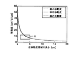
図2は、所定の長さLを有する活性領域(図1参照)で、前記低移動領域R2の長さ変化(すなわち高移動度領域R1の長さに対する低移動度領域R2の長さの比率が変化すること)による活性領域全体の移動度変化(平均、最大、最小)を示すグラフである。 FIG. 2 is an active region having a predetermined length L (see FIG. 1), and the length change of the low mobility region R2 (that is, the ratio of the length of the low mobility region R2 to the length of the high mobility region R1). It is a graph which shows the mobility change (average, maximum, minimum) of the whole active region by change.
図2に示すように、低移動度領域R2の長さが増加するほど移動度の変化が緩やかになり、特に移動度の偏差が低下する。例えば、x=0である場合、すなわち低移動度領域R2を設けずにpoly−Si(高移動度領域R1)のみにより活性領域が設けられた場合の移動度は、約50cm2/Vsであり、その偏差は20%に達する。図2において、中央の曲線(実線)は平均移動度、上部の曲線(破線)は最大移動度、そして、下部の曲線(一点鎖線)は最小移動度の変化を示す。低移動度領域R2の長さxが0から3μmへと増加していくにつれて、移動度は急減するが、xの値が3〜5μmでは移動度の変化は緩やかになる。そして、最大移動度と最小移動度との差が縮小することにより、移動度の偏差が大きく低下し、安定化する。例えば、低移動度領域R2の幅が3.1μmと算出された場合に移動度は10cm2/Vsであり、その偏差は3.6%程度に低下する。図3は、図2の四角で囲んだA部分の拡大図である。図3を参照すれば、平均、最大、最小移動度値の偏差が低移動度領域の幅の厚さ増加と共に減少することがわかる。 As shown in FIG. 2, as the length of the low mobility region R2 increases, the change in mobility becomes gradual, and in particular, the mobility deviation decreases. For example, when x = 0, that is, when the active region is provided only by poly-Si (high mobility region R1) without providing the low mobility region R2, the mobility is about 50 cm 2 / Vs. The deviation reaches 20%. In FIG. 2, the center curve (solid line) shows the change in average mobility, the upper curve (dashed line) shows the maximum mobility, and the lower curve (dashed line) shows the change in the minimum mobility. As the length x of the low mobility region R2 increases from 0 to 3 μm, the mobility decreases rapidly, but when the value of x is 3 to 5 μm, the change in mobility becomes moderate. Then, as the difference between the maximum mobility and the minimum mobility is reduced, the mobility deviation is greatly reduced and stabilized. For example, when the width of the low mobility region R2 is calculated to be 3.1 μm, the mobility is 10 cm 2 / Vs, and the deviation is reduced to about 3.6%. FIG. 3 is an enlarged view of a portion A surrounded by a square in FIG. Referring to FIG. 3, it can be seen that the deviation of the average, maximum and minimum mobility values decreases with increasing width thickness of the low mobility region.
前記のように、poly−Siは、100cm2/Vsという非常に高い移動度を示す。これは、現在までに開発されているあらゆる種類の半導体素子に十分に適用できるレベルの移動度である。換言すれば、Poly−Siの移動度は、本発明の一実施形態として前述したように、一定レベル以下に低下させても、既存の半導体素子に十分に適用できる程度の移動度を有する。例えば、5〜30cm2/Vs程度の移動度を要求するOLEDの場合、移動度が30cm2/Vs程度まで低下しても製品の品質に全く問題がない。このような点を考慮して、本発明は、移動度を半導体素子の性能に影響を与えないレベルまでに下げ、このように移動度を低下させることにより移動度の偏差を抑えることによって、同時に製造される複数の半導体素子の移動度の均一性を高めることができる。このように移動度を適切に低下させるために、本実施形態では、高移動度領域R1をp−Siで形成し、部分的に、移動度の低い物質(例えば、a−Si)で低移動度領域R2を設ける。 As described above, poly-Si exhibits a very high mobility of 100 cm 2 / Vs. This is a level of mobility that can be applied to all types of semiconductor devices that have been developed to date. In other words, the mobility of Poly-Si has such a mobility that it can be sufficiently applied to existing semiconductor elements even if it is lowered to a certain level or less as described above as one embodiment of the present invention. For example, in the case of an OLED requiring the mobility of about 5 to 30 cm 2 / Vs, there is no any problem of product quality even when reduced to about 30 cm 2 / Vs mobility. In view of such points, the present invention reduces the mobility to a level that does not affect the performance of the semiconductor element, and thus reduces the mobility, thereby reducing the mobility deviation. The uniformity of mobility of a plurality of manufactured semiconductor elements can be improved. In order to appropriately reduce the mobility as described above, in the present embodiment, the high mobility region R1 is formed of p-Si, and the mobility is partially reduced by a substance having low mobility (for example, a-Si). A degree region R2 is provided.
図4は、本発明の一実施形態に係る活性領域(図1参照)を有する半導体素子製造時の移動度の偏差の変化を示すグラフである。図4では、高移動度領域R1の移動度が40〜60cm2/Vsであり、低移動度領域R2の移動度が約0.5cm2/Vsであるときの、低移動度領域R2の長さ変化に対する移動度の偏差が示されている。図4に示すグラフから、低移動度領域R2の長さが増加するほど移動度の偏差が低下し、特に、低移動度領域R2の長さが0〜3μmの範囲で急低下し、3〜5μm以上では移動度の変化が安定化することがわかる。 FIG. 4 is a graph showing a change in mobility deviation when manufacturing a semiconductor device having an active region (see FIG. 1) according to an embodiment of the present invention. In FIG. 4, the length of the low mobility region R2 when the mobility of the high mobility region R1 is 40-60 cm 2 / Vs and the mobility of the low mobility region R2 is about 0.5 cm 2 / Vs. The deviation of the mobility with respect to the change in height is shown. From the graph shown in FIG. 4, the mobility deviation decreases as the length of the low mobility region R2 increases. In particular, the length of the low mobility region R2 rapidly decreases in the range of 0 to 3 μm. It can be seen that the change in mobility is stabilized at 5 μm or more.
従って、本発明に係る半導体素子は、電子が移動する経路上に大部分の領域を占める高移動度領域を設け、高移動度領域のたとえば中間に部分的に低移動度領域を設けて電子の移動度を引き下げる。このような高移動領域および低移動度領域は、図1に示し、上述した形態とは異なる多様な形態の実施例に変更することができる。 Therefore, the semiconductor device according to the present invention provides a high mobility region that occupies most of the region on the path along which electrons move, and provides a low mobility region partially in the middle of the high mobility region. Reduce mobility. Such a high mobility region and a low mobility region can be changed to various forms of embodiments different from the form shown in FIG. 1 and described above.
図5(a)に示す実施例では、本発明に係る半導体素子の活性領域は、複数の高移動度領域R1と複数の低移動度領域R2とが交互に配置される構造を有する。 In the embodiment shown in FIG. 5A, the active region of the semiconductor device according to the present invention has a structure in which a plurality of high mobility regions R1 and a plurality of low mobility regions R2 are alternately arranged.
図5(b)に示す実施例では、本発明に係る半導体素子の活性領域は、長さの異なる二つの高移動度領域R1、R1の間に低移動度領域R2が配置されている。 In the embodiment shown in FIG. 5B, in the active region of the semiconductor device according to the present invention, a low mobility region R2 is arranged between two high mobility regions R1 and R1 having different lengths.
図5(c)に示す実施例では、本発明に係る半導体素子の活性領域は、一つの高移動度領域R1の一端に一つの低移動度領域R2が設けられている。 In the embodiment shown in FIG. 5C, the active region of the semiconductor device according to the present invention is provided with one low mobility region R2 at one end of one high mobility region R1.
図5(d)に示す実施例によれば、本発明に係る半導体素子の活性領域は、二つの高移動度領域R1の間に一つの低移動度領域R2が傾斜して配置されている。 According to the embodiment shown in FIG. 5D, in the active region of the semiconductor device according to the present invention, one low mobility region R2 is disposed between two high mobility regions R1 so as to be inclined.
図6は、本発明の概念に基づいたものであって、図1および図5(a)ないし5(d)に示し、説明した実施形態とは異なる配置構造を有する実施例を示す。図6を参照すれば、高移動度の物質、例えば、マイクロpoly−Si(poly−Siに比べて小粒径の結晶性Si、以下、μ−Si)またはpoly−Siによって全体活性領域が定義され、この高移動度領域R1内に低移動度の物質、例えば、a−Siまたはμ−Siからなる低移動度領域R2が島状に配置されている。これは、電子が高移動度の物質層を通過しながら必ず低移動度の物質層を経由するようにするためのものである。 FIG. 6 is based on the concept of the present invention, and shows an example having an arrangement structure different from the embodiment shown in FIGS. 1 and 5A to 5D and described. Referring to FIG. 6, the entire active region is defined by a high mobility material, for example, micro poly-Si (crystalline Si having a smaller particle size than poly-Si, hereinafter μ-Si) or poly-Si . In the high mobility region R1 , a low mobility region R2 made of a material having a low mobility, for example, a-Si or μ-Si , is arranged in an island shape. This is to ensure that electrons pass through the low mobility material layer while passing through the high mobility material layer.
ここで、低移動度物質および高移動度物質は、相対的な移動度差によって選択される。例えば、低移動度物質がa−Siである場合には、これより高い移動度の物質、例えば、μ−Si、poly−Siのどちらかを、孔移動度物質として選択することができる。そして、低移動度物質がμ−Siである場合には、高移動度物質として、例えば、poly−Siを選択することができる。また、低移動度物質が単結晶Siである場合には、例えば、SiGeを高移動度物質として選択することができる。ここで言及されていない物質であっても、活性層として使用可能なすべての物質が選択可能であり、あらゆる組み合わせの物質により活性層を形成した半導体素子と、これを適用するいかなる装置が、本発明の技術的範囲に属するものと理解される。 Here, the low mobility material and the high mobility material are selected according to a relative mobility difference. For example, when the low mobility substance is a-Si, a substance having a higher mobility, for example, μ-Si or poly-Si can be selected as the pore mobility substance. When the low mobility material is μ-Si, for example, poly-Si can be selected as the high mobility material. When the low mobility material is single crystal Si, for example, SiGe can be selected as the high mobility material. All materials that can be used as the active layer can be selected even if they are not mentioned here, and any semiconductor device in which the active layer is formed of any combination of materials and any device to which this device is applied can be used. It is understood that it belongs to the technical scope of the invention.
前記のような構造を有する活性層は、多様な方法により得ることができる。 The active layer having the above structure can be obtained by various methods.
図7A〜図7Cを参照して、本発明に係る半導体素子の活性領域の製造方法の一例を説明する。まず、図7Aに示すように、SiO2が形成されたSi基板(Si-Sub)上に、PE−CVD(Plasma Enhanced-Chemical Vapor Deposition)または低圧CVD(Low Pressure CVD:LPCVD)により、a−Siを蒸着する。 An example of a method for manufacturing an active region of a semiconductor device according to the present invention will be described with reference to FIGS. 7A to 7C. First, as shown in FIG. 7A, on a Si substrate on which SiO 2 is formed (Si-Sub), PE-CVD (Plasma Enhanced-Chemical Vapor Deposition) or low-pressure CVD (Low Pressure CVD: LPCVD) is performed. Si is deposited.
次に、図7Bに示すように、低移動度領域として定義した所定の領域をマスクMで覆った後にエキシマーレーザーを照射して露出した部分を結晶化させてPoly−Siを形成する。このような選択的ELA(Excimer Laser Annealing)により、図7Cに示すような、poly−Siにより形成された高移動度領域とa−Siにより形成された低移動度領域とを有する活性層を得る。 Next, as shown in FIG. 7B, a predetermined region defined as a low mobility region is covered with a mask M, and then the exposed portion is irradiated with an excimer laser to crystallize to form Poly-Si. By such selective ELA (Excimer Laser Annealing), an active layer having a high mobility region formed by poly-Si and a low mobility region formed by a-Si as shown in FIG. 7C is obtained. .
図8A〜図8Cを参照して、本発明に係る半導体素子の活性領域の製造方法の他の例を説明する。まず、図8Aに示すように、SiO2が形成されたSi基板上に、CAT−CVD(Catalytic-Chemical Vapor Deposition)、ICP−CVD(Inductively Coupled Plasma-Chemical Vapor Deposition)、UHV−CVD(Ultra-High Vacuum-Chemical Vapor Deposition)により、μ−Siを蒸着する。 With reference to FIGS. 8A to 8C, another example of a method for manufacturing an active region of a semiconductor device according to the present invention will be described. First, as shown in FIG. 8A, on a Si substrate on which SiO 2 is formed, CAT-CVD (Catalytic-Chemical Vapor Deposition), ICP-CVD (Inductively Coupled Plasma-Chemical Vapor Deposition), UHV-CVD (Ultra-CVD) Μ-Si is deposited by High Vacuum-Chemical Vapor Deposition.
次に、図8Bに示すように、低移動度領域として定義した所定の領域をマスクMで覆った後にエキシマーレーザーを照射して露出したμ−Siの部分を再結晶化させる。このようなマスクによる選択的ELAにより、図8Cに示すような、poly−Siにより形成された高移動度領域とμ−Siにより形成された低移動度領域とを有する活性領域を得る。 Next, as shown in FIG. 8B, a predetermined region defined as a low mobility region is covered with a mask M, and then exposed to excimer laser to recrystallize the exposed portion of μ-Si. By selective ELA using such a mask, an active region having a high mobility region formed of poly-Si and a low mobility region formed of μ-Si as shown in FIG. 8C is obtained.
図7Aないし図7Cおよび図8Aないし図8Cは、活性領域に低移動度領域と高移動度領域とを形成する過程は、例えば、TFTまたはこれを有するディスプレイ素子の製造過程中に行われる。各工程は、目的の半導体素子の所望の属性に合わせて、適宜変更可能である。 7A to 7C and FIGS. 8A to 8C, the process of forming the low mobility region and the high mobility region in the active region is performed, for example, during the manufacturing process of the TFT or the display device having the TFT. Each process can be appropriately changed in accordance with a desired attribute of the target semiconductor element.
前記のような工程は、ウェーハ単位で行わる。すなわち、ウェーハは、周知のようにX−Yステージ上に搭載され、一回の工程によって前記のような活性領域を有する複数のチャンネルが同時に形成される。 The above process is performed on a wafer basis. That is, the wafer is mounted on an XY stage as is well known, and a plurality of channels having the active region as described above are simultaneously formed by a single process.
図9は、本発明に係るTFTの概略的な断面図である。図9を参照すれば、SiO2絶縁膜11が形成された基板10の上面に、シリコンフィルム層20が形成されている。シリコンフィルム層20上には、シリコンフィルム層20の両端部に対応するコンタクトホール31、32を有するゲート絶縁層30が形成されている。このゲート絶縁層30上の前記コンタクトホール31、32の間の中央部分にゲート40が形成されており、その上にIMD(intermetallic dielectric)層50が形成されている。このIMD層50には前記コンタクトホール31、32に一致する位置にコンタクトホール51、52がそれぞれ形成されている。前記IMD層50でコンタクトホール51、52上にはソース電極61およびドレイン電極62が形成されてその下部のシリコンフィルム層20の両端にそれぞれ電気的に接触している。
FIG. 9 is a schematic cross-sectional view of a TFT according to the present invention. Referring to FIG. 9, a
前記シリコンフィルム層20で前記ソース電極61およびドレイン電極62が接触する部分は、高伝導性を有するドーピング領域であり、これら間の領域は、ゲート40により電界効果が発生する活性領域である。この活性領域は、前述したような高移動度領域R1と低移動度領域R2とを有する。図9に示した活性領域は、図1と同様の形態で高移動度領域R1および低移動度領域R2が配置された構造を有する。
A portion where the source electrode 61 and the drain electrode 62 are in contact with each other in the
前記のような活性領域は、図5および図6に示すような形態を有するものとすることができる。前記活性領域は、その両側のドーピングされた領域、すなわち、ソースおよびドレインとともに一つのSiフィルム層から得られる。周知のように、ソースおよびドレインは高濃度にドーピングされた領域である。これらの間の活性領域は、高移動度を有するように選択的に結晶化されるか、局部的に移動度を変えるように差別的に結晶化された領域である。このような選択的結晶化または差別的結晶化は前述したので、その詳細な説明は省略する。 The active region as described above may have a form as shown in FIGS. The active region is obtained from one Si film layer with doped regions on both sides, ie, source and drain. As is well known, the source and drain are heavily doped regions. The active region between them is a region that is selectively crystallized so as to have high mobility, or that is differentially crystallized so as to locally change mobility. Since such selective crystallization or differential crystallization has been described above, a detailed description thereof will be omitted.
このようなTFTは、半導体メモリ素子、平板ディスプレイ素子などの分野に幅広く使用される。前述した基板は、ガラスまたはプラスチックにより形成することができる。プラスチックを基板として使用する素子には、平板(フラットパネル)ディスプレイ素子、特にOLED(Organic Light-Emitting Diode)が挙げられる。すなわち、本発明はOLEDに好適である。 Such TFTs are widely used in fields such as semiconductor memory devices and flat panel display devices. The aforementioned substrate can be formed of glass or plastic. An element using plastic as a substrate includes a flat panel display element, particularly an OLED (Organic Light-Emitting Diode). That is, the present invention is suitable for OLED.
前述したTFTは、いわゆるトップゲート型である。しかし、前記のような構造の活性領域を有する限り、ボトムゲート型にも適用可能であり、前述の内容に基づいて容易に実現可能である。 The above-described TFT is a so-called top gate type. However, as long as the active region having the structure as described above is provided, it can be applied to a bottom gate type and can be easily realized based on the above-described contents.
以上、本発明の理解のために、いくつかの望ましい実施形態を説明し、添付図面に示したが、これらの実施形態は、単に発明を例示するものに過ぎず、これを制限するものではない。また、本発明は、図示され、説明された構造と配列に限定されるものではなく、当業者によって多様な修正が可能である。 For the purpose of understanding the present invention, several preferred embodiments have been described and illustrated in the accompanying drawings, which are merely illustrative of the invention and are not limiting. . Further, the present invention is not limited to the structure and arrangement shown and described, and various modifications can be made by those skilled in the art.
本発明は、シリコンを基盤とする半導体素子、特に電界によりチャンネルを形成する活性層を有するすべての素子に適用可能である。最も広く応用が期待される分野はTFTであって、代表的なターゲット製品はフラットパネルディスプレイ素子である。 The present invention is applicable to silicon-based semiconductor devices, particularly all devices having an active layer that forms a channel by an electric field. The field where application is expected most widely is TFT, and a typical target product is a flat panel display element.
R1 高移動度領域
R2 低移動度領域
R1 High mobility region R2 Low mobility region
Claims (4)
前記チャンネルの両側に設けられるソースおよびドレインと、
前記チャンネルに電界を印加するゲートと、
前記チャンネルとゲートとの間に介在する絶縁層と、を備え、
前記チャンネルは、電子移動経路上に高移動度領域と低移動度領域とを含む構造を有し、
前記低移動度領域が、前記高移動度領域内に島状に配置されている、
ことを特徴とする薄膜トランジスタ。 Silicon-based channels,
A source and a drain provided on both sides of the channel;
A gate for applying an electric field to the channel;
An insulating layer interposed between the channel and the gate,
The channel is to have a structure including a high mobility area and the low mobility area on electron transfer path,
The low mobility region is arranged in an island shape in the high mobility region,
A thin film transistor.
前記低移動度領域は非晶質構造を有することを特徴とする請求項1に記載の薄膜トランジスタ。 The high mobility region has a polycrystalline structure;
2. The thin film transistor according to claim 1 , wherein the low mobility region has an amorphous structure.
前記低移動度領域はマイクロ多結晶構造を有することを特徴とする請求項1に記載の薄膜トランジスタ。 The high mobility region has a polycrystalline structure;
The thin film transistor according to claim 1 , wherein the low mobility region has a micropolycrystalline structure.
前記低移動度領域は単結晶構造を有することを特徴とする請求項1に記載の薄膜トランジスタ。 The high mobility region has a SiGe crystal structure;
The thin film transistor according to claim 1 , wherein the low mobility region has a single crystal structure.
Applications Claiming Priority (2)
| Application Number | Priority Date | Filing Date | Title |
|---|---|---|---|
| KR1020030100494A KR100975523B1 (en) | 2003-12-30 | 2003-12-30 | Semiconductor device with modified mobility and thin film transistor having the same |
| KR2003-100494 | 2003-12-30 |
Publications (2)
| Publication Number | Publication Date |
|---|---|
| JP2005197719A JP2005197719A (en) | 2005-07-21 |
| JP5069842B2 true JP5069842B2 (en) | 2012-11-07 |
Family
ID=34567859
Family Applications (1)
| Application Number | Title | Priority Date | Filing Date |
|---|---|---|---|
| JP2004379166A Expired - Fee Related JP5069842B2 (en) | 2003-12-30 | 2004-12-28 | Thin film transistor |
Country Status (4)
| Country | Link |
|---|---|
| US (1) | US7479667B2 (en) |
| EP (1) | EP1551059A3 (en) |
| JP (1) | JP5069842B2 (en) |
| KR (1) | KR100975523B1 (en) |
Families Citing this family (11)
| Publication number | Priority date | Publication date | Assignee | Title |
|---|---|---|---|---|
| JP4560505B2 (en) | 2005-11-08 | 2010-10-13 | キヤノン株式会社 | Field effect transistor |
| JP4169071B2 (en) | 2006-05-25 | 2008-10-22 | ソニー株式会社 | Display device |
| JP5398910B2 (en) * | 2010-05-12 | 2014-01-29 | 帝人株式会社 | ORGANIC SEMICONDUCTOR FILM, ITS MANUFACTURING METHOD, AND CONTACT PRINT STAMP |
| US10243003B2 (en) * | 2015-03-27 | 2019-03-26 | Sakai Display Products Corporation | Thin film transistor and display panel |
| JPWO2016157351A1 (en) * | 2015-03-30 | 2018-01-18 | 堺ディスプレイプロダクト株式会社 | Thin film transistor and display panel |
| CN109075043A (en) * | 2016-03-04 | 2018-12-21 | 堺显示器制品株式会社 | Laser anneal device, exposure mask, thin film transistor (TFT) and laser anneal method |
| CN105789327B (en) * | 2016-05-17 | 2019-05-03 | 京东方科技集团股份有限公司 | A kind of thin film transistor (TFT) and preparation method thereof, array substrate, display device |
| CN107482065A (en) * | 2017-09-15 | 2017-12-15 | 京东方科技集团股份有限公司 | A kind of thin film transistor (TFT) preparation method, thin film transistor (TFT) and backboard, display device |
| CN107482066B (en) * | 2017-09-20 | 2021-01-15 | 京东方科技集团股份有限公司 | Thin film transistor, preparation method thereof, array substrate and display device |
| CN109742024B (en) * | 2019-01-02 | 2021-01-26 | 京东方科技集团股份有限公司 | Laser annealing method and array substrate |
| CN110972508B (en) * | 2019-03-04 | 2022-05-03 | 京东方科技集团股份有限公司 | Thin film transistor and method for manufacturing thin film transistor |
Family Cites Families (19)
| Publication number | Priority date | Publication date | Assignee | Title |
|---|---|---|---|---|
| JP3173854B2 (en) * | 1992-03-25 | 2001-06-04 | 株式会社半導体エネルギー研究所 | Method for manufacturing thin-film insulated gate semiconductor device and semiconductor device manufactured |
| US5461250A (en) * | 1992-08-10 | 1995-10-24 | International Business Machines Corporation | SiGe thin film or SOI MOSFET and method for making the same |
| JPH0786604A (en) * | 1993-09-17 | 1995-03-31 | Mitsubishi Electric Corp | Thin-film transistor and manufacture thereof |
| JPH08195495A (en) * | 1994-05-31 | 1996-07-30 | Sanyo Electric Co Ltd | Semiconductor device, manufacture of semiconductor device, film transistor, manufacture of film transistor, and display |
| EP0801427A3 (en) * | 1996-04-11 | 1999-05-06 | Matsushita Electric Industrial Co., Ltd. | Field effect transistor, semiconductor storage device, method of manufacturing the same and method of driving semiconductor storage device |
| JP3204986B2 (en) | 1996-05-28 | 2001-09-04 | ザ トラスティース オブ コロンビア ユニヴァーシティ イン ザ シティ オブ ニューヨーク | Crystallization of semiconductor film region on substrate and device manufactured by this method |
| US5981974A (en) * | 1996-09-30 | 1999-11-09 | Sharp Kabushiki Kaisha | Semiconductor device and method for fabricating the same |
| JP3357798B2 (en) * | 1996-09-30 | 2002-12-16 | シャープ株式会社 | Semiconductor device and method of manufacturing the same |
| JP4024954B2 (en) * | 1998-02-06 | 2007-12-19 | 株式会社東芝 | Semiconductor device and manufacturing method thereof |
| JP4436469B2 (en) * | 1998-09-30 | 2010-03-24 | 三洋電機株式会社 | Semiconductor device |
| GB9927287D0 (en) * | 1999-11-19 | 2000-01-12 | Koninkl Philips Electronics Nv | Top gate thin film transistor and method of producing the same |
| JP3927756B2 (en) * | 2000-05-16 | 2007-06-13 | シャープ株式会社 | Manufacturing method of semiconductor device |
| WO2002009192A1 (en) * | 2000-07-24 | 2002-01-31 | Matsushita Electric Industrial Co., Ltd. | Semiconductor device, liquid crystal display device, el display device, semiconductor film producing method, and semiconductor device producing method |
| JP4045731B2 (en) * | 2000-09-25 | 2008-02-13 | 株式会社日立製作所 | Thin film semiconductor device manufacturing method |
| KR100409233B1 (en) * | 2000-10-31 | 2003-12-18 | 재단법인서울대학교산학협력재단 | Method of Manufacturing Polycrystalline Silicon Thin Film Transistor using Excimer Laser annealing |
| JP4358998B2 (en) * | 2001-02-01 | 2009-11-04 | 株式会社日立製作所 | Thin film transistor device and manufacturing method thereof |
| JP2002314092A (en) * | 2001-02-09 | 2002-10-25 | Semiconductor Energy Lab Co Ltd | Semiconductor device and manufacturing method therefor |
| US7141822B2 (en) * | 2001-02-09 | 2006-11-28 | Semiconductor Energy Laboratory Co., Ltd. | Semiconductor device and method for manufacturing the same |
| US7164152B2 (en) * | 2003-09-16 | 2007-01-16 | The Trustees Of Columbia University In The City Of New York | Laser-irradiated thin films having variable thickness |
-
2003
- 2003-12-30 KR KR1020030100494A patent/KR100975523B1/en not_active IP Right Cessation
-
2004
- 2004-12-20 EP EP04257956A patent/EP1551059A3/en not_active Ceased
- 2004-12-28 US US11/022,756 patent/US7479667B2/en not_active Expired - Fee Related
- 2004-12-28 JP JP2004379166A patent/JP5069842B2/en not_active Expired - Fee Related
Also Published As
| Publication number | Publication date |
|---|---|
| KR20050070675A (en) | 2005-07-07 |
| US20050139923A1 (en) | 2005-06-30 |
| EP1551059A3 (en) | 2006-10-18 |
| EP1551059A2 (en) | 2005-07-06 |
| KR100975523B1 (en) | 2010-08-13 |
| US7479667B2 (en) | 2009-01-20 |
| JP2005197719A (en) | 2005-07-21 |
Similar Documents
| Publication | Publication Date | Title |
|---|---|---|
| US6479838B2 (en) | Thin film transistor, thin film transistor array substrate, liquid crystal display device, and electroluminescent display device | |
| KR100682892B1 (en) | The fabrication method of thin film transistor | |
| US20070128777A1 (en) | POLY-Si THIN FILM TRANSISTOR AND ORGANIC LIGHT-EMITTING DISPLAY HAVING THE SAME | |
| US7344930B2 (en) | Semiconductor device and manufacturing method thereof | |
| JP5820402B2 (en) | THIN FILM TRANSISTOR DEVICE AND METHOD FOR MANUFACTURING THIN FILM TRANSISTOR DEVICE | |
| US20060199317A1 (en) | Thin film transistor and method for production thereof | |
| JP5069842B2 (en) | Thin film transistor | |
| KR20100034634A (en) | Thin film transistor and manufacturing method of the same | |
| JP2007158290A (en) | Organic light emitting diode (oled) display panel, and method of forming polysilicon channel layer thereof | |
| JP2007221120A (en) | Organic light-emitting device and method of manufacturing the same | |
| US7229860B2 (en) | Method for manufacturing a thin film transistor using poly silicon | |
| JP2009194362A (en) | Thin-film transistor containing nanowire, and its manufacturing method | |
| JPH10270701A (en) | Thin film transistor and its production | |
| KR100319206B1 (en) | Method for fabricating a thin film transistor and a substrate, thin film transistor fabricated the same | |
| US20050224876A1 (en) | [structure of ltps-tft and method of fabricating channel layer thereof] | |
| US20060172469A1 (en) | Method of fabricating a polycrystalline silicon thin film transistor | |
| JP4338488B2 (en) | Design method of TFT using dual or multiple gate | |
| JP2002185005A (en) | Hybrid tft array substrate and its manufacturing method | |
| US7115449B2 (en) | Method for fabrication of polycrystalline silicon thin film transistors | |
| KR100534577B1 (en) | Display device having good performance | |
| JP2004200648A (en) | Thin-film transistor having ldd/offset structure | |
| KR100751315B1 (en) | Thin film transistor, method of the TFT, and flat panel display device with the TFT | |
| KR20040043729A (en) | Thin film transistor and electorluminescent display device using thereof | |
| KR20100055194A (en) | Thin film transistor and manufacturing method thereof | |
| US7014708B2 (en) | Method of forming a thin film transistor by utilizing a laser crystallization process |
Legal Events
| Date | Code | Title | Description |
|---|---|---|---|
| A621 | Written request for application examination |
Free format text: JAPANESE INTERMEDIATE CODE: A621 Effective date: 20071113 |
|
| A977 | Report on retrieval |
Free format text: JAPANESE INTERMEDIATE CODE: A971007 Effective date: 20110623 |
|
| A131 | Notification of reasons for refusal |
Free format text: JAPANESE INTERMEDIATE CODE: A131 Effective date: 20110628 |
|
| A521 | Request for written amendment filed |
Free format text: JAPANESE INTERMEDIATE CODE: A523 Effective date: 20110927 |
|
| A131 | Notification of reasons for refusal |
Free format text: JAPANESE INTERMEDIATE CODE: A131 Effective date: 20111108 |
|
| TRDD | Decision of grant or rejection written | ||
| A01 | Written decision to grant a patent or to grant a registration (utility model) |
Free format text: JAPANESE INTERMEDIATE CODE: A01 Effective date: 20120807 |
|
| A01 | Written decision to grant a patent or to grant a registration (utility model) |
Free format text: JAPANESE INTERMEDIATE CODE: A01 |
|
| A61 | First payment of annual fees (during grant procedure) |
Free format text: JAPANESE INTERMEDIATE CODE: A61 Effective date: 20120820 |
|
| FPAY | Renewal fee payment (event date is renewal date of database) |
Free format text: PAYMENT UNTIL: 20150824 Year of fee payment: 3 |
|
| R150 | Certificate of patent or registration of utility model |
Free format text: JAPANESE INTERMEDIATE CODE: R150 |
|
| LAPS | Cancellation because of no payment of annual fees |