JP5066326B2 - Apparatus and method for producing an electronic component having at least one active organic layer - Google Patents
Apparatus and method for producing an electronic component having at least one active organic layer Download PDFInfo
- Publication number
- JP5066326B2 JP5066326B2 JP2005142201A JP2005142201A JP5066326B2 JP 5066326 B2 JP5066326 B2 JP 5066326B2 JP 2005142201 A JP2005142201 A JP 2005142201A JP 2005142201 A JP2005142201 A JP 2005142201A JP 5066326 B2 JP5066326 B2 JP 5066326B2
- Authority
- JP
- Japan
- Prior art keywords
- layer
- sacrificial layer
- organic
- substrate
- component
- Prior art date
- Legal status (The legal status is an assumption and is not a legal conclusion. Google has not performed a legal analysis and makes no representation as to the accuracy of the status listed.)
- Active
Links
- 238000004519 manufacturing process Methods 0.000 title claims description 21
- 239000012044 organic layer Substances 0.000 title description 4
- 238000000034 method Methods 0.000 claims description 41
- 239000004065 semiconductor Substances 0.000 claims description 27
- 239000000758 substrate Substances 0.000 claims description 18
- 238000004804 winding Methods 0.000 claims description 13
- 239000000463 material Substances 0.000 claims description 12
- 239000004020 conductor Substances 0.000 claims description 9
- 239000010410 layer Substances 0.000 description 80
- 229910052751 metal Inorganic materials 0.000 description 11
- 239000002184 metal Substances 0.000 description 10
- 238000007639 printing Methods 0.000 description 10
- 238000001459 lithography Methods 0.000 description 7
- 239000011248 coating agent Substances 0.000 description 6
- 238000000576 coating method Methods 0.000 description 6
- 238000000151 deposition Methods 0.000 description 6
- 239000002904 solvent Substances 0.000 description 6
- 230000008021 deposition Effects 0.000 description 5
- 238000010276 construction Methods 0.000 description 4
- 238000004544 sputter deposition Methods 0.000 description 4
- 229910018072 Al 2 O 3 Inorganic materials 0.000 description 3
- 230000004888 barrier function Effects 0.000 description 3
- 239000003921 oil Substances 0.000 description 3
- 229920002120 photoresistant polymer Polymers 0.000 description 3
- XMWRBQBLMFGWIX-UHFFFAOYSA-N C60 fullerene Chemical compound C12=C3C(C4=C56)=C7C8=C5C5=C9C%10=C6C6=C4C1=C1C4=C6C6=C%10C%10=C9C9=C%11C5=C8C5=C8C7=C3C3=C7C2=C1C1=C2C4=C6C4=C%10C6=C9C9=C%11C5=C5C8=C3C3=C7C1=C1C2=C4C6=C2C9=C5C3=C12 XMWRBQBLMFGWIX-UHFFFAOYSA-N 0.000 description 2
- 229910052782 aluminium Inorganic materials 0.000 description 2
- XAGFODPZIPBFFR-UHFFFAOYSA-N aluminium Chemical compound [Al] XAGFODPZIPBFFR-UHFFFAOYSA-N 0.000 description 2
- 238000011437 continuous method Methods 0.000 description 2
- 238000004090 dissolution Methods 0.000 description 2
- 239000011888 foil Substances 0.000 description 2
- 229910003472 fullerene Inorganic materials 0.000 description 2
- 238000010438 heat treatment Methods 0.000 description 2
- 239000000203 mixture Substances 0.000 description 2
- 229920000123 polythiophene Polymers 0.000 description 2
- 239000011241 protective layer Substances 0.000 description 2
- 239000010409 thin film Substances 0.000 description 2
- OYPRJOBELJOOCE-UHFFFAOYSA-N Calcium Chemical compound [Ca] OYPRJOBELJOOCE-UHFFFAOYSA-N 0.000 description 1
- 206010034972 Photosensitivity reaction Diseases 0.000 description 1
- 229910004541 SiN Inorganic materials 0.000 description 1
- 229910004298 SiO 2 Inorganic materials 0.000 description 1
- 229910052791 calcium Inorganic materials 0.000 description 1
- 239000011575 calcium Substances 0.000 description 1
- 239000000919 ceramic Substances 0.000 description 1
- 238000010924 continuous production Methods 0.000 description 1
- 238000007796 conventional method Methods 0.000 description 1
- 239000007772 electrode material Substances 0.000 description 1
- 230000008020 evaporation Effects 0.000 description 1
- 238000001704 evaporation Methods 0.000 description 1
- 230000012447 hatching Effects 0.000 description 1
- AMGQUBHHOARCQH-UHFFFAOYSA-N indium;oxotin Chemical compound [In].[Sn]=O AMGQUBHHOARCQH-UHFFFAOYSA-N 0.000 description 1
- 238000010297 mechanical methods and process Methods 0.000 description 1
- 230000005226 mechanical processes and functions Effects 0.000 description 1
- 239000007769 metal material Substances 0.000 description 1
- 239000002105 nanoparticle Substances 0.000 description 1
- 239000012811 non-conductive material Substances 0.000 description 1
- 239000011368 organic material Substances 0.000 description 1
- 238000013086 organic photovoltaic Methods 0.000 description 1
- 239000002245 particle Substances 0.000 description 1
- 230000036211 photosensitivity Effects 0.000 description 1
- 229920000052 poly(p-xylylene) Polymers 0.000 description 1
- 229920006254 polymer film Polymers 0.000 description 1
- 238000004528 spin coating Methods 0.000 description 1
- 239000000725 suspension Substances 0.000 description 1
- 238000007740 vapor deposition Methods 0.000 description 1
- 239000001993 wax Substances 0.000 description 1
Images


Classifications
-
- H—ELECTRICITY
- H10—SEMICONDUCTOR DEVICES; ELECTRIC SOLID-STATE DEVICES NOT OTHERWISE PROVIDED FOR
- H10K—ORGANIC ELECTRIC SOLID-STATE DEVICES
- H10K71/00—Manufacture or treatment specially adapted for the organic devices covered by this subclass
-
- H—ELECTRICITY
- H10—SEMICONDUCTOR DEVICES; ELECTRIC SOLID-STATE DEVICES NOT OTHERWISE PROVIDED FOR
- H10K—ORGANIC ELECTRIC SOLID-STATE DEVICES
- H10K39/00—Integrated devices, or assemblies of multiple devices, comprising at least one organic radiation-sensitive element covered by group H10K30/00
- H10K39/10—Organic photovoltaic [PV] modules; Arrays of single organic PV cells
-
- H—ELECTRICITY
- H10—SEMICONDUCTOR DEVICES; ELECTRIC SOLID-STATE DEVICES NOT OTHERWISE PROVIDED FOR
- H10K—ORGANIC ELECTRIC SOLID-STATE DEVICES
- H10K71/00—Manufacture or treatment specially adapted for the organic devices covered by this subclass
- H10K71/10—Deposition of organic active material
- H10K71/12—Deposition of organic active material using liquid deposition, e.g. spin coating
- H10K71/13—Deposition of organic active material using liquid deposition, e.g. spin coating using printing techniques, e.g. ink-jet printing or screen printing
-
- H—ELECTRICITY
- H10—SEMICONDUCTOR DEVICES; ELECTRIC SOLID-STATE DEVICES NOT OTHERWISE PROVIDED FOR
- H10K—ORGANIC ELECTRIC SOLID-STATE DEVICES
- H10K71/00—Manufacture or treatment specially adapted for the organic devices covered by this subclass
- H10K71/20—Changing the shape of the active layer in the devices, e.g. patterning
- H10K71/221—Changing the shape of the active layer in the devices, e.g. patterning by lift-off techniques
-
- H—ELECTRICITY
- H10—SEMICONDUCTOR DEVICES; ELECTRIC SOLID-STATE DEVICES NOT OTHERWISE PROVIDED FOR
- H10K—ORGANIC ELECTRIC SOLID-STATE DEVICES
- H10K59/00—Integrated devices, or assemblies of multiple devices, comprising at least one organic light-emitting element covered by group H10K50/00
- H10K59/80—Constructional details
- H10K59/86—Series electrical configurations of multiple OLEDs
-
- Y—GENERAL TAGGING OF NEW TECHNOLOGICAL DEVELOPMENTS; GENERAL TAGGING OF CROSS-SECTIONAL TECHNOLOGIES SPANNING OVER SEVERAL SECTIONS OF THE IPC; TECHNICAL SUBJECTS COVERED BY FORMER USPC CROSS-REFERENCE ART COLLECTIONS [XRACs] AND DIGESTS
- Y02—TECHNOLOGIES OR APPLICATIONS FOR MITIGATION OR ADAPTATION AGAINST CLIMATE CHANGE
- Y02E—REDUCTION OF GREENHOUSE GAS [GHG] EMISSIONS, RELATED TO ENERGY GENERATION, TRANSMISSION OR DISTRIBUTION
- Y02E10/00—Energy generation through renewable energy sources
- Y02E10/50—Photovoltaic [PV] energy
- Y02E10/549—Organic PV cells
-
- Y—GENERAL TAGGING OF NEW TECHNOLOGICAL DEVELOPMENTS; GENERAL TAGGING OF CROSS-SECTIONAL TECHNOLOGIES SPANNING OVER SEVERAL SECTIONS OF THE IPC; TECHNICAL SUBJECTS COVERED BY FORMER USPC CROSS-REFERENCE ART COLLECTIONS [XRACs] AND DIGESTS
- Y02—TECHNOLOGIES OR APPLICATIONS FOR MITIGATION OR ADAPTATION AGAINST CLIMATE CHANGE
- Y02P—CLIMATE CHANGE MITIGATION TECHNOLOGIES IN THE PRODUCTION OR PROCESSING OF GOODS
- Y02P70/00—Climate change mitigation technologies in the production process for final industrial or consumer products
- Y02P70/50—Manufacturing or production processes characterised by the final manufactured product
Description
本発明は、基板にフォイルが使用され、かつ少なくとも一つの活性有機層を有する電子構成要素を製造するための装置及び方法に関する。 The present invention relates to an apparatus and method for producing an electronic component in which a foil is used for a substrate and which has at least one active organic layer.
スパッタリング、スピンコーティング、又は印刷等の個別の方法の連続によって、一つの層の適用後に別の層が適用され、レーザ又は湿式リソグラフ等の構成技術によって構成される、少なくとも一つの活性有機層を有する電子構成要素の製造方法が公知である。 Having at least one active organic layer constructed by a construction technique such as laser or wet lithography, by applying another layer after the application of one layer, by a sequence of individual methods such as sputtering, spin coating or printing Methods for manufacturing electronic components are known.
この方法の問題は、層が個別の作業ステップにより適用かつ構成されるため、作業ステップの間で、完成した層を溶媒、及び/又は機械的損傷から常に保護しなければならないことにある。従って、公知の製造方法は大量生産に適したものでなく、個々の構成要素の層は損傷されて、品質が劣る構成要素が生産される場合が多かった。 The problem with this method is that since the layers are applied and constructed by individual work steps, the finished layer must always be protected from solvents and / or mechanical damage during the work steps. Therefore, the known manufacturing methods are not suitable for mass production, and the layers of individual components are often damaged, producing components of poor quality.
従来の方法では有機電子構成要素をZ接続することが好ましく、このような連続的な接続では、第一構成要素の頂部電極が、次なる構成要素の底部電極に対して接続される。
現在まで、Z接続された有機電子構成要素を大量生産に適した方法にて製造することは不可能であった。
In conventional methods, it is preferable to Z-connect organic electronic components, and in such a continuous connection, the top electrode of the first component is connected to the bottom electrode of the next component.
To date, it has not been possible to produce Z-connected organic electronic components in a manner suitable for mass production.
従って、本発明の目的は、大量生産に適した方法で製造することが可能な、高品質な、及び/又は、従来のZ接続を有し、有機光起電性を備えた、及び/又はエレクトロクロミックな構成要素を製造する装置及び方法を提供することにある。 The object of the present invention is therefore to have a high-quality and / or conventional Z-connection, which can be manufactured in a manner suitable for mass production, with organic photovoltaic properties, and / or It is an object of the present invention to provide an apparatus and method for manufacturing electrochromic components.
本発明は、少なくとも一つの第一巻回体と第二巻回体と、これら二つの巻回体間において三つのモジュールからなる少なくとも一つの列とを有する、光起電性を備え、及び/又はエレクトロクロミックな有機電子構成要素を製造するための装置であって、第一巻回体は未被覆基板からなる細長片からなり、第一巻回体と第二巻回体との間に配置された列内の第一モジュールによって任意で半透明の底部電極を構成し、列内の第二モジュールによって少なくとも一つの有機活性層を構成し、列内の第三モジュールによって対向電極を適用かつ構成することが可能で、第三モジュールによって被覆された可撓性を有する有機構成要素は、第三モジュールの近隣に位置する第二巻回体上に巻回され得る装置に関する。 The invention comprises a photovoltaic property comprising at least one first winding body and a second winding body, and at least one row of three modules between the two winding bodies, and / or Or an apparatus for producing an electrochromic organic electronic component, wherein the first winding body is formed of an elongated piece made of an uncoated substrate, and is arranged between the first winding body and the second winding body. The first module in the arranged row optionally constitutes a translucent bottom electrode, the second module in the row constitutes at least one organic active layer, and the third module in the row applies and constitutes the counter electrode The flexible organic component covered by the third module is related to a device that can be wound on a second winding body located in the vicinity of the third module.
本発明は、少なくとも一つの活性有機層を有する有機構成要素を、巻回体から巻回体へと連続的に製造する方法であって、少なくとも、
a)半透明の底部電極を塗布、及び/又は構成する作業ステップと、
b)有機半導体層を塗布、及び/又は構成する作業ステップと、
c)頂部対向電極を塗布、及び/又は構成する作業ステップとを含む方法も提供する。
The present invention is a method for continuously producing an organic component having at least one active organic layer from a wound body to a wound body, comprising at least:
a) applying and / or constructing a translucent bottom electrode;
b) a work step of applying and / or configuring an organic semiconductor layer;
c) a working step of applying and / or configuring the top counter electrode.
一実施形態において、一つの底部層に少なくとも一つの「犠牲層」を塗布し得る、少なくとも一つの作業ステップと一つのモジュールとを提供する。
用語「偽製層」とは、上部に配置された層と共に被覆された後、除去された際に、その除去によって別の層が損傷を受けない層を意味する。犠牲層に適した材料には、熱で除去され得る油や蝋等がある。しかしながら、「犠牲層」は、ある環境の下では、有機構成要
素上に残留するか、又は相当後の作業ステップにて除去される、フォトレジスト又は高分子薄膜の層を意味する場合もある。
In one embodiment, at least one working step and one module are provided that can apply at least one “sacrificial layer” to one bottom layer.
The term “fake layer” means a layer that, when coated with an overlying layer and then removed, does not damage another layer upon removal. Suitable materials for the sacrificial layer include oils and waxes that can be removed by heat. However, “sacrificial layer” may mean a layer of photoresist or polymer film that, under certain circumstances, remains on the organic component or is removed in a subsequent working step.
本発明の一実施形態において、半透明底部電極は、以下の方法の一つ以上を用いて塗布、及び/又は構成される。
i)シャドウマスクを介したスパッタリング
ii)湿式リソグラフィーによる構成、及び/又は、
iii)大面積適用された電極のレーザ構成、
iv)電極材料の印刷、
v)基板のスパッタリングに先立つ予備層の印刷。予備層は、次に除去されるか、又は構成要素上に残留され得る。
In one embodiment of the present invention, the translucent bottom electrode is applied and / or configured using one or more of the following methods.
i) Sputtering through a shadow mask ii) Configuration by wet lithography and / or
iii) laser configuration of electrodes applied in large areas,
iv) printing of electrode material,
v) Preliminary layer printing prior to substrate sputtering. The preliminary layer can then be removed or left on the component.
本発明の一実施形態において、有機半導体層は、以下の方法の一つ以上により塗布、及び/又は構成される。
i)半導体材料の構成的塗布(例、印刷)
ii)犠牲層(例、油)の前印刷、半導体の大面積被覆、続く犠牲層の除去。犠牲層が印刷された箇所における半導体の剥離。
iii)大面積被覆、及びその後のレーザ構成等による構成、
本発明の一実施形態において、対向電極は、以下の方法のうちの一つ以上により塗布かつ構成される。
i)湿式リソグラフィーで適切な犠牲層構造を製造(例えば有機、半導体材料等の被覆に先立ち実行され得る)、金属又は別の一つの導電性材料を大面積蒸着、UV光、加熱、及び/又は溶解等で犠牲層を除去、
ii)湿式リソグラフィー、又は印刷により、適切な非導電性構造を製造(例えば有機、半導体材料等の被覆に先立ち実行され得る)、後の金属又は別の一つの導電性材料の大面積蒸着中に蒸着層が剥離される、
iii)犠牲層構造の印刷(例えば有機、半導体材料等の被覆に先立ち実行され得る)、金属又は別の一つの導電性材料の大面積蒸着、UV光への露光、加熱、及び/又は溶解等による犠牲層の除去、
iv)非導電性材料の印刷(任意の有機半導体材料の被覆に先立ち実行され得る)、金属又は他の一つの導電性材料の大面積低角度蒸着。低角度蒸着により金属層内に断裂が発生して、レーザ誘導が排除される。
v)シャドウマスクを用いた金属又は他の一つの導電性材料のスパッタリング、又は蒸着、
vi)大面積蒸着と、続く金属又は導電性材料のレーザ構成。
In one embodiment of the present invention, the organic semiconductor layer is applied and / or configured by one or more of the following methods.
i) Constructive application of semiconductor materials (eg, printing)
ii) Preprinting of the sacrificial layer (eg oil), large area coverage of the semiconductor, followed by removal of the sacrificial layer. Stripping of the semiconductor at the location where the sacrificial layer is printed.
iii) Large area coverage and subsequent laser configuration, etc.
In one embodiment of the invention, the counter electrode is applied and configured by one or more of the following methods.
i) producing a suitable sacrificial layer structure with wet lithography (e.g. can be performed prior to coating of organic, semiconductor material, etc.), depositing metal or another conductive material on a large area, UV light, heating, and / or Removing the sacrificial layer by dissolution, etc.
ii) Manufacturing suitable non-conductive structures by wet lithography, or printing (eg, can be performed prior to coating of organic, semiconductor materials, etc.), during subsequent large area deposition of metal or another conductive material The deposited layer is peeled off,
iii) sacrificial layer structure printing (e.g. can be performed prior to coating of organic, semiconductor materials, etc.), large area deposition of metal or another conductive material, exposure to UV light, heating, and / or dissolution, etc. Sacrificial layer removal,
iv) Printing of non-conductive materials (which can be performed prior to coating of any organic semiconductor material), large area low angle deposition of metal or one other conductive material. Low angle deposition can cause tearing in the metal layer and eliminate laser guidance.
v) Sputtering or vapor deposition of metal or another conductive material using a shadow mask,
vi) Large area deposition followed by laser configuration of metal or conductive material.
一実施形態では、特に感光性材料に関連して、有機構成要素はまた封入及び/又は密閉される。
本願に説明される連続製造方法の利点は、全プロセスステップが巻回工程に適していることにある。さらに、全製造プロセス中、活性半導体層の活性領域は、溶媒及び/又は溶媒蒸気に露出されない。本発明は高品質の有機構成要素を製造し得る唯一の方法を提供する。
In one embodiment, particularly with respect to the photosensitive material, the organic component is also encapsulated and / or sealed.
The advantage of the continuous production method described in this application is that all process steps are suitable for the winding process. Furthermore, during the entire manufacturing process, the active region of the active semiconductor layer is not exposed to solvent and / or solvent vapor. The present invention provides the only method by which high quality organic components can be produced.
有機電子構成要素はフォトディテクタ、太陽電池、エレクトロクロミックな構成要素、OLEDディスプレイ、電子回路、センサ、実験室用チップ等であり得る。
以下にて、図1〜13に概略的に図示された選択的な実施例を基に、本発明を更に詳細に説明する。
Organic electronic components can be photodetectors, solar cells, electrochromic components, OLED displays, electronic circuits, sensors, laboratory chips, and the like.
In the following, the present invention will be described in more detail on the basis of an alternative embodiment schematically illustrated in FIGS.
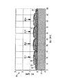
図1は、基板32上にて一連のZ接続有機構成要素を経由する電流路6を示すグラフで
ある。この断面図にて、電流路6は斜線で示される。電流路6は、構成要素30.1の底部要素31、構成要素30の半導体35及び頂部電極36、次なる構成要素30.2の底部電極31、半導体35、電極36を経由して、第三の構成要素30.3の底部電極31、更に次なる構成要素へと配線されている。グラフでは、構成要素の代表的な寸法が示されている。
FIG. 1 is a graph showing a current path 6 through a series of Z-connected organic components on a
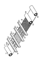
図2に、(簡略化された)巻回プロセスの連続方法の実施形態を示す。図の左上に、基板32が巻回された巻回体11が図示されている。この巻回体には、半透明の底部電極31が被覆されている。プロセスステップ2.1は第一の横断バー14の前方にて実行され、大面積上に底部電極が塗布される。プロセスステップ2.2では、半透明の底部電極31を構成する。半透明の底部電極は、ITO(インジウムスズ酸化物)電極が好ましい。プロセスステップ2.3では、半導体35を大面積上に塗布する。プロセスステップ2.4では、有機材料等から形成されている半導体35を構成する。プロセスステップ2.4の後、プロセスステップ2.5にて金属を大面積上に堆積する。図面では、薄膜35/36を介して底部層が構成される工程が比較的実際的に示されている。巻回体15によって有機構成要素を封止し、封止された構成要素は再度、細長形態にて巻回されて巻回体16が形成される。
FIG. 2 shows an embodiment of a (simplified) winding process continuous method. The wound body 11 around which the
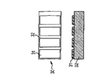
図3〜9に、多数のプロセスステップにおける各ステップ後の有機構成要素の外観を示す。各図では、多数のプロセスステップにおける有機構成要素30を示す。本プロセスでは、二つの犠牲層、層33,34が使用されている。
Figures 3-9 show the appearance of the organic components after each step in a number of process steps. Each figure shows the
図3に、有機構成要素30の平面図及び断面図を示す。図3に、フォイル等から形成され、任意で更にバリア層(例、Al2O3,SiO2,SiN3等の無機セラミックス、又はAl2O3/パリレン/Al2O3等の無機/有機のハイブリッド層)を有する基板32と、半透明の底部電極31とが示されている。バリア層は、基板と電極との間に存在する。バリア層は構成されていない。
In FIG. 3, the top view and sectional drawing of the
図4に、第一犠牲層33を製造及び構成した後に、更なるプロセスステップを実行した後の図3に示した有機構成要素を示す。第一犠牲層33は油又はフォトレジスト等であってもよく、次なるプロセスステップにて除去される。犠牲層の製造及び構成は、湿式リソグラフィー又は印刷等により実行され得る。
FIG. 4 shows the organic component shown in FIG. 3 after the first
図5に、更なるプロセスステップである第二犠牲層34の完成及び構成を示す。第二犠牲層34は、構成要素35の犠牲層33と他方の層とを損傷させないプロセスによって除去され得るように選択される。最後に図6に、ポリチオフェン/フラーレン等の半導体層からなる少なくとも一つの活性層35を有する大面積上に有機構成要素30が被覆される、更なるプロセスステップを示す。
FIG. 5 shows the completion and construction of the second
図7に、第二犠牲層34を除去した後の有機構成要素30を示す。犠牲層34は、蒸発等により除去され得る。基板32と底部電極31との上部に犠牲層33が今尚存在し、活性層35が基板32と全底部電極31及び第一犠牲層33を覆っている。
FIG. 7 shows the
図8に示すように、次いで構成要素30の大面積を、少なくとも一種の金属等からなる導電層36にて覆う。金属層36はアルミニウム、又はカルシウム/アルミニウム等の二層から構成され得る。
As shown in FIG. 8, the large area of the
最後に図9に、犠牲層33を除去した後の構成要素30の外観を示す。第一犠牲層はUV露出により、又は溶媒槽内で除去され得る。構成要素30は、Z接続して構成される。1個の基板32、底部電極31、半導体層35及び頂部電極36が図示されている。材料
に感光性が必要である場合、構成要素30を保護層で被覆してもよい。
Finally, FIG. 9 shows the appearance of the
図10〜13に、一つの犠牲層、即ち予備層を有する別の製造プロセスの例を示す。
図10に再び、半透明の底部電極31を有する基板32を示す。図11に、鋭利な、及び/又はネガティブなエッジを有するフォトレジスト等の構成予備層37が、湿式リソグラフィー又は印刷等のステップで塗布される方法を示す。
FIGS. 10 to 13 show an example of another manufacturing process having one sacrificial layer, that is, a preliminary layer.
FIG. 10 again shows a
図12に、ポリチオフェン/フラーレン混合物から形成された層38を、構成的印刷、又は大面積被覆し、その後の機械的プロセス、レーザ構成、(又は)リソグラフィープロセスによって5mm程度の間隔を隔てて、少なくとも一つの活性層上に塗布する方法を示す。少なくとも一つの活性層は、装置の一つ以上のモジュールを用いて塗布/堆積され得る。この活性層は有機半導体、有機導電体、ナノ粒子、無機半導体懸濁液、小粒子等からなり得る。
In FIG. 12, a
最後に図13にて、少なくとも一つの導電性金属層39が大面積塗布されているにも係らず、予備層37の鋭利な、又はネガティブなエッジにより薄膜が破裂するため、底部電極31部分が今尚露出されて、底部層内に自由空間が残留している状態を示す。図13に示すプロセスステップの後、最終的な構成要素30は、保護層により更に被覆かつ封止され得る。
Finally, in FIG. 13, the thin film is ruptured by the sharp or negative edge of the
本発明は、全体が巻回プロセスにより製造され得る有機構成要素の製造方法を、最初に開示するものである。本願に開示された連続的製造方法の更なる利点は、製造プロセスの任意の時点において、活性半導体層の活性領域が未保護溶媒、及び/又は溶媒蒸気に露出されないことである。それによって、高品質の有機構成要素が製造され得る。 The present invention first discloses a method of manufacturing an organic component that can be manufactured entirely by a winding process. A further advantage of the continuous manufacturing method disclosed herein is that the active region of the active semiconductor layer is not exposed to unprotected solvent and / or solvent vapor at any point in the manufacturing process. Thereby, high quality organic components can be produced.
Claims (5)
第一巻回体から基板を巻き出す第一の工程と、
巻き出された前記基板上に複数の第一の個別電極を形成する第二の工程と、
前記複数の第一の個別電極上に第一犠牲層を形成する第三の工程と、
第二犠牲層を前記基板上に形成する第四の工程と、
前記第一の個別電極上に有機半導体材料からなる有機半導体層を形成する第五の工程と、
前記第二犠牲層を除去することにより、前記有機半導体層を複数の有機半導体材料の個別部分に分割する第六の工程と、
前記複数の有機半導体材料の個別部分上に導電材料層を形成する第七の工程と、
前記第一犠牲層を除去することにより、前記導電材料層を複数の個別対向電極に分割する第八の工程と、
を備え、それによって、前記基板上に、前記第一の個別電極と前記有機半導体材料の個別部分と前記個別対向電極とを有する複数の光起電構成要素を形成し、
前記基板上に形成された複数の光起電構成要素を同基板とともに第二巻回体に巻き取るようにした、方法。 A method of manufacturing a photovoltaic component, the method comprising:
A first step of unwinding the substrate from the first wound body;
A second step of forming a plurality of first individual electrodes on the unwound substrate;
A third step of forming a first sacrificial layer on the plurality of first individual electrodes;
A fourth step of forming a second sacrificial layer on the substrate;
A fifth step of forming an organic semiconductor layer made of an organic semiconductor material on the first individual electrode;
A sixth step of dividing the organic semiconductor layer into individual portions of a plurality of organic semiconductor materials by removing the second sacrificial layer;
A seventh step of forming a conductive material layer on individual portions of the plurality of organic semiconductor materials;
An eighth step of dividing the conductive material layer into a plurality of individual counter electrodes by removing the first sacrificial layer;
Thereby forming, on the substrate, a plurality of photovoltaic components having the first individual electrode, the individual portion of the organic semiconductor material, and the individual counter electrode,
A method of winding a plurality of photovoltaic components formed on the substrate together with the substrate on a second winding body.
Applications Claiming Priority (2)
| Application Number | Priority Date | Filing Date | Title |
|---|---|---|---|
| DE102004024461.8 | 2004-05-14 | ||
| DE102004024461A DE102004024461A1 (en) | 2004-05-14 | 2004-05-14 | Device and method for producing an electronic component with at least one active organic layer |
Related Child Applications (1)
| Application Number | Title | Priority Date | Filing Date |
|---|---|---|---|
| JP2010274001A Division JP2011061238A (en) | 2004-05-14 | 2010-12-08 | Device and method for manufacturing electronic component with at least one active organic layer |
Publications (2)
| Publication Number | Publication Date |
|---|---|
| JP2006013456A JP2006013456A (en) | 2006-01-12 |
| JP5066326B2 true JP5066326B2 (en) | 2012-11-07 |
Family
ID=34936267
Family Applications (3)
| Application Number | Title | Priority Date | Filing Date |
|---|---|---|---|
| JP2005142201A Active JP5066326B2 (en) | 2004-05-14 | 2005-05-16 | Apparatus and method for producing an electronic component having at least one active organic layer |
| JP2010274001A Pending JP2011061238A (en) | 2004-05-14 | 2010-12-08 | Device and method for manufacturing electronic component with at least one active organic layer |
| JP2012259954A Active JP5547265B2 (en) | 2004-05-14 | 2012-11-28 | Method for producing an electronic component having at least one active organic layer |
Family Applications After (2)
| Application Number | Title | Priority Date | Filing Date |
|---|---|---|---|
| JP2010274001A Pending JP2011061238A (en) | 2004-05-14 | 2010-12-08 | Device and method for manufacturing electronic component with at least one active organic layer |
| JP2012259954A Active JP5547265B2 (en) | 2004-05-14 | 2012-11-28 | Method for producing an electronic component having at least one active organic layer |
Country Status (4)
| Country | Link |
|---|---|
| US (2) | US7476278B2 (en) |
| EP (1) | EP1596446A3 (en) |
| JP (3) | JP5066326B2 (en) |
| DE (1) | DE102004024461A1 (en) |
Families Citing this family (60)
| Publication number | Priority date | Publication date | Assignee | Title |
|---|---|---|---|---|
| US8329501B1 (en) | 2004-02-19 | 2012-12-11 | Nanosolar, Inc. | High-throughput printing of semiconductor precursor layer from inter-metallic microflake particles |
| US8372734B2 (en) | 2004-02-19 | 2013-02-12 | Nanosolar, Inc | High-throughput printing of semiconductor precursor layer from chalcogenide nanoflake particles |
| US8846141B1 (en) | 2004-02-19 | 2014-09-30 | Aeris Capital Sustainable Ip Ltd. | High-throughput printing of semiconductor precursor layer from microflake particles |
| US7604843B1 (en) | 2005-03-16 | 2009-10-20 | Nanosolar, Inc. | Metallic dispersion |
| US7700464B2 (en) | 2004-02-19 | 2010-04-20 | Nanosolar, Inc. | High-throughput printing of semiconductor precursor layer from nanoflake particles |
| US8309163B2 (en) | 2004-02-19 | 2012-11-13 | Nanosolar, Inc. | High-throughput printing of semiconductor precursor layer by use of chalcogen-containing vapor and inter-metallic material |
| US7663057B2 (en) | 2004-02-19 | 2010-02-16 | Nanosolar, Inc. | Solution-based fabrication of photovoltaic cell |
| US7605328B2 (en) | 2004-02-19 | 2009-10-20 | Nanosolar, Inc. | Photovoltaic thin-film cell produced from metallic blend using high-temperature printing |
| US8623448B2 (en) | 2004-02-19 | 2014-01-07 | Nanosolar, Inc. | High-throughput printing of semiconductor precursor layer from chalcogenide microflake particles |
| DE102006026981A1 (en) * | 2006-06-10 | 2007-12-13 | Leonhard Kurz Gmbh & Co. Kg | Method for producing a structured layer on a carrier substrate |
| DE102006027292B4 (en) * | 2006-06-13 | 2010-06-17 | Leonhard Kurz Gmbh & Co. Kg | Process for producing a structured layer sequence on a substrate |
| DE102006027291B4 (en) * | 2006-06-13 | 2010-06-17 | Leonhard Kurz Gmbh & Co. Kg | Process for producing a structured layer sequence on a substrate |
| US9112447B2 (en) * | 2006-11-03 | 2015-08-18 | Solera Laboratories, Inc. | Nano power cell and method of use |
| US8319092B1 (en) | 2006-11-03 | 2012-11-27 | Solera Laboratories, Inc. | Nano power cell and method of use |
| US8053260B2 (en) * | 2006-11-17 | 2011-11-08 | General Electric Company | Large-area lighting systems and methods of making the same |
| US7704352B2 (en) * | 2006-12-01 | 2010-04-27 | Applied Materials, Inc. | High-aspect ratio anode and apparatus for high-speed electroplating on a solar cell substrate |
| US20080128019A1 (en) * | 2006-12-01 | 2008-06-05 | Applied Materials, Inc. | Method of metallizing a solar cell substrate |
| US7799182B2 (en) | 2006-12-01 | 2010-09-21 | Applied Materials, Inc. | Electroplating on roll-to-roll flexible solar cell substrates |
| US7736928B2 (en) * | 2006-12-01 | 2010-06-15 | Applied Materials, Inc. | Precision printing electroplating through plating mask on a solar cell substrate |
| US8153889B2 (en) * | 2007-01-22 | 2012-04-10 | Solopower, Inc. | Roll-to-roll integration of thin film solar modules |
| DE102007060108B4 (en) | 2007-12-13 | 2011-07-21 | LEONHARD KURZ Stiftung & Co. KG, 90763 | Method for producing a solar cell module |
| JP5172402B2 (en) * | 2008-03-13 | 2013-03-27 | シャープ株式会社 | Organic EL device |
| US20100126849A1 (en) * | 2008-11-24 | 2010-05-27 | Applied Materials, Inc. | Apparatus and method for forming 3d nanostructure electrode for electrochemical battery and capacitor |
| DE102009053733A1 (en) | 2009-11-18 | 2011-05-19 | Daimler Ag | Motor vehicle component comprises shielding element formed as micro-structured surface structure and constructed from a pixel of conductive, magnetic and magnetizable materials for shielding electrical, magnetic and electromagnetic fields |
| DE102009053767A1 (en) | 2009-11-18 | 2011-05-19 | Daimler Ag | Motor vehicle component, has photovoltaic element formed as microstructure element on surface of component, where reflector element is arranged between photovoltaic element and component surface |
| DE102009053768A1 (en) | 2009-11-18 | 2011-05-19 | Daimler Ag | Motor vehicle component, has photovoltaic element formed on surface of component, and optically active structural element i.e. convex micro optical element, provided within and/or adjacent to photovoltaic element |
| DE102009053771A1 (en) | 2009-11-18 | 2011-05-19 | Daimler Ag | Vehicle component, has photovoltaic element designed as microstructured surface structure of component, where microstructured surface is formed from individual pixels made of two different materials for obtaining photovoltaic effect |
| DE102009053765A1 (en) | 2009-11-18 | 2011-05-19 | Daimler Ag | Motor vehicle component, has photovoltaic element connected with power supply, of motor vehicle by conductive path and/or contacting element, which are formed as micro-structured surface structure comprising pixels |
| JP2011124231A (en) * | 2009-12-03 | 2011-06-23 | Novaled Ag | Method of forming electrical interconnect in organic optical electronic device, method of manufacturing organic optical electronic device, and organic light-emitting device |
| EP2355199B1 (en) * | 2010-01-29 | 2017-07-05 | Novaled GmbH | A method for producing an organic light emitting device |
| US20120281980A1 (en) * | 2010-01-29 | 2012-11-08 | Cho Hans S | Optical sensor networks and methods for fabricating the same |
| TWI424576B (en) * | 2010-04-30 | 2014-01-21 | Axuntek Solar Energy | See-through solar battery module and manufacturing method thereof |
| CN102237374B (en) * | 2010-05-04 | 2013-06-05 | 绿阳光电股份有限公司 | Transmission solar cell module and method for manufacturing same |
| WO2012073650A1 (en) * | 2010-11-30 | 2012-06-07 | 株式会社カネカ | Organic el device |
| EP2647050B1 (en) * | 2010-12-03 | 2018-04-11 | Novaled GmbH | Method for forming an electrical interconnection in an organic photovoltaic device and an organic photovoltaic device made by the same |
| WO2012093467A1 (en) * | 2011-01-06 | 2012-07-12 | シャープ株式会社 | Organic el display device and method for manufacturing same |
| KR101608565B1 (en) * | 2011-02-24 | 2016-04-01 | 가부시키가이샤 니콘 | Device for transporting flexible substrate, and system for manufacturing display device or electrical circuit |
| EP2506330A1 (en) | 2011-04-01 | 2012-10-03 | Nederlandse Organisatie voor toegepast -natuurwetenschappelijk onderzoek TNO | Apparatus and method for providing an embedded structure and for providing an electro-optical device including the same |
| EP2702048B1 (en) | 2011-04-28 | 2019-01-23 | Merck Patent GmbH | Novel photoactive polymers |
| JP2014513443A (en) | 2011-05-09 | 2014-05-29 | メルク パテント ゲーエムベーハー | Multi-junction photovoltaic cell |
| EP2528097A1 (en) | 2011-05-27 | 2012-11-28 | Nederlandse Organisatie voor toegepast -natuurwetenschappelijk onderzoek TNO | Photovoltaic device and method of manufacturing the same |
| US8674377B2 (en) * | 2011-08-30 | 2014-03-18 | General Electric Company | Optoelectronic device package, array and method of fabrication |
| JP5745973B2 (en) * | 2011-09-02 | 2015-07-08 | 日立造船株式会社 | Thin-film solar cell manufacturing apparatus and manufacturing method |
| KR101305660B1 (en) * | 2011-10-17 | 2013-09-09 | 엘지이노텍 주식회사 | Solar cell module and method of fabricating the same |
| WO2013137274A1 (en) * | 2012-03-12 | 2013-09-19 | 三菱化学株式会社 | Method for manufacturing organic thin-film solar-cell module, and organic thin-film solar-cell module |
| US20130263925A1 (en) | 2012-04-05 | 2013-10-10 | Merck Patent Gmbh | Hole Carrier Layer For Organic Photovoltaic Device |
| WO2013152952A1 (en) * | 2012-04-10 | 2013-10-17 | Danmarks Tekniske Universitet | A photovoltaic module |
| DE102012106607B4 (en) | 2012-07-20 | 2024-04-04 | Heliatek Gmbh | Method for sealing modules with optoelectronic components |
| JP6179201B2 (en) * | 2013-06-05 | 2017-08-16 | 三菱ケミカル株式会社 | Manufacturing method of organic thin film solar cell |
| CN103611653B (en) * | 2013-12-13 | 2015-09-16 | 厦门惟华光能有限公司 | Organic solar batteries test coating machine |
| DE102013226280A1 (en) | 2013-12-17 | 2015-06-18 | Belectric Opv Gmbh | Organic photovoltaic element, and method for producing such |
| EP2947697A1 (en) | 2013-12-23 | 2015-11-25 | Merck Patent GmbH | Antireflection films and photovoltaic devices |
| DE102014004323B4 (en) | 2014-03-25 | 2021-11-11 | Gottfried Wilhelm Leibniz Universität Hannover | Coating device for at least partially coating a surface |
| KR20160000192A (en) * | 2014-06-24 | 2016-01-04 | 코오롱인더스트리 주식회사 | Photovoltaics module package and the manufacturing method thereof |
| DE102014213978A1 (en) | 2014-07-17 | 2016-01-21 | Belectric Opv Gmbh | Process for producing an organic semiconductor device and organic semiconductor device |
| EP3198660B1 (en) | 2014-09-26 | 2022-07-06 | Heliatek GmbH | Method for applying a protective layer for the fabrication of a semi-finished product |
| EP3523835B1 (en) | 2016-10-05 | 2022-11-16 | Raynergy Tek Inc. | Organic photodetector |
| DE102017215197B3 (en) | 2017-08-30 | 2018-12-27 | Opvius Gmbh | Semiconductor module and method for producing a semiconductor module |
| US11456397B2 (en) | 2019-03-12 | 2022-09-27 | E Ink Corporation | Energy harvesting electro-optic displays |
| DE102020123252A1 (en) | 2019-12-12 | 2021-06-17 | Heliatek Gmbh | Coating for an optoelectronic component, method for producing such a coating, optoelectronic component with such a coating |
Family Cites Families (43)
| Publication number | Priority date | Publication date | Assignee | Title |
|---|---|---|---|---|
| US4606931A (en) * | 1983-06-27 | 1986-08-19 | International Business Machines Corporation | Lift-off masking method |
| JPS60173842A (en) * | 1984-02-20 | 1985-09-07 | Canon Inc | Forming method of pattern |
| JPS61139075A (en) * | 1984-12-11 | 1986-06-26 | Ricoh Co Ltd | Manufacture of photoelectric conversion element |
| EP0193820A3 (en) * | 1985-02-27 | 1988-01-07 | Kanegafuchi Kagaku Kogyo Kabushiki Kaisha | Method for forming a thin film pattern |
| JPH02148715A (en) * | 1988-11-29 | 1990-06-07 | Canon Inc | Apparatus for forming semiconductor device continuously |
| JP2810532B2 (en) * | 1990-11-29 | 1998-10-15 | キヤノン株式会社 | Method and apparatus for forming deposited film |
| EP0609104B1 (en) * | 1993-01-29 | 1998-05-20 | Canon Kabushiki Kaisha | Process for the formation of functional deposited films |
| JP3571785B2 (en) * | 1993-12-28 | 2004-09-29 | キヤノン株式会社 | Method and apparatus for forming deposited film |
| JP3272188B2 (en) * | 1995-05-17 | 2002-04-08 | 三洋電機株式会社 | Method for manufacturing thin film semiconductor device |
| EP1045454A4 (en) * | 1998-07-27 | 2001-10-24 | Citizen Watch Co Ltd | Solar cell and method of producing the same, and mask for photolithography for producing solar cell |
| US6228228B1 (en) * | 1999-02-23 | 2001-05-08 | Sarnoff Corporation | Method of making a light-emitting fiber |
| EP1115268A1 (en) * | 1999-07-07 | 2001-07-11 | Sony Corporation | Method and apparatus for manufacturing flexible organic el display |
| US6315820B1 (en) * | 1999-10-19 | 2001-11-13 | Ford Global Technologies, Inc. | Method of manufacturing thin metal alloy foils |
| US6372538B1 (en) * | 2000-03-16 | 2002-04-16 | University Of Delaware | Fabrication of thin-film, flexible photovoltaic module |
| JP4316767B2 (en) * | 2000-03-22 | 2009-08-19 | 株式会社半導体エネルギー研究所 | Substrate processing equipment |
| DE10017610C2 (en) * | 2000-03-30 | 2002-10-31 | Hahn Meitner Inst Berlin Gmbh | Process for producing a solar module with integrated series-connected thin-film solar cells and use thereof |
| US7022910B2 (en) * | 2002-03-29 | 2006-04-04 | Konarka Technologies, Inc. | Photovoltaic cells utilizing mesh electrodes |
| SE0103740D0 (en) * | 2001-11-08 | 2001-11-08 | Forskarpatent I Vaest Ab | Photovoltaic element and production methods |
| US6867539B1 (en) * | 2000-07-12 | 2005-03-15 | 3M Innovative Properties Company | Encapsulated organic electronic devices and method for making same |
| JP2002170669A (en) * | 2000-12-01 | 2002-06-14 | Tdk Corp | Organic el display device and its manufacturing method |
| US6819316B2 (en) * | 2001-04-17 | 2004-11-16 | 3M Innovative Properties Company | Flexible capacitive touch sensor |
| US7323635B2 (en) * | 2001-06-15 | 2008-01-29 | University Of Massachusetts | Photovoltaic cell |
| US20020195928A1 (en) * | 2001-06-25 | 2002-12-26 | Grace Anthony J. | Electroluminescent display device and method of making |
| JP4219807B2 (en) * | 2001-08-09 | 2009-02-04 | 旭化成株式会社 | Organic semiconductor device |
| JP4336869B2 (en) * | 2001-11-27 | 2009-09-30 | 日本電気株式会社 | Vacuum film forming apparatus, vacuum film forming method, and battery electrode manufacturing method |
| US6555284B1 (en) * | 2001-12-27 | 2003-04-29 | Eastman Kodak Company | In situ vacuum method for making OLED devices |
| WO2003065472A2 (en) * | 2002-01-25 | 2003-08-07 | Konarka Technologies, Inc. | Structures and materials for dye sensitized solar cells |
| EP1351321B1 (en) * | 2002-04-01 | 2013-12-25 | Konica Corporation | Support and organic electroluminescence element comprising the support |
| US8808457B2 (en) * | 2002-04-15 | 2014-08-19 | Samsung Display Co., Ltd. | Apparatus for depositing a multilayer coating on discrete sheets |
| US7396493B2 (en) * | 2002-05-21 | 2008-07-08 | 3M Innovative Properties Company | Multilayer optical film with melt zone to control delamination |
| US6943066B2 (en) * | 2002-06-05 | 2005-09-13 | Advantech Global, Ltd | Active matrix backplane for controlling controlled elements and method of manufacture thereof |
| US6946597B2 (en) * | 2002-06-22 | 2005-09-20 | Nanosular, Inc. | Photovoltaic devices fabricated by growth from porous template |
| AU2003252952A1 (en) * | 2002-08-06 | 2004-02-23 | Avecia Limited | Organic electronic devices |
| US7247346B1 (en) * | 2002-08-28 | 2007-07-24 | Nanosolar, Inc. | Combinatorial fabrication and high-throughput screening of optoelectronic devices |
| GB2395358B (en) * | 2002-09-17 | 2006-08-02 | Dainippon Printing Co Ltd | Method of manufacturing a light emitting display panel and a light emitting display panel |
| US7080901B2 (en) * | 2002-12-03 | 2006-07-25 | Dai Nippon Printing Co. Ltd. | Printing unit and manufacturing line for manufacturing flexible organic EL display |
| US20040118444A1 (en) * | 2002-12-20 | 2004-06-24 | General Electric Company | Large-area photovoltaic devices and methods of making same |
| GB0229653D0 (en) * | 2002-12-20 | 2003-01-22 | Cambridge Display Tech Ltd | Electrical connection of optoelectronic devices |
| US6833201B2 (en) * | 2003-01-31 | 2004-12-21 | Clemson University | Nanostructured-doped compound for use in an EL element |
| US7153180B2 (en) * | 2003-11-13 | 2006-12-26 | Eastman Kodak Company | Continuous manufacture of flat panel light emitting devices |
| US20050164425A1 (en) * | 2004-01-23 | 2005-07-28 | Markus Tuomikoski | Optoelectronic component |
| US7122398B1 (en) * | 2004-03-25 | 2006-10-17 | Nanosolar, Inc. | Manufacturing of optoelectronic devices |
| US6967115B1 (en) * | 2004-04-20 | 2005-11-22 | Nanosolor, Inc. | Device transfer techniques for thin film optoelectronic devices |
-
2004
- 2004-05-14 DE DE102004024461A patent/DE102004024461A1/en not_active Ceased
-
2005
- 2005-05-09 EP EP05010008A patent/EP1596446A3/en not_active Ceased
- 2005-05-11 US US11/127,439 patent/US7476278B2/en active Active - Reinstated
- 2005-05-16 JP JP2005142201A patent/JP5066326B2/en active Active
-
2007
- 2007-07-20 US US11/780,951 patent/US8129616B2/en active Active
-
2010
- 2010-12-08 JP JP2010274001A patent/JP2011061238A/en active Pending
-
2012
- 2012-11-28 JP JP2012259954A patent/JP5547265B2/en active Active
Also Published As
| Publication number | Publication date |
|---|---|
| JP2013084968A (en) | 2013-05-09 |
| DE102004024461A1 (en) | 2005-12-01 |
| JP5547265B2 (en) | 2014-07-09 |
| US20070295400A1 (en) | 2007-12-27 |
| JP2006013456A (en) | 2006-01-12 |
| US20050272263A1 (en) | 2005-12-08 |
| JP2011061238A (en) | 2011-03-24 |
| EP1596446A3 (en) | 2008-07-09 |
| EP1596446A2 (en) | 2005-11-16 |
| US8129616B2 (en) | 2012-03-06 |
| US7476278B2 (en) | 2009-01-13 |
Similar Documents
| Publication | Publication Date | Title |
|---|---|---|
| JP5066326B2 (en) | Apparatus and method for producing an electronic component having at least one active organic layer | |
| DE10318187B4 (en) | Encapsulation method for organic light emitting diode devices | |
| DE10362210B4 (en) | Method for encapsulating an organic light emitting diode device | |
| DE60010531T2 (en) | STRUCTURING OF ELECTRODES IN OLED COMPONENTS | |
| JP5834009B2 (en) | Monolithic parallel interconnect structure | |
| CN111969034A (en) | Display panel and preparation method thereof | |
| DE69937407T2 (en) | CAPTURE OF A DEVICE | |
| EP2609641B1 (en) | Self-aligned coverage of opaque conductive areas | |
| US20090056801A1 (en) | Thin film solar cell and manufacturing method thereof | |
| US9824821B2 (en) | Thin film capacitor with intermediate electrodes | |
| KR100986024B1 (en) | Method for manufacturing transparent electrode pattern and method for manufacturing optical device | |
| CN106663703A (en) | Flexible substrate material and method of fabricating an electronic thin film device | |
| KR20120125280A (en) | Method of maskless manufacturing of oled devices | |
| KR101894327B1 (en) | Organic Emitting Display Device and Method for Manufacturing the Same | |
| KR20190140405A (en) | Method for manufacturing a photovoltaic module and photovoltaic module thus obtained | |
| DE102016109485A1 (en) | METHOD FOR PRODUCING AN OPTOELECTRONIC COMPONENT, OPTOELECTRONIC COMPONENT AND PROTECTIVE LAYER | |
| DE102012109218A1 (en) | Method for producing an optoelectronic assembly and optoelectronic assembly | |
| US10121990B2 (en) | Organic light emitting devices and methods of fabricating the same | |
| JP2011034931A (en) | Organic el display device | |
| CN112537754B (en) | Electrical isolation structure and preparation method thereof | |
| JP6072692B2 (en) | Method for manufacturing an organic electronic device | |
| DE102013205714A1 (en) | ORGANIC COMPONENT AND MANUFACTURING METHOD | |
| WO2016146438A1 (en) | Method for producing an optoelectronic component | |
| DE102012109142B4 (en) | Method for producing a passive electronic component and method for producing an optoelectronic assembly | |
| CN114420861A (en) | Display panel and manufacturing method thereof |
Legal Events
| Date | Code | Title | Description |
|---|---|---|---|
| A621 | Written request for application examination |
Free format text: JAPANESE INTERMEDIATE CODE: A621 Effective date: 20080317 |
|
| A977 | Report on retrieval |
Free format text: JAPANESE INTERMEDIATE CODE: A971007 Effective date: 20100531 |
|
| A131 | Notification of reasons for refusal |
Free format text: JAPANESE INTERMEDIATE CODE: A131 Effective date: 20100608 |
|
| A601 | Written request for extension of time |
Free format text: JAPANESE INTERMEDIATE CODE: A601 Effective date: 20100908 |
|
| A602 | Written permission of extension of time |
Free format text: JAPANESE INTERMEDIATE CODE: A602 Effective date: 20100913 |
|
| A601 | Written request for extension of time |
Free format text: JAPANESE INTERMEDIATE CODE: A601 Effective date: 20101008 |
|
| A602 | Written permission of extension of time |
Free format text: JAPANESE INTERMEDIATE CODE: A602 Effective date: 20101014 |
|
| A601 | Written request for extension of time |
Free format text: JAPANESE INTERMEDIATE CODE: A601 Effective date: 20101108 |
|
| A602 | Written permission of extension of time |
Free format text: JAPANESE INTERMEDIATE CODE: A602 Effective date: 20101111 |
|
| A521 | Request for written amendment filed |
Free format text: JAPANESE INTERMEDIATE CODE: A523 Effective date: 20101208 |
|
| A02 | Decision of refusal |
Free format text: JAPANESE INTERMEDIATE CODE: A02 Effective date: 20110802 |
|
| A521 | Request for written amendment filed |
Free format text: JAPANESE INTERMEDIATE CODE: A523 Effective date: 20111130 |
|
| A521 | Request for written amendment filed |
Free format text: JAPANESE INTERMEDIATE CODE: A523 Effective date: 20111207 |
|
| A911 | Transfer to examiner for re-examination before appeal (zenchi) |
Free format text: JAPANESE INTERMEDIATE CODE: A911 Effective date: 20120110 |
|
| RD04 | Notification of resignation of power of attorney |
Free format text: JAPANESE INTERMEDIATE CODE: A7424 Effective date: 20120126 |
|
| A131 | Notification of reasons for refusal |
Free format text: JAPANESE INTERMEDIATE CODE: A131 Effective date: 20120207 |
|
| A521 | Request for written amendment filed |
Free format text: JAPANESE INTERMEDIATE CODE: A523 Effective date: 20120502 |
|
| TRDD | Decision of grant or rejection written | ||
| A01 | Written decision to grant a patent or to grant a registration (utility model) |
Free format text: JAPANESE INTERMEDIATE CODE: A01 Effective date: 20120529 |
|
| A01 | Written decision to grant a patent or to grant a registration (utility model) |
Free format text: JAPANESE INTERMEDIATE CODE: A01 |
|
| R155 | Notification before disposition of declining of application |
Free format text: JAPANESE INTERMEDIATE CODE: R155 |
|
| A61 | First payment of annual fees (during grant procedure) |
Free format text: JAPANESE INTERMEDIATE CODE: A61 Effective date: 20120813 |
|
| R150 | Certificate of patent or registration of utility model |
Free format text: JAPANESE INTERMEDIATE CODE: R150 Ref document number: 5066326 Country of ref document: JP Free format text: JAPANESE INTERMEDIATE CODE: R150 |
|
| FPAY | Renewal fee payment (event date is renewal date of database) |
Free format text: PAYMENT UNTIL: 20150817 Year of fee payment: 3 |
|
| FPAY | Renewal fee payment (event date is renewal date of database) |
Free format text: PAYMENT UNTIL: 20150817 Year of fee payment: 3 |
|
| S111 | Request for change of ownership or part of ownership |
Free format text: JAPANESE INTERMEDIATE CODE: R313113 |
|
| FPAY | Renewal fee payment (event date is renewal date of database) |
Free format text: PAYMENT UNTIL: 20150817 Year of fee payment: 3 |
|
| R350 | Written notification of registration of transfer |
Free format text: JAPANESE INTERMEDIATE CODE: R350 |
|
| R250 | Receipt of annual fees |
Free format text: JAPANESE INTERMEDIATE CODE: R250 |
|
| R250 | Receipt of annual fees |
Free format text: JAPANESE INTERMEDIATE CODE: R250 |
|
| R250 | Receipt of annual fees |
Free format text: JAPANESE INTERMEDIATE CODE: R250 |
|
| R250 | Receipt of annual fees |
Free format text: JAPANESE INTERMEDIATE CODE: R250 |
|
| R250 | Receipt of annual fees |
Free format text: JAPANESE INTERMEDIATE CODE: R250 |
|
| R250 | Receipt of annual fees |
Free format text: JAPANESE INTERMEDIATE CODE: R250 |
|
| R250 | Receipt of annual fees |
Free format text: JAPANESE INTERMEDIATE CODE: R250 |
|
| R250 | Receipt of annual fees |
Free format text: JAPANESE INTERMEDIATE CODE: R250 |
|
| S111 | Request for change of ownership or part of ownership |
Free format text: JAPANESE INTERMEDIATE CODE: R313113 |
|
| R350 | Written notification of registration of transfer |
Free format text: JAPANESE INTERMEDIATE CODE: R350 |
|
| R250 | Receipt of annual fees |
Free format text: JAPANESE INTERMEDIATE CODE: R250 |