JP5065772B2 - Plasma processing apparatus member and manufacturing method thereof - Google Patents
Plasma processing apparatus member and manufacturing method thereof Download PDFInfo
- Publication number
- JP5065772B2 JP5065772B2 JP2007153269A JP2007153269A JP5065772B2 JP 5065772 B2 JP5065772 B2 JP 5065772B2 JP 2007153269 A JP2007153269 A JP 2007153269A JP 2007153269 A JP2007153269 A JP 2007153269A JP 5065772 B2 JP5065772 B2 JP 5065772B2
- Authority
- JP
- Japan
- Prior art keywords
- plasma processing
- processing apparatus
- film
- anodized film
- lower electrode
- Prior art date
- Legal status (The legal status is an assumption and is not a legal conclusion. Google has not performed a legal analysis and makes no representation as to the accuracy of the status listed.)
- Expired - Fee Related
Links
Images

Description
本発明は、半導体装置および液晶表示装置を製造するための、成膜やエッチング等を行うプラズマ処理装置を構成するプラズマ処理装置用部材に関する。 The present invention relates to a member for a plasma processing apparatus that constitutes a plasma processing apparatus that performs film formation, etching, and the like for manufacturing a semiconductor device and a liquid crystal display device.
半導体装置、液晶表示装置を製造するための、成膜やエッチング等を行うプラズマ処理装置を構成する部材には、多くのアルミニウム部材が使用されている。成膜処理装置であるCVD(Chemical Vapor Deposition:気相化学成長)装置の、処理室内の上部と下部にそれぞれ設置される上部電極と下部電極は、その一部である。これらの電極となる部材は、ソースガス等に対する高い耐食性が要求されると共に、電極の表面形状がプロセスの均一性および安定性に大きく影響するため、その制御には様々な工夫がなされている。 Many aluminum members are used as members constituting a plasma processing apparatus that performs film formation, etching, and the like for manufacturing semiconductor devices and liquid crystal display devices. An upper electrode and a lower electrode, which are respectively installed at an upper part and a lower part in a processing chamber of a CVD (Chemical Vapor Deposition) apparatus which is a film forming apparatus, are a part thereof. These electrodes are required to have high corrosion resistance against the source gas and the like, and the surface shape of the electrode greatly affects the uniformity and stability of the process.
特に、CVD装置の下部電極は、ウエハやガラス基板等のワークが直接載置された状態で成膜処理が行われるため、その表面形状による成膜への影響は大きい。成膜処理において、ワークが静電吸着により下部電極に貼り付いて離れない「スティッキング」が発生することがある。このスティッキングにより、成膜処理後に下部電極からワークを移送する際、CVD装置のワーク支持部材やワークが破損する虞があるため、スティッキングを防止する(耐スティッキング性を備える)ため下部電極の表面にブラスト(粗化)処理を施す等の、ワークとの接触面積を減らすための処理が施されている。 Particularly, the lower electrode of the CVD apparatus has a great influence on the film formation due to its surface shape because the film formation process is performed in a state where a workpiece such as a wafer or a glass substrate is directly placed. In the film forming process, “sticking” may occur in which the workpiece is stuck to the lower electrode due to electrostatic adsorption and does not leave. When the workpiece is transferred from the lower electrode after the film formation process due to this sticking, the workpiece support member of the CVD apparatus or the workpiece may be damaged. Therefore, the sticking is prevented from occurring on the surface of the lower electrode. Processing for reducing the contact area with the workpiece, such as blasting (roughening), is performed.
しかしながら、このような下部電極は、その表面にブラスト処理によって急峻な突起が形成されている。そして、この突起はワークとの接触によって磨耗し、塵芥となって汚染の原因となる。さらに、磨耗によって下部電極の表面形状が変化することで、下部電極からワークへの熱伝導が変化、すなわち成膜条件が変化して、形成された膜に悪影響を及ぼす。そこで、特許文献1には、ブラスト処理後に表面を研磨処理して表面粗さを維持しつつ急峻な突起を除去する技術が開示されている。また、特許文献2には、表面に波打ち形状等のパターンの凹凸を形成してワークとの接触面積を減らす技術が開示されている。
しかしながら、特許文献1のようにブラスト処理を行った下部電極には不可避的に残留応力が生じ、下部電極が反ってワークを安定して支持できないことがある。また、特許文献2のように、パターン化した凹凸が形成された下部電極では、このパターンに沿ってワークに成膜ムラを生じる虞がある。すなわち、上記従来技術では、耐スティッキング性を備えつつ、下部電極として優れた性能を備えた部材は得られなかった。
However, there are cases where residual stress is inevitably generated in the lower electrode subjected to the blasting process as in
また、CVD装置の上部電極および下部電極に代表されるプラズマ処理装置用部材は、静電気を帯びた状態でプラズマ処理を行うと、部材における微小欠陥等の電気的に弱い部分に局所的に電気が集中し、異常放電等の不具合が生じる虞がある。 Further, when a plasma processing apparatus member represented by an upper electrode and a lower electrode of a CVD apparatus is subjected to plasma processing in a state of being charged with static electricity, a local electric current is applied to an electrically weak portion such as a micro defect in the member. Concentration may cause problems such as abnormal discharge.
本発明は、前記問題点に鑑みてなされたものであり、耐スティッキング性に優れ、CVD装置の下部電極等のワーク載置部材として好適かつ安定した形状を備え、プラズマ処理時の異常放電を抑制することが可能なプラズマ処理装置用部材を提供することを目的とする。 The present invention has been made in view of the above problems, has excellent anti-sticking properties, has a suitable and stable shape as a workpiece mounting member such as a lower electrode of a CVD apparatus, and suppresses abnormal discharge during plasma processing. An object of the present invention is to provide a member for a plasma processing apparatus that can be used.
前記課題を解決するために、請求項1に係るプラズマ処理装置用部材は、ワークにプラズマ処理を施すプラズマ処理装置の前記ワークを載置する電極として用いられるプラズマ処理装置用部材であって、アルミニウムまたはアルミニウム合金からなる基材と前記基材の表面に形成された陽極酸化皮膜とを備え、前記陽極酸化皮膜は、印加電圧100V時のリーク電流密度が0.9×10⁻⁵A/cm2を超え、膜厚が3μm以上、表面の算術平均粗さが1μm未満であって、前記陽極酸化皮膜を形成された表面の平面度が50μm以下であることを特徴とする。
The problem to solve, member for a plasma processing apparatus according to
このような構成によれば、基材の表面に所定の厚さの陽極酸化皮膜を備えることで、プラズマ処理装置用部材に耐食性を備えることができる。また、陽極酸化皮膜が上記所定を超えるリーク電流密度を有することにより、プラズマ処理時にプラズマ処理装置用部材に帯電する電荷が少なくなり、ワークの、下部電極であるプラズマ処理装置用部材への静電吸着が抑制される。同時に、プラズマ処理装置用部材の電荷分布が均一となって、電気的に集中する部分が少なくなる。また、陽極酸化皮膜の表面すなわちプラズマ処理装置用部材の表面を平滑にすることで、均一かつ安定した成膜が可能となる。 According to such a configuration, the plasma processing apparatus member can be provided with corrosion resistance by providing the surface of the base material with the anodic oxide film having a predetermined thickness. In addition, since the anodized film has a leakage current density exceeding the predetermined value, the charge charged to the plasma processing apparatus member during plasma processing is reduced, and the workpiece is electrostatically charged to the plasma processing apparatus member as the lower electrode. Adsorption is suppressed. At the same time, the electric charge distribution of the plasma processing apparatus member becomes uniform, and there are fewer electrically concentrated portions. Further, by smoothing the surface of the anodic oxide film, that is, the surface of the member for the plasma processing apparatus, uniform and stable film formation is possible.
さらに、請求項2に係るプラズマ処理装置用部材は、請求項1に記載のプラズマ処理装置用部材において、前記陽極酸化皮膜が、リン酸−クロム酸浸漬試験における溶解速度が、100mg/dm2/15min未満であることを特徴とする。
Furthermore, the member for a plasma processing apparatus according to claim 2 is the member for a plasma processing apparatus according to
このような陽極酸化皮膜のリン酸−クロム酸浸漬試験により、陽極酸化皮膜が水和されて少なくとも一部がベーマイトおよび/または擬ベーマイト化していると判定することが可能であり、この水和処理を制御することによって陽極酸化皮膜に微細なクラックを形成することができ、その結果、リーク電流密度を制御することができる。 By such a phosphoric acid-chromic acid immersion test of the anodized film, it is possible to determine that the anodized film is hydrated and at least a part thereof is boehmite and / or pseudoboehmite. By controlling the above, fine cracks can be formed in the anodized film, and as a result, the leakage current density can be controlled.
さらに、請求項3に係るプラズマ処理装置用部材は、請求項1または請求項2に記載のプラズマ処理装置用部材において、前記陽極酸化皮膜の表面の算術平均粗さが、プラズマ処理装置用部材の半径方向における表面の算術平均粗さであることを特徴とする。
Furthermore, the member for a plasma processing apparatus according to claim 3 is the member for a plasma processing apparatus according to
このように、プラズマ処理装置用部材の半径方向に沿って測定した表面粗さの算術平均粗さを制御することにより、均一な成膜処理を実現する下部電極とすることが可能となる。 Thus, by controlling the arithmetic average roughness of the surface roughness measured along the radial direction of the member for a plasma processing apparatus, it is possible to obtain a lower electrode that realizes a uniform film forming process.
また、請求項4に係るプラズマ処理装置用部材は、請求項1ないし請求項3のいずれか一項に記載のプラズマ処理装置用部材において、前記陽極酸化皮膜を形成された表面の形状が同心円状に高さの変化した凹面または凸面のいずれかであることを特徴とする。
The plasma processing apparatus member according to
このように、プラズマ処理装置用部材の中心から同心円状に表面の高さ位置が変化する凹面または凸面のいずれかにすることにより、ワークが安定して載置される下部電極とすることが可能となる。 In this way, it is possible to provide a lower electrode on which a workpiece is stably placed by using either a concave surface or a convex surface whose surface height position changes concentrically from the center of the plasma processing apparatus member. It becomes.
また、請求項5に係るプラズマ処理装置用部材の製造方法は、請求項1ないし請求項4のいずれか一項に記載のプラズマ処理装置用部材の製造方法であって、表面加工工程(機械的切削)、陽極酸化処理工程、加水処理工程(水和処理工程)をこの順に行うことを特徴とする。
Moreover, the manufacturing method of the member for plasma processing apparatuses which concerns on
このような製造方法により、表面が平滑で、微細クラックが形成された陽極酸化皮膜を備えたプラズマ処理装置用部材が得られる。 By such a manufacturing method, a member for a plasma processing apparatus provided with an anodized film having a smooth surface and formed with fine cracks can be obtained.
請求項1に係るプラズマ処理装置用部材によれば、耐食性および耐スティッキング性を備え、異常放電を抑制し、均一かつ安定した成膜が可能となる。また、請求項2に係るプラズマ処理装置用部材によれば、陽極酸化皮膜のリーク電流密度を制御することが容易となり、耐スティッキング性および異常放電抑制効果をさらに向上させることが可能となる。
The member for a plasma processing apparatus according to
請求項3、請求項4に係るプラズマ処理装置用部材によれば、CVD装置の下部電極として好適な表面形状に制御できる。
According to the member for a plasma processing apparatus according to
請求項5に係るプラズマ処理装置用部材の製造方法によれば、上記プラズマ処理装置用部材を容易に製造できる。
According to the method for manufacturing a member for a plasma processing apparatus according to
以下、本発明に係るプラズマ処理装置用部材の構成について説明する。
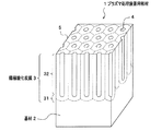
図1は、本発明の実施の形態であるプラズマ処理装置用部材の一部を拡大した模式図、図2は、本発明の実施の形態であるプラズマ処理装置用部材の表面形状を説明する断面模式図である。図1に示すように、プラズマ処理装置用部材1は、アルミニウムまたはアルミニウム合金からなる基材2と基材2の表面に形成された陽極酸化皮膜3とを備える。以下に、本発明に係るプラズマ処理装置用部材を構成する各要素について説明する。
Hereinafter, the structure of the member for a plasma processing apparatus according to the present invention will be described.
FIG. 1 is an enlarged schematic view of a part of a member for a plasma processing apparatus according to an embodiment of the present invention, and FIG. 2 is a cross-sectional view illustrating a surface shape of the member for a plasma processing apparatus according to an embodiment of the present invention. It is a schematic diagram. As shown in FIG. 1, the plasma
〔基材〕
基材2となるアルミニウムまたはアルミニウム合金は特に限定されないが、プラズマ処理装置用部材として十分な機械的強度、熱伝導率、導電率を有する、JIS規定の3000(Al−Mn)系合金、5000(Al−Mg)系合金、または6000(Al−Mg−Si)系合金が好ましい。また、基材2の加工形態は、プラズマ処理装置用部材1の用途によるが、圧延材、押出材、または鍛造材であることが好ましく、公知の方法により加工される。
〔Base material〕
The aluminum or aluminum alloy used as the base material 2 is not particularly limited, but has a mechanical strength, thermal conductivity, and electrical conductivity sufficient as a member for a plasma processing apparatus, a JIS-defined 3000 (Al-Mn) alloy, 5000 ( An Al—Mg) alloy or a 6000 (Al—Mg—Si) alloy is preferable. Moreover, although the processing form of the base material 2 is based on the use of the
〔陽極酸化皮膜〕
陽極酸化皮膜3は、中心に縦に空いたポア(空孔)4を有する主に六角柱形状のセル5を基本構成とするセル集合体であって、ポア4が形成された部分であるポーラス層32と、このポーラス層32と基材2との間に介在してポア4のないバリア層31とが積層された複合皮膜である。このような陽極酸化皮膜3が基材2の表面に形成されることによって、本発明に係るプラズマ処理装置用部材1に耐食性が付与される。なお、基材2の表面とは、プラズマ処理装置用部材1の用途によっては、全表面である必要はなく、その一部のみであってもよい。例えば、CVD装置の下部電極とするのであれば、少なくともワークを載置する側の面に陽極酸化皮膜3が形成されていればよく、好ましくはさらにプラズマおよびソースガスに接触する部分に形成されていればよい。また、陽極酸化皮膜3の表面(ポア4の側壁を含む)がベーマイトおよび/または擬ベーマイト化して、陽極酸化皮膜3に微細なクラックが均一に形成されていることが好ましい。
[Anodized film]
The anodic oxide film 3 is a cell aggregate having a basic structure mainly composed of hexagonal prism-
(印加電圧100V時のリーク電流密度:0.9×10⁻⁵A/cm2超)
本発明においては、陽極酸化皮膜3に適度なリーク電流を発生させることにより、プラズマ処理時にプラズマ処理装置用部材1に帯電する電荷が少なくなる。そして、このようなプラズマ処理装置用部材1をCVD装置の下部電極とした場合、ワークの静電吸着が抑制される。また、プラズマ処理装置用部材1の電荷分布が均一となって電気的に集中する部分が少なくなるので、下部電極以外の部材とする場合も含め、プラズマ処理時の異常放電を抑制する。リーク電流密度が印加電圧100V時で0.9×10⁻⁵A/cm2以下では、これらの効果が低い。したがって、リーク電流密度は0.9×10−5A/cm2を超えるようにする。また、耐スティッキング性の観点からはリーク電流密度の上限は特に限定されないが、20×10−5A/cm2を超える場合は、陽極酸化皮膜3にその膜厚方向全体に伝播するような大きなクラックが生じている虞があり、その結果耐食性が低下する。したがって、陽極酸化皮膜3の好ましいリーク電流密度は、印加電圧100V時で0.9×10−5A/cm2を超え20×10−5A/cm2以下である。なお、陽極酸化皮膜3のリーク電流密度は、その膜厚および構造により制御され、詳細は後述する。
(Leakage current density at an applied voltage of 100 V: more than 0.9 × 10 −5 A / cm 2 )
In the present invention, by generating an appropriate leak current in the anodic oxide film 3, the charge charged to the plasma
(陽極酸化皮膜厚さ:3μm以上)
陽極酸化皮膜3はプラズマ処理装置用部材1の耐食性を確保し、プラズマ処理時に帯電する電荷量を抑え、その分布を均一にするものである。厚さが3μm未満では、酸、アルカリ等の耐薬品性および耐ガス腐食性といった耐食性を確保できない。したがって、陽極酸化皮膜3の厚さは3μm以上とする。また、120μmを超えると、内部応力等の影響で陽極酸化皮膜3が皮膜剥離しやすくなる。したがって、陽極酸化皮膜3の好ましい厚さは3〜120μmであり、より好ましくは10〜70μmである。
(Anodized film thickness: 3μm or more)
The anodic oxide film 3 ensures the corrosion resistance of the plasma
なお、陽極酸化皮膜3のリーク電流密度は、膜厚および構造により制御されるが、膜厚のみによってリーク電流密度を0.9×10⁻⁵A/cm2超となるように制御できるのは、膜厚が10μm未満である場合である。すなわち、膜厚が10μm以上の陽極酸化皮膜3については、構造制御が必要となる。しかしながら、膜厚が10μm未満であってもより安定したリーク電流密度とするためには構造制御を必要とすることと、上記耐食性の観点から、陽極酸化皮膜3の厚さは耐食性を十分に満足する値とした上、後述する構造制御を行うことが好ましい。 The leakage current density of the anodic oxide film 3 is controlled by the film thickness and structure, but the leakage current density can be controlled to be more than 0.9 × 10 −5 A / cm 2 only by the film thickness. In this case, the film thickness is less than 10 μm. That is, structural control is required for the anodized film 3 having a thickness of 10 μm or more. However, in order to obtain a more stable leakage current density even if the film thickness is less than 10 μm, the thickness of the anodic oxide film 3 sufficiently satisfies the corrosion resistance from the viewpoint of structural control and the above-mentioned corrosion resistance. In addition, it is preferable to perform the structure control described later.
本発明に係る陽極酸化皮膜3の構造制御は、適度なリーク電流の発生と耐食性とを両立させるため、陽極酸化皮膜3に微細なクラックを形成することにある。このクラックから、プラズマ処理時にプラズマ処理装置用部材1に帯電する電荷が放電されて、電荷が少なくなる。したがって、クラックが陽極酸化皮膜3において偏って形成されているとプラズマ処理時に帯電する電荷の分布が均一にならないので、プラズマ処理装置用部材1に電気的に集中する部分が生じ、異常放電の原因となる。また、クラックが大きかったり、陽極酸化皮膜3の膜厚方向全体に伝播していると、このクラックからガスが侵入して基材2が腐食しやすくなり、耐食性の低下の原因となる。したがって、陽極酸化皮膜3のクラックは、微小で、均一に分散され、膜厚方向全体に伝播しないように形成される。クラックは陽極酸化皮膜3が水和して膨張することで形成されるので、上記のような好ましいクラックの形成は、後述する陽極酸化皮膜3の水和処理の条件を制御することによって行われる。なお、水和処理によって、陽極酸化皮膜3の少なくとも一部がベーマイトおよび/または擬ベーマイト化する。
The structure control of the anodic oxide film 3 according to the present invention is to form fine cracks in the anodic oxide film 3 in order to achieve both appropriate generation of leakage current and corrosion resistance. From this crack, the charge charged to the plasma
(陽極酸化皮膜表面粗さ:1μm未満)
陽極酸化皮膜3の表面すなわちプラズマ処理装置用部材1の表面は、可能な限り平滑であることが好ましい。特に、CVD装置の下部電極とした場合、その表面の算術平均粗さRaが1μm以上であると、その凹凸パターンに沿ってワークに成膜ムラを生じる虞がある。したがって、陽極酸化皮膜3の表面の算術平均粗さRaは1μm未満とし、好ましくは0.8μm未満である。また、算術平均粗さRaは、プラズマ処理装置用部材1の半径に沿って測定した表面粗さから算出されることが好ましい。なお、算術平均粗さRaは、JISB0601に規定される。このような表面粗さの調整は、基材2である陽極酸化処理前のアルミニウムまたはアルミニウム合金に対して行い、プラズマ処理装置用部材1の反り防止のため、機械加工によることが好ましい。さらに、機械加工後に、表面をサンドペーパー、バフ等で研磨してもよい。
(Anodized film surface roughness: less than 1 μm)
The surface of the anodic oxide film 3, that is, the surface of the plasma
(リン酸−クロム酸浸漬試験の溶解速度:100mg/dm2/15min未満)
リン酸−クロム酸浸漬試験(JISH8683−2)は、アルミニウムおよびアルミニウム合金に施された陽極酸化皮膜の封孔度に関わる試験規格の1つで、陽極酸化皮膜の耐酸性によって封孔度を調べるものである。本発明においては、陽極酸化皮膜3の表面(ポア4の側壁を含む)がベーマイトおよび/または擬ベーマイト化しているかを判定するものであり、すなわち、リン酸−クロム酸浸漬試験の溶解速度が100mg/dm2/15min未満であれば、陽極酸化皮膜3の少なくとも一部がベーマイトおよび/または擬ベーマイト化していると判定することができ、陽極酸化皮膜3にクラックを形成するための水和反応が生じたとみなせる。
(Phosphoric acid - dissolution rate of chromic acid immersion test: 100 mg / dm less than 2 / 15min)
The phosphoric acid-chromic acid immersion test (JISH 8683-2) is one of the test standards related to the sealing degree of anodized films applied to aluminum and aluminum alloys, and the sealing degree is examined by the acid resistance of the anodized film. Is. In the present invention, it is determined whether the surface of the anodized film 3 (including the side wall of the pore 4) is boehmite and / or pseudo-boehmite. That is, the dissolution rate of the phosphoric acid-chromic acid immersion test is 100 mg. if / dm 2 / less than 15min, at least part of the anodic oxide film 3 can be determined that the boehmite and / or pseudo boehmite, hydration reaction to form cracks in the anodized film 3 It can be regarded as occurring.
また、本発明に係るプラズマ処理装置用部材の表面形状を以下に示す。
(平面度:50μm以下)
プラズマ処理装置用部材1をCVD装置の下部電極等のワークを載置する部材とした場合、その表面すなわち陽極酸化皮膜3を形成された面はワーク載置面となる。したがって、この面は、プラズマ処理時のワークの安定性および成膜等のプラズマ処理の均一性のため、可能な限り平面であることが望ましい。プラズマ処理装置用部材1の平面度が50μmを超える、すなわち、表面の凹凸が大きいと、載置されたワークが不安定になったり、ワークとプラズマ処理装置用部材1との間に隙間を生じて、ワークに成膜ムラを生じる虞がある。したがって、プラズマ処理装置用部材1における陽極酸化皮膜3を形成された表面の平面度は50μm以下とする。また、プラズマ処理装置用部材1の表面が波打ち形状であると、ワークとの間に隙間を生じて成膜ムラを生じる虞がある。また、表面形状すなわち表面の高さ位置の変化が同心円状とならず、偏っていると、ワークが安定して載置されずに、やはり成膜ムラを生じる虞がある。したがって、プラズマ処理装置用部材1の中心から周縁へ同心円状に表面の高さ位置が漸減する凸面(図2(b)参照)、または漸増する凹面(図2(c)参照)のいずれかであることが好ましく、より好ましいのは凹面である。すなわち、プラズマ処理装置用部材1の表面形状はうねりやねじれのない、すり鉢形状または部分球面形状となる。理想的なプラズマ処理装置用部材1の表面は平面度が0、すなわち真平面(図2(a)参照)であるが、平面度が0にならない場合、このような表面形状とすることで、ワークが傾斜せず、水平に載置される。なお、前記陽極酸化皮膜3の表面粗さの調整と同様、表面形状の加工は陽極酸化処理前の基材2に対して行う。
Moreover, the surface shape of the member for plasma processing apparatuses which concerns on this invention is shown below.
(Flatness: 50 μm or less)
When the
本発明に係る陽極酸化皮膜を形成する陽極酸化処理および水和処理の方法を、以下に説明する。
(陽極酸化処理)
陽極酸化処理は、基材2となるアルミニウム(またはアルミニウム合金)を電解液に浸漬して電圧を印加し、陽極に発生する酸素によりアルミニウムの表面に酸化アルミニウム(Al2O3)皮膜を形成する電気分解である。この陽極酸化処理の通電方法には、直流法、交流法および交直重畳法等、公知の方法が用いられる。本発明に係る陽極酸化処理における電解液は特に限定されないが、硫酸溶液、リン酸溶液、クロム酸溶液、ホウ酸溶液等の無機酸系溶液、ギ酸溶液、シュウ酸溶液等の有機酸系溶液、およびこれらの混合液が挙げられる。また、処理温度(電解液温度)は電解液の種類、濃度等に応じて適宜制御する。
A method of anodizing treatment and hydration treatment for forming the anodized film according to the present invention will be described below.
(Anodizing treatment)
In the anodizing treatment, an aluminum (or aluminum alloy) serving as the base material 2 is immersed in an electrolytic solution, a voltage is applied, and an aluminum oxide (Al 2 O 3 ) film is formed on the aluminum surface by oxygen generated at the anode. Electrolysis. As the energization method of the anodizing treatment, a known method such as a direct current method, an alternating current method, and an AC / DC superposition method is used. The electrolytic solution in the anodizing treatment according to the present invention is not particularly limited, but an inorganic acid solution such as a sulfuric acid solution, a phosphoric acid solution, a chromic acid solution, and a boric acid solution, an organic acid solution such as a formic acid solution and an oxalic acid solution, And a mixture thereof. Further, the treatment temperature (electrolyte temperature) is appropriately controlled according to the type and concentration of the electrolyte.
本発明に係る陽極酸化処理の方法は、一般的な電圧制御、電流制御のいずれも適用できる。なお、陽極酸化処理における印加電圧は特に限定されないが、電解電圧が低いと、皮膜成長速度が遅くなって陽極酸化効率が低下する。また、例えばシュウ酸溶液を電解液とした場合は陽極酸化皮膜の硬さが不足することがある。一方、電解電圧が高いと陽極酸化皮膜が溶解しやすくなり、陽極酸化皮膜3に欠陥を生じることがある。したがって、これらを踏まえ、また、皮膜成長速度や電解液濃度等に応じて適宜制御する。また、陽極酸化処理における処理時間は特に限定されず、所望の陽極酸化皮膜3の膜厚に成長する時間を適宜計算しながら処理時間を設定すればよい。 Both the general voltage control and current control can be applied to the anodizing method according to the present invention. The applied voltage in the anodic oxidation treatment is not particularly limited, but when the electrolytic voltage is low, the film growth rate is slowed and the anodic oxidation efficiency is lowered. For example, when an oxalic acid solution is used as the electrolytic solution, the hardness of the anodized film may be insufficient. On the other hand, when the electrolysis voltage is high, the anodic oxide film is likely to be dissolved, and the anodized film 3 may be defective. Therefore, based on these, it controls suitably according to a film growth rate, electrolyte solution concentration, etc. Further, the treatment time in the anodic oxidation treatment is not particularly limited, and the treatment time may be set while appropriately calculating the growth time for the desired anodic oxide film 3 thickness.
(水和処理)
上述したように、本発明に係る陽極酸化皮膜3の構造制御は、陽極酸化皮膜3に微細かつ均一なクラックを形成することであり、そのために、陽極酸化皮膜3を水和反応で膨張させる、水和処理(加水処理)によってなされる。水和処理は、被処理物を高温の水に接触させることでなされ、熱水に浸漬(熱水浸漬)する方法、水蒸気に曝す方法がある。なお、本発明における被処理物は、前記陽極酸化処理によって成膜された陽極酸化皮膜であり、特にポーラス層である。しかしながら、陽極酸化皮膜3の表面付近の皮膜膨張が過剰に進行すると、膜厚方向全体に伝播するクラックが発生する虞がある。したがって、水和処理においては、処理温度(熱水または水蒸気の温度)や処理時間等の精緻な制御が必要である。
(Hydration treatment)
As described above, the structure control of the anodic oxide film 3 according to the present invention is to form fine and uniform cracks in the anodic oxide film 3, and for this purpose, the anodic oxide film 3 is expanded by a hydration reaction. It is made by hydration treatment (hydrolysis treatment). Hydration treatment is performed by bringing an object to be treated into contact with high-temperature water. There are a method of immersing in hot water (hot water immersion) and a method of exposing to water vapor. In addition, the to-be-processed object in this invention is an anodized film formed into a film by the said anodizing process, and is a porous layer especially. However, when the expansion of the film near the surface of the anodic oxide film 3 proceeds excessively, there is a risk that cracks propagate in the entire film thickness direction. Therefore, in hydration treatment, precise control of treatment temperature (temperature of hot water or water vapor), treatment time, etc. is required.
次に、本発明に係るプラズマ処理装置用部材の製造方法について、その一例を説明する。まず、基材2となるアルミニウムまたはアルミニウム合金を、プラズマ処理装置用部材1の形状に合わせて、公知の方法により加工する。そして、その表面(陽極酸化皮膜3を成膜する面)を機械加工により平滑に仕上げ、基材2とする。なお、このときの基材2の表面粗さおよび平面度は、プラズマ処理装置用部材1の、すなわち陽極酸化皮膜3を形成された表面の表面粗さおよび平面度にほぼ持ち越されることとなる。
Next, an example of the method for manufacturing a member for a plasma processing apparatus according to the present invention will be described. First, aluminum or aluminum alloy to be the base material 2 is processed by a known method in accordance with the shape of the
次に、基材2に陽極酸化処理を施して、基材2の表面に陽極酸化皮膜を成膜する。そして、成膜された陽極酸化皮膜に水和処理を施して、本発明に係る陽極酸化皮膜3とする。 Next, the base material 2 is anodized to form an anodized film on the surface of the base material 2. Then, the formed anodic oxide film is subjected to hydration treatment to obtain an anodic oxide film 3 according to the present invention.
以上、本発明を実施するための最良の形態について述べてきたが、以下に、本発明の効果を確認した実施例を、本発明の要件を満たさない比較例と比較して具体的に説明する。なお、本発明はこの実施例に限定されるものではない。 Although the best mode for carrying out the present invention has been described above, an example in which the effect of the present invention has been confirmed will be specifically described below in comparison with a comparative example that does not satisfy the requirements of the present invention. . In addition, this invention is not limited to this Example.
(供試材作製)
表1に示すアルミニウム合金を、板厚5mmの板材と、CVD装置の上部電極および下部電極の形状にそれぞれ成形して、平面度が50μm以下になるように表面形状を加工し、さらに機械加工(切削)により表面粗さを調整し、基板とした。また、表1に示すように、比較例5〜7はアルミナ砥粒を用いたブラスト処理による表面加工を行って基板とした。
(Sample preparation)
The aluminum alloy shown in Table 1 is formed into a plate material having a thickness of 5 mm and the shape of the upper electrode and the lower electrode of the CVD apparatus, and the surface shape is processed so that the flatness is 50 μm or less, and further machine processing ( The surface roughness was adjusted by cutting to obtain a substrate. Moreover, as shown in Table 1, Comparative Examples 5-7 performed the surface process by the blast process using an alumina abrasive grain, and set it as the board | substrate.
次に、表1に示す溶液、温度の電解液にアノードに接続した基板を浸漬して電気を印加し、表1に示す膜厚の陽極酸化皮膜を成膜した。そして、陽極酸化された基板を熱水に浸漬して水和処理を行い、供試材とした。熱水の温度および浸漬時間を表1に示す。また、実施例14,15および比較例1〜4は水和処理を行わなかったため、同欄に「−」で示す。 Next, the substrate connected to the anode was immersed in an electrolytic solution having the solution and temperature shown in Table 1, and electricity was applied to form an anodic oxide film having a thickness shown in Table 1. Then, the anodized substrate was immersed in hot water for hydration treatment to obtain a test material. Table 1 shows the hot water temperature and immersion time. In addition, since Examples 14 and 15 and Comparative Examples 1 to 4 were not subjected to hydration treatment, they are indicated by “−” in the same column.
得られた供試材のうち板厚5mmの板材を50mm×50mmの試験材に切り出して、リーク電流密度、およびリン酸−クロム酸浸漬試験における溶解速度を測定した。また、別の供試材でCVD装置の下部電極(φ250mm)を作製し、表面粗さおよび平面度を測定した。さらに、この下部電極で耐スティッキング性および異常放電の評価を行うため、さらに別の伴試材でCVD装置の上部電極(φ250mm)を作製し、下部電極と併せてCVD装置に使用した。 Among the obtained test materials, a plate material having a thickness of 5 mm was cut into a 50 mm × 50 mm test material, and the leakage current density and the dissolution rate in the phosphoric acid-chromic acid immersion test were measured. Moreover, the lower electrode (φ250 mm) of the CVD apparatus was produced with another test material, and the surface roughness and flatness were measured. Furthermore, in order to evaluate the sticking resistance and abnormal discharge with this lower electrode, an upper electrode (φ250 mm) of a CVD apparatus was produced with another accompanying material and used in the CVD apparatus together with the lower electrode.
(リーク電流密度測定)
試験材の陽極酸化皮膜表面にアルミニウムを約1μm蒸着し、約1cm角の測定用電極を形成した。そして、市販の電流電圧測定器により、アルミニウム蒸着部分と基材2との間に直流100Vを印加して、印加電圧100Vでのリーク電流密度を測定した。測定結果を表1に示す。リーク電流密度の合格基準は、0.9×10⁻⁵A/cm2超とした。
(Leakage current density measurement)
About 1 μm of aluminum was vapor-deposited on the surface of the anodized film of the test material to form an about 1 cm square measurement electrode. And the direct current 100V was applied between the aluminum vapor deposition part and the base material 2 with the commercially available current voltage measuring device, and the leakage current density in the applied voltage 100V was measured. The measurement results are shown in Table 1. The acceptance criterion for the leakage current density was set to exceed 0.9 × 10 −5 A / cm 2 .
(リン酸−クロム酸浸漬試験)
JISH8683−2 1999に基づいて、試験材を、前処理として硝酸水溶液(500mL/L、18〜20℃)に10分間浸漬させた後、脱イオン水で洗浄、温風乾燥させて質量を測定した。この試験材をリン酸−無水クロム酸水溶液(リン酸35mLおよび無水クロム酸20gを脱イオン水1Lに溶かした溶液)に15分間浸漬させた。浸漬後の試験材を、水槽中、次いで流水中でそれぞれ洗浄し、さらに、脱イオン水で洗浄、温風乾燥させて質量を測定した。単位面積あたりの質量減少を算出した結果を表1に示す。質量減少が100mg/dm2未満、すなわち溶解速度が100mg/dm2/15min未満であれば、陽極酸化皮膜3の少なくとも一部が水和処理によってベーマイトおよび/または擬ベーマイト化したと判定することができる。
(Phosphate-chromic acid immersion test)
Based on JISH 8683-2 1999, the test material was immersed in an aqueous nitric acid solution (500 mL / L, 18 to 20 ° C.) for 10 minutes as a pretreatment, then washed with deionized water and dried in warm air, and the mass was measured. . This test material was immersed in a phosphoric acid-chromic anhydride aqueous solution (a solution in which 35 mL of phosphoric acid and 20 g of chromic anhydride were dissolved in 1 L of deionized water) for 15 minutes. The test material after immersion was washed in a water bath and then in running water, and further washed with deionized water and dried with warm air, and the mass was measured. Table 1 shows the results of calculating the mass reduction per unit area. Mass reduction of less than 100 mg / dm 2, that is, if less than the dissolution rate 100 mg / dm 2 / 15min, that at least part of the anodized film 3 is determined to have boehmite and / or pseudoboehmite by hydration it can.
(表面粗さ測定)
表面粗さは、(株)東京精密製のハンディサーフE−35Aを使用して、下部電極の半径に沿って測定し、JISB0601に規定された測定法で算術平均粗さRaを算出した。測定結果を表1に示す。
(Surface roughness measurement)
The surface roughness was measured along the radius of the lower electrode using Handy Surf E-35A manufactured by Tokyo Seimitsu Co., Ltd., and the arithmetic average roughness Ra was calculated by the measurement method defined in JISB0601. The measurement results are shown in Table 1.
(平面度測定)
平面度は、(株)東京精密製の3次元形状測定器であるザイザックPA−1500Aを使用し、下部電極の半径に沿って測定した。測定結果を表1に示す。
(Flatness measurement)
The flatness was measured along the radius of the lower electrode using a Zyzac PA-1500A, a three-dimensional shape measuring instrument manufactured by Tokyo Seimitsu Co., Ltd. The measurement results are shown in Table 1.
(耐スティッキング性評価)
耐スティッキング性、異常放電、および成膜均一性の評価を行うため、供試材を下部電極および上部電極としてそれぞれをCVD装置に装着し、ワークとしてシリコンウエハ(φ200mm)100枚にCVD処理を行った。なお、耐スティッキング性評価および異常放電評価のためのCVD処理は、同時に行った。CVD装置は、ソースガスにより処理室内の清掃を行った上で、下部電極および下部電極上に載置したウエハを300〜380℃に加熱し、約2〜5Torr(約260〜670Pa)に減圧維持された処理室で、プラズマを発生させ、このプラズマ処理により、ウエハの表面に500nm程度のシリコン酸化皮膜を成膜させた。
(Sticking resistance evaluation)
In order to evaluate sticking resistance, abnormal discharge, and film formation uniformity, the test material is mounted on a CVD apparatus as a lower electrode and an upper electrode, and 100 silicon wafers (φ200 mm) are subjected to CVD processing as workpieces. It was. The CVD process for evaluation of sticking resistance and abnormal discharge was performed at the same time. The CVD apparatus cleans the inside of the processing chamber with the source gas, then heats the lower electrode and the wafer placed on the lower electrode to 300 to 380 ° C., and maintains the reduced pressure at about 2 to 5 Torr (about 260 to 670 Pa). Plasma was generated in the processed chamber, and a silicon oxide film having a thickness of about 500 nm was formed on the surface of the wafer by this plasma processing.
耐スティッキング性は、供試材をCVD装置に下部電極として装着し、ウエハにCVD処理を行い、スティッキング発生の有無により評価した。スティッキングは、CVD処理後、下部電極の周縁に90°毎4箇所備えられたノックピンを上昇させて、ウエハを裏面側から持ち上げ、ウエハが下部電極から抵抗なく剥がれるかを目視にて判定した。ウエハ100枚中、スティッキングが全く発生しなかったものを耐スティッキング性が優れるとして「○」、1枚以上のウエハでスティッキングが発生したものを耐スティッキング性が劣るとして「×」で評価した。評価結果を表1に示す。 The sticking resistance was evaluated based on the presence or absence of sticking by mounting the test material as a lower electrode in a CVD apparatus and subjecting the wafer to CVD treatment. In the sticking, after the CVD process, knock pins provided at four positions every 90 ° on the periphery of the lower electrode were raised, the wafer was lifted from the back surface side, and it was visually determined whether the wafer was peeled off from the lower electrode without resistance. Of the 100 wafers, those with no sticking occurred were evaluated as “◯” when the sticking resistance was excellent, and those with one or more wafers were evaluated as “x” as having poor sticking resistance. The evaluation results are shown in Table 1.
(異常放電評価)
異常放電は、供試材をCVD装置に下部電極として装着し、ウエハ100枚にCVD処理を行い、異常放電発生の有無により評価した。異常放電発生は、ウエハ100枚を処理した後に、放電痕として上部電極の表面に直径約0.1〜1mm程度の褐色〜黒色の点状痕が見られるかを、目視にて判定した。点状痕が全く生じなかったものを異常放電の抑制効果が優れるとして「○」、点状痕が1個以上生じたものを異常放電の抑制効果が劣るとして「×」で評価した。評価結果を表1に示す。
(Abnormal discharge evaluation)
Abnormal discharge was evaluated by the presence or absence of occurrence of abnormal discharge by mounting the specimen as a lower electrode on a CVD apparatus and subjecting 100 wafers to CVD treatment. The occurrence of abnormal discharge was visually determined after processing 100 wafers, whether or not brown-black spot-shaped marks having a diameter of about 0.1 to 1 mm were observed on the surface of the upper electrode as discharge marks. A case where no spot-like marks were generated was evaluated as “◯” as being excellent in the effect of suppressing abnormal discharge, and a case where one or more point-shaped marks were generated was evaluated as “×” as being inferior in the effect of suppressing abnormal discharge. The evaluation results are shown in Table 1.
(成膜均一性評価)
成膜均一性は、供試材をCVD装置に下部電極として装着し、ウエハにCVD処理を行い、このウエハの成膜ムラの有無により評価した。成膜ムラは目視にて判定した。ウエハ100枚中、全てのウエハに成膜ムラがなく、均一に成膜されたものを成膜均一性が優れるとして「○」、1枚以上のウエハに成膜ムラが発生したものを成膜均一性が劣るとして「×」で評価した。評価結果を表1に示す。
(Evaluation of film formation uniformity)
The film formation uniformity was evaluated based on the presence or absence of film formation unevenness of the wafer by mounting the test material as a lower electrode on the CVD apparatus and subjecting the wafer to CVD treatment. Film formation unevenness was determined visually. Out of 100 wafers, all wafers have no film formation unevenness, and those with uniform film formation are considered to have excellent film formation uniformity. "○" One or more wafers with film formation unevenness formed It evaluated by "x" noting that uniformity was inferior. The evaluation results are shown in Table 1.

(表面形状による評価)
実施例1〜15は、基板の表面加工を機械加工により行っているため、表面粗さおよび平面度が本発明の範囲となり、さらに、表面形状は中心が高い凸面(図2(b)参照)または中心が低い凹面(図2(c)参照)のどちらかであった。したがって、これらのプラズマ処理装置用部材を下部電極としてCVD処理を行ったウエハの成膜均一性は良好であった。これに対して、比較例5〜7は表面加工にブラスト処理を行っているため、表面の算術平均粗さRaが1.5〜3.5μmと粗い表面となり、さらに、ブラスト処理による残留応力で反りが生じて平面度が悪化したため、これらのプラズマ処理装置用部材を下部電極としてCVD処理を行ったウエハには成膜ムラを生じたものがあり、CVD装置の下部電極として不適合であった。
(Evaluation by surface shape)
In Examples 1 to 15, since the surface processing of the substrate is performed by machining, the surface roughness and flatness are within the scope of the present invention, and the surface shape is a convex surface having a high center (see FIG. 2B). Or it was either a concave surface with a low center (see FIG. 2C). Therefore, the film formation uniformity of the wafer subjected to the CVD process using these plasma processing apparatus members as the lower electrode was good. On the other hand, since Comparative Examples 5 to 7 perform blasting for surface processing, the arithmetic average roughness Ra of the surface becomes a rough surface of 1.5 to 3.5 μm, and the residual stress due to blasting Since the flatness deteriorated due to the warpage, some of the wafers subjected to the CVD process using these plasma processing apparatus members as the lower electrode had film formation unevenness, which was incompatible with the lower electrode of the CVD apparatus.
(リーク電流密度による評価)
実施例1〜13は、陽極酸化皮膜に水和処理が施されているため、陽極酸化皮膜の少なくとも一部がベーマイトおよび/または擬ベーマイト化して、リン酸−クロム酸浸漬試験の溶解速度が100mg/dm2/15min未満となった。また、水和処理により陽極酸化皮膜に微細なクラックが形成され、その結果、リーク電流密度が0.9×10−5A/cm2を超えて、耐スティッキング性および異常放電抑制効果に優れたプラズマ処理装置用部材が得られた。一方、実施例14,15は水和処理を行わなかったので溶解速度が100mg/dm2/15min以上となったが、陽極酸化皮膜の膜厚を5μmと薄くしたため、リーク電流密度が0.9×10−5A/cm2を超えて、水和処理を施したものと同様に、耐スティッキング性および異常放電抑制効果に優れたプラズマ処理装置用部材が得られた。これに対して、同じく水和処理を行わなかった比較例1〜4は陽極酸化皮膜の膜厚が10μm以上であるため、リーク電流密度が0.9×10−5A/cm2以下となり、耐スティッキング性および異常放電抑制効果が、実施例1〜15と比較して劣る結果となった。
(Evaluation by leakage current density)
In Examples 1 to 13, since the anodic oxide film was hydrated, at least a part of the anodized film was converted to boehmite and / or pseudoboehmite, and the dissolution rate of the phosphoric acid-chromic acid immersion test was 100 mg. / dm was less than 2 / 15min. In addition, fine cracks were formed in the anodized film by the hydration treatment, and as a result, the leakage current density exceeded 0.9 × 10 −5 A / cm 2 , and the sticking resistance and abnormal discharge suppression effect were excellent. A member for a plasma processing apparatus was obtained. On the other hand, although the dissolution rate since Examples 14 and 15 did not use hydration treatment became 100mg / dm 2 / 15min or more, since the thickness of the anodized film as thin as 5 [mu] m, the leak current density is 0.9 A member for a plasma processing apparatus excellent in sticking resistance and abnormal discharge suppression effect was obtained in the same manner as that subjected to hydration treatment exceeding × 10 −5 A / cm 2 . On the other hand, in Comparative Examples 1 to 4 where hydration treatment was not performed, since the thickness of the anodized film was 10 μm or more, the leakage current density was 0.9 × 10 −5 A / cm 2 or less. The sticking resistance and abnormal discharge suppressing effect were inferior to those of Examples 1-15.
1 プラズマ処理装置用部材
2 基材
3 陽極酸化皮膜
31 バリア層
32 ポーラス層
4 ポア
5 セル
DESCRIPTION OF
Claims (5)
アルミニウムまたはアルミニウム合金からなる基材と、
前記基材の表面に形成された陽極酸化皮膜と、を備え、
前記陽極酸化皮膜は、印加電圧100V時のリーク電流密度が0.9×10⁻⁵A/cm2を超え、膜厚が3μm以上で、表面の算術平均粗さが1μm未満であって、
前記陽極酸化皮膜を形成された表面の平面度が50μm以下であることを特徴とするプラズマ処理装置用部材。 Wherein a workpiece is member for a plasma processing apparatus that is used as an electrode for mounting a plasma processing apparatus for performing plasma processing on the workpiece,
A substrate made of aluminum or an aluminum alloy;
An anodic oxide film formed on the surface of the base material,
The anodized film has a leakage current density at an applied voltage of 100 V exceeding 0.9 × 10 −5 A / cm 2 , a film thickness of 3 μm or more , and an arithmetic average roughness of the surface of less than 1 μm,
A member for a plasma processing apparatus, wherein the flatness of the surface on which the anodized film is formed is 50 μm or less.
Priority Applications (2)
| Application Number | Priority Date | Filing Date | Title |
|---|---|---|---|
| JP2007153269A JP5065772B2 (en) | 2007-06-08 | 2007-06-08 | Plasma processing apparatus member and manufacturing method thereof |
| TW97147428A TWI376430B (en) | 2007-06-08 | 2008-12-05 | Member for plasma processing apparatus and method for manufacturing the same |
Applications Claiming Priority (1)
| Application Number | Priority Date | Filing Date | Title |
|---|---|---|---|
| JP2007153269A JP5065772B2 (en) | 2007-06-08 | 2007-06-08 | Plasma processing apparatus member and manufacturing method thereof |
Publications (2)
| Publication Number | Publication Date |
|---|---|
| JP2008303442A JP2008303442A (en) | 2008-12-18 |
| JP5065772B2 true JP5065772B2 (en) | 2012-11-07 |
Family
ID=40232422
Family Applications (1)
| Application Number | Title | Priority Date | Filing Date |
|---|---|---|---|
| JP2007153269A Expired - Fee Related JP5065772B2 (en) | 2007-06-08 | 2007-06-08 | Plasma processing apparatus member and manufacturing method thereof |
Country Status (2)
| Country | Link |
|---|---|
| JP (1) | JP5065772B2 (en) |
| TW (1) | TWI376430B (en) |
Families Citing this family (8)
| Publication number | Priority date | Publication date | Assignee | Title |
|---|---|---|---|---|
| KR101992702B1 (en) * | 2010-10-28 | 2019-06-25 | 어플라이드 머티어리얼스, 인코포레이티드 | High purity aluminum coating hard anodization |
| KR20150129660A (en) * | 2013-03-14 | 2015-11-20 | 어플라이드 머티어리얼스, 인코포레이티드 | High purity aluminum top coat on substrate |
| US9663870B2 (en) | 2013-11-13 | 2017-05-30 | Applied Materials, Inc. | High purity metallic top coat for semiconductor manufacturing components |
| CN103923459B (en) * | 2014-03-20 | 2016-06-01 | 安徽鼎能节能设备有限公司 | The preparation method of the powder spraying heat-insulation aluminum section of a kind of surface carving |
| CN103831183B (en) * | 2014-03-20 | 2016-04-20 | 湖州巨力铝型材有限公司 | A kind of heat-insulation aluminum section of surface-engraved |
| JP6714978B2 (en) | 2014-07-10 | 2020-07-01 | 東京エレクトロン株式会社 | Parts for plasma processing apparatus, plasma processing apparatus, and method for manufacturing parts for plasma processing apparatus |
| JP6562500B2 (en) * | 2015-03-31 | 2019-08-21 | 地方独立行政法人山口県産業技術センター | Surface-treated aluminum material and manufacturing method thereof |
| US20190348261A1 (en) * | 2018-05-09 | 2019-11-14 | Asm Ip Holding B.V. | Apparatus for use with hydrogen radicals and method of using same |
Family Cites Families (15)
| Publication number | Priority date | Publication date | Assignee | Title |
|---|---|---|---|---|
| JPH03277797A (en) * | 1990-03-27 | 1991-12-09 | Okuno Seiyaku Kogyo Kk | Sealing treatment of aluminum anodically oxidized film |
| JP2706681B2 (en) * | 1992-05-29 | 1998-01-28 | 新日軽株式会社 | Electrolytic coloring method of aluminum material |
| JPH0845911A (en) * | 1994-07-29 | 1996-02-16 | Nippon Steel Corp | Electrode for plasma treatment device |
| JPH0950897A (en) * | 1995-08-09 | 1997-02-18 | Tokyo Ohka Kogyo Co Ltd | Plasma treatment device |
| JPH11229185A (en) * | 1998-02-13 | 1999-08-24 | Kobe Steel Ltd | Aluminum material excellent in resistance to heat cracking and corrosion |
| JP4194143B2 (en) * | 1998-10-09 | 2008-12-10 | 株式会社神戸製鋼所 | Aluminum alloy material with excellent gas and plasma corrosion resistance |
| JP2001023908A (en) * | 1999-07-07 | 2001-01-26 | Texas Instr Japan Ltd | Vacuum processor |
| JP2002359197A (en) * | 2001-05-30 | 2002-12-13 | Matsushita Electric Ind Co Ltd | Substrate electrode of plasma processing unit and method for surface-treating and evaluating substrate electrode |
| JP3803353B2 (en) * | 2003-06-17 | 2006-08-02 | 中国電化工業株式会社 | Surface-treated aluminum material and manufacturing method thereof |
| JP2005135996A (en) * | 2003-10-28 | 2005-05-26 | Matsushita Electric Ind Co Ltd | Plasma treatment apparatus and manufacturing method therefor |
| JP4452113B2 (en) * | 2004-03-31 | 2010-04-21 | 株式会社神戸製鋼所 | Lower electrode for plasma processing equipment |
| JP2006080148A (en) * | 2004-09-07 | 2006-03-23 | Hitachi Kokusai Electric Inc | Substrate processing device |
| JP4317120B2 (en) * | 2004-12-02 | 2009-08-19 | キヤノンアネルバ株式会社 | Metal film production apparatus and metal film production method |
| JP2006193820A (en) * | 2005-01-17 | 2006-07-27 | Kansai Electric Power Co Inc:The | Composite material and its production method |
| JP4838736B2 (en) * | 2007-01-25 | 2011-12-14 | 株式会社日立ハイテクノロジーズ | Plasma processing equipment |
-
2007
- 2007-06-08 JP JP2007153269A patent/JP5065772B2/en not_active Expired - Fee Related
-
2008
- 2008-12-05 TW TW97147428A patent/TWI376430B/en not_active IP Right Cessation
Also Published As
| Publication number | Publication date |
|---|---|
| TWI376430B (en) | 2012-11-11 |
| TW201022480A (en) | 2010-06-16 |
| JP2008303442A (en) | 2008-12-18 |
Similar Documents
| Publication | Publication Date | Title |
|---|---|---|
| JP5065772B2 (en) | Plasma processing apparatus member and manufacturing method thereof | |
| CN101268544B (en) | The active heated aluminum baffle component improved and application and manufacture method | |
| JP5492875B2 (en) | Electrostatic chuck | |
| US9214376B2 (en) | Substrate mounting stage and surface treatment method therefor | |
| WO2010064298A1 (en) | Member for plasma treatment apparatus and process for producing the member | |
| JPH0917772A (en) | Pedestal for semiconductor sensor and its machining method | |
| JP2008251742A (en) | Substrate treating apparatus, and substrate mounting base on which focus ring is mounted | |
| JP4444843B2 (en) | Electrostatic chuck | |
| JP4402949B2 (en) | Regeneration method of bipolar electrostatic chuck | |
| CN112585302A (en) | Anodic titanium oxide material and method for producing same | |
| JP4751198B2 (en) | Components for plasma processing equipment | |
| JP4068742B2 (en) | Method for producing anodized film-coated member for semiconductor production equipment having excellent heat cracking resistance and corrosion resistance | |
| JPH07180091A (en) | Aluminum sheet, its production and deposition preventive cover using the sheet | |
| JP4287140B2 (en) | Method for recycling aluminum parts for semiconductor manufacturing equipment | |
| JP4090324B2 (en) | Method of using parts for semiconductor manufacturing equipment and parts for semiconductor manufacturing equipment | |
| TWI292189B (en) | A gas distributing plate | |
| JPH0953196A (en) | Electrode material and its production | |
| TWI831818B (en) | Anodized titanium material and manufacturing method thereof | |
| KR100572970B1 (en) | Semiconductor manufacturing apparatus applied mao coating | |
| KR20050017397A (en) | Semiconductor substrate mounting device | |
| TWI389766B (en) | Carrier for holding an object to be polished | |
| JP4452113B2 (en) | Lower electrode for plasma processing equipment | |
| JP2008306213A (en) | Substrate stage, heat treatment equipment and process for manufacturing substrate stage | |
| KR100558536B1 (en) | Method for manufacturing surface protection layer on the parts of apparatus for manufacturing semiconductor and the parts of apparatus for semiconductor formed the surface protection layer | |
| JP2009270162A (en) | Shower plate, apparatus for manufacturing semiconductor, and method for manufacturing shower plate |
Legal Events
| Date | Code | Title | Description |
|---|---|---|---|
| A621 | Written request for application examination |
Free format text: JAPANESE INTERMEDIATE CODE: A621 Effective date: 20090929 |
|
| A977 | Report on retrieval |
Free format text: JAPANESE INTERMEDIATE CODE: A971007 Effective date: 20111117 |
|
| A131 | Notification of reasons for refusal |
Free format text: JAPANESE INTERMEDIATE CODE: A131 Effective date: 20120515 |
|
| A521 | Written amendment |
Free format text: JAPANESE INTERMEDIATE CODE: A523 Effective date: 20120618 |
|
| TRDD | Decision of grant or rejection written | ||
| A01 | Written decision to grant a patent or to grant a registration (utility model) |
Free format text: JAPANESE INTERMEDIATE CODE: A01 Effective date: 20120807 |
|
| A01 | Written decision to grant a patent or to grant a registration (utility model) |
Free format text: JAPANESE INTERMEDIATE CODE: A01 |
|
| A61 | First payment of annual fees (during grant procedure) |
Free format text: JAPANESE INTERMEDIATE CODE: A61 Effective date: 20120810 |
|
| R150 | Certificate of patent or registration of utility model |
Ref document number: 5065772 Country of ref document: JP Free format text: JAPANESE INTERMEDIATE CODE: R150 Free format text: JAPANESE INTERMEDIATE CODE: R150 |
|
| FPAY | Renewal fee payment (event date is renewal date of database) |
Free format text: PAYMENT UNTIL: 20150817 Year of fee payment: 3 |
|
| LAPS | Cancellation because of no payment of annual fees |