JP5043689B2 - Ink jet recording head, manufacturing method thereof, and semiconductor device - Google Patents
Ink jet recording head, manufacturing method thereof, and semiconductor device Download PDFInfo
- Publication number
- JP5043689B2 JP5043689B2 JP2008002329A JP2008002329A JP5043689B2 JP 5043689 B2 JP5043689 B2 JP 5043689B2 JP 2008002329 A JP2008002329 A JP 2008002329A JP 2008002329 A JP2008002329 A JP 2008002329A JP 5043689 B2 JP5043689 B2 JP 5043689B2
- Authority
- JP
- Japan
- Prior art keywords
- recording head
- layer
- substrate
- film
- supply port
- Prior art date
- Legal status (The legal status is an assumption and is not a legal conclusion. Google has not performed a legal analysis and makes no representation as to the accuracy of the status listed.)
- Active
Links
Images


Classifications
-
- B—PERFORMING OPERATIONS; TRANSPORTING
- B41—PRINTING; LINING MACHINES; TYPEWRITERS; STAMPS
- B41J—TYPEWRITERS; SELECTIVE PRINTING MECHANISMS, i.e. MECHANISMS PRINTING OTHERWISE THAN FROM A FORME; CORRECTION OF TYPOGRAPHICAL ERRORS
- B41J2/00—Typewriters or selective printing mechanisms characterised by the printing or marking process for which they are designed
- B41J2/005—Typewriters or selective printing mechanisms characterised by the printing or marking process for which they are designed characterised by bringing liquid or particles selectively into contact with a printing material
- B41J2/01—Ink jet
- B41J2/135—Nozzles
- B41J2/14—Structure thereof only for on-demand ink jet heads
- B41J2/14016—Structure of bubble jet print heads
- B41J2/14145—Structure of the manifold
-
- B—PERFORMING OPERATIONS; TRANSPORTING
- B41—PRINTING; LINING MACHINES; TYPEWRITERS; STAMPS
- B41J—TYPEWRITERS; SELECTIVE PRINTING MECHANISMS, i.e. MECHANISMS PRINTING OTHERWISE THAN FROM A FORME; CORRECTION OF TYPOGRAPHICAL ERRORS
- B41J2/00—Typewriters or selective printing mechanisms characterised by the printing or marking process for which they are designed
- B41J2/005—Typewriters or selective printing mechanisms characterised by the printing or marking process for which they are designed characterised by bringing liquid or particles selectively into contact with a printing material
- B41J2/01—Ink jet
- B41J2/135—Nozzles
- B41J2/14—Structure thereof only for on-demand ink jet heads
- B41J2/14016—Structure of bubble jet print heads
- B41J2/14072—Electrical connections, e.g. details on electrodes, connecting the chip to the outside...
-
- B—PERFORMING OPERATIONS; TRANSPORTING
- B41—PRINTING; LINING MACHINES; TYPEWRITERS; STAMPS
- B41J—TYPEWRITERS; SELECTIVE PRINTING MECHANISMS, i.e. MECHANISMS PRINTING OTHERWISE THAN FROM A FORME; CORRECTION OF TYPOGRAPHICAL ERRORS
- B41J2/00—Typewriters or selective printing mechanisms characterised by the printing or marking process for which they are designed
- B41J2/005—Typewriters or selective printing mechanisms characterised by the printing or marking process for which they are designed characterised by bringing liquid or particles selectively into contact with a printing material
- B41J2/01—Ink jet
- B41J2/135—Nozzles
- B41J2/16—Production of nozzles
- B41J2/1601—Production of bubble jet print heads
- B41J2/1603—Production of bubble jet print heads of the front shooter type
-
- B—PERFORMING OPERATIONS; TRANSPORTING
- B41—PRINTING; LINING MACHINES; TYPEWRITERS; STAMPS
- B41J—TYPEWRITERS; SELECTIVE PRINTING MECHANISMS, i.e. MECHANISMS PRINTING OTHERWISE THAN FROM A FORME; CORRECTION OF TYPOGRAPHICAL ERRORS
- B41J2/00—Typewriters or selective printing mechanisms characterised by the printing or marking process for which they are designed
- B41J2/005—Typewriters or selective printing mechanisms characterised by the printing or marking process for which they are designed characterised by bringing liquid or particles selectively into contact with a printing material
- B41J2/01—Ink jet
- B41J2/135—Nozzles
- B41J2/16—Production of nozzles
- B41J2/1621—Manufacturing processes
- B41J2/1623—Manufacturing processes bonding and adhesion
-
- B—PERFORMING OPERATIONS; TRANSPORTING
- B41—PRINTING; LINING MACHINES; TYPEWRITERS; STAMPS
- B41J—TYPEWRITERS; SELECTIVE PRINTING MECHANISMS, i.e. MECHANISMS PRINTING OTHERWISE THAN FROM A FORME; CORRECTION OF TYPOGRAPHICAL ERRORS
- B41J2/00—Typewriters or selective printing mechanisms characterised by the printing or marking process for which they are designed
- B41J2/005—Typewriters or selective printing mechanisms characterised by the printing or marking process for which they are designed characterised by bringing liquid or particles selectively into contact with a printing material
- B41J2/01—Ink jet
- B41J2/135—Nozzles
- B41J2/16—Production of nozzles
- B41J2/1621—Manufacturing processes
- B41J2/1626—Manufacturing processes etching
- B41J2/1628—Manufacturing processes etching dry etching
-
- B—PERFORMING OPERATIONS; TRANSPORTING
- B41—PRINTING; LINING MACHINES; TYPEWRITERS; STAMPS
- B41J—TYPEWRITERS; SELECTIVE PRINTING MECHANISMS, i.e. MECHANISMS PRINTING OTHERWISE THAN FROM A FORME; CORRECTION OF TYPOGRAPHICAL ERRORS
- B41J2/00—Typewriters or selective printing mechanisms characterised by the printing or marking process for which they are designed
- B41J2/005—Typewriters or selective printing mechanisms characterised by the printing or marking process for which they are designed characterised by bringing liquid or particles selectively into contact with a printing material
- B41J2/01—Ink jet
- B41J2/135—Nozzles
- B41J2/16—Production of nozzles
- B41J2/1621—Manufacturing processes
- B41J2/1626—Manufacturing processes etching
- B41J2/1629—Manufacturing processes etching wet etching
-
- B—PERFORMING OPERATIONS; TRANSPORTING
- B41—PRINTING; LINING MACHINES; TYPEWRITERS; STAMPS
- B41J—TYPEWRITERS; SELECTIVE PRINTING MECHANISMS, i.e. MECHANISMS PRINTING OTHERWISE THAN FROM A FORME; CORRECTION OF TYPOGRAPHICAL ERRORS
- B41J2/00—Typewriters or selective printing mechanisms characterised by the printing or marking process for which they are designed
- B41J2/005—Typewriters or selective printing mechanisms characterised by the printing or marking process for which they are designed characterised by bringing liquid or particles selectively into contact with a printing material
- B41J2/01—Ink jet
- B41J2/135—Nozzles
- B41J2/16—Production of nozzles
- B41J2/1621—Manufacturing processes
- B41J2/1631—Manufacturing processes photolithography
-
- B—PERFORMING OPERATIONS; TRANSPORTING
- B41—PRINTING; LINING MACHINES; TYPEWRITERS; STAMPS
- B41J—TYPEWRITERS; SELECTIVE PRINTING MECHANISMS, i.e. MECHANISMS PRINTING OTHERWISE THAN FROM A FORME; CORRECTION OF TYPOGRAPHICAL ERRORS
- B41J2/00—Typewriters or selective printing mechanisms characterised by the printing or marking process for which they are designed
- B41J2/005—Typewriters or selective printing mechanisms characterised by the printing or marking process for which they are designed characterised by bringing liquid or particles selectively into contact with a printing material
- B41J2/01—Ink jet
- B41J2/135—Nozzles
- B41J2/16—Production of nozzles
- B41J2/1621—Manufacturing processes
- B41J2/1632—Manufacturing processes machining
-
- B—PERFORMING OPERATIONS; TRANSPORTING
- B41—PRINTING; LINING MACHINES; TYPEWRITERS; STAMPS
- B41J—TYPEWRITERS; SELECTIVE PRINTING MECHANISMS, i.e. MECHANISMS PRINTING OTHERWISE THAN FROM A FORME; CORRECTION OF TYPOGRAPHICAL ERRORS
- B41J2/00—Typewriters or selective printing mechanisms characterised by the printing or marking process for which they are designed
- B41J2/005—Typewriters or selective printing mechanisms characterised by the printing or marking process for which they are designed characterised by bringing liquid or particles selectively into contact with a printing material
- B41J2/01—Ink jet
- B41J2/135—Nozzles
- B41J2/16—Production of nozzles
- B41J2/1621—Manufacturing processes
- B41J2/1637—Manufacturing processes molding
- B41J2/1639—Manufacturing processes molding sacrificial molding
-
- B—PERFORMING OPERATIONS; TRANSPORTING
- B41—PRINTING; LINING MACHINES; TYPEWRITERS; STAMPS
- B41J—TYPEWRITERS; SELECTIVE PRINTING MECHANISMS, i.e. MECHANISMS PRINTING OTHERWISE THAN FROM A FORME; CORRECTION OF TYPOGRAPHICAL ERRORS
- B41J2/00—Typewriters or selective printing mechanisms characterised by the printing or marking process for which they are designed
- B41J2/005—Typewriters or selective printing mechanisms characterised by the printing or marking process for which they are designed characterised by bringing liquid or particles selectively into contact with a printing material
- B41J2/01—Ink jet
- B41J2/135—Nozzles
- B41J2/16—Production of nozzles
- B41J2/1621—Manufacturing processes
- B41J2/164—Manufacturing processes thin film formation
- B41J2/1642—Manufacturing processes thin film formation thin film formation by CVD [chemical vapor deposition]
-
- B—PERFORMING OPERATIONS; TRANSPORTING
- B41—PRINTING; LINING MACHINES; TYPEWRITERS; STAMPS
- B41J—TYPEWRITERS; SELECTIVE PRINTING MECHANISMS, i.e. MECHANISMS PRINTING OTHERWISE THAN FROM A FORME; CORRECTION OF TYPOGRAPHICAL ERRORS
- B41J2/00—Typewriters or selective printing mechanisms characterised by the printing or marking process for which they are designed
- B41J2/005—Typewriters or selective printing mechanisms characterised by the printing or marking process for which they are designed characterised by bringing liquid or particles selectively into contact with a printing material
- B41J2/01—Ink jet
- B41J2/135—Nozzles
- B41J2/16—Production of nozzles
- B41J2/1621—Manufacturing processes
- B41J2/164—Manufacturing processes thin film formation
- B41J2/1643—Manufacturing processes thin film formation thin film formation by plating
-
- B—PERFORMING OPERATIONS; TRANSPORTING
- B41—PRINTING; LINING MACHINES; TYPEWRITERS; STAMPS
- B41J—TYPEWRITERS; SELECTIVE PRINTING MECHANISMS, i.e. MECHANISMS PRINTING OTHERWISE THAN FROM A FORME; CORRECTION OF TYPOGRAPHICAL ERRORS
- B41J2/00—Typewriters or selective printing mechanisms characterised by the printing or marking process for which they are designed
- B41J2/005—Typewriters or selective printing mechanisms characterised by the printing or marking process for which they are designed characterised by bringing liquid or particles selectively into contact with a printing material
- B41J2/01—Ink jet
- B41J2/135—Nozzles
- B41J2/16—Production of nozzles
- B41J2/1621—Manufacturing processes
- B41J2/164—Manufacturing processes thin film formation
- B41J2/1645—Manufacturing processes thin film formation thin film formation by spincoating
-
- B—PERFORMING OPERATIONS; TRANSPORTING
- B41—PRINTING; LINING MACHINES; TYPEWRITERS; STAMPS
- B41J—TYPEWRITERS; SELECTIVE PRINTING MECHANISMS, i.e. MECHANISMS PRINTING OTHERWISE THAN FROM A FORME; CORRECTION OF TYPOGRAPHICAL ERRORS
- B41J2/00—Typewriters or selective printing mechanisms characterised by the printing or marking process for which they are designed
- B41J2/005—Typewriters or selective printing mechanisms characterised by the printing or marking process for which they are designed characterised by bringing liquid or particles selectively into contact with a printing material
- B41J2/01—Ink jet
- B41J2/135—Nozzles
- B41J2/16—Production of nozzles
- B41J2/1621—Manufacturing processes
- B41J2/164—Manufacturing processes thin film formation
- B41J2/1646—Manufacturing processes thin film formation thin film formation by sputtering
-
- B—PERFORMING OPERATIONS; TRANSPORTING
- B41—PRINTING; LINING MACHINES; TYPEWRITERS; STAMPS
- B41J—TYPEWRITERS; SELECTIVE PRINTING MECHANISMS, i.e. MECHANISMS PRINTING OTHERWISE THAN FROM A FORME; CORRECTION OF TYPOGRAPHICAL ERRORS
- B41J2202/00—Embodiments of or processes related to ink-jet or thermal heads
- B41J2202/01—Embodiments of or processes related to ink-jet heads
- B41J2202/18—Electrical connection established using vias
Landscapes
- Engineering & Computer Science (AREA)
- Manufacturing & Machinery (AREA)
- Particle Formation And Scattering Control In Inkjet Printers (AREA)
Description
本発明は、インクジェット記録ヘッドおよびその製造方法と半導体デバイスに関するものである。 The present invention relates to an ink jet recording head, a manufacturing method thereof, and a semiconductor device.
近年、半導体デバイスの分野では、携帯電子機器のより小型化のニーズに応えるため、デバイスを3次元的に実装することによって、デバイスの実装密度を上げる技術が提案されている。かかる技術は、これまで平面的に並べられていた半導体デバイスを上下に重ねて配置し、半導体素子が形成される基板を貫通する電極(貫通電極)を介して、デバイス間の信号授受を行う技術である。かかる技術によって、平面的に並べられた半導体デバイス間の信号授受をプリント基板上に形成された配線を介して行う従来技術に比べて、デバイスの実装密度が高まり、装置の小型化を図ることが可能となる。 In recent years, in the field of semiconductor devices, in order to meet the needs for further downsizing of portable electronic devices, a technique for increasing the mounting density of devices by three-dimensionally mounting devices has been proposed. Such technology is a technology in which semiconductor devices that have been arranged in a plane are stacked one above the other and signals are transferred between the devices via electrodes (penetrating electrodes) that penetrate the substrate on which the semiconductor elements are formed. It is. With this technique, compared with the conventional technique in which signal exchange between semiconductor devices arranged in a plane is performed via wiring formed on a printed circuit board, the mounting density of devices can be increased and the apparatus can be downsized. It becomes possible.
一方、インクジェット記録ヘッド(以下「記録ヘッド」と呼ぶ場合もある。)の分野では、基板を貫通する供給口を有する構造が数々の目的により提案されている。特許文献1には、インク中に基板材料(例えばシリコン)が溶出しないように、供給口の壁面に保護層を形成することが記載されている。 On the other hand, in the field of ink jet recording heads (hereinafter sometimes referred to as “recording heads”), a structure having a supply port penetrating a substrate has been proposed for various purposes. Patent Document 1 describes that a protective layer is formed on the wall surface of the supply port so that the substrate material (for example, silicon) does not elute into the ink.
また記録ヘッドについても、記録ヘッドの裏面(ノズルが形成されている面と反対側の面)に位置する記録装置本体との間の信号授受を貫通電極によって行うことができる。このような構成にすると、信号授受のための配線がヘッドと記録媒体との間に存在しなくなり、その分だけ記録ヘッドから記録媒体までの距離が短くなり、インクの着弾精度が向上して、より高品質な画質を出力することができるようになる。
半導体デバイスに貫通電極を形成するにあたっては、導電層と基板とを絶縁する絶縁層を形成しなければならない。絶縁層は、これが形成された後の工程、例えば外部電極とのボンディング時などに外力が加わっても剥れ等が容易に発生しないようにしなければならない。絶縁層の剥れは、他の物質と密着性が低い物質を選択した場合に特に懸念される。 In forming a through electrode in a semiconductor device, an insulating layer that insulates the conductive layer from the substrate must be formed. The insulating layer must be prevented from easily peeling off even if an external force is applied during a process after the insulating layer is formed, for example, when bonding to the external electrode. The peeling of the insulating layer is particularly a concern when a substance having low adhesion with other substances is selected.
一方、記録ヘッドにおいても、半導体デバイスの貫通口を供給口、絶縁層を保護層に置き換えれば同様な課題がある。さらに、供給口の保護層においては、供給口の壁面に露出している保護層と基板との界面から、インクが徐々に浸透してしまうことがある。このとき、浸透したインクが基板に到達し、さらにその浸透ルートを介してインクが容易に循環してしまうと、インク中への基板材料の溶出量が増大し、吐出口のつまりなどの不具合を引き起こす。さらに、貫通電極と供給口の両方を具備する記録ヘッドにも同様の課題がある。 On the other hand, the recording head has the same problem if the through hole of the semiconductor device is replaced with a supply port and the insulating layer is replaced with a protective layer. Furthermore, in the protective layer of the supply port, the ink may gradually permeate from the interface between the protective layer exposed on the wall surface of the supply port and the substrate. At this time, if the permeated ink reaches the substrate and the ink easily circulates through the permeation route, the amount of elution of the substrate material into the ink increases, causing problems such as clogging of the ejection port. cause. Furthermore, the recording head having both the through electrode and the supply port has the same problem.
以上に鑑み、本発明は、半導体デバイスの貫通口壁面に形成された絶縁層が剥離しにくい構造を提供することを目的の一つとする。また、供給口の壁面に形成された保護層が剥離しにくく、かつ、インクが容易に基板まで浸透しない記録ヘッドの構造を提供することを目的の一つとする。さらに、上記構造を有する半導体デバイス及び記録ヘッドの製造方法を提案することを目的の一つとする。 In view of the above, an object of the present invention is to provide a structure in which an insulating layer formed on a wall surface of a through-hole of a semiconductor device is difficult to peel off. It is another object of the present invention to provide a recording head structure in which the protective layer formed on the wall surface of the supply port is difficult to peel off and the ink does not easily penetrate into the substrate. Another object is to propose a method of manufacturing a semiconductor device and a recording head having the above structure.
上記目的を達成するため、本発明のインクジェット記録ヘッドは、インクを吐出するために利用されるエネルギーを発生するエネルギー発生素子を一方の面に有する基板と、前記エネルギー発生素子に対応して設けられたインクの吐出口と、前記吐出口に連通するインクの流路と、前記基板の前記一方の面から前記一方の面の裏面である他方の面までを貫通し、前記流路と連通する供給口と、前記供給口の内壁を覆う膜と、を有し、前記膜は、前記一方の面側にまで設けられ、かつ前記一方の面側に設けられた層に覆われている。 In order to achieve the above object, an ink jet recording head of the present invention is provided corresponding to a substrate having an energy generating element for generating energy used for ejecting ink on one surface, and the energy generating element. The ink ejection port, the ink flow channel communicating with the ejection port, the supply penetrating from the one surface of the substrate to the other surface which is the back surface of the one surface, and communicating with the flow channel And a film covering the inner wall of the supply port, the film being provided up to the one surface side and covered with a layer provided on the one surface side.
本発明によれば、供給口の壁面に形成された保護層が剥離しにくく、かつ、インクが容易に基板まで浸透しない構造を備えたインクジェット記録ヘッドを提供することができる。 ADVANTAGE OF THE INVENTION According to this invention, the inkjet recording head provided with the structure where the protective layer formed in the wall surface of a supply port cannot peel easily, and an ink does not osmose | permeate easily to a board | substrate can be provided.
以下、図面を参照して本発明の実施の形態を説明する。なお、以下の説明では,同一の機能を有する構成には図面中で同一の番号を付与し、その説明を省略する場合がある。 Embodiments of the present invention will be described below with reference to the drawings. In the following description, components having the same function may be given the same reference numerals in the drawings, and the description thereof may be omitted.
以下には、説明では、本発明の適用例として、液体吐出ヘッドの一例のインクジェット記録ヘッドを例に挙げて説明を行うが、本発明による液体吐出ヘッドの適用範囲はこれに限定されるものではなく、バイオッチップの作成や電子回路印刷等にも適用できる。 In the following description, as an application example of the present invention, an ink jet recording head as an example of a liquid discharge head will be described as an example, but the application range of the liquid discharge head according to the present invention is not limited thereto. It can also be applied to biochip creation and electronic circuit printing.
また本発明でいうところの半導体デバイスは、インクジェット記録ヘッドとしての応用も可能であり、また様々な電子実装部品に適用できる。 Further, the semiconductor device referred to in the present invention can be applied as an ink jet recording head, and can be applied to various electronic mounting parts.
まず、本発明を適用可能なインクジェット記録ヘッド(以下、「記録ヘッド」と称する。)について説明する。 First, an ink jet recording head (hereinafter referred to as “recording head”) to which the present invention is applicable will be described.
(第1の実施形態)
図1は、本発明の一実施形態に係る記録ヘッドを示す模式図である。
(First embodiment)
FIG. 1 is a schematic diagram showing a recording head according to an embodiment of the present invention.
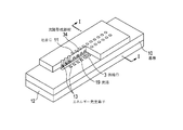
本発明の実施形態の記録ヘッドは、インクを吐出するために用いられるエネルギーを発生するエネルギー発生素子13が所定のピッチで形成された基板10を有している。基板10にはインクを供給する供給口3が、エネルギー発生素子13の2つの列の間に開口されている。基板上には、流路形成部材34によって、各エネルギー発生素子の上方に開口する吐出口11と、供給口3から各吐出口11に連通する個別のインクの流路19が形成されている。吐出口11は、エネルギー発生素子13に対応して設けられている。
The recording head according to the embodiment of the present invention includes a
この記録ヘッドは、吐出口11が形成された面が記録媒体の記録面に対面するように配置される。そしてこの記録ヘッドは、インク供給口3を介して流路内に充填されたインクに、エネルギー発生素子13によって発生する圧力を加えることによって、吐出口11からインク液滴を吐出させ、これを記録媒体に付着させることによって記録を行う。
This recording head is arranged so that the surface on which the
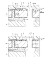
次いで本発明による記録ヘッドの構造の特徴について図2を参照して詳しく説明する。 Next, the characteristics of the structure of the recording head according to the present invention will be described in detail with reference to FIG.
図2は、本発明の第1の実施形態に係る記録ヘッドの模式的断面図であり、図1におけるA−A’を通り基板に垂直な面の位置を部分的に見た図である。 FIG. 2 is a schematic cross-sectional view of the recording head according to the first embodiment of the present invention, and is a view partially showing the position of a plane passing through A-A ′ in FIG. 1 and perpendicular to the substrate.
図示されている記録ヘッドには、後述する駆動回路31に電気的に接続された貫通電極1と、被覆膜2が形成された供給口3とが設けられている。もっとも、貫通電極のみを有する半導体デバイスでも、保護層が形成された供給口のみを有する記録ヘッドでもそれぞれの部分を抽出すれば構造は同じである。尚、図中の符号10は、基板(基板)を示している。以下同様に、符号11は吐出口、符号12は支持部材としてのチッププレートを示している。また基板の一方の面にはエネルギー発生素子13と、エネルギー発生素子の保護層としても機能するパッシベイション層15、層間絶縁層32が設けられている。また、符号31はエネルギー発生素子を駆動するための信号を伝達する駆動回路、符号16はバリア層、符号17は貫通電極と基板との間に設けられた絶縁膜、符号18はへこみ部をそれぞれ示している。被覆膜2と絶縁膜17は共通した材料で形成されている。被覆膜2と絶縁膜17の材料としては、ポリパラキシリレン樹脂、ポリ尿素樹脂、ポリイミド樹脂、酸化シリコン膜等を選択することができる。とりわけポリパラキシリレンはインクに対する耐性が強く好適である。
The illustrated recording head is provided with a through electrode 1 electrically connected to a
また、被覆膜2、絶縁膜17は、基板に設けられたへこみ部18にならう形で設けられているとともに、基板の一方の面で層間絶縁層32に覆われている。このようにすることで、被覆膜2は、より基板10から剥離しにくい構成となっている。
The covering
パッシベイション層15としてはSiNが、層間絶縁層32としてはSiO2などが用いられる。これらは以下に示す実施形態にも適用できる。また、被覆膜、絶縁膜は、基板の一方の面の裏面である他方の面を被覆するように設けられている。また裏面側では、チッププレート12と、基板10が封止剤を介して接合されている。
SiN is used as the
以下に示す実施形態も、従来に比べて被覆膜2、絶縁膜17の基板との剥離が抑制された構成である。
The embodiment described below also has a configuration in which peeling of the
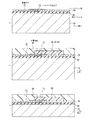
(第2の実施形態)
図3は、本発明の第2の実施形態である記録ヘッドの模式的断面図であり、図2と同様の断面でみたものである。具体的には、被覆膜2は、層間絶縁層32の側面とも接している。よって、層間絶縁層32と被覆膜2とが接する距離、面積が、図2に示す記録ヘッドよりも大きく、よりシール性が高い構造を備えた記録ヘッドを示している。
(Second Embodiment)
FIG. 3 is a schematic cross-sectional view of a recording head according to the second embodiment of the present invention, and is a cross-sectional view similar to FIG. Specifically, the
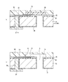
(第3の実施形態)
図4は、本発明の第3の実施形態である記録ヘッドの模式的断面図であり、図2と同様の断面でみたものである。具体的には、パッシベイション層15と基板10との間に絶縁膜17、被覆膜2が挟まれるように構成された記録ヘッドを示している。図4に示されている構造の記録ヘッドは、より絶縁膜17、被覆膜2が剥れ難く、インクが基板まで到達しにくい。また絶縁膜17は、駆動回路31とパッシベイション層15に覆われている。
(Third embodiment)
FIG. 4 is a schematic cross-sectional view of a recording head according to the third embodiment of the present invention, and is a cross-sectional view similar to FIG. Specifically, the recording head is configured so that the insulating
(第4の実施形態)
図5は、本発明の第4の実施形態である記録ヘッドの模式的断面図であり、図2と同様の断面でみたものである。具体的には、2つの機能層(ここでは、素子分離に用いる熱酸化膜21と、配線間の絶縁に用いられる層間絶縁層22との間に絶縁膜17、被覆膜2が挟まれるように構成された記録ヘッドを示している。
(Fourth embodiment)
FIG. 5 is a schematic cross-sectional view of a recording head according to the fourth embodiment of the present invention, and is a cross-sectional view similar to FIG. Specifically, the insulating
(第5の実施形態)
図6(a)及び図6(b)は、本発明の第5の実施形態である記録ヘッドの模式的断面図であり、図2と同様の断面でみたものである。具体的には、2つの機能層(ここでは、パッシベイション層15と層間絶縁層の酸化膜32)の間に絶縁膜17、被覆膜2が挟まれるように構成された記録ヘッドを示している。また、絶縁膜17の一部は、配線18に被覆されている。
(Fifth embodiment)
FIGS. 6A and 6B are schematic cross-sectional views of a recording head according to the fifth embodiment of the present invention, and are seen in the same cross section as FIG. Specifically, the recording head is configured such that the insulating
また、図10(b)において、破線枠箇所に示されるように、パッシベイション層15の供給口側の端部が、供給口の内壁面よりも、供給口から遠く離れ後退した位置をとることもできる。このような構成にすると、被覆膜2に応力が発生した場合にさらに有効であると考えられる。すなわち、被覆膜2の主な引っ張り応力は、側壁にそった方向であり、基板表面にほぼ垂直な方向である。パッシベイション層15は、被覆膜2の側壁に沿う軸からずれた位置に形成されるため、被覆膜2の応力がパッシベイション層15へ与える影響が低減されていると考えられる。そのため、被覆膜2との密着性がさらに向上され、パッシベイション層15と被覆膜2との界面から、インクがより侵入しにくくなっていると考えられる。
10B, the end of the
(第6の実施形態)
図7(a)及び図7(b)は、本発明の第6の実施形態である記録ヘッドの模式的断面図であり、図2と同様の断面でみたものである。パッシベイション層15と層間絶縁層の酸化シリコン膜32との間および基板10とパッシベイション層15との間に、絶縁膜17、被覆膜2が挟まれるように構成された記録ヘッドを示している。本実施形態ではへこみ部は機能層の一部が後退しているのと共に、機能層同士の間にも空間があり、そこに絶縁膜17、被覆膜2が入り込んでいる。
(Sixth embodiment)
FIG. 7A and FIG. 7B are schematic cross-sectional views of a recording head according to the sixth embodiment of the present invention, and are seen in the same cross section as FIG. A recording head configured such that the insulating
また、図7(b)に示す形態は、図6(b)に示したものと同様に、パッシベイション層15の供給口側の端部は、供給口の側壁部分よりも、供給口から遠い位置とした形態である。こちらについても、第5の実施形態を用いて説明したようにパッシベイション層15と、被覆膜2との密着性がさらに向上されていると考えられる。
Further, in the form shown in FIG. 7B, the end on the supply port side of the
(第7の実施形態)
次に、本発明の第7の実施形態としての記録ヘッドの製造方法について具体的に説明する。図2で示した形態の記録ヘッドの製造方法について説明する。
(Seventh embodiment)
Next, a manufacturing method of a recording head as a seventh embodiment of the present invention will be specifically described. A method of manufacturing the recording head having the form shown in FIG. 2 will be described.
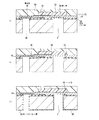
図8〜図10は、本実施形態の記録ヘッドの製造方法の一例を示す模式的断面図である。 8 to 10 are schematic cross-sectional views illustrating an example of a method for manufacturing a recording head according to the present embodiment.
図8(a)に示すように、単結晶のシリコン基板10上に、エネルギー発生素子13とその駆動回路31および駆動回路31の絶縁層であって、エッチングストップ層としても機能する酸化シリコン膜32を汎用の半導体工程により形成する。エネルギー発生素子を被覆するように、窒化シリコンによりパッシベイション層15を形成する。
As shown in FIG. 8A, an
次に、密着層としてポリエーテルアミド樹脂(図示しない)を塗布、ベークした後に、ノボラック系フォトレジストを塗布する。 Next, after applying and baking a polyetheramide resin (not shown) as an adhesion layer, a novolac photoresist is applied.
その後、フォトリソ技術でレジストをパターニングした後に、CF4とO2によるケミカルドライエッチングにより、少なくともエネルギー発生素子13上と、外部電極接続用パッド上と、供給口形成位置のポリアミド樹脂を除去する。次いで、レジストをモノアミン系剥離液により除去する。
Thereafter, after patterning the resist by photolithography, at least the
次いで、図8(b)に示すように、シリコン基板10上に、ポリメチルイソプロペニルケトンをスピンコートし、120℃で20分間プリベークする。その後、UV光により露光を行い、メチルイソブチルケトン/キシレン=2/1を用いて現像し、キシレンでリンスする。以上によって、シリコン基板10上に、溶解可能な樹脂層33を形成する。この樹脂層33は、図2に示す供給口3とエネルギー発生素子13との間のインク流路19を確保するためのものである。
Next, as shown in FIG. 8B, polymethylisopropenyl ketone is spin-coated on the
次いで、被覆樹脂34であるカチオン重合型エポキシ樹脂を塗布し、感光性を有する撥水剤を重ねて塗布し、これにフォトリソ技術により吐出口11を形成する。吐出口はこの時点で形成してもよいし、後に形成する工程を行ってもよい。
Next, a cationic polymerization type epoxy resin which is the
その後、図8(c)に示すように、被覆樹脂34を保護するためのサポート基板(図示しない)をロウにより貼り付け、バックグラインドによりシリコン基板10を研磨して薄くし、次いで希フッ酸により破砕層除去を行い、テープを剥離する。
After that, as shown in FIG. 8C, a support substrate (not shown) for protecting the
次に、シリコン基板10の裏面にノボラック系レジストを塗布し、フォトリソ工程によって、図2に示す貫通電極1用の貫通口と、供給口3とが形成される位置を除去するようにパターニングする(不図示)。
Next, a novolac resist is applied to the back surface of the
その後、シリコン基板10の裏面からICP-RIEエッチャーにより、表面のエッチングストップ層(酸化シリコン膜)32までエッチングを行い、図9(a)に示すように、貫通口35と供給口3とを形成する。次いで、さらにエッチング処理を継続し、ノッチング現象により基板10上の機能層(ここでは、エッチングストップ層32)と接する部分を側方にエッチングし、へこみ部18を形成する。このへこみ部18の形成方法は、ノッチング現象に限定されない。
Thereafter, etching is performed from the back surface of the
次に、図9(b)に示すように、図2に示す絶縁膜17及び被覆膜2となるポリパラキシリレン膜36をCVDにより成膜する。このとき、ポリパラキシリレン膜36は貫通口35と供給口3の内壁を被覆する。その後、シリコン基板10の裏面にドライフィルムによってレジストを成膜し、露光を行なってから供給口3の部分のレジストを除去する。次いで、RIEによって貫通口35および供給口3の内壁を覆うポリパラキシリレン36のうち、基板表面側で層間絶縁層32と接する部分の一部をエッチング除去する。その後、シリコン基板10の裏面のレジストを除去する。
Next, as shown in FIG. 9B, the
また、ポリパラキシリレン樹脂の中で特に、ポリテトラフルオロパラキシリレン樹脂を用いた場合には、シリコン基板10への付着速度を考え、シリコン基板10を冷却しながら成膜させることが好適である。
Further, in particular, when a polytetrafluoroparaxylylene resin is used among the polyparaxylylene resins, it is preferable to form the film while cooling the
次に、図9(c)に示すように、貫通口35および供給口3の底部に露出した絶縁層であるエッチングストップ層(酸化シリコン膜)32をRIEにより除去してから、シリコン基板10の裏面に、めっきの下敷層となる金をスパッタする。次いで、感光性ドライフィルムをシリコン基板10の裏面に貼り付け、導電層を形成しない領域をマスクするようにフォトリソ技術によりパターニングする。その後、下敷層に電位を印加し、貫通導電層および裏面導電層となる金37をめっきにより成膜する。さらに、ドライフィルムを剥離し、めっきが存在しない領域の下敷層を除去する。
Next, as shown in FIG. 9C, the etching stop layer (silicon oxide film) 32, which is an insulating layer exposed at the bottom of the through
その後、図10に示すように、CDEによって、供給口3の底部のパッシベイション層15を除去した後、シリコン基板10を乳酸メチルに浸漬し、溶出可能な樹脂層33を除去する。
Thereafter, as shown in FIG. 10, after the
ロウが溶融する温度までシリコン基板10を加熱し、サポート基板を剥離した後、ダイサーにより基板を切断してチップ化する。これをチッププレートに貼り付けるとともに、外部電極と貫通電極1とを接続するなどしてカートリッジ形態に組み立てることによって、図2に示す記録ヘッドが完成する。
After the
(第8の実施形態)
本発明の第8の実施形態である記録ヘッドの製造方法について以下に説明する。
(Eighth embodiment)
A method for manufacturing a recording head according to the eighth embodiment of the present invention will be described below.
以下に説明する製法は、図9(a)に示す工程までは、第7の実施形態と同様である。供給口3および、貫通口35の形成において先に述べたノッチング現象を利用してもよいし、利用しなくてもよい。
The manufacturing method described below is the same as that of the seventh embodiment up to the step shown in FIG. In the formation of the
次いで、図11(a)に示すように、貫通口35及び供給口3の基板表面側において露出した層間絶縁層である酸化シリコン膜32をBHFにより除去する。
Next, as shown in FIG. 11A, the
次いで、図11(b)に示すように、酸化シリコン膜32を供給口3、貫通口35後退させるために、所望の時間オーバーエッチングを行い、供給口3の壁面にへこみ部18を形成する。つまり、本実施形態は機能層の一つである絶縁層の酸化シリコン膜32を犠牲層として用いたことになる。
Next, as shown in FIG. 11B, overetching is performed for a desired time in order to retract the
次に、図11(c)に示すように、絶縁層兼保護層となるポリパラキシリレン膜36をCVDにより成膜する。このとき、同時にへこみ部18をポリパラキシリレン膜36によって埋める。
Next, as shown in FIG. 11C, a
その後、シリコン基板10の裏面にドライフィルムによりレジストを成膜し、露光および現像を行って、供給口3部分のレジストを除去する。
Thereafter, a resist is formed on the back surface of the
次いで、RIEによって貫通口35および供給口3の内壁のうち、基板表面側のポリパラキシリレン膜36をエッチング除去した後、裏面のレジストを除去する。
Next, the
次に、図12(a)に示すように、シリコン基板10の裏面に、めっきの下敷層となる金をスパッタし、感光性ドライフィルムを基板裏面に貼り付け、導電層を形成しない領域をマスクするようにフォトリソ技術によりパターニングする。
Next, as shown in FIG. 12 (a), gold as an underlay layer is sputtered on the back surface of the
その後、下敷層に電位を印加し、貫通導電層および裏面導電層となる金37をめっきにより成膜した。次いでドライフィルムを剥離し、めっきが存在しない領域の下敷層を除去する。
Thereafter, a potential was applied to the underlying layer, and
次に、図12(b)に示すように、CDEにより供給口3の基板表面側のパッシベイション層(窒化シリコン膜)15を除去した後、シリコン基板10を乳酸メチルに浸漬し、溶出可能な樹脂層33を除去する。
Next, as shown in FIG. 12B, after removing the passivation layer (silicon nitride film) 15 on the substrate surface side of the
その後、ロウが溶融する温度までシリコン基板10を加熱し、サポート基板を剥離した後、ダイサーによって切断してチップ化する。これをチッププレートに貼り付けると同時に外部電極と裏面導電を接続するなどしてカートリッジ形態に組み立て、図4に示す記録ヘッドが完成する。
Thereafter, the
(第9の実施形態)
本発明の第9の実施形態である記録ヘッドの製造方法について、図13及び図14を用いて説明する。
(Ninth embodiment)
A recording head manufacturing method according to the ninth embodiment of the present invention will be described with reference to FIGS.
本実施形態によると、図6に示した記録ヘッドを得ることができる。まず、先に図8(a)を参照して説明した工程において、酸化シリコン膜32上に、シリコン基板10に対して選択的に除去可能な犠牲層36を形成し、その上に、電極層31およびパッシベイション層15を設ける。その後、図8(b)、図8(c)および図9(a)を参照して説明した工程を行う。さらに、貫通口35及び供給口3の底部において露出した絶縁層である酸化シリコン膜32をRIEにより除去し、犠牲層36の領域内に達する穴を形成して犠牲層36を部分的に露出させる。すると図13(a)に示される状態となる。
According to this embodiment, the recording head shown in FIG. 6 can be obtained. First, in the process described above with reference to FIG. 8A, a
その後、露出した犠牲層36全てを除去し、図13(b)に示される状態を得る。本実施形態では犠牲層の全てを除去するので、保護膜の入り込む範囲を精度良く規定できる。このとき犠牲層は周囲の他の構造よりも早くエッチングされる材料であり、後に成膜される保護層よりも薄く形成できるものであれば何を用いても良い。
Thereafter, all of the exposed
犠牲層にアルミの薄膜を用い、これを燐酸、酢酸、硝酸の混合液により、除去してもよい。このとき貫通電極の形成も行う場合は、犠牲層の上にある電子回路の配線との間にバリアメタルを予め成膜しておくと良い。バリアメタルはチタン、窒化チタン、窒化タンタル等から適宜選択できる。 An aluminum thin film may be used for the sacrificial layer, and this may be removed with a mixed solution of phosphoric acid, acetic acid and nitric acid. In this case, when a through electrode is also formed, a barrier metal is preferably formed in advance between the wiring of the electronic circuit on the sacrificial layer. The barrier metal can be appropriately selected from titanium, titanium nitride, tantalum nitride, and the like.
また、犠牲層にBPSG膜(Boron-doped Phospher-Silicate Glass)を用いても良い。このときの犠牲層の除去は、CF4などのフッ素系ガスを用いたCDE、あるいはBHFを用いることができる。一般的にBPSGのエッチングレートは高いが、同時にエッチャントに触れることになる酸化シリコン膜のエッチングを考慮し、膜厚を設定することが重要である。例えばBPSG膜は6000Å程度で、酸化シリコン膜は7000Å以上に成膜しておくことが望ましい。 Further, a BPSG film (Boron-doped Phospher-Silicate Glass) may be used for the sacrificial layer. At this time, the sacrificial layer can be removed by using CDE using a fluorine-based gas such as CF 4 or BHF. In general, the etching rate of BPSG is high, but it is important to set the film thickness in consideration of the etching of the silicon oxide film that is in contact with the etchant at the same time. For example, it is desirable to form the BPSG film at about 6000 mm and the silicon oxide film at 7000 mm or more.
次に、絶縁膜17兼被覆膜2となるポリパラキシリレン膜36をCVDにより成膜する。このとき、同時にへこみ部18をポリパラキシリレン36によって埋める。その後、シリコン基板10の裏面にドライフィルムによりレジストを成膜し、露光現像を行って、供給口3部分のレジストを除去する。
Next, a
次いで、RIEによって貫通口35および供給口3の底部のポリパラキシリレン膜36をエッチング除去した後、裏面のレジストを除去し、図13(c)に示す状態を得る。
Next, after removing the
次に、シリコン基板10の裏面に、めっきの下敷層となる金をスパッタし、感光性ドライフィルムを基板裏面に貼り付け、導電層を形成しない領域をマスクするようにフォトリソ技術によりパターニングする。その後、下敷層に電位を印加し、貫通導電層1および裏面導電層となる金37をめっきにより成膜した。次いでドライフィルムを剥離し、めっきが存在しない領域の下敷層を除去して、図14(a)の状態を得る。
Next, gold serving as an underlayer for plating is sputtered on the back surface of the
次に、図14(b)に示すように、CDEにより供給口3の底部のパッシベイション層15を除去した後、シリコン基板10を乳酸メチルに浸漬し、溶出可能な樹脂層33を除去する。
Next, as shown in FIG. 14B, after the
その後、ロウが溶融する温度までシリコン基板10を加熱し、サポート基板を剥離した後、ダイサーによって切断してチップ化する。これをチッププレートに貼り付けると同時に外部電極と裏面導電を接続するなどしてカートリッジ形態に組み立て、図6(a)に示す記録ヘッドが完成する。
Thereafter, the
図14(a)に示す工程の後、パッシベイション層15の供給口側の端部を除去し、図14(c)のようにすることができる。除去方法としては、CDE、ウェットエッチング、やドライエッチングなどを選択可能で、パッシベイション層15の材料に応じて選択できる。このとき、パッシベイション層15はサイドエッチングされ、供給口の側面よりも端部の位置が後退する。
After the step shown in FIG. 14A, the end portion on the supply port side of the
その後、図14(b)を参照して説明した工程を同様に行うことにより、図6(b)に示す記録ヘッドを得ることができる。 Thereafter, the process described with reference to FIG. 14B is performed in the same manner, whereby the recording head shown in FIG. 6B can be obtained.
(第10の実施形態)
本発明の第10の実施形態である記録ヘッドの製造方法について、図15を用いて説明する。
(Tenth embodiment)
A manufacturing method for a recording head according to the tenth embodiment of the present invention will be described with reference to FIGS.
図15に示される状態は、以下の点で、図13(a)に示される状態と異なる。すなわち、シリコン基板10上に形成された層間絶縁層の酸化シリコン膜32が、貫通電極、供給口形成位置から後退していること、そして犠牲層36が貫通電極、供給口形成位置から基板へ、そして酸化シリコン膜32上にまで及んでいることが特徴である。その他の点は、第9の実施形態と同様である。図15で示される状態より以降は、第9の実施形態と同様に行って、図7に示される記録ヘッドを得ることができる。
The state shown in FIG. 15 is different from the state shown in FIG. 13A in the following points. That is, the
2 被覆膜
3 供給口
10 基板
11 吐出口
13 エネルギー発生素子
19 流路
32 層間絶縁層
2
Claims (3)
前記エネルギー発生素子に対応して設けられたインクの吐出口と、
前記吐出口に連通するインクの流路と、
前記基板の前記一方の面から前記一方の面の裏面である他方の面までを貫通し、前記流路と連通する供給口と、
前記供給口の内壁を覆う膜と、
を有するインクジェット記録ヘッドであって、
前記膜は、前記一方の面の上にまで設けられ、かつ前記一方の面の上に設けられた層に覆われており、
前記基板はシリコンで形成されており、
前記層は、シリコンの窒化物で形成され、前記エネルギー発生素子を覆う層であり、
前記膜の一部は、前記一方の面に設けられたシリコンの酸化物の層とシリコンの窒化物の前記層とに挟まれている、インクジェット記録ヘッド。 A substrate having, on one side, an energy generating element that generates energy used to eject ink;
An ink ejection port provided corresponding to the energy generating element;
An ink flow path communicating with the ejection port;
A supply port that penetrates from the one surface of the substrate to the other surface that is the back surface of the one surface, and communicates with the flow path;
A film covering the inner wall of the supply port;
An ink jet recording head comprising:
The film is provided up to the one surface and covered with a layer provided on the one surface ;
The substrate is formed of silicon;
The layer is formed of silicon nitride and covers the energy generating element.
An ink jet recording head , wherein a part of the film is sandwiched between a silicon oxide layer and a silicon nitride layer provided on the one surface .
Priority Applications (1)
| Application Number | Priority Date | Filing Date | Title |
|---|---|---|---|
| JP2008002329A JP5043689B2 (en) | 2007-01-09 | 2008-01-09 | Ink jet recording head, manufacturing method thereof, and semiconductor device |
Applications Claiming Priority (5)
| Application Number | Priority Date | Filing Date | Title |
|---|---|---|---|
| JP2007001477 | 2007-01-09 | ||
| JP2007001477 | 2007-01-09 | ||
| JP2007290676 | 2007-11-08 | ||
| JP2007290676 | 2007-11-08 | ||
| JP2008002329A JP5043689B2 (en) | 2007-01-09 | 2008-01-09 | Ink jet recording head, manufacturing method thereof, and semiconductor device |
Publications (3)
| Publication Number | Publication Date |
|---|---|
| JP2009132133A JP2009132133A (en) | 2009-06-18 |
| JP2009132133A5 JP2009132133A5 (en) | 2010-12-02 |
| JP5043689B2 true JP5043689B2 (en) | 2012-10-10 |
Family
ID=39593900
Family Applications (1)
| Application Number | Title | Priority Date | Filing Date |
|---|---|---|---|
| JP2008002329A Active JP5043689B2 (en) | 2007-01-09 | 2008-01-09 | Ink jet recording head, manufacturing method thereof, and semiconductor device |
Country Status (2)
| Country | Link |
|---|---|
| US (1) | US7926909B2 (en) |
| JP (1) | JP5043689B2 (en) |
Families Citing this family (14)
| Publication number | Priority date | Publication date | Assignee | Title |
|---|---|---|---|---|
| JP5606213B2 (en) * | 2009-09-04 | 2014-10-15 | キヤノン株式会社 | Manufacturing method of substrate for liquid discharge head |
| JP5701014B2 (en) * | 2010-11-05 | 2015-04-15 | キヤノン株式会社 | Method for manufacturing ejection element substrate |
| WO2013191677A1 (en) * | 2012-06-18 | 2013-12-27 | Hewlett-Packard Development Company, L.P. | Controlling adhesives between substrates and carriers |
| JP5959979B2 (en) * | 2012-08-01 | 2016-08-02 | キヤノン株式会社 | Substrate having through-hole, substrate for liquid discharge head, and method for manufacturing liquid discharge head |
| US9573369B2 (en) | 2012-09-19 | 2017-02-21 | Hewlett-Packard Development Company, L.P. | Fluid ejection assembly with controlled adhesive bond |
| WO2015116050A1 (en) * | 2014-01-29 | 2015-08-06 | Hewlett-Packard Development Company, L.P. | Thermal ink jet printhead |
| JP2018083385A (en) * | 2016-11-25 | 2018-05-31 | キヤノン株式会社 | Method for forming film |
| JP7037334B2 (en) * | 2017-02-17 | 2022-03-16 | キヤノン株式会社 | Substrate for liquid discharge head, its manufacturing method, liquid discharge head and liquid discharge device |
| WO2018150830A1 (en) | 2017-02-17 | 2018-08-23 | Canon Kabushiki Kaisha | Liquid discharge head substrate, method of manufacturing the same, liquid discharge head, and liquid discharge apparatus |
| JP6942537B2 (en) * | 2017-06-29 | 2021-09-29 | キヤノン株式会社 | Liquid discharge head |
| JP7224782B2 (en) * | 2018-05-30 | 2023-02-20 | キヤノン株式会社 | Liquid ejection head and manufacturing method thereof |
| JP7066534B2 (en) * | 2018-06-04 | 2022-05-13 | キヤノン株式会社 | Manufacturing method of liquid discharge head |
| JP7214409B2 (en) * | 2018-09-05 | 2023-01-30 | キヤノン株式会社 | liquid ejection head |
| US11161351B2 (en) * | 2018-09-28 | 2021-11-02 | Canon Kabushiki Kaisha | Liquid ejection head |
Family Cites Families (7)
| Publication number | Priority date | Publication date | Assignee | Title |
|---|---|---|---|---|
| JP3227285B2 (en) * | 1993-09-17 | 2001-11-12 | シチズン時計株式会社 | Method of manufacturing inkjet head |
| JPH0911478A (en) | 1995-06-27 | 1997-01-14 | Canon Inc | Method of manufacturing ink jet recording head |
| JP2001162803A (en) * | 1999-12-10 | 2001-06-19 | Casio Comput Co Ltd | Monolithic inkjet printer head |
| JP3726909B2 (en) * | 2002-07-10 | 2005-12-14 | セイコーエプソン株式会社 | Method for manufacturing liquid jet head |
| US7377625B2 (en) * | 2004-06-25 | 2008-05-27 | Canon Kabushiki Kaisha | Method for producing ink-jet recording head having filter, ink-jet recording head, substrate for recording head, and ink-jet cartridge |
| JP2006310499A (en) * | 2005-04-27 | 2006-11-09 | Konica Minolta Holdings Inc | Wiring board, piezoelectric ceramic element and their manufacturing methods |
| JP4766658B2 (en) * | 2005-05-10 | 2011-09-07 | キヤノン株式会社 | Liquid discharge head and manufacturing method thereof |
-
2008
- 2008-01-07 US US11/970,396 patent/US7926909B2/en not_active Expired - Fee Related
- 2008-01-09 JP JP2008002329A patent/JP5043689B2/en active Active
Also Published As
| Publication number | Publication date |
|---|---|
| US7926909B2 (en) | 2011-04-19 |
| US20080165222A1 (en) | 2008-07-10 |
| JP2009132133A (en) | 2009-06-18 |
Similar Documents
| Publication | Publication Date | Title |
|---|---|---|
| JP5043689B2 (en) | Ink jet recording head, manufacturing method thereof, and semiconductor device | |
| JP5361231B2 (en) | Ink jet recording head and electronic device | |
| EP1923219B1 (en) | Inkjet head | |
| US8037603B2 (en) | Ink jet head and producing method therefor | |
| US7918544B2 (en) | Inkjet head | |
| US20080227035A1 (en) | Method of producing an ink jet head and method of producing an electronic device | |
| US8733900B2 (en) | Thermal inkjet print head with solvent resistance | |
| JP2008179045A (en) | Ink jet recording head and manufacturing method thereof, semiconductor device and manufacturing method thereof | |
| US6953530B2 (en) | Forming method of ink jet print head substrate and ink jet print head substrate, and manufacturing method of ink jet print head and ink jet print head | |
| JP6029316B2 (en) | Method for manufacturing liquid discharge head | |
| JP4979793B2 (en) | Manufacturing method of substrate for liquid discharge head | |
| JP2000334956A (en) | Ink jet printer head and method of manufacturing the same | |
| US7264917B2 (en) | Fluid injection micro device and fabrication method thereof | |
| JP3861532B2 (en) | Inkjet printer head manufacturing method | |
| JP5224782B2 (en) | Method for manufacturing liquid discharge head | |
| JP2007301886A (en) | Ink jet print head and method of manufacturing the same | |
| JP2014188702A (en) | Liquid discharge unit and method of manufacturing liquid discharge unit | |
| JP2004058287A (en) | Liquid ejection head | |
| US20080143791A1 (en) | Liquid jet head chip and manufacturing method therefor | |
| JP2011189597A (en) | Manufacturing method of liquid jet head, liquid jet head and liquid jet apparatus | |
| JP2008200905A (en) | Method for manufacturing liquid jet head | |
| JP2006224591A (en) | Method for manufacturing ink jet recording head |
Legal Events
| Date | Code | Title | Description |
|---|---|---|---|
| A521 | Written amendment |
Free format text: JAPANESE INTERMEDIATE CODE: A523 Effective date: 20101015 |
|
| A621 | Written request for application examination |
Free format text: JAPANESE INTERMEDIATE CODE: A621 Effective date: 20101015 |
|
| A131 | Notification of reasons for refusal |
Free format text: JAPANESE INTERMEDIATE CODE: A131 Effective date: 20120321 |
|
| A977 | Report on retrieval |
Free format text: JAPANESE INTERMEDIATE CODE: A971007 Effective date: 20120321 |
|
| A521 | Written amendment |
Free format text: JAPANESE INTERMEDIATE CODE: A523 Effective date: 20120518 |
|
| TRDD | Decision of grant or rejection written | ||
| A01 | Written decision to grant a patent or to grant a registration (utility model) |
Free format text: JAPANESE INTERMEDIATE CODE: A01 Effective date: 20120612 |
|
| A01 | Written decision to grant a patent or to grant a registration (utility model) |
Free format text: JAPANESE INTERMEDIATE CODE: A01 |
|
| A61 | First payment of annual fees (during grant procedure) |
Free format text: JAPANESE INTERMEDIATE CODE: A61 Effective date: 20120712 |
|
| R151 | Written notification of patent or utility model registration |
Ref document number: 5043689 Country of ref document: JP Free format text: JAPANESE INTERMEDIATE CODE: R151 |
|
| FPAY | Renewal fee payment (event date is renewal date of database) |
Free format text: PAYMENT UNTIL: 20150720 Year of fee payment: 3 |