JP5040977B2 - Nitride semiconductor substrate, semiconductor device and manufacturing method thereof - Google Patents
Nitride semiconductor substrate, semiconductor device and manufacturing method thereof Download PDFInfo
- Publication number
- JP5040977B2 JP5040977B2 JP2009218890A JP2009218890A JP5040977B2 JP 5040977 B2 JP5040977 B2 JP 5040977B2 JP 2009218890 A JP2009218890 A JP 2009218890A JP 2009218890 A JP2009218890 A JP 2009218890A JP 5040977 B2 JP5040977 B2 JP 5040977B2
- Authority
- JP
- Japan
- Prior art keywords
- nitride semiconductor
- semiconductor substrate
- plane
- main surface
- chamfered portion
- Prior art date
- Legal status (The legal status is an assumption and is not a legal conclusion. Google has not performed a legal analysis and makes no representation as to the accuracy of the status listed.)
- Active
Links
- 239000004065 semiconductor Substances 0.000 title claims description 292
- 239000000758 substrate Substances 0.000 title claims description 292
- 150000004767 nitrides Chemical class 0.000 title claims description 231
- 238000004519 manufacturing process Methods 0.000 title claims description 38
- 239000010410 layer Substances 0.000 claims description 111
- 238000000034 method Methods 0.000 claims description 55
- 230000002093 peripheral effect Effects 0.000 claims description 29
- 230000003746 surface roughness Effects 0.000 claims description 16
- 239000002344 surface layer Substances 0.000 claims description 3
- 238000003754 machining Methods 0.000 claims 1
- JMASRVWKEDWRBT-UHFFFAOYSA-N Gallium nitride Chemical compound [Ga]#N JMASRVWKEDWRBT-UHFFFAOYSA-N 0.000 description 42
- 239000013078 crystal Substances 0.000 description 32
- 238000000227 grinding Methods 0.000 description 24
- 238000012545 processing Methods 0.000 description 20
- 238000012986 modification Methods 0.000 description 17
- 230000004048 modification Effects 0.000 description 17
- 238000010586 diagram Methods 0.000 description 16
- 229920001971 elastomer Polymers 0.000 description 15
- 229910002704 AlGaN Inorganic materials 0.000 description 13
- 230000010355 oscillation Effects 0.000 description 12
- 238000012360 testing method Methods 0.000 description 12
- 238000005520 cutting process Methods 0.000 description 11
- 230000000694 effects Effects 0.000 description 10
- 238000005530 etching Methods 0.000 description 9
- 230000007547 defect Effects 0.000 description 7
- 229910003460 diamond Inorganic materials 0.000 description 7
- 239000010432 diamond Substances 0.000 description 7
- 238000002248 hydride vapour-phase epitaxy Methods 0.000 description 7
- 239000010936 titanium Substances 0.000 description 7
- 238000005336 cracking Methods 0.000 description 6
- 239000010931 gold Substances 0.000 description 6
- 239000012535 impurity Substances 0.000 description 6
- 239000000203 mixture Substances 0.000 description 6
- 238000005498 polishing Methods 0.000 description 6
- 238000002360 preparation method Methods 0.000 description 6
- 238000005253 cladding Methods 0.000 description 5
- 238000007716 flux method Methods 0.000 description 5
- PXHVJJICTQNCMI-UHFFFAOYSA-N Nickel Chemical compound [Ni] PXHVJJICTQNCMI-UHFFFAOYSA-N 0.000 description 4
- 238000003776 cleavage reaction Methods 0.000 description 4
- 229910052751 metal Inorganic materials 0.000 description 4
- 239000002184 metal Substances 0.000 description 4
- 239000002245 particle Substances 0.000 description 4
- 230000007017 scission Effects 0.000 description 4
- XUIMIQQOPSSXEZ-UHFFFAOYSA-N Silicon Chemical compound [Si] XUIMIQQOPSSXEZ-UHFFFAOYSA-N 0.000 description 3
- 230000015572 biosynthetic process Effects 0.000 description 3
- 230000007423 decrease Effects 0.000 description 3
- 238000002474 experimental method Methods 0.000 description 3
- 239000011777 magnesium Substances 0.000 description 3
- 239000000463 material Substances 0.000 description 3
- 229910052710 silicon Inorganic materials 0.000 description 3
- 239000010703 silicon Substances 0.000 description 3
- QGZKDVFQNNGYKY-UHFFFAOYSA-N Ammonia Chemical compound N QGZKDVFQNNGYKY-UHFFFAOYSA-N 0.000 description 2
- FYYHWMGAXLPEAU-UHFFFAOYSA-N Magnesium Chemical compound [Mg] FYYHWMGAXLPEAU-UHFFFAOYSA-N 0.000 description 2
- 229910004298 SiO 2 Inorganic materials 0.000 description 2
- GWEVSGVZZGPLCZ-UHFFFAOYSA-N Titan oxide Chemical compound O=[Ti]=O GWEVSGVZZGPLCZ-UHFFFAOYSA-N 0.000 description 2
- RTAQQCXQSZGOHL-UHFFFAOYSA-N Titanium Chemical compound [Ti] RTAQQCXQSZGOHL-UHFFFAOYSA-N 0.000 description 2
- 239000006061 abrasive grain Substances 0.000 description 2
- 238000005229 chemical vapour deposition Methods 0.000 description 2
- 230000002950 deficient Effects 0.000 description 2
- 238000013461 design Methods 0.000 description 2
- 239000002019 doping agent Substances 0.000 description 2
- PCHJSUWPFVWCPO-UHFFFAOYSA-N gold Chemical compound [Au] PCHJSUWPFVWCPO-UHFFFAOYSA-N 0.000 description 2
- 229910052737 gold Inorganic materials 0.000 description 2
- 230000017525 heat dissipation Effects 0.000 description 2
- 229910052749 magnesium Inorganic materials 0.000 description 2
- 229920001084 poly(chloroprene) Polymers 0.000 description 2
- 238000002310 reflectometry Methods 0.000 description 2
- 238000011160 research Methods 0.000 description 2
- 229910000679 solder Inorganic materials 0.000 description 2
- 239000004575 stone Substances 0.000 description 2
- 229910052719 titanium Inorganic materials 0.000 description 2
- JLTRXTDYQLMHGR-UHFFFAOYSA-N trimethylaluminium Chemical compound C[Al](C)C JLTRXTDYQLMHGR-UHFFFAOYSA-N 0.000 description 2
- XCZXGTMEAKBVPV-UHFFFAOYSA-N trimethylgallium Chemical compound C[Ga](C)C XCZXGTMEAKBVPV-UHFFFAOYSA-N 0.000 description 2
- IBEFSUTVZWZJEL-UHFFFAOYSA-N trimethylindium Chemical compound C[In](C)C IBEFSUTVZWZJEL-UHFFFAOYSA-N 0.000 description 2
- 238000007740 vapor deposition Methods 0.000 description 2
- 238000000927 vapour-phase epitaxy Methods 0.000 description 2
- 238000001039 wet etching Methods 0.000 description 2
- JBRZTFJDHDCESZ-UHFFFAOYSA-N AsGa Chemical compound [As]#[Ga] JBRZTFJDHDCESZ-UHFFFAOYSA-N 0.000 description 1
- BLRPTPMANUNPDV-UHFFFAOYSA-N Silane Chemical compound [SiH4] BLRPTPMANUNPDV-UHFFFAOYSA-N 0.000 description 1
- VYPSYNLAJGMNEJ-UHFFFAOYSA-N Silicium dioxide Chemical compound O=[Si]=O VYPSYNLAJGMNEJ-UHFFFAOYSA-N 0.000 description 1
- 229910010413 TiO 2 Inorganic materials 0.000 description 1
- XLOMVQKBTHCTTD-UHFFFAOYSA-N Zinc monoxide Chemical compound [Zn]=O XLOMVQKBTHCTTD-UHFFFAOYSA-N 0.000 description 1
- 229910052782 aluminium Inorganic materials 0.000 description 1
- XAGFODPZIPBFFR-UHFFFAOYSA-N aluminium Chemical compound [Al] XAGFODPZIPBFFR-UHFFFAOYSA-N 0.000 description 1
- 229910021529 ammonia Inorganic materials 0.000 description 1
- QVGXLLKOCUKJST-UHFFFAOYSA-N atomic oxygen Chemical compound [O] QVGXLLKOCUKJST-UHFFFAOYSA-N 0.000 description 1
- 230000005540 biological transmission Effects 0.000 description 1
- 238000012790 confirmation Methods 0.000 description 1
- 238000000151 deposition Methods 0.000 description 1
- 230000008021 deposition Effects 0.000 description 1
- 238000002050 diffraction method Methods 0.000 description 1
- 238000005553 drilling Methods 0.000 description 1
- 238000001312 dry etching Methods 0.000 description 1
- 238000000407 epitaxy Methods 0.000 description 1
- -1 for example Substances 0.000 description 1
- 238000010348 incorporation Methods 0.000 description 1
- 238000002347 injection Methods 0.000 description 1
- 239000007924 injection Substances 0.000 description 1
- 229910052742 iron Inorganic materials 0.000 description 1
- 230000001678 irradiating effect Effects 0.000 description 1
- 238000010030 laminating Methods 0.000 description 1
- 238000004943 liquid phase epitaxy Methods 0.000 description 1
- 238000005259 measurement Methods 0.000 description 1
- 229910052759 nickel Inorganic materials 0.000 description 1
- 230000003287 optical effect Effects 0.000 description 1
- TWNQGVIAIRXVLR-UHFFFAOYSA-N oxo(oxoalumanyloxy)alumane Chemical compound O=[Al]O[Al]=O TWNQGVIAIRXVLR-UHFFFAOYSA-N 0.000 description 1
- 229910052760 oxygen Inorganic materials 0.000 description 1
- 239000001301 oxygen Substances 0.000 description 1
- 238000000206 photolithography Methods 0.000 description 1
- 238000007517 polishing process Methods 0.000 description 1
- 238000003825 pressing Methods 0.000 description 1
- 239000002994 raw material Substances 0.000 description 1
- 239000011347 resin Substances 0.000 description 1
- 229920005989 resin Polymers 0.000 description 1
- 238000007790 scraping Methods 0.000 description 1
- 238000000926 separation method Methods 0.000 description 1
- 229910000077 silane Inorganic materials 0.000 description 1
- HBMJWWWQQXIZIP-UHFFFAOYSA-N silicon carbide Chemical compound [Si+]#[C-] HBMJWWWQQXIZIP-UHFFFAOYSA-N 0.000 description 1
- 229910052814 silicon oxide Inorganic materials 0.000 description 1
- 239000002002 slurry Substances 0.000 description 1
- 238000005092 sublimation method Methods 0.000 description 1
- 239000000126 substance Substances 0.000 description 1
- 239000004408 titanium dioxide Substances 0.000 description 1
- 238000001771 vacuum deposition Methods 0.000 description 1
- 238000001947 vapour-phase growth Methods 0.000 description 1
- 230000000007 visual effect Effects 0.000 description 1
- XLYOFNOQVPJJNP-UHFFFAOYSA-N water Substances O XLYOFNOQVPJJNP-UHFFFAOYSA-N 0.000 description 1
Images


Classifications
-
- H—ELECTRICITY
- H01—ELECTRIC ELEMENTS
- H01L—SEMICONDUCTOR DEVICES NOT COVERED BY CLASS H10
- H01L21/00—Processes or apparatus adapted for the manufacture or treatment of semiconductor or solid state devices or of parts thereof
- H01L21/02—Manufacture or treatment of semiconductor devices or of parts thereof
- H01L21/02002—Preparing wafers
- H01L21/02005—Preparing bulk and homogeneous wafers
- H01L21/02008—Multistep processes
- H01L21/0201—Specific process step
- H01L21/02021—Edge treatment, chamfering
-
- C—CHEMISTRY; METALLURGY
- C30—CRYSTAL GROWTH
- C30B—SINGLE-CRYSTAL GROWTH; UNIDIRECTIONAL SOLIDIFICATION OF EUTECTIC MATERIAL OR UNIDIRECTIONAL DEMIXING OF EUTECTOID MATERIAL; REFINING BY ZONE-MELTING OF MATERIAL; PRODUCTION OF A HOMOGENEOUS POLYCRYSTALLINE MATERIAL WITH DEFINED STRUCTURE; SINGLE CRYSTALS OR HOMOGENEOUS POLYCRYSTALLINE MATERIAL WITH DEFINED STRUCTURE; AFTER-TREATMENT OF SINGLE CRYSTALS OR A HOMOGENEOUS POLYCRYSTALLINE MATERIAL WITH DEFINED STRUCTURE; APPARATUS THEREFOR
- C30B29/00—Single crystals or homogeneous polycrystalline material with defined structure characterised by the material or by their shape
- C30B29/10—Inorganic compounds or compositions
- C30B29/40—AIIIBV compounds wherein A is B, Al, Ga, In or Tl and B is N, P, As, Sb or Bi
- C30B29/403—AIII-nitrides
- C30B29/406—Gallium nitride
-
- C—CHEMISTRY; METALLURGY
- C30—CRYSTAL GROWTH
- C30B—SINGLE-CRYSTAL GROWTH; UNIDIRECTIONAL SOLIDIFICATION OF EUTECTIC MATERIAL OR UNIDIRECTIONAL DEMIXING OF EUTECTOID MATERIAL; REFINING BY ZONE-MELTING OF MATERIAL; PRODUCTION OF A HOMOGENEOUS POLYCRYSTALLINE MATERIAL WITH DEFINED STRUCTURE; SINGLE CRYSTALS OR HOMOGENEOUS POLYCRYSTALLINE MATERIAL WITH DEFINED STRUCTURE; AFTER-TREATMENT OF SINGLE CRYSTALS OR A HOMOGENEOUS POLYCRYSTALLINE MATERIAL WITH DEFINED STRUCTURE; APPARATUS THEREFOR
- C30B33/00—After-treatment of single crystals or homogeneous polycrystalline material with defined structure
-
- Y—GENERAL TAGGING OF NEW TECHNOLOGICAL DEVELOPMENTS; GENERAL TAGGING OF CROSS-SECTIONAL TECHNOLOGIES SPANNING OVER SEVERAL SECTIONS OF THE IPC; TECHNICAL SUBJECTS COVERED BY FORMER USPC CROSS-REFERENCE ART COLLECTIONS [XRACs] AND DIGESTS
- Y10—TECHNICAL SUBJECTS COVERED BY FORMER USPC
- Y10T—TECHNICAL SUBJECTS COVERED BY FORMER US CLASSIFICATION
- Y10T83/00—Cutting
- Y10T83/04—Processes
Description
この発明は、窒化物半導体基板、半導体装置およびそれらの製造方法に関し、より特定的には、半極性面である主面を有する窒化物半導体基板、半導体装置およびそれらの製造方法に関する。 The present invention relates to a nitride semiconductor substrate, a semiconductor device, and a manufacturing method thereof, and more particularly to a nitride semiconductor substrate having a main surface that is a semipolar surface, a semiconductor device, and a manufacturing method thereof.
3.4eVのエネルギーバンドギャップおよび高い熱伝導率を有するGaN基板などの窒化物半導体基板は、短波長の光デバイスやパワー電子デバイスなどの半導体装置用の材料として注目されている。このような窒化物半導体基板の一例であるGaN基板においては、基板の欠け、割れなどを防止するために外周端部に面取り加工部を形成することが提案されている(たとえば、特許文献1参照)。 A nitride semiconductor substrate such as a GaN substrate having an energy band gap of 3.4 eV and high thermal conductivity has attracted attention as a material for a semiconductor device such as a short wavelength optical device or a power electronic device. In a GaN substrate which is an example of such a nitride semiconductor substrate, it has been proposed to form a chamfered portion at an outer peripheral end portion in order to prevent chipping or cracking of the substrate (see, for example, Patent Document 1). ).
しかし、上記特許文献1では、基板の主面がc面であり、半極性面である主面(c面から傾斜した主面)を有する窒化物半導体基板については特に言及しておらず、従来そのような半極性面を主面とする窒化物半導体基板の外周端部にどのような面取り加工部を形成すれば、窒化物半導体基板の割れや欠けを効果的に抑制できるのかは知られていなかった。
However, in the above-mentioned
この発明は、上記のような課題を解決するために成されたものであり、この発明の目的は、割れや欠けを効果的に防止することができる面取り加工部を備えた、半極性面である主面を有する窒化物半導体基板、当該窒化物半導体基板を用いた半導体装置、およびそれらの製造方法を提供することである。 This invention is made in order to solve the above problems, and the object of this invention is a semipolar surface provided with a chamfered portion that can effectively prevent cracking and chipping. It is an object to provide a nitride semiconductor substrate having a certain main surface, a semiconductor device using the nitride semiconductor substrate, and a method for manufacturing them.
本発明者は、鋭意研究の結果、半導体レーザを作製したときに発振歩留まりを向上できる窒化物半導体基板は、(0001)面から[1−100]方向に71°以上79°以下傾斜した主面、或いは(000−1)面から[−1100]方向に71°以上79°以下傾斜した主面を有することを見出した。そして、この主面を有する窒化物半導体基板を半導体装置に用いるため、半導体装置の製造工程中や窒化物半導体基板のハンドリング中に当該窒化物半導体基板に割れや欠けが発生することを効果的に抑制することが可能な面取り加工部の形状を見出した。 As a result of diligent research, the inventor has found that a nitride semiconductor substrate capable of improving the oscillation yield when a semiconductor laser is manufactured is a main surface inclined from 71 ° to 79 ° in the [1-100] direction from the (0001) plane. Alternatively, the present inventors have found that the main surface is inclined from 71 ° to 79 ° in the [−1100] direction from the (000-1) plane. Since the nitride semiconductor substrate having this main surface is used for a semiconductor device, it is effective that the nitride semiconductor substrate is cracked or chipped during the manufacturing process of the semiconductor device or during the handling of the nitride semiconductor substrate. The shape of the chamfered part which can be suppressed was found.
すなわち、本発明に従った窒化物半導体基板は、(0001)面から[1−100]方向に71°以上79°以下傾斜した主面、或いは(000−1)面から[−1100]方向に71°以上79°以下傾斜した主面と、主面の外周端部に位置する面取り加工部とを備える。面取り加工部の、主面および当該主面と反対側に位置する裏面のうちのいずれか隣接する一方に対する傾斜角度は5°以上45°以下である。 That is, the nitride semiconductor substrate according to the present invention has a main surface inclined from 71 ° to 79 ° in the [1-100] direction from the (0001) plane, or from the (000-1) plane in the [−1100] direction. A main surface inclined by 71 ° or more and 79 ° or less and a chamfered portion positioned at an outer peripheral end of the main surface are provided. The inclination angle of the chamfered portion with respect to one of the main surface and the back surface located on the opposite side of the main surface is not less than 5 ° and not more than 45 ° .
本発明の窒化物半導体基板によれば、半導体装置を作製したときに歩留りを向上できる主面を有している。さらに、窒化物半導体基板の外周端部からの割れや欠けの発生を抑制することができる。この結果、当該割れや欠けに起因する窒化物半導体基板の不良発生を抑制でき、当該窒化物半導体基板の歩留りを向上させることができる。 The nitride semiconductor substrate of the present invention has a main surface that can improve yield when a semiconductor device is manufactured. Furthermore, generation | occurrence | production of the crack and chip | tip from the outer peripheral edge part of a nitride semiconductor substrate can be suppressed. As a result, the occurrence of defects in the nitride semiconductor substrate due to the cracks and chips can be suppressed, and the yield of the nitride semiconductor substrate can be improved.
この発明に従った窒化物半導体基板の製造方法は、(0001)面から[1−100]方向に71°以上79°以下傾斜した主面、或いは(000−1)面から[−1100]方向に71°以上79°以下傾斜した主面を有する窒化物半導体基板を準備する工程と、窒化物半導体基板の主面の外周端部に面取り加工を施す工程とを備える。面取り加工を施す工程では、主面および主面と反対側に位置する裏面のうちのいずれか隣接する一方に対する傾斜角度が5°以上45°以下となる面取り加工部を形成する。 The method of manufacturing a nitride semiconductor substrate according to the present invention includes a main surface inclined from 71 ° to 79 ° in the [1-100] direction from the (0001) plane, or the [−1100] direction from the (000-1) plane. And a step of preparing a nitride semiconductor substrate having a main surface inclined by 71 ° or more and 79 ° or less and a step of chamfering the outer peripheral end of the main surface of the nitride semiconductor substrate. In the step of performing chamfering, a chamfered portion is formed in which the inclination angle with respect to either the main surface or the back surface located on the opposite side of the main surface is 5 ° or more and 45 ° or less .
このようにすれば、本発明に従った窒化物半導体基板を製造することができる。
この発明に従った半導体装置は、上記窒化物半導体基板を用いた半導体装置である。この場合、窒化物半導体基板の割れや欠けが効果的に抑制されることから、製造歩留りの高い半導体装置を実現できる。
In this way, the nitride semiconductor substrate according to the present invention can be manufactured.
A semiconductor device according to the present invention is a semiconductor device using the nitride semiconductor substrate. In this case, since the cracks and chips of the nitride semiconductor substrate are effectively suppressed, a semiconductor device with a high manufacturing yield can be realized.
この発明に従った半導体装置の製造方法は、上記窒化物半導体基板の製造方法を用いて窒化物半導体基板を準備する工程と、窒化物半導体基板の主面上にエピタキシャル層を形成する工程とを備える。この場合、窒化物半導体基板の割れや欠けが効果的に抑制されることから、半導体装置の高い製造歩留りを実現できる。 A method of manufacturing a semiconductor device according to the present invention includes a step of preparing a nitride semiconductor substrate using the method of manufacturing a nitride semiconductor substrate, and a step of forming an epitaxial layer on a main surface of the nitride semiconductor substrate. Prepare. In this case, since the nitride semiconductor substrate is effectively prevented from being cracked or chipped, a high manufacturing yield of the semiconductor device can be realized.
本発明によれば、窒化物半導体基板の割れや欠けを効果的に抑制でき、結果的に歩留りの高い半導体装置を製造できる。 According to the present invention, it is possible to effectively suppress cracking and chipping of the nitride semiconductor substrate, and as a result, it is possible to manufacture a semiconductor device with a high yield.
以下、図面に基づいて本発明の実施の形態を説明する。なお、以下の図面において同一または相当する部分には同一の参照番号を付し、その説明は繰返さない。また、本明細書中においては、個別方位を[]、個別面を()でそれぞれ示している。また、負の指数については、結晶学上、”−”(バー)を数字の上に付けることになっているが、本明細書中では、数字の前に負の符号を付けている。また、記載の特定方位、方向はそれだけを示すのではなく、当然ながらそれと等価な関係の方位、方向も含むのは言うまでもない。 Hereinafter, embodiments of the present invention will be described with reference to the drawings. In the following drawings, the same or corresponding parts are denoted by the same reference numerals, and description thereof will not be repeated. In the present specification, individual orientations are indicated by [] and individual planes are indicated by (). As for the negative index, “−” (bar) is attached on the number in crystallography, but in this specification, a negative sign is attached before the number. In addition, it is needless to say that the specific azimuth and direction described are not only those but also include the azimuth and direction of the equivalent relationship.
(実施の形態1)
図1〜図3を参照して、本発明による窒化物半導体基板の実施の形態1を説明する。
(Embodiment 1)
A first embodiment of a nitride semiconductor substrate according to the present invention will be described with reference to FIGS.
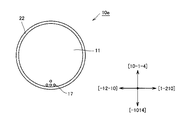
図1および図2に示すように、本発明による窒化物半導体基板10aは、平面形状がほぼ円形状であって、外周端部の一部が直線状に加工されたオリエンテーションフラット12(オリフラ12)が形成されている。また、窒化物半導体基板10aの外周端においては、主面11側のチャンファ加工部である表側面取り部22が形成されている。また、主面11と反対側の裏面21の外周部においては、裏面21側のチャンファ加工部である裏側面取り部23が形成されている。そして、窒化物半導体基板10aの外周端部においては、表側面取り部22と裏側面取り部23とを繋ぐように、曲面状の端面24が形成されている。これらの表側面取り部22、裏側面取り部23および端面24から面取り加工部(チャンファ部)が構成されている。表側面取り部22の幅L2は、裏側面取り部23の幅L1よりも大きくなっている。
As shown in FIGS. 1 and 2, the
主面11の延在方向に対して表側面取り部22の延在方向が角度θ2で交差している。また、裏面21の延在方向に対して、裏側面取り部23の延在方向は角度θ1で交差している。角度θ1と角度θ2とは同じであってもよいが異なる値となっていてもよい。そして、表側面取り部22、裏側面取り部23および端面24の表面層には加工変質層25が形成されている。図2からもわかるように、表側面取り部22に形成された加工変質層25の厚みは、裏側面取り部23において形成された加工変質層25の厚みよりも厚くなっている。
The extending direction of the
この主面11は、(0001)(c+面)面から[1−100]方向(m+軸方向)に71°以上79°以下傾斜した面、或いは(000−1)面(c−面)から[−1100](m−軸方向)方向に71°以上79°以下傾斜した面であり、(20−21)面または(−202−1)面であることが好ましい。なお、主面11の面方位は、上述した面方位(20−21)、(−202−1)から所定の角度だけ傾斜していてもよい。
The
ここで、主面11の面方位について、図3を参照して説明する。図3に示すように、主面11は、(0001)面から[1−100]方向(m+軸方向)に角度θ傾いた面である。言い換えると、主面11は、[0001]方向(c軸方向)から[1−100]方向(m軸方向)に角度θ傾いた面である。角度θは71°以上79°以下であり、73°以上77°以下であることが好ましく、74°以上76°以下であることがより好ましい。なお、(20−21)面または(−202−1)面は、(0001)面または(000−1)面から、m+軸、m−軸方向に約75°(=角度θ)傾いた面である。ここでm−軸方向とは[−1100]方向である。
Here, the plane orientation of the
また、上記角度θが71°以上79°以下の場合、この窒化物半導体基板10aを用いて作製した半導体装置(たとえば半導体レーザ)の歩留まりを向上(たとえば50%以上)することができる。角度θが73°以上77°以下の場合、窒化物半導体基板10aを用いて作製した半導体装置(たとえば半導体レーザ)の歩留まりをより向上(たとえば75%以上)することができる。角度θが74°以上76°以下の場合、窒化物半導体基板10aを用いて作製した半導体装置(たとえば半導体レーザ)の歩留まりをより一層向上(たとえば80%以上)することができる。
When the angle θ is 71 ° or more and 79 ° or less, the yield of a semiconductor device (for example, a semiconductor laser) manufactured using the
さらに、上記窒化物半導体基板10aでは、面取り加工部の、主面11および当該主面11と反対側に位置する裏面21のうちのいずれか隣接する一方に対する傾斜角度(図2の角度θ1または角度θ2)は5°以上45°以下である。このようにすれば、窒化物半導体基板10aの外周端部からの割れや欠けの発生を抑制することができる。この結果、当該割れや欠けに起因する窒化物半導体基板10aの不良発生を抑制でき、当該窒化物半導体基板10aの加工歩留りを向上させることができる。さらに、窒化物半導体基板10aを用いて作製した半導体装置(たとえば半導体レーザ)の歩留まりを向上することができる。
Further, in the
また、図1および図2に示すように、主面11側と裏面21側とにおいて、面取り加工部の表側面取り部22および裏側面取り部23のサイズ(たとえば面取り量に対応する幅L1と幅L2)が異なるため、この面取り部のサイズによって目視により基板の主面11と裏面21とを判別することができる。
Further, as shown in FIGS. 1 and 2, the sizes of the front side chamfered
また、面取り加工部においては、表面である主面11側の加工変質層25の厚みと、裏面21側の加工変質層25の厚みとに差があるため、窒化物半導体基板10aの形状の安定性を高めることができる。
Further, in the chamfered portion, there is a difference between the thickness of the work-affected
また、図1を参照して、オリフラ12は、窒化物半導体基板10aの結晶方位を示すために外周の一部を弓形に切り取った部分である。言い換えると、オリフラ12は、主面11を上から見たときに、円形の一部に形成された直線部分である。ところで、筆者らは主面が(0001)面から[1−100]方向に75°傾いた(20−21)面 又は(000−1)面から[−1100]方向に75°傾いた(−202−1)面の場合、主面にほぼ直交する(−1017)面、又は(10−1−7)面近傍で容易に劈開することを初めて見出した。そこで、オリフラ12は、(−1017)面、(10−1−7)面、またはこれらの面から−0.5°以上0.5°以下傾斜した面であり、(−1017)面、(10−1−7)面、またはこれらの面から−0.2°以上0.2°以下傾斜した面であることが好ましく、(−1017)面または(10−1−7)面であることがより好ましい。
Referring to FIG. 1, orientation flat 12 is a portion obtained by cutting a part of the outer periphery into a bow shape in order to indicate the crystal orientation of
ここで、オリフラ12の面方位について、図3を参照して説明する。図3に示すように、オリフラ12は、(−1017)面または(10−1−7)面近傍である。(−1017)面および(10−1−7)面は、(20−21)面または(−202−1)面とほぼ直交(90.10°)している。このため、オリフラ12は、主面11とほぼ直交している。この(−1017)面および(10−1−7)面は、従来のc面、m面またはa面等のこれまでの劈開面とは異なる。
Here, the plane orientation of the orientation flat 12 will be described with reference to FIG. As shown in FIG. 3, the orientation flat 12 is in the vicinity of the (−1017) plane or the (10-1-7) plane. The (−1017) plane and the (10-1-7) plane are substantially orthogonal (90.10 °) to the (20-21) plane or the (−202-1) plane. For this reason, the orientation flat 12 is substantially orthogonal to the
(−1017)面または(10−1−7)面の法線の方向は、ほぼ[−1014]方向または[10−1−4]方向である。 The direction of the normal of the (−1017) plane or the (10-1-7) plane is substantially the [−1014] direction or the [10-1-4] direction.
従って、主面が(0001)面から[1−100]方向に71°以上79°傾いた場合は、(−1017)面の法線方向である[−1014]方向に直交する面を 或いは(000−1)面から[−1100]方向に71°以上79°傾いた場合は、(10−1−7)面の法線方向である[10−1−4]に直交する面に容易にオリフラ12を形成できることを初めて見出した。 Therefore, when the principal surface is tilted 71 ° or more and 79 ° in the [1-100] direction from the (0001) plane, a plane orthogonal to the [−1014] direction, which is the normal direction of the (−1017) plane, or ( When tilted 71 ° or more and 79 ° in the [-1100] direction from the (000-1) plane, it is easy to make a plane perpendicular to [10-1-4] which is the normal direction of the (10-1-7) plane. It has been found for the first time that orientation flat 12 can be formed.
また、異なる観点から言えば(−1017)面、(10−1−7)面、またはこれらの面から−0.5°以上0.5°以下傾斜した面は、劈開しやすい性質を有することを本発明者は鋭意研究の結果見出した。このため、上述した面に容易にオリフラ12を形成できる。さらに、(−1017)面、(10−1−7)面、またはこれらの面から−0.2°以上0.2°以下傾斜した面に容易にオリフラ12を形成できる。さらには、(−1017)面、(10−1−7)面にオリフラ12を形成してもよい。 Further, from a different point of view, the (−1017) plane, the (10-1-7) plane, or a plane inclined from −0.5 ° to 0.5 ° from these planes has a property of being easily cleaved. The present inventor found out as a result of earnest research. For this reason, the orientation flat 12 can be easily formed on the surface described above. Furthermore, the orientation flat 12 can be easily formed on the (−1017) plane, the (10-1-7) plane, or a plane inclined from −0.2 ° to 0.2 ° from these planes. Furthermore, the orientation flat 12 may be formed on the (−1017) plane and the (10-1-7) plane.
なお、上記c+面とは、Ga極性の(0001)面、c−面とはN極性の(000−1)面を意味する。m軸方向とは、[1−100]方向、[10−10]方向、[−1100]方向、[−1010]方向、[01−10]方向、[0−110]方向およびこれらと平行な方向を含む。 The c + plane means a Ga-polar (0001) plane, and the c-plane means an N-polar (000-1) plane. The m-axis direction is [1-100] direction, [10-10] direction, [-1100] direction, [-1010] direction, [01-10] direction, [0-110] direction, and parallel to these. Including direction.
また、(−1017)面と(10−1−7)面とは裏表の関係にある。
窒化物半導体基板10aは、たとえばAlxInyGa(1-x-y)N(0≦x≦1、0≦y≦1、x+y≦1)であり、AlxGa(1-x)N(0≦x≦1)であることが好ましく、GaNであることがより好ましい。また、窒化物半導体基板の大きさは、円形であれば10mm径以上が好ましく、30mm径以上がより好ましく、2インチ径以上がいっそう好ましく、3インチ径以上がよりいっそう好ましい。また、矩形であれば、10mm角以上が好ましく、18mm角以上がより好ましく、30mm角以上がいっそう好ましい。基板の厚みは100μm以上1000μm以下であることが好ましい。100μm以上では基板のハンドリングができ、1000μm以下では割断できる。厚みは300μm以上400μm以下であることがより好ましい。
Further, the (−1017) plane and the (10-1-7) plane are in a reverse relationship.
The
図4を参照して、図1および図2に示した窒化物半導体基板の製造方法を説明する。
図4を参照して、まず基板準備工程(S10)を実施する。具体的には、工程(S10)においては、たとえば気相成長法によって作製した窒化物半導体基板を準備する。当該窒化物半導体基板の平面形状は任意の形状とすることができるが、たとえば円形状としてもよい。また、円形状の窒化物半導体基板のサイズはたとえば直径を2インチ(約50mm)とすることができる。当該窒化物半導体基板には、ドーパントを含有させることによって導電型を任意の型(たとえばn型)にすることができる。導電型をn型にするドーパントとして、たとえばシリコン(Si)や酸素(O)を用いることができる。
A method for manufacturing the nitride semiconductor substrate shown in FIGS. 1 and 2 will be described with reference to FIG.
With reference to FIG. 4, first, a substrate preparation step (S10) is performed. Specifically, in the step (S10), a nitride semiconductor substrate manufactured by, for example, a vapor deposition method is prepared. The planar shape of the nitride semiconductor substrate can be any shape, but may be, for example, a circular shape. The size of the circular nitride semiconductor substrate can be, for example, 2 inches (about 50 mm) in diameter. The nitride semiconductor substrate can have any conductivity type (for example, n-type) by containing a dopant. For example, silicon (Si) or oxygen (O) can be used as a dopant for making the conductivity type n-type.
この工程(S10)では、たとえば気相成長法によって成長した窒化物半導体のインゴットの外径を所定の値にするための加工工程(例えば外周研削やコアドリル工程)、および加工後のインゴットをスライスすることによってウェハを得る工程を実施することができる。 In this step (S10), for example, a processing step (for example, peripheral grinding or a core drilling step) for setting the outer diameter of a nitride semiconductor ingot grown by a vapor phase growth method to a predetermined value, and the processed ingot are sliced. Thus, a step of obtaining a wafer can be performed.
なお、この工程(S10)において準備する窒化物半導体基板は、任意の方法により製造されていてもよい。たとえば、以下のような方法により製造された窒化物半導体基板を準備してもよい。 Note that the nitride semiconductor substrate prepared in this step (S10) may be manufactured by any method. For example, a nitride semiconductor substrate manufactured by the following method may be prepared.
すなわち、下地基板を準備する。準備する下地基板は、成長する窒化物半導体基板10aと同じ材料であってもよく、異なる材料であってもよい。このような下地基板として、たとえばGaN基板、ガリウム砒素(GaAs)基板、サファイア(Al2O3)基板、酸化亜鉛(ZnO)基板、炭化珪素(SiC)基板などを用いることができる。
That is, a base substrate is prepared. The base substrate to be prepared may be the same material as the growing
次に、下地基板上に、窒化物半導体結晶を成長する。窒化物半導体結晶の成長方法は特に限定されず、昇華法、HVPE(Hydride Vapor Phase Epitaxy:ハイドライド気相成長)法、MOCVD(Metal Organic Chemical Vapor Deposition:有機金属化学気相堆積)法、MBE(Molecular Beam Epitaxy:分子線エピタキシ)法などの気相成長法、フラックス法、アモノサーマル法などの液相成長法などを採用できる。 Next, a nitride semiconductor crystal is grown on the base substrate. The growth method of the nitride semiconductor crystal is not particularly limited. Sublimation method, HVPE (Hydride Vapor Phase Epitaxy) method, MOCVD (Metal Organic Chemical Vapor Deposition) method, MBE (Molecular Vapor phase epitaxy methods such as Beam Epitaxy), liquid phase epitaxy methods such as flux method and ammonothermal method can be used.
次に、外径を所定の値に加工された後の窒化物半導体結晶から、窒化物半導体基板を切り出す。このとき、主面が(0001)面から[1−100]方向に71°以上79°以下傾斜するように、切り出す。たとえば下地基板の主面がc+面である場合、窒化物半導体結晶はc+軸方向に成長する。このため、図3における主面11に平行な平面(c+面からm+軸方向へ角度θ傾斜した面)に沿って窒化物半導体基板を切り出す。(000−1)面から[−1100]方向に71°以上79°以下傾斜するように切り出す場合は、(0001)面と(000−1)面が裏表の関係にあることから、上記結晶の底面が(000−1)面となり、その面から[−1100]方向へ71°以上79°以下傾斜するように切り出せばよい。
Next, a nitride semiconductor substrate is cut out from the nitride semiconductor crystal after the outer diameter is processed to a predetermined value. At this time, the main surface is cut out from the (0001) plane so as to incline from 71 ° to 79 ° in the [1-100] direction. For example, when the main surface of the base substrate is the c + plane, the nitride semiconductor crystal grows in the c + axis direction. For this reason, the nitride semiconductor substrate is cut out along a plane parallel to
切り出す方法は特に限定されず、たとえば切断など機械的な除去方法を用いることができる。切断とは、外周刃を持つスライサー、内周刃を持つスライサー、ワイヤーソーなどで機械的に窒化物半導体結晶から窒化物半導体基板10aを切り出すことをいう。
The cutting method is not particularly limited, and a mechanical removal method such as cutting can be used. Cutting refers to mechanically cutting the
なお、必要に応じて下地基板を除去してもよい。下地基板を除去する方法は特に限定されないが、たとえば切断、研削などの方法を用いることができる。切断とは、電着ダイヤモンドホイールの外周刃を持つスライサー、ワイヤーソーなどで、窒化物半導体結晶と下地基板との界面を機械的に分割(スライス)すること、レーザパルスや水分子を窒化物半導体結晶と下地基板との界面に照射または噴射すること、結晶格子面に沿ってへき開すること、エッチングなどの化学的方法などにより窒化物半導体結晶と下地基板とを機械的に分割することをいう。また研削とは、砥石を回転させながら表面に接触させて、厚さ方向に削り取ることをいう。下地基板を研削により除去する方法としては、たとえば、ダイヤモンド砥石を持つ研削設備などで、下地基板を機械的に削り取る。 Note that the base substrate may be removed as necessary. Although the method for removing the base substrate is not particularly limited, for example, methods such as cutting and grinding can be used. Cutting is a slicer or wire saw with an outer periphery blade of an electrodeposited diamond wheel that mechanically divides (slices) the interface between the nitride semiconductor crystal and the base substrate, and laser pulses and water molecules are nitride semiconductors. Irradiation or injection to the interface between the crystal and the base substrate, cleavage along the crystal lattice plane, and mechanical separation of the nitride semiconductor crystal and the base substrate by a chemical method such as etching. Grinding refers to scraping in the thickness direction by contacting the surface while rotating the grindstone. As a method for removing the base substrate by grinding, for example, the base substrate is mechanically scraped with a grinding facility having a diamond grindstone.
なお、主面が(0001)面から[1−100]方向に71°以上79°以下傾斜した主面、或いは(000−1)面から[−1100]方向に71°以上79°以下傾斜した窒化物半導体基板の作製は、c軸方向に成長した窒化物半導体結晶から所望の角度で窒化物半導体基板を切り出すことに限定されず、さらに、このようにして得られた、窒化物半導体基板の主表面上に、さらに窒化物半導体結晶を成長させて、成長させた窒化物半導体結晶を結晶基板の主表面に平行な面で切り出して窒化物半導体基板を製造し、かかる窒化物半導体基板の主表面を上記と同様にして加工することにより、窒化物半導体基板を製造することができる。上記の窒化物半導体結晶のさらなる成長(繰り返し成長)の下地基板として用いる窒化物半導体基板は、必ずしも1枚の基板でなくてよく、小サイズの結晶基板を複数枚用いても良い。繰り返し成長時に接合して単一の結晶とすることができる。更に繰り返し成長で接合した窒化物半導体結晶から切り出した結晶基板を下地基板として用い、再度繰り返し成長することもできる。このように、窒化物半導体結晶を繰り返し使用して成長することにより、生産コストを削減することができる。 The main surface is inclined from 71 ° to 79 ° in the [1-100] direction from the (0001) plane, or is inclined from 71 ° to 79 ° in the [−1100] direction from the (000-1) plane. The production of the nitride semiconductor substrate is not limited to cutting the nitride semiconductor substrate at a desired angle from the nitride semiconductor crystal grown in the c-axis direction. Further, the nitride semiconductor substrate obtained in this way A nitride semiconductor crystal is further grown on the main surface, and the grown nitride semiconductor crystal is cut out in a plane parallel to the main surface of the crystal substrate to produce a nitride semiconductor substrate. By processing the surface in the same manner as described above, a nitride semiconductor substrate can be manufactured. The nitride semiconductor substrate used as the base substrate for further growth (repeated growth) of the nitride semiconductor crystal is not necessarily one substrate, and a plurality of small-sized crystal substrates may be used. It can be joined to form a single crystal during repeated growth. Furthermore, a crystal substrate cut out from a nitride semiconductor crystal bonded by repeated growth can be used as a base substrate and can be repeatedly grown again. Thus, the production cost can be reduced by repeatedly using the nitride semiconductor crystal for growth.
次に、図4に示すように、チャンファ加工工程(S20)を実施する。この工程(S20)においては、図2に示したようなチャンファ部(面取り加工部)を窒化物半導体基板10aの外周端部に形成する。具体的には、たとえば図5および図6に示すようなゴム砥石30を用いて窒化物半導体基板10aの外周端部を加工する。
Next, as shown in FIG. 4, a chamfer processing step (S20) is performed. In this step (S20), a chamfer portion (chamfered portion) as shown in FIG. 2 is formed on the outer peripheral end portion of
たとえば、図5に示すように、表面31が円錐形状になったゴム砥石30を用いて窒化物半導体基板10aの外周端部の角部を研削する。このとき、ゴム砥石30の表面31と窒化物半導体基板10aの端部との接触部は直線状になる。この結果、図2に示した表側面取り部22が形成される。また、図5に示したゴム砥石30は、図5において矢印で示すように、ゴム砥石30に接続された軸を中心に回転している。そして、図2に示した主面11の延在方向と表側面取り部22の延在方向とのなす角度θ2は、ゴム砥石30の表面31と窒化物半導体基板10aの主面11とのなす角度を調整することにより任意に変更することができる。
For example, as shown in FIG. 5, a corner of the outer peripheral end of the
また、図2に示した裏側面取り部23は、図5に示したゴム砥石30を裏面21側から窒化物半導体基板10aの端部へと接触して当該端部を研削することにより形成することができる。
2 is formed by bringing the
また、図2に示した曲面状の端面24は、図6に示すように、表面32が曲面状に形成されたゴム砥石30を窒化物半導体基板10aの端面に接触させることにより、当該端面を研削することで得られる。上記ゴム砥石30の番手などの条件は適宜選択することができるが、たとえば300番手〜3000番手のゴム砥石30を用いてもよい。
Further, as shown in FIG. 6, the
なおこのチャンファ加工工程(S20)においては、顕微鏡を用いて窒化物半導体基板10aの主面11および裏面21の面状態の違いを検出することにより表裏の判断を行なう。そして、この工程(S20)において、表側面取り部22と裏側面取り部23との加工量を変える(たとえば面取り量や角度θ1、θ2をそれぞれ変更する)ことにより、その後の工程における基板の表面と裏面との判別を容易に行なうことができる。
In this chamfer processing step (S20), the front and back are determined by detecting the difference in the surface states of
次に、裏面研削工程(S30)を行なう。この工程(S30)においては、窒化物半導体基板10aの裏面21を研削加工する。研削加工では、従来周知の任意の方法を採用することができる。この工程(S30)は、窒化物半導体基板10aの厚みを所定の値にすることを目的としている。
Next, a back grinding process (S30) is performed. In this step (S30), the
なお、この工程(S30)の後であって、後述する表面研削工程(S40)の前に、裏面エッチング工程を実施してもよい。この裏面エッチング工程では、たとえばKOHをエッチング液として用いたウエットエッチングを実施してもよい。これは、上述した工程(S30)において基板の裏面に形成される加工変質層(たとえば厚みが1〜30μm)を除去するために実施する。このため、エッチング量は、加工変質層の厚みに応じて適宜選択する。たとえば、エッチング量を1μm以上30μm以下とすることができる。 In addition, you may implement a back surface etching process after this process (S30) and before the surface grinding process (S40) mentioned later. In this back surface etching step, for example, wet etching using KOH as an etchant may be performed. This is performed in order to remove the work-affected layer (for example, having a thickness of 1 to 30 μm) formed on the back surface of the substrate in the step (S30) described above. For this reason, the etching amount is appropriately selected according to the thickness of the work-affected layer. For example, the etching amount can be 1 μm or more and 30 μm or less.
次に、表面研削工程(S40)を実施する。具体的には、この工程(S40)では、窒化物半導体基板10aの表面である主面11に対して研削加工を行なう。この研削加工は、後述する研磨工程の前処理として行なっている。なお、この表面研削工程(S40)では、従来周知の任意の方法を採用することができる。また、この研削工程において形成される加工変質層の厚みはたとえば0.5μm以上20μm以下である。
Next, a surface grinding step (S40) is performed. Specifically, in this step (S40), grinding is performed on
次に、研磨工程(S50)を実施する。この工程(S50)においては、任意の方法により主面11の研磨を行なう。この結果、主面11を鏡面状態にすることができる。たとえば、研磨工程(S50)では、粗研磨と仕上げ研磨とを実施してもよい。この結果、主面11(表面)と主面11周辺部に加工変質層が形成される。加工変質層の厚みは条件にもよるが0.1μm以上5μm以下である。
Next, a polishing step (S50) is performed. In this step (S50), the
次に、エッチング工程(S60)を実施する。この工程(S60)においては、少なくとも主面11および窒化物半導体基板10aの面取り加工部における加工変質層の少なくとも一部をエッチングにより除去する。エッチング方法としては任意の方法を用いることができるが、たとえばドライエッチングを用いることができる。たとえば、この工程(S60)では、主面11の加工変質層を完全に除去する一方、面取り加工部となる周辺部では加工変質層をたとえば厚み1μm以上3μm以下残存させてもよい。なお、このエッチング工程(S60)は必ずしも実施しなくてもよい。窒化物半導体基板の主面の粗さは、Ra基準で10nm以下がよい。裏面の粗さは、Ra基準で10μm以下がよい。
Next, an etching step (S60) is performed. In this step (S60), at least the
なお、オリフラ12を形成する工程は、工程(S20)の前または後に実施することができる。具体的には、オリフラ12の形成方法は特に限定されないが、窒化物半導体基板において(−1017)面、(10−1−7)面、またはこれらの面から−0.5°以上0.5°以下傾斜した面を露出させるためにたとえば切断、研削などを行なう。 In addition, the process of forming orientation flat 12 can be implemented before or after a process (S20). Specifically, the formation method of the orientation flat 12 is not particularly limited, but in the nitride semiconductor substrate, the (−1017) plane, the (10-1-7) plane, or 0.5 to 0.5 ° or more from these planes. For example, cutting, grinding, etc. are performed in order to expose the inclined surface.
この結果、図1および図2に示した窒化物半導体基板10aを得ることができる。
次に、図7〜図11を参照して、図1および図2に示した窒化物半導体基板の変形例を説明する。
As a result,
Next, modified examples of the nitride semiconductor substrate shown in FIGS. 1 and 2 will be described with reference to FIGS.
図7を参照して、図1および図2に示した窒化物半導体基板10aの変形例は、基本的には図1および図2に示した窒化物半導体基板10aと同様の構造を備えるが、端面24の形状が異なっている。すなわち、図7に示した窒化物半導体基板10aにおいては、端面24について図7に示すように断面が直線状となっている。このような構成の基板によっても、図1および図2に示した窒化物半導体基板10aと同様の効果を得ることができる。
Referring to FIG. 7, the modification of
次に、図8を参照して、図1および図2に示した窒化物半導体基板10aの他の変形例は、基本的には図1および図2に示した窒化物半導体基板10aと同様の構造を備えるが、面取り加工部における加工変質層25の形状が異なっている。すなわち、図8に示した窒化物半導体基板10aにおいては、表側面取り部22にのみ加工変質層25が形成されている。このような構成の基板によっても、図1および図2に示した窒化物半導体基板10aと同様の効果を得ることができる。
Referring to FIG. 8, the other modification of
図9に示した窒化物半導体基板10aは、基本的には図1および図2に示した窒化物半導体基板10aと同様の構造を備えるが、面取り加工部の形状が異なっている。すなわち、図9に示した窒化物半導体基板10aにおいては、面取り加工部を構成する表側面取り部22の幅(面取り量)よりも裏側面取り部23の幅(面取り量)の方が大きくなっている。このような構成の基板によっても、図1および図2に示した窒化物半導体基板10aと同様の効果を得ることができる。
図10に示した窒化物半導体基板10aは、図1および図2に示した窒化物半導体基板10aの他の変形例であって、面取り加工部の形状が図1および図2に示した窒化物半導体基板10aと異なっている。すなわち、図10に示した窒化物半導体基板10aにおいては、面取り加工部を構成する表側面取り部22、裏側面取り部23および端面24のすべての断面外形が曲線状になっている。このような構成によっても、図1および図2に示した窒化物半導体基板10aと同様の効果を得ることができる。
The
図11に示す窒化物半導体基板10aは、基本的には図1および図2に示した窒化物半導体基板10aと同様の構成を備えるが、面取り加工部の形状が図1および図2に示した窒化物半導体基板10aとは異なっている。すなわち、図11に示した窒化物半導体基板10aにおいては、表側面取り部22と裏側面取り部23との幅がほぼ等しくなっている。このような構成によっても、基板端部からの割れや欠けを防止するといった、図1に示した窒化物半導体基板10aと同様の効果を得ることができる。また、表側面取り部22と裏側面取り部23との幅がほぼ等しい場合には、窒化物半導体基板の反りを小さくすることができる。
The
図12および図13を参照して、図1および図2に示した窒化物半導体基板の他の変形例を説明する。 With reference to FIGS. 12 and 13, another modification of the nitride semiconductor substrate shown in FIGS. 1 and 2 will be described.
図12に示した窒化物半導体基板10bは、基本的には図1および図2に示した窒化物半導体基板10aと同様の構成を備えているが、第2のオリフラ13をさらに備えている点において異なる。
The
第2のオリフラ13は、方位および表裏の2つを示すためのIF(アイデンティフィケーションフラット)または副オリエンテーションフラットである。第2のオリフラ13は、オリフラ12とほぼ直交している。第2のオリフラ13は、(11−20)面(a面)、またはこの面から−0.5°以上0.5°以下傾斜した面であり、(11−20)面であることがより好ましい。 The second orientation flat 13 is an IF (identification flat) or a sub-orientation flat for indicating two directions, the front and back. The second orientation flat 13 is substantially orthogonal to the orientation flat 12. The second orientation flat 13 is a (11-20) plane (a-plane) or a plane inclined from −0.5 ° to 0.5 ° from this plane, and is more preferably a (11-20) plane. preferable.
ここで、第2のオリフラ13の面方位について、図13を参照して説明する。図13に示すように、第2のオリフラ13は、(11−20)面近傍である。(11−20)面は、(20−21)面または(−202−1)面とほぼ直交し、かつ(−1017)面または(10−1−7)ともほぼ直交する。 Here, the plane orientation of the second orientation flat 13 will be described with reference to FIG. As shown in FIG. 13, the second orientation flat 13 is in the vicinity of the (11-20) plane. The (11-20) plane is substantially orthogonal to the (20-21) plane or (-202-1) plane, and is also substantially orthogonal to the (-1017) plane or (10-1-7).
第2のオリフラ13により、(11−20)面、またはこの面から−0.5°以上0.5°以下傾斜した面を特定することもできる。また、窒化物半導体基板10bの表裏の判別を容易にすることができる。さらに、(11−20)面近傍は劈開しやすい性質を有しているので、第2のオリフラ13を容易に形成することができる。第2のオリフラ13が(11−20)面近傍の場合、半導体装置の歩留まりをより向上することができる。
The second orientation flat 13 can also identify the (11-20) plane or a plane inclined from −0.5 ° to 0.5 ° from this plane. Further, it is possible to easily distinguish the front and back of the
なお、上記a面とは、(11−20)面、(1−210)面、(−2110)面、(−1−120)面、(−12−10)面、(2−1−10)面、およびこれらの面と平行な面を含み、等価である。また、図3中の[1−210]方向および[−12−10]方向は、a軸方向である。a軸方向とは、[11−20]方向、[1−210]方向、[−2110]方向、[−1−120]方向、[−12−10]方向、[2−1−10]方向、およびこれらの方向と平行な方向を含む。 The a-plane is (11-20) plane, (1-210) plane, (-2110) plane, (-1-120) plane, (-12-10) plane, (2-1-10). ) Planes and planes parallel to these planes are equivalent. Further, the [1-210] direction and the [-12-10] direction in FIG. 3 are a-axis directions. The a-axis direction is [11-20] direction, [1-210] direction, [-2110] direction, [−1-120] direction, [-12-10] direction, [2-1-10] direction. And directions parallel to these directions.
オリフラ12の長さL12は、第2のオリフラ13の長さL13と異なることが好ましく、目視で大小関係がわかる程度に長さが違うことがより好ましい。オリフラ12および第2のオリフラ13の大きさの一例を挙げると、窒化物半導体基板10bの主面11の直径がたとえば50mmの場合、オリフラ12の長さL12はたとえば2mm以上30mm以下であり、第2のオリフラ13の長さL13は、長さL12よりも短く、かつたとえば2mm以上20mm以下である。
The length L12 of the orientation flat 12 is preferably different from the length L13 of the second orientation flat 13, and more preferably different in length to such an extent that the magnitude relationship can be visually confirmed. As an example of the sizes of the orientation flat 12 and the second orientation flat 13, when the diameter of the
なお、オリフラ12の長さL12と第2のオリフラ13の長さL13との大小関係は問わない。 The magnitude relationship between the length L12 of the orientation flat 12 and the length L13 of the second orientation flat 13 does not matter.
ここで、オリフラ12、および第2のオリフラ13の長さL12、L13とは、図12に示すように、窒化物半導体基板10bを上から見たときに、直線となる領域の長さを意味する。
Here, the lengths L12 and L13 of the orientation flat 12 and the second orientation flat 13 mean the lengths of regions that are straight when the
図12に示した窒化物半導体基板の製造方法は、基本的には図1および図2に示した窒化物半導体基板の製造方法と同様の構成を備えているが、第2のオリフラ13を形成する工程をさらに備える点において異なる。具体的には、オリフラ12を形成する前、後または同時に、(11−20)面、またはこの面から−0.5°以上0.5°以下傾斜した面の第2のオリフラ13を形成する。 The nitride semiconductor substrate manufacturing method shown in FIG. 12 has basically the same structure as the nitride semiconductor substrate manufacturing method shown in FIGS. 1 and 2, but the second orientation flat 13 is formed. It differs in that it further comprises the step of performing Specifically, the second orientation flat 13 having a (11-20) plane or a plane inclined by −0.5 ° or more and 0.5 ° or less from this plane is formed before, after, or simultaneously with the orientation flat 12. .
以上説明したように、本実施の形態における窒化物半導体基板10bは、(11−20)面またはこの面から−0.5°以上0.5°以下傾斜した面の第2のオリエンテーションフラット13をさらに備えている。
As described above,
(11−20)面、またはこの面から−0.5°以上0.5°以下傾斜した面は劈開しやすい性質を有しているので、第2のオリフラ13を容易に形成することができる。これにより、窒化物半導体基板10bの表裏を判別することもできる。
Since the (11-20) plane or a plane inclined from −0.5 ° to 0.5 ° from this plane has the property of being easily cleaved, the second orientation flat 13 can be easily formed. . Thereby, the front and back of the
図14および図15を参照して、図1および図2に示した窒化物半導体基板の他の変形例を説明する。図14および図15に示した窒化物半導体基板10cは、基本的には図1および図2に示した窒化物半導体基板10aと同様の構成を備えているが、表示部としてノッチ15を備えている点において異なる。
With reference to FIGS. 14 and 15, another modification of the nitride semiconductor substrate shown in FIGS. 1 and 2 will be described. The
ノッチ15は、窒化物半導体基板10cの外周に設けられた切り欠きである。図14および図15に示すように、(−1017)面、(−1017)面、またはこれらの面から−0.5°以上0.5°以下傾斜した面を特定するためにノッチ15が形成されている。詳細には、図15に示すように、ノッチ15において、A、BおよびCの3点を位置決めしたときに、BとCとの中心からAへの方向が[−1014]方向または[10−1−4]方向である。
The
図15に示すように、ノッチ15の深さHはたとえば2mm以上10mm以下でり、角度αはたとえば30°以上120°以下である。深さHが10mm以下で、かつ角度αが120°以下の場合には、窒化物半導体基板10cの主面11の面積が狭くなることを抑制できる。深さHが2mm以上で、かつ角度が30°以上の場合には、ノッチ15を容易に識別することができる。
As shown in FIG. 15, the depth H of the
図14および図15に示した窒化物半導体基板10cの製造方法は、基本的には図1および図2に示した窒化物半導体基板10aの製造方法と同様の構成を備えているが、オリフラ12の代わりにノッチ15を形成する点において異なる。ノッチ15の形成方法は特に限定されないが、切断、研削、研磨などにより形成することができる。
The manufacturing method of
図16を参照して、図1および図2に示した窒化物半導体基板の他の変形例を説明する。 Referring to FIG. 16, another modification of the nitride semiconductor substrate shown in FIGS. 1 and 2 will be described.
図16に示した窒化物半導体基板10dは、基本的には図14および図15に示した窒化物半導体基板10cと同様の構造を備えるが、第2のノッチ16が形成されている点が図14および図15に示した窒化物半導体基板10cと異なる。
The
第2のノッチ16は、方位および表裏の2つを示すために設けられている。第2のノッチ16の方向は、ノッチ15の方向とほぼ直交している。第2のノッチ16は、(11−20)面、またはこの面から−0.5°以上0.5°以下傾斜した面を示し、(11−20)面を示すことがより好ましい。
The
ノッチ15が主ノッチであり、第2のノッチ16が副ノッチであるように、ノッチ15と第2のノッチ16とが区別できることが好ましい。区別するために、たとえばノッチ15を第2のノッチ16よりも大きくする。
It is preferable that the
図16に示した窒化物半導体基板10dの製造方法は、基本的には図14および図15に示した窒化物半導体基板10cの製造方法と同様の構成を備えているが、第2のノッチ16をさらに形成する点において異なる。
The
図17を参照して、図1および図2に示した窒化物半導体基板の他の変形例を説明する。図17に示した窒化物半導体基板10eは、基本的には図1および図2に示した窒化物半導体基板10aと同様の構成を備えているが、表示部として印17が形成されている点において異なる。
With reference to FIG. 17, another modification of the nitride semiconductor substrate shown in FIGS. 1 and 2 will be described. The
印17は、たとえばレーザ照射痕、またはダイヤモンドペンによる傷である。印17は、(−1017)面、(10−1−7)面、またはこれらの面から−0.5°以上0.5°以下傾斜した面を特定できるように形成されている。たとえば、[10−1−4]方向、[−1014]方向、またはこれらの方向から−0.5°以上0.5°以下傾いた方向と平行な方向に向けて印17が複数形成されている。
The
さらに、印17は、(11−20)面、またはこの面から−0.5°以上0.5°以下傾斜した面を特定できるように形成されていることが好ましい。たとえば、印17のサイズ、個数などを、[−1014]方向または[10−1−4]方向と、[11−20]方向とで差を設けるように形成する。図17に示した窒化物半導体基板10eでは、[−1014]方向よりも[11−20]方向に印17の個数を多く形成している。これにより、[−1014]方向および[11−20]方向を特定することができる。
Furthermore, it is preferable that the
なお、図17では印17は1箇所に複数のドットとして形成されているが、印17は2箇所以上の領域に形成されていてもよく、単数であってもよく、ドット以外の形状であってもよい。
In FIG. 17, the
印17は、窒化物半導体基板10eにおいてエピタキシャル成長に利用する面と反対側の面に形成することが好ましい。裏面に印17を形成し、かつ非透過性の金属膜などが形成された場合であっても、窒化物半導体は光透過性の性質を有しているため、主面の研磨加工をすることで、裏面に形成された印17を容易に確認できる。
The
本実施の形態における窒化物半導体基板10eの製造方法は、基本的には図1および図2に示した窒化物半導体基板10aと同様の構成を備えているが、オリフラ12を形成する代わりに印17を形成する点において異なる。
The method for manufacturing
印17を形成する方法は特に限定されないが、たとえば、レーザ照射することによりレーザ照射痕を形成する方法、またはダイヤモンドペンにより傷を形成する方法などを採用することができる。これにより、容易に印17を形成することができる。また、印17の加工精度を向上することができる。
The method of forming the
ここで、上述した窒化物半導体基板10a〜10eでは、表示部としてオリフラ12、ノッチ15および印17を例に挙げて説明したが、本発明の窒化物半導体基板の表示部は特にこれらに限定されない。また、本発明の窒化物半導体基板は、オリフラ、ノッチ、印などを組み合わせて備えていてもよい。
Here, in the
(実施の形態2)
図18および図19を参照して、本発明による窒化物半導体基板を用いた発光素子を説明する。
(Embodiment 2)
A light emitting device using a nitride semiconductor substrate according to the present invention will be described with reference to FIGS.
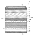
図18を参照して、発光素子は、導電型がn型のGaN基板である窒化物半導体基板10aと、n型GaN層41と、n型GaN層41上に形成されたAlGaN層42と、AlGaN層42上に形成された発光層43と、発光層43上に形成されたp型AlGaN層44と、p型AlGaN層44上に形成されたp型GaN層45とを備えている。n型のGaN基板である窒化物半導体基板10aは、たとえば1×10⁻²Ωcmという抵抗値であって、n型の導電性不純物の濃度が3×10¹⁸/cm3という特性を備える。n型GaN層41の厚みはたとえば1μmとすることができる。また、このn型GaN層に含有される導電性不純物としてはシリコン(Si)を用いることができる。また、n型AlGaN層42の厚みはたとえば150nmとすることができる。また、このn型AlGaN層42に含有される導電性不純物としてはたとえばシリコンを用いることができる。そして、このAlGaN層42の組成としては、たとえばAl0.1Ga0.9Nといった組成を用いることができる。
Referring to FIG. 18, the light emitting device includes a
また、発光層43としては、たとえば図19に示すような多重量子井戸構造を用いることができる。具体的には、発光層43は、GaN層43aとGaInN層43bとが交互に積層した多層構造となっていてもよい。このとき、たとえばGaN層43aの厚みを10nm、GaInN層43bの厚みを3nmとすることができる。また、GaInN層の組成としては、たとえばGa0.85In0.15Nといったものを用いることができる。
As the
そして、この発光層43上に位置するp型AlGaN層44の厚みはたとえば20nmとすることができる。また、このp型AlGaN層に含まれる導電性不純物としてはたとえばマグネシウム(Mg)を用いることができる。また、このp型AlGaN層44の組成としては、たとえばAl0.2Ga0.8Nといったものを用いることができる。
And the thickness of the p-
また、p型GaN層45の厚みはたとえば150nmとすることができる。さらに、このp型GaN層45に含まれる導電性不純物としてマグネシウムを用いることができる。
The thickness of the p-
図18および図19に示した半導体素子は、図4に示した基板の製造方法を用いて本発明による窒化物半導体基板10a〜10eのいずれかを準備し、その後当該窒化物半導体基板10a〜10eの主面11上に所定の膜をエピタキシャル成長させる工程を実施することにより形成することができる。
18 and FIG. 19, the
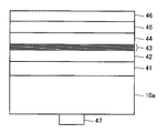
次に、図18および図19に示した半導体素子の表面および裏面に、図20に示すように電極を形成する。具体的には、図20を参照して、p型GaN層45上にp側電極46を形成する。このp側電極46としては、たとえばニッケル(Ni)と金(Au)との積層構造の電極を用いることができる。また、n型GaNからなる窒化物半導体基板10aの表面には、図20に示すようにn側電極47として、チタン(Ti)/アルミニウム(Al)/チタン(Ti)/金(Au)という積層構造の電極を用いることができる。n側電極47は、窒化物半導体基板10aの表面のほぼ中央部に配置する。一方、p側電極46は、p型GaN層45の表面を覆うように形成する。
Next, electrodes are formed on the front and back surfaces of the semiconductor element shown in FIGS. 18 and 19 as shown in FIG. Specifically, referring to FIG. 20, p-
次に、このようにして得られた発光素子を図21に示すようなステムに取付けることにより、発光装置を形成することができる。図21を参照して、図20に示した発光素子のp側電極46をステム52にハンダ53を介して接続固定する。一方、n側電極47は、ワイヤ54を介してリードピン51と電気的に接続される。このようにエピダウン(窒化物半導体基板10a上に形成されたエピタキシャル層側をステム52に向けて接続する構成)でステム52に実装された発光素子は、窒化物半導体基板10a(図20参照)であるn型GaN基板が透明であることから、当該基板側からも光を外部へ放出することができる。また、発光層43がステム52近くに配置されていることから、発光層から発生した熱がステム52へと伝達しやすく放熱性が良好である。なお、GaN基板も熱伝導率が高いため、当該基板側からも放熱が進む。
Next, a light emitting device can be formed by attaching the light emitting element thus obtained to a stem as shown in FIG. Referring to FIG. 21, the p-
発光素子の発光波長は、430nm〜550nmとすることができる。発光波長は発光層のIn組成により調整できる。本発明の窒化物半導体基板では、エピ成長時のInの取り込み効率を向上することができ、緑色領域の500nm〜550nmで良好な発光特性を得ることができる。 The light emission wavelength of the light emitting element can be set to 430 nm to 550 nm. The emission wavelength can be adjusted by the In composition of the light emitting layer. In the nitride semiconductor substrate of the present invention, the In incorporation efficiency at the time of epi growth can be improved, and good light emission characteristics can be obtained at 500 nm to 550 nm in the green region.
以下、上述した実施の形態と一部重複する部分もあるが、本発明の特徴的な構成を列挙する。 Hereinafter, although there is a part which overlaps with embodiment mentioned above, the characteristic structure of this invention is enumerated.
本発明に従った窒化物半導体基板10a〜10eは、(0001)面から[1−100]方向に71°以上79°以下傾斜、或いは(000−1)面から[−1100]方向に71°以上79°以下傾斜した主面11と、主面11の外周端部に位置する面取り加工部とを備える。面取り加工部の、主面11および当該主面11と反対側に位置する裏面21のうちのいずれか隣接する一方に対する傾斜角度(θ1またはθ2)は5°以上45°以下である。
The
本発明の窒化物半導体基板10a〜10eは、半導体装置を作製したときに歩留りを向上できる主面11を有している。さらに、窒化物半導体基板10a〜10eの外周端部からの割れや欠けの発生を抑制することができる。この結果、当該割れや欠けに起因する窒化物半導体基板10a〜10eの不良発生を抑制でき、当該窒化物半導体基板10a〜10eの歩留りを向上させることができる。
The
なお、主面11の傾斜角度を上記のように(0001)面から[1−100]方向に71°以上79°以下、或いは(000−1)面から[−1100]方向に71°以上79°以下としたのは、この範囲で特に半導体装置の歩留りを向上させることがでたからである。また、面取り加工部の傾斜角度θ1またはθ2の下限を5°としたのは、この角度より小さくなると当該基板の外周端部の角部が実質的に面取り加工部を形成しない場合とほとんど変わらなくなり、割れや欠けを抑制する効果が得られなくなるためである。また、当該傾斜角度の上限を45°としたのは、この角度より大きくすると、面取り加工部と主面との境界部の角部が135°より小さくなってしまい、当該角部での割れや欠けが問題となってくるためである。
The inclination angle of the
なお、面取り加工部の上記傾斜角度は、好ましくは15°以上35°以下、より好ましくは17°以上25°以下である。このような数値範囲としたのは、次工程(表面研削および裏面研削工程)にて発生するクラック、割れや欠けを防ぐ確率をより高くできる、という理由による。 The inclination angle of the chamfered portion is preferably 15 ° to 35 °, more preferably 17 ° to 25 °. The reason why such a numerical value range is set is that the probability of preventing cracks, cracks, and chips generated in the next process (surface grinding and back grinding process) can be further increased.
上記窒化物半導体基板10a〜10eにおいて、主面11は、(20−21)面または(−202−1)面から−0.5°以上0.5°以下傾斜した面であってもよい。ここで、上述した面を主面11とする窒化物半導体基板10a〜10eは、半導体装置を作製したときに特に特性を向上することができる。
In the
上記窒化物半導体基板10a〜10eにおいて、面取り加工部の表面層には、平均厚さが0.5μm以上10μm以下である加工変質層25が形成されていてもよい。
In the
この場合、窒化物半導体基板10a〜10eの外周端部に加工変質層25が形成されることにより、当該外周端部において残留応力が存在する領域を配置することができる。この結果、当該加工変質層25の厚さを適宜調整することにより、窒化物半導体基板10a〜10eの形状が反ったりするという形状不良を抑制する効果を得ることができる。
In this case, by forming the work-affected
なお、加工変質層25の平均厚さは、TEM(透過型電子顕微鏡)で測定することができる。そして、当該平均厚さの下限を0.5μmとしたのは、面取り加工部を研磨や研削により形成する場合に、0.5μmより厚さの薄い加工変質層では反り抑制の効果が小さく、デバイスの歩留が低下するからである。また、当該平均厚さの上限を10μmとしたのは、10μmより厚い加工変質層を形成するとクラックおよび割れが発生する確率が増加し、さらにデバイスの歩留が低下するからである。
The average thickness of the work-affected
なお、加工変質層25の平均厚さは、好ましくは1μm以上5μm以下である。このような数値範囲としたのは、1μm以下の加工は砥石が高番手になり、加工時間が長くなるため製造コストが大きくなり、また、5μm以上の加工は砥石が低番手(粗く)になるためパーティクルの発生などの問題からデバイスの歩留が低下する、という理由による。
The average thickness of the work-affected
上記窒化物半導体基板10a〜10eにおいて、面取り加工部の面取り量(図2における幅L1、L2)は0.02mm以上0.5mm以下であってもよい。この場合、窒化物半導体基板10a〜10eの外周端部からの割れや欠けの発生を抑制する効果を確実に得ることができる。
In the
なお、面取り量の下限を0.02mmとしたのは、この値より小さくなると当該基板の外周端部の角部が実質的に面取り加工部を形成しない場合とほとんど変わらなくなり、割れや欠けを抑制する効果が得られなくなるためである。また、面取り量の上限を0.5mmとしたのは、これより大きな面取り量とすると、基板の主面において面取り加工部の面積が大きくなりすぎ、当該基板から得られる半導体装置の数が少なくなって結果的に半導体装置の製造コストが増大するためである。 Note that the lower limit of the chamfering amount is set to 0.02 mm. If the chamfering amount is smaller than this value, the corners of the outer peripheral edge of the substrate are substantially the same as when the chamfered portion is not formed, and cracking and chipping are suppressed. This is because the effect of this cannot be obtained. Further, the upper limit of the chamfering amount is set to 0.5 mm. If the chamfering amount is larger than this, the area of the chamfered portion becomes too large on the main surface of the substrate, and the number of semiconductor devices obtained from the substrate is reduced. As a result, the manufacturing cost of the semiconductor device increases.
なお、上記面取り量は、好ましくは0.05mm以上0.3mm以下、より好ましくは0.05mm以上0.2mm以下である。このような数値範囲としたのは、面取り量が大きいと(研削量が多いため)加工中基板に負荷が多くかかりクラックなどの不良になる確率が大きくなる、という理由による。 The chamfering amount is preferably 0.05 mm or more and 0.3 mm or less, more preferably 0.05 mm or more and 0.2 mm or less. The reason why such a numerical range is set is that if the chamfering amount is large (because the grinding amount is large), the load is increased on the substrate during processing, and the probability of defects such as cracks increases.
上記窒化物半導体基板10a〜10eにおいて、面取り加工部の表面の算術平均粗さはRaで0.07μm以上3μm以下であってもよい。
In the
この場合、面取り加工部の表面粗さが粗すぎて問題が発生する(たとえばパーティクルが発生する)ことを抑制できる。なお、上記表面粗さの下限をRaで0.07μmとしたのは、現実的なコストでこの値より表面粗さを小さくすることが困難なためである。また、上記表面粗さの上限をRaで3μmとしたのは、この値より大きいとパーティクルの発生などの問題が起きる可能性が高くなるからである。 In this case, it is possible to suppress the occurrence of a problem (for example, generation of particles) due to the surface roughness of the chamfered portion being too rough. The lower limit of the surface roughness is set to 0.07 μm in Ra because it is difficult to reduce the surface roughness below this value at a practical cost. Moreover, the upper limit of the surface roughness is set to 3 μm in Ra because if it is larger than this value, there is a high possibility that problems such as generation of particles will occur.
また、上記表面粗さは、好ましくはRaで0.07μm以上1μm以下、より好ましくはRaで0.07μm以上0.5μm以下である。このような数値範囲としたのは、Raが小さいほどより微細なパーティクル(不純物)の発生を抑制し、デバイス素子歩留がより高くなるため、という理由による。 The surface roughness is preferably 0.07 to 1 μm in Ra, more preferably 0.07 to 0.5 μm in Ra. The reason why such a numerical value range is set is that, as Ra is smaller, the generation of finer particles (impurities) is suppressed and the device element yield is further increased.
上記窒化物半導体基板10a〜10eにおいて、主面11は鏡面加工されていてもよい。主面11の表面粗さは二乗平均粗さ(RMS)で0.2nm以上4nm以下であってもよい。
In the
この場合、主面11上にエピタキシャル膜を形成するときに、当該エピタキシャル膜の成膜不良の発生を抑制できる。
In this case, when an epitaxial film is formed on the
なお、主面11の表面粗さの下限を上記のような値としたのは、上記の値より小さい表面粗さとすることは工業的に現実的なコストでは困難だからである。また、上記表面粗さの上限を上記の値としたのは、上記の値より大きいとエピタキシャル膜の成膜不良の発生確率が増大するためである。
The reason why the lower limit of the surface roughness of the
また、上記主面11の表面粗さは、好ましくはRMSで1nm以上3nm以下である。このような数値範囲としたのは、上述した理由と同様にコストと品質の点で当該数値範囲が好ましいから、という理由による。
The surface roughness of the
上記窒化物半導体基板10a〜10eには、所定の面を示す表示部(オリフラ12、13、ノッチ15、16、印17)が形成されていてもよい。
The
この場合、窒化物半導体基板10a〜10eのハンドリング時や当該窒化物半導体基板10a〜10eを用いて半導体装置(図18〜21参照)を製造する場合に、窒化物半導体基板10a〜10eの面方位を確実に把握することができる。
In this case, when the
上記窒化物半導体基板10a〜10eにおいて、表示部が示す所定の面は(−1017)面、(10−1−7)面、またはこれらの面から−0.5°以上0.5°以下傾斜した面、または(11−20)面、またはこの面から−0.5°以上0.5°以下傾斜した面であってもよい。
In the
ここで、本発明の窒化物半導体基板10a〜10eは、半導体装置を作製したときに歩留まりを向上できる主面11を有している。そして、この主面11を有する窒化物半導体基板10a〜10eを半導体装置に用いるために面方位を特定することを鋭意研究した結果、(−1017)面および(10−1−7)面近傍が劈開しやすい性質を有していることを発明者は見出した。そして、発明者は、この主面を有する窒化物半導体基板において、表示部により(−1017)面、(10−1−7)面、またはこれらの面から−0.5°以上0.5°以下傾斜した面を特定することを初めて明らかにした。この表示部により、この主面11を有する窒化物半導体基板10a〜10eを用いて半導体装置を作製するときに、劈開しやすい面を特定することができる。これにより、劈開しやすい面を用いて、結晶方位の位置合わせまたは判別をすることができる。このため、本発明の窒化物半導体基板10a〜10eを用いることにより、特性を向上した半導体装置を作製することができる。したがって、本発明の窒化物半導体基板10a〜10eを半導体装置に用いることができる。
Here, the
この発明に従った窒化物半導体基板の製造方法は、(0001)面から[1−100]方向に71°以上79°以下傾斜、或いは(000−1)面から[−1100]方向に71°以上79°以下傾斜した主面を有する窒化物半導体基板を準備する工程(S10)と、窒化物半導体基板の主面の外周端部に面取り加工を施す工程(S20)とを備える。面取り加工を施す工程(S20)では、主面11および主面と反対側に位置する裏面21のうちのいずれか隣接する一方に対する傾斜角度(θ1またはθ2)が5°以上45°以下となる面取り加工部を形成する。このようにすれば、本発明に従った窒化物半導体基板10a〜10eを製造することができる。
The method for producing a nitride semiconductor substrate according to the present invention is inclined from 71 ° to 79 ° in the [1-100] direction from the (0001) plane, or 71 ° from the (000-1) plane in the [−1100] direction. A step (S10) of preparing a nitride semiconductor substrate having a main surface inclined by 79 ° or less and a step (S20) of chamfering the outer peripheral end of the main surface of the nitride semiconductor substrate are provided. In the chamfering step (S20), the chamfering in which the inclination angle (θ1 or θ2) with respect to any one of the
この発明に従った半導体装置は、図18〜21に示すように、上記窒化物半導体基板10a〜10eを用いた半導体装置である。この場合、窒化物半導体基板10a〜10eの割れや欠けが効果的に抑制されることから、製造歩留りの高い半導体装置を実現できる。
A semiconductor device according to the present invention is a semiconductor device using the
この発明に従った半導体装置の製造方法は、図4に示した上記窒化物半導体基板の製造方法を用いて窒化物半導体基板10a〜10eを準備する工程と、窒化物半導体基板10a〜10eの主面11上にエピタキシャル層を形成する工程とを備える。この場合、窒化物半導体基板10a〜10eの割れや欠けが効果的に抑制されることから、半導体装置の高い製造歩留りを実現できる。
A method for manufacturing a semiconductor device according to the present invention includes a step of preparing
本実施例では、(0001)GaNインゴットから[1−100]方向に68度から82度の範囲の角度θで切り出したGaN基板の有用性を調べた(試験1)。具体的には、上記角度θを変えた基板を用いて半導体レーザの素子を形成し、当該素子の発振歩留まりを測定した。また、面取り加工部の、主面11および当該主面11と反対側に位置する裏面21のうちのいずれか隣接する一方に対する傾斜角度(θ1またはθ2)の優位性についても調べた(試験2)。
In this example, the usefulness of the GaN substrate cut out from the (0001) GaN ingot in the [1-100] direction at an angle θ ranging from 68 degrees to 82 degrees was examined (Test 1). Specifically, a semiconductor laser element was formed using a substrate with the angle θ changed, and the oscillation yield of the element was measured. Further, the superiority of the inclination angle (θ1 or θ2) of the chamfered portion with respect to one of the
(試験1)
試料の準備:
まず、HVPE法で厚く成長した(0001)GaNインゴットから[1−100]方向に68度から82度の範囲の角度θでウェハスライス装置を用いて切り出し、[0001]方向から[1−100]方向への傾斜角度θが、68度から82度の範囲の所望のオフ角を有するGaN基板(後述する表1における試料ID:I−1〜I−9)を作製した。たとえば、75°の角度θで切り出したとき、(20−21)面を主面として有するGaN基板が得られ、六方晶系の結晶格子において主面11によって示される。
(Test 1)
Sample preparation:
First, a (0001) GaN ingot grown thick by the HVPE method was cut out using a wafer slicing device at an angle θ in the range of 68 to 82 degrees in the [1-100] direction, and [1-100] from the [0001] direction. A GaN substrate (sample IDs: I-1 to I-9 in Table 1 to be described later) having a desired off angle with a tilt angle θ in the direction in the range of 68 degrees to 82 degrees was manufactured. For example, when cut at an angle θ of 75 °, a GaN substrate having a (20-21) plane as a main surface is obtained, and is indicated by the
なお、当該GaN基板においては、外周端部に面取り加工部(チャンファー加工部)を形成した。なお、チャンファー加工にレジンボンド砥石を使うと、GaN基板の外周部から割れたりクラックが入ったりする。そこで割れやクラックを防ぐために本実施例ではゴム砥石を使って加工を行なった。具体的には、1000番手ダイヤモンド砥粒40 wt%とFe2O3砥粒60wt% の混合物をCR(クロロプレンゴム)で基盤に固定した砥石を用いて外周研削した。このときの表面の算術平均粗さ(Ra)は0.1μmであった。当該ゴム砥石の空孔率は0%であり、又、基板の同じ厚みのものを使用し、面取り加工部の形状(チャンファー形状)は表裏で対称になる図11に示した形状を基準とした。面取り部の角度(面取り角度)は20°に、面取り量は0.2mmに統一した。なお、基板厚み、表裏の面取り角度及び面取り量が決まれば、残りの長さが決まるので、その間は滑らかな曲面でつなぐことができる。
In the GaN substrate, a chamfered portion (chamfered portion) was formed at the outer peripheral end. In addition, when a resin bond grindstone is used for chamfering, the GaN substrate is cracked or cracked from the outer periphery. Therefore, in this embodiment, processing was performed using a rubber grindstone in order to prevent cracks and cracks. Specifically, peripheral grinding was performed using a grindstone in which a mixture of 1000 count diamond
また、このGaN基板について、(−1017)面であるオリフラを形成した。
次に、当該GaN基板を用いて半導体レーザを有機金属気相成長法により形成した。形成した半導体レーザ100は、図22および図23に示した構成を備える。また、有機金属気相成長法における原料にはトリメチルガリウム(TMGa)、トリメチルアルミニウム(TMAl)、トリメチルインジウム(TMIn)、アンモニア(NH3)、シラン(SiH4)を用いた。
In addition, an orientation flat having a (−1017) plane was formed on the GaN substrate.
Next, a semiconductor laser was formed by metal organic vapor phase epitaxy using the GaN substrate. The formed
具体的には、GaN基板を窒化物半導体基板10aとして反応炉内のサセプタ上に配置した後に、以下の成長手順でエピタキシャル層を成長した。まず、図22を参照して、窒化物半導体基板10a(GaN基板)の主表面上にn型バッファ層102として、厚さ1000nmのn型GaNを成長した。次に、n型クラッド層103として、厚さ1200nmのn型InAlGaNクラッド層を成長した。引き続き、n型ガイド層104として、厚さ200nmのn型GaNガイド層、およびアンドープガイド層105として、厚さ65nmのアンドープInGaNガイド層を成長した。その後、活性層106として、厚さ15nmのGaN/厚さ3nmのInGaNから構成される3周期MQWを成長した。続いて、アンドープガイド層107として、厚さ65nmのアンドープInGaNガイド層、p型ブロック層108として、厚さ20nmのp型AlGaNブロック層、およびp型ガイド層109として、厚さ200nmのp型GaNガイド層を成長した。次に、p型クラッド層110として、厚さ400nmのp型InAlGaNクラッド層を成長した。最後に、p型コンタクト層111として、厚さ50nmのp型GaNコンタクト層を成長した。
Specifically, after the GaN substrate was placed on the susceptor in the reactor as the
次に、SiO2の絶縁膜112をp型コンタクト層111上に成膜した後に、当該絶縁膜112にフォトリソグラフィ法を用いて幅10μmのストライプ窓をウエットエッチングにより形成した。ここで、オリフラ12により上記エピタキシャル層において[−1014]方向を特定できるので、図23に示すようにレーザストライプの方向は[−1014]方向から−0.5°以上0.5°以下傾斜した方向とした。
Next, after an
そして、絶縁膜112の開口部(ストライプ窓)が上記方向に形成されているので、図23に示すように半導体レーザ100の導波路100cの方位は、[−1014]方向、またはこれらの方向から[1−100]方向に−4°以上4°以下傾斜し、かつ[1−100]方向に直交する方向に−0.5°以上0.5°以下である。つまり、導波路100cは、端面100a、100b((−1017)面、(10−1−7)面、またはこれらの面から[1−100]方向に−4°以上4°以下傾斜し、かつ[1−100]方向に直交する方向に−0.5°以上0.5°以下傾斜した面)に概ね垂直な方向に形成される。
Since the opening (stripe window) of the insulating
次に、ストライプ窓を形成した後に、Ni/Auからなるp型電極113とTi/Alからなるパッド電極(図示せず)を蒸着した。次いで、GaN基板(窒化物半導体基板10a)の裏面を、ダイヤモンドスラリーを用いて劈開がより容易になる100μm以下の基板厚みになるまで研磨し、裏面がミラー状態の基板生産物を作製した。GaN基板の裏面(研磨面)にはTi/Al/Ti/Auからなるn型電極114を蒸着により形成した。
Next, after forming a stripe window, a p-
このレーザストライプに対する共振器ミラーの作製には、波長355nmのYAGレーザを用いるレーザスクライバを用いた。レーザスクライバを用いてブレイクした場合には、ダイヤモンドスクライブを用いた場合と比較して、発振チップ歩留まりを向上させることが可能である。スクライブ溝の形成条件として、レーザ光出力を100mW、走査速度を5mm/sとした。形成されたスクライブ溝は、たとえば、長さ30μm、幅10μm、深さ40μmの溝であった。800μmピッチでGaN基板の絶縁膜開口箇所を通してエピタキシャル層の表面に直接レーザ光を照射することによって、スクライブ溝を形成した。共振器長は600μmとした。 A laser scriber using a YAG laser having a wavelength of 355 nm was used for manufacturing the resonator mirror for the laser stripe. When a break is made using a laser scriber, it is possible to improve the oscillation chip yield compared to the case where diamond scribe is used. As conditions for forming the scribe grooves, the laser beam output was 100 mW and the scanning speed was 5 mm / s. The formed scribe groove was, for example, a groove having a length of 30 μm, a width of 10 μm, and a depth of 40 μm. A scribe groove was formed by directly irradiating the surface of the epitaxial layer with a laser beam through the insulating film opening of the GaN substrate at a pitch of 800 μm. The resonator length was 600 μm.
ブレードを用いて、共振ミラーを割断により作製した。GaN基板裏側にブレードを押圧して基板生産物をブレイクすることによって、レーザバーを作製した。より具体的には、図24に示すように、主面11と共にレーザ共振器のための端面100a、100bは、(−1017)面、(10−1−7)面であり、従来のc面、m面またはa面等のこれまでの劈開面とは異なる。
Using a blade, a resonant mirror was prepared by cleaving. Laser bars were fabricated by pressing the blade against the backside of the GaN substrate to break the substrate product. More specifically, as shown in FIG. 24, the end faces 100a and 100b for the laser resonator together with the
なお、ブレイクによって形成された割断面を走査型電子顕微鏡で観察した結果、顕著な凹凸は観察されなかった。このことから、割断面の平坦性(凹凸の大きさ)は、20nm以下と推定される。さらに、割断面の試料表面に対する垂直性は、±5°の範囲内であった。 In addition, as a result of observing the fractured surface formed by the break with a scanning electron microscope, remarkable unevenness was not observed. From this, the flatness (size of irregularities) of the fractured surface is estimated to be 20 nm or less. Furthermore, the perpendicularity of the fractured surface to the sample surface was within a range of ± 5 °.
次に、レーザバーの端面に真空蒸着法によって誘電体多層膜をコーティングした。誘電体多層膜は、SiO2(酸化ケイ素)とTiO2(二酸化チタン)を交互に積層して構成した。膜厚はそれぞれ、50nm以上100nm以下の範囲で調整して、反射率の中心波長が500nm以上530nm以下の範囲になるように設計した。片側の反射面を10周期とし、反射率の設計値を約95%に設計し、もう一方側の反射面を6周期とし、反射率の設計値を約80%とした。 Next, a dielectric multilayer film was coated on the end face of the laser bar by vacuum deposition. The dielectric multilayer film was configured by alternately laminating SiO 2 (silicon oxide) and TiO 2 (titanium dioxide). Each film thickness was adjusted in the range of 50 nm or more and 100 nm or less, and designed so that the central wavelength of the reflectance was in the range of 500 nm or more and 530 nm or less. The reflective surface on one side was set to 10 periods, the design value of reflectivity was designed to about 95%, the reflective surface on the other side was set to 6 periods, and the design value of reflectivity was about 80%.
試験および結果:
このように作製した半導体レーザについて、GaN基板主面の、(0001)面からの[1−100]方向への傾斜角度θ(主面の角度)と発振歩留まりとの関係を調べた。なお、本実施例では、発振歩留まりについては、(発振チップ数)/(測定チップ数)と定義した。その結果を表1に示す。
Tests and results:
For the semiconductor laser fabricated in this way, the relationship between the inclination angle θ (main surface angle) of the GaN substrate main surface in the [1-100] direction from the (0001) plane and the oscillation yield was examined. In this example, the oscillation yield was defined as (number of oscillation chips) / (number of measurement chips). The results are shown in Table 1.

表1より、GaN基板の[1−100]方向への[0001]方向の傾斜角度θ(表1に記載された主面の角度)が71°以上79°以下の範囲で発振歩留まり50%以上と、良好な結果が得られた。 From Table 1, the oscillation yield of 50% or more in the range of the inclination angle θ of the [0001] direction to the [1-100] direction of the GaN substrate (angle of the main surface described in Table 1) is 71 ° or more and 79 ° or less. Good results were obtained.
(試験2)
試験2では、上記傾斜角度θ(主面の角度)が75°の基板を中心に実験を行った。具体的には、表裏の面取り角度を変えて素子歩留まり及び基板歩留まりを調べた。基板歩留は、基板にクラック、割れおよびカケが生じない割合であり、(目視による確認の結果クラックや割れ、カケが発生しなかった基板の数)/(測定した基板の数)と定義した。
(Test 2)
In Test 2, the experiment was conducted centering on a substrate having the inclination angle θ (main surface angle) of 75 °. Specifically, the element yield and the substrate yield were examined by changing the chamfer angles on the front and back sides. Substrate yield is the rate at which cracks, cracks and chips do not occur on the substrate, and is defined as (number of substrates where cracks, cracks and chips did not occur as a result of visual confirmation) / (number of substrates measured). .
試料の準備:
上述した試験1において準備した試料と基本的に同様の方法によりGaN基板の試料(後述する表2における試料ID:II−1〜II−11)および半導体レーザの試料を作製した。ただし、後述する表2に示すように主面の角度(傾斜角度θ)は75°、71°または79°とした。さらに、各試料については、面取り加工部の面取り角度を表2に示すように0°〜60°の範囲で変更している。このとき1000番手の砥石を使用し面取りを行った。又、基板は同じ厚みのものを使用し、面取り加工部の形状(チャンファー形状)は表裏で対称になる図11に示した形状を基準とした。面取り量は0.2mmに統一した。
Sample preparation:
A sample of a GaN substrate (sample IDs: II-1 to II-11 in Table 2 described later) and a sample of a semiconductor laser were fabricated by a method basically similar to that of the sample prepared in the
試験および結果:
このように作製したGaN基板の試料について、クラックや割れ、カケといった不良の発生状況を目視で確認することにより、基板歩留まりを算出した。さらに、GaN基板の各試料を用いて作製した半導体レーザについて、発振歩留まり(素子歩留まり)を試験1と同様に測定した。その結果を表2に示す。
Tests and results:
The yield of the substrate was calculated by visually checking the occurrence of defects such as cracks, cracks, and chipping for the GaN substrate sample thus produced. Furthermore, the oscillation yield (element yield) was measured in the same manner as in
表2に示すように、面取り角度が5°以上45°以下で基板歩留まり50%以上の良好な結果が得られた。又、面取り加工部について表面側と裏面側とで面取り量や面取り角度を変更した場合でも同様の結果が得られた。 As shown in Table 2, good results were obtained with a substrate yield of 50% or more when the chamfer angle was 5 ° or more and 45 ° or less. The same result was obtained even when the chamfering amount and the chamfering angle were changed between the front surface side and the back surface side of the chamfered portion.
さらに、主面の角度(傾斜角度θ)が71°から79°の範囲でも同様の結果が得られた。なお、フラックス法で成長した結晶についても、上記と同等の結果が得られた。また、下地基板に複数のGaN基板を用い、HVPE法での成長で下地基板から接合した単一のGaN結晶を成長させた場合においても、上記と同等の結果が得られた。 Further, similar results were obtained even when the angle of the main surface (inclination angle θ) was in the range of 71 ° to 79 °. The same results as above were obtained for crystals grown by the flux method. In addition, when a plurality of GaN substrates were used as the base substrate and a single GaN crystal joined from the base substrate was grown by the HVPE method, the same result as above was obtained.
本実施例では、面取り加工部の加工条件(チャンファー加工条件)を変えて、面取り加工部における加工変質層の厚みを変えた基板を用い、当該加工変質層の厚みの影響を調べた。具体的には、面取り加工部における加工変質層の厚みを変えたGaN基板の試料を準備した。そして、当該GaN基板を用いて実施例1と同じ構造の半導体レーザを作製し、素子歩留まりを調べた。 In this example, the influence of the thickness of the work-affected layer was examined using a substrate in which the thickness of the work-affected layer in the chamfered portion was changed by changing the processing conditions (chamber processing conditions) of the chamfered portion. Specifically, a sample of a GaN substrate in which the thickness of the work-affected layer in the chamfered portion was changed was prepared. Then, a semiconductor laser having the same structure as that of Example 1 was manufactured using the GaN substrate, and the element yield was examined.
試料の準備:
基本的に、実施例1におけるGaN基板の製造方法と同様の製造方法によりGaN基板の試料(後述する表3における試料ID:III−1〜III−9)を作製した。なお、加工変質層の厚さは、面取り加工に用いるゴム砥石の番手などを調整することで変更した。また、GaN基板主面の、(0001)面からの[1−100]方向への傾斜角度θ(主面の角度)は75°または73°とした。
Sample preparation:
Basically, samples of the GaN substrate (sample IDs: III-1 to III-9 in Table 3 to be described later) were manufactured by the same manufacturing method as that of the GaN substrate in Example 1. The thickness of the work-affected layer was changed by adjusting the count of a rubber grindstone used for chamfering. In addition, the inclination angle θ (angle of the main surface) of the GaN substrate main surface in the [1-100] direction from the (0001) plane was set to 75 ° or 73 °.
そして、得られたGaN基板を用いて実施例1と同様に半導体レーザを作製した。又、基板は同じ厚みのものを使用し、面取り加工部の形状(チャンファー形状)は表裏で対称になる図11に示した形状を基準とした。面取り角度は20°に面取り量は0.2mmに統一した。 Then, a semiconductor laser was produced in the same manner as in Example 1 using the obtained GaN substrate. Further, substrates having the same thickness were used, and the shape of the chamfered portion (chamber shape) was based on the shape shown in FIG. The chamfer angle was unified to 20 ° and the chamfer amount to 0.2 mm.
試験および結果:
製造した半導体レーザについて、発振実験を行なうことで、面取り加工部の加工変質層厚さ(平均加工変質層厚さ)と発振歩留まり(素子歩留まり)との関係を調べた。その結果を表3に示す。
Tests and results:
Oscillation experiments were performed on the manufactured semiconductor lasers to investigate the relationship between the work-affected layer thickness (average work-affected layer thickness) of the chamfered portion and the oscillation yield (element yield). The results are shown in Table 3.
表3より、面取り部分の平均加工変質層厚さが0.5μm以上10μm以下で素子歩留まり50%以上の良好な結果が得られた。又、面取り加工部について表面側と裏面側とで面取り量や面取り角度を変更した場合でも同様の結果が得られた。なお、フラックス法で成長した結晶についても、上記と同等の結果が得られた。また、下地基板に複数のGaN基板を用い、HVPE法での成長で下地基板から接合した単一のGaN結晶を成長させた場合においても、上記と同等の結果が得られた。 From Table 3, good results were obtained in which the average work-affected layer thickness in the chamfered portion was 0.5 μm or more and 10 μm or less and the device yield was 50% or more. The same result was obtained even when the chamfering amount and the chamfering angle were changed between the front surface side and the back surface side of the chamfered portion. The same results as above were obtained for crystals grown by the flux method. In addition, when a plurality of GaN substrates were used as the base substrate and a single GaN crystal joined from the base substrate was grown by the HVPE method, the same result as above was obtained.
本実施例では、面取り加工部の加工条件(チャンファー加工条件)を変えて、面取り加工部における面取り量を変えた基板を用い、当該面取り量の影響を調べた。具体的には、面取り加工部における面取り量を変えたGaN基板の試料を準備し、基板歩留まりを調べた。 In this example, the influence of the chamfering amount was examined using a substrate in which the chamfering part was changed by changing the processing conditions (chamber processing conditions) of the chamfering part. Specifically, GaN substrate samples with different chamfered amounts in the chamfered portion were prepared, and the substrate yield was examined.
試料の準備:
基本的に、実施例1におけるGaN基板の製造方法と同様の製造方法によりGaN基板の試料(後述する表4における試料ID:IV−1〜IV−9)を作製した。なお、GaN基板主面の、(0001)面からの[1−100]方向への傾斜角度θ(主面の角度)は75°または74°とした。このとき1000番手の砥石を使用し面取りを行った。又、基板は同じ厚みのものを使用し、面取り加工部の形状(チャンファー形状)は表裏で対称になる図11に示した形状を基準とした。面取り角度は20°に統一した。
Sample preparation:
Basically, GaN substrate samples (sample IDs: IV-1 to IV-9 in Table 4 to be described later) were manufactured by the same manufacturing method as that of the GaN substrate in Example 1. In addition, the inclination angle θ (angle of the main surface) of the GaN substrate main surface in the [1-100] direction from the (0001) plane was set to 75 ° or 74 °. At this time, chamfering was performed using a 1000th grindstone. Further, substrates having the same thickness were used, and the shape of the chamfered portion (chamber shape) was based on the shape shown in FIG. The chamfer angle was unified to 20 °.
試験および結果:
このように作製したGaN基板の試料について、クラックや割れ、カケといった不良の発生状況を目視で確認することにより、基板歩留まりを算出した。その結果を表4に示す。
Tests and results:
The yield of the substrate was calculated by visually checking the occurrence of defects such as cracks, cracks, and chipping for the GaN substrate sample thus produced. The results are shown in Table 4.
表4より、面取り量が0.02mm以上0.5mm以下で基板歩留まり50%以上の良好な結果が得られた。又、面取り加工部について表面側と裏面側とで面取り量や面取り角度を変更した場合でも同様の結果が得られた。なお、フラックス法で成長した結晶についても、上記と同等の結果が得られた。また、下地基板に複数のGaN基板を用い、HVPE法での成長で下地基板から接合した単一のGaN結晶を成長させた場合においても、上記と同等の結果が得られた。 From Table 4, good results were obtained with a substrate yield of 50% or more when the chamfering amount was 0.02 mm or more and 0.5 mm or less. The same result was obtained even when the chamfering amount and the chamfering angle were changed between the front surface side and the back surface side of the chamfered portion. The same results as above were obtained for crystals grown by the flux method. In addition, when a plurality of GaN substrates were used as the base substrate and a single GaN crystal joined from the base substrate was grown by the HVPE method, the same result as above was obtained.
本実施例では、面取り加工部の加工条件(チャンファー加工条件)を変えて、面取り加工部における表面粗さを変えた基板を用い、当該表面粗さの影響を調べた。具体的には、面取り加工部における表面粗さを変えたGaN基板の試料を準備した。そして、当該GaN基板を用いて実施例1と同じ構造の半導体レーザを作製し、素子歩留まりを調べた。 In this example, the influence of the surface roughness was examined using a substrate in which the surface roughness in the chamfered portion was changed by changing the processing conditions (chamber processing conditions) of the chamfered portion. Specifically, a sample of a GaN substrate with different surface roughness in the chamfered portion was prepared. Then, a semiconductor laser having the same structure as that of Example 1 was manufactured using the GaN substrate, and the element yield was examined.
試料の準備:
基本的に、実施例1におけるGaN基板の製造方法と同様の製造方法によりGaN基板の試料(後述する表5における試料ID:V−1〜V−9)を作製した。なお、面取り加工部の表面の算術平均粗さ(Ra)は、面取り加工に用いるゴム砥石の番手などを調整することで変更した。また、GaN基板主面の、(0001)面からの[1−100]方向への傾斜角度θ(主面の角度)は75°または76°とした。又、基板は同じ厚みのものを使用し、面取り加工部の形状(チャンファー形状)は表裏で対称になる図11に示した形状を基準とした。面取り角度は20°に面取り量は0.2mmに統一した。
Sample preparation:
Basically, samples of the GaN substrate (sample IDs: V-1 to V-9 in Table 5 described later) were manufactured by the same manufacturing method as that of the GaN substrate in Example 1. The arithmetic average roughness (Ra) of the surface of the chamfered portion was changed by adjusting the count of a rubber grindstone used for chamfering. In addition, the inclination angle θ (angle of the main surface) of the GaN substrate main surface in the [1-100] direction from the (0001) plane was set to 75 ° or 76 °. Further, substrates having the same thickness were used, and the shape of the chamfered portion (chamber shape) was based on the shape shown in FIG. The chamfer angle was unified to 20 ° and the chamfer amount to 0.2 mm.
そして、得られたGaN基板を用いて実施例1と同様に半導体レーザを作製した。
試験および結果:
製造した半導体レーザについて、発振実験を行なうことで、面取り加工部の表面粗さ(面取り部粗さ)と発振歩留まり(素子歩留まり)との関係を調べた。その結果を表5に示す。
Then, a semiconductor laser was produced in the same manner as in Example 1 using the obtained GaN substrate.
Tests and results:
By conducting an oscillation experiment on the manufactured semiconductor laser, the relationship between the surface roughness of the chamfered portion (chamfered portion roughness) and the oscillation yield (element yield) was investigated. The results are shown in Table 5.
表5より、面取り加工部の表面粗さが0.07μm以上3μm以下で素子歩留まり50%以上の良好な結果が得られた。又、面取り加工部について表面側と裏面側とで面取り量や面取り角度を変更した場合でも同様の結果が得られた。なお、フラックス法で成長した結晶についても、上記と同等の結果が得られた。また、下地基板に複数のGaN基板を用い、HVPE法での成長で下地基板から接合した単一のGaN結晶を成長させた場合においても、上記と同等の結果が得られた。 From Table 5, good results were obtained with a device yield of 50% or more when the surface roughness of the chamfered portion was 0.07 μm or more and 3 μm or less. The same result was obtained even when the chamfering amount and the chamfering angle were changed between the front surface side and the back surface side of the chamfered portion. The same results as above were obtained for crystals grown by the flux method. In addition, when a plurality of GaN substrates were used as the base substrate and a single GaN crystal joined from the base substrate was grown by the HVPE method, the same result as above was obtained.
以上のように本発明の実施の形態について説明を行なったが、各実施の形態の特徴を適宜組み合わせることも当初から予定している。また、今回開示された実施の形態および実施例はすべての点で例示であって制限的なものではないと考えられるべきである。本発明の範囲は上記した実施の形態ではなくて特許請求の範囲によって示され、特許請求の範囲と均等の意味および範囲内でのすべての変更が含まれることが意図される。 Although the embodiments of the present invention have been described as described above, it is also planned from the beginning to combine the features of each embodiment as appropriate. The embodiments and examples disclosed this time should be considered as illustrative in all points and not restrictive. The scope of the present invention is shown not by the above-described embodiment but by the scope of claims, and is intended to include all modifications within the meaning and scope equivalent to the scope of claims.
この発明は、半極性面である主面を有する窒化物半導体基板および当該窒化物半導体基板を用いた半導体装置に特に有利に適用される。 The present invention is particularly advantageously applied to a nitride semiconductor substrate having a main surface that is a semipolar surface and a semiconductor device using the nitride semiconductor substrate.
10a〜10e 窒化物半導体基板、11 主面、12,13 オリエンテーションフラット(オリフラ)、15,16 ノッチ、17 印、21 裏面、22 表側面取り部、23 裏側面取り部、24 端面、25 加工変質層、30 ゴム砥石、31,32 表面、41 n型GaN層、42 n側AlGaN層、43 発光層、43a GaN層、43b GaInN層、44 p型AlGaN層、45 p型GaN層、46 p側電極、47 n側電極、51 リードピン、52 ステム、53 ハンダ、54 ワイヤ、100 半導体レーザ、100a,100b 端面、100c 導波路、102 n型バッファ層、103 n型クラッド層、104 n型ガイド層、105,107 アンドープガイド層、106 活性層、108 p型ブロック層、109 p型ガイド層、110 p型クラッド層、111 p型コンタクト層、112 絶縁膜、113 p型電極、114 n型電極。 10a to 10e Nitride semiconductor substrate, 11 main surface, 12, 13 orientation flat (orientation flat), 15, 16 notch, 17 mark, 21 back surface, 22 front side chamfered portion, 23 back side chamfered portion, 24 end surface, 25 work-affected layer, 30 rubber grindstone, 31 and 32 surfaces, 41 n-type GaN layer, 42 n-side AlGaN layer, 43 light-emitting layer, 43a GaN layer, 43b GaInN layer, 44 p-type AlGaN layer, 45 p-type GaN layer, 46 p-side electrode, 47 n-side electrode, 51 lead pin, 52 stem, 53 solder, 54 wire, 100 semiconductor laser, 100a, 100b end face, 100c waveguide, 102 n-type buffer layer, 103 n-type cladding layer, 104 n-type guide layer, 105, 107 undoped guide layer, 106 active layer, 108 p-type block layer 109 p-type guide layer, 110 p-type clad layer, 111 p-type contact layer, 112 an insulating layer, 113 p-type electrode, 114 n-type electrode.
Claims (9)
(0001)面から[1−100]方向に71°以上79°以下傾斜、或いは(000−1)面から[−1100]方向に71°以上79°以下傾斜した主面と、
前記主面の外周端部に位置する面取り加工部とを備え、
前記面取り加工部の、前記主面および前記主面と反対側に位置する裏面のうちのいずれか隣接する一方に対する傾斜角度は5°以上45°以下である、窒化物半導体基板。 A nitride semiconductor substrate,
A main surface inclined from 71 ° to 79 ° in the [1-100] direction from the (0001) plane, or from 71 ° to 79 ° in the [-1100] direction from the (000-1) plane;
A chamfered portion located at the outer peripheral end of the main surface,
Said chamfered portion, wherein the main surface and the inclination angle with respect to an adjacent one any of the back surface located opposite to the main surface is 45 ° or less 5 ° or more, the nitride semiconductor substrate.
前記表側面取り部に形成された前記加工変質層の厚みは、前記裏側面取り部に形成された前記加工変質層の厚みより厚くなっている、請求項2に記載の窒化物半導体基板。The nitride semiconductor substrate according to claim 2, wherein a thickness of the work-affected layer formed on the front side chamfered portion is larger than a thickness of the work-affected layer formed on the back side chamfered portion.
前記窒化物半導体基板の前記主面の外周端部に面取り加工を施す工程とを備え、
前記面取り加工を施す工程では、前記主面および前記主面と反対側に位置する裏面のうちのいずれか隣接する一方に対する傾斜角度が5°以上45°以下となる面取り加工部を形成する、窒化物半導体基板の製造方法。 Nitride semiconductor substrate having a main surface inclined from 71 ° to 79 ° in the [1-100] direction from the (0001) plane, or from 71 ° to 79 ° in the [-1100] direction from the (000-1) plane. The process of preparing
Chamfering the outer peripheral end of the main surface of the nitride semiconductor substrate,
Wherein in the step of chamfering, you form a chamfered portion inclined angle is 45 ° or less 5 ° or more with respect to an adjacent one any of the back surface located opposite to the main surface and the major surface, A method for manufacturing a nitride semiconductor substrate.
前記表側面取り部に形成された加工変質層の厚みは、前記裏側面取り部に形成された加工変質層の厚みより厚くなっている、請求項6に記載の窒化物半導体基板の製造方法。The method for manufacturing a nitride semiconductor substrate according to claim 6, wherein a thickness of the work-affected layer formed on the front side chamfered portion is greater than a thickness of the work-affected layer formed on the back side chamfered portion.
前記窒化物半導体基板の主面上にエピタキシャル層を形成する工程とを備える、半導体装置の製造方法。 Preparing a nitride semiconductor substrate using the method for manufacturing a nitride semiconductor substrate according to claim 6 or 7 ,
And a step of forming an epitaxial layer on the main surface of the nitride semiconductor substrate.
Priority Applications (6)
| Application Number | Priority Date | Filing Date | Title |
|---|---|---|---|
| JP2009218890A JP5040977B2 (en) | 2009-09-24 | 2009-09-24 | Nitride semiconductor substrate, semiconductor device and manufacturing method thereof |
| TW099121576A TWI550903B (en) | 2009-09-24 | 2010-06-30 | Nitride semiconductor substrate, semiconductor device, and methods for manufacturing nitride semiconductor substrate and semiconductor device |
| EP20100168041 EP2302113A1 (en) | 2009-09-24 | 2010-07-01 | Nitride semiconductor substrate, semiconductor device, and methods for manufacturing nitride semiconductor substrate and semiconductor device |
| US12/833,145 US8471365B2 (en) | 2009-09-24 | 2010-07-09 | Nitride semiconductor substrate, semiconductor device, and methods for manufacturing nitride semiconductor substrate and semiconductor device |
| CN2010102329617A CN102034853A (en) | 2009-09-24 | 2010-07-16 | Nitride semiconductor substrate, semiconductor device, and methods for manufacturing nitride semiconductor substrate and semiconductor device |
| US13/895,924 US20130252401A1 (en) | 2009-09-24 | 2013-05-16 | Nitride semiconductor substrate, semiconductor device, and methods for manufacturing nitride semiconductor substrate and semiconductor device |
Applications Claiming Priority (1)
| Application Number | Priority Date | Filing Date | Title |
|---|---|---|---|
| JP2009218890A JP5040977B2 (en) | 2009-09-24 | 2009-09-24 | Nitride semiconductor substrate, semiconductor device and manufacturing method thereof |
Publications (3)
| Publication Number | Publication Date |
|---|---|
| JP2011071180A JP2011071180A (en) | 2011-04-07 |
| JP2011071180A5 JP2011071180A5 (en) | 2012-05-24 |
| JP5040977B2 true JP5040977B2 (en) | 2012-10-03 |
Family
ID=43217049
Family Applications (1)
| Application Number | Title | Priority Date | Filing Date |
|---|---|---|---|
| JP2009218890A Active JP5040977B2 (en) | 2009-09-24 | 2009-09-24 | Nitride semiconductor substrate, semiconductor device and manufacturing method thereof |
Country Status (5)
| Country | Link |
|---|---|
| US (2) | US8471365B2 (en) |
| EP (1) | EP2302113A1 (en) |
| JP (1) | JP5040977B2 (en) |
| CN (1) | CN102034853A (en) |
| TW (1) | TWI550903B (en) |
Families Citing this family (21)
| Publication number | Priority date | Publication date | Assignee | Title |
|---|---|---|---|---|
| JP5381581B2 (en) * | 2009-09-30 | 2014-01-08 | 住友電気工業株式会社 | Gallium nitride substrate |
| JP6031733B2 (en) * | 2010-09-27 | 2016-11-24 | 住友電気工業株式会社 | GaN crystal manufacturing method |
| JP5808208B2 (en) * | 2011-09-15 | 2015-11-10 | 株式会社サイオクス | Manufacturing method of nitride semiconductor substrate |
| US8471366B2 (en) * | 2011-11-30 | 2013-06-25 | Sumitomo Electric Industries, Ltd. | Nitride semiconductor substrate |
| JP5451724B2 (en) * | 2011-12-08 | 2014-03-26 | ソニー株式会社 | Manufacturing method of semiconductor laser device |
| JP5982971B2 (en) | 2012-04-10 | 2016-08-31 | 住友電気工業株式会社 | Silicon carbide single crystal substrate |
| CN103374754A (en) * | 2012-04-17 | 2013-10-30 | 鑫晶钻科技股份有限公司 | Sapphire material and preparation method thereof |
| US9040421B2 (en) | 2013-05-03 | 2015-05-26 | GlobalFoundries, Inc. | Methods for fabricating integrated circuits with improved contact structures |
| JP5950070B1 (en) * | 2014-12-16 | 2016-07-13 | 三菱化学株式会社 | GaN substrate |
| TWI697941B (en) * | 2016-04-20 | 2020-07-01 | 晶元光電股份有限公司 | Substrate wafer and manufacturing method of ⅲ nitride semiconductor device |
| JP6851017B2 (en) * | 2016-05-18 | 2021-03-31 | パナソニックIpマネジメント株式会社 | Device and its manufacturing method |
| TWI626340B (en) * | 2016-07-13 | 2018-06-11 | 環球晶圓股份有限公司 | Semiconductor substrate and manufacturing method thereof |
| CN107623028B (en) | 2016-07-13 | 2021-02-19 | 环球晶圆股份有限公司 | Semiconductor substrate and processing method thereof |
| JP6149988B2 (en) * | 2016-08-01 | 2017-06-21 | 住友電気工業株式会社 | Silicon carbide single crystal substrate |
| US10186630B2 (en) * | 2016-08-02 | 2019-01-22 | QMAT, Inc. | Seed wafer for GaN thickening using gas- or liquid-phase epitaxy |
| TWI636165B (en) * | 2017-08-04 | 2018-09-21 | 財團法人工業技術研究院 | Epitaxial wafer |
| JP6329709B1 (en) * | 2017-08-24 | 2018-05-23 | 創光科学株式会社 | Nitride semiconductor ultraviolet light emitting device manufacturing method and nitride semiconductor ultraviolet light emitting device |
| CN116034186A (en) * | 2020-09-17 | 2023-04-28 | 日本碍子株式会社 | Group III nitride semiconductor substrate |
| CN112820633B (en) * | 2021-01-14 | 2024-01-16 | 镓特半导体科技(上海)有限公司 | Gallium nitride layer and homoepitaxial growth method thereof |
| JP7150199B1 (en) * | 2021-06-30 | 2022-10-07 | 京セラ株式会社 | METHOD FOR MANUFACTURING GALLIUM NITRIDE SINGLE CRYSTAL SUBSTRATE AND METHOD FOR MANUFACTURING GROUP 13 NITRIDE NITORIED SINGLE CRYSTAL SUBSTRATE OF PERIODIC TABLE |
| WO2023176128A1 (en) * | 2022-03-14 | 2023-09-21 | 日本碍子株式会社 | Group iii element nitride semiconductor substrate and laminated substrate |
Family Cites Families (14)
| Publication number | Priority date | Publication date | Assignee | Title |
|---|---|---|---|---|
| US5018574A (en) * | 1989-11-15 | 1991-05-28 | Atlantic Richfield Company | Tubing conveyed wellbore fluid flow measurement apparatus |
| JPH04333820A (en) | 1991-05-10 | 1992-11-20 | Sony Corp | Characteristic evaluation device for two-dimensional display element |
| JP4595198B2 (en) * | 2000-12-15 | 2010-12-08 | ソニー株式会社 | Semiconductor light emitting device and method for manufacturing semiconductor light emitting device |
| JP2002222746A (en) * | 2001-01-23 | 2002-08-09 | Matsushita Electric Ind Co Ltd | Nitride semiconductor wafer and its manufacturing method |
| JP2002356398A (en) * | 2001-06-01 | 2002-12-13 | Sumitomo Electric Ind Ltd | Gallium nitride wafer |
| JP2003077847A (en) * | 2001-09-06 | 2003-03-14 | Sumitomo Chem Co Ltd | Manufacturing method of 3-5 compound semiconductor |
| US6756426B2 (en) * | 2001-12-20 | 2004-06-29 | I-Tek, Inc. | Lightweight composite material for protective pads, cushions, supports or the like and method |
| JP3534115B1 (en) | 2003-04-02 | 2004-06-07 | 住友電気工業株式会社 | Edge-polished nitride semiconductor substrate, edge-polished GaN free-standing substrate, and edge processing method for nitride semiconductor substrate |
| JP4232605B2 (en) * | 2003-10-30 | 2009-03-04 | 住友電気工業株式会社 | Nitride semiconductor substrate manufacturing method and nitride semiconductor substrate |
| JP4928874B2 (en) * | 2006-08-31 | 2012-05-09 | 三洋電機株式会社 | Nitride-based semiconductor light-emitting device manufacturing method and nitride-based semiconductor light-emitting device |
| CN101043121A (en) * | 2006-03-22 | 2007-09-26 | 三洋电机株式会社 | Method of fabricating nitride-based semiconductor light-emitting device and nitride-based semiconductor light-emitting device |
| US20070221932A1 (en) * | 2006-03-22 | 2007-09-27 | Sanyo Electric Co., Ltd. | Method of fabricating nitride-based semiconductor light-emitting device and nitride-based semiconductor light-emitting device |
| JP4395812B2 (en) * | 2008-02-27 | 2010-01-13 | 住友電気工業株式会社 | Nitride semiconductor wafer-processing method |
| JP4333820B1 (en) * | 2009-01-19 | 2009-09-16 | 住友電気工業株式会社 | Compound semiconductor substrate |
-
2009
- 2009-09-24 JP JP2009218890A patent/JP5040977B2/en active Active
-
2010
- 2010-06-30 TW TW099121576A patent/TWI550903B/en active
- 2010-07-01 EP EP20100168041 patent/EP2302113A1/en not_active Withdrawn
- 2010-07-09 US US12/833,145 patent/US8471365B2/en active Active
- 2010-07-16 CN CN2010102329617A patent/CN102034853A/en active Pending
-
2013
- 2013-05-16 US US13/895,924 patent/US20130252401A1/en not_active Abandoned
Also Published As
| Publication number | Publication date |
|---|---|
| TW201121096A (en) | 2011-06-16 |
| CN102034853A (en) | 2011-04-27 |
| US20110068434A1 (en) | 2011-03-24 |
| EP2302113A1 (en) | 2011-03-30 |
| JP2011071180A (en) | 2011-04-07 |
| US8471365B2 (en) | 2013-06-25 |
| TWI550903B (en) | 2016-09-21 |
| US20130252401A1 (en) | 2013-09-26 |
Similar Documents
| Publication | Publication Date | Title |
|---|---|---|
| JP5040977B2 (en) | Nitride semiconductor substrate, semiconductor device and manufacturing method thereof | |
| EP1756857B1 (en) | Production method of compound semiconductor device wafer | |
| JP5233936B2 (en) | Nitride semiconductor substrate | |
| JP5194334B2 (en) | Method for manufacturing group III nitride semiconductor device | |
| JP4835749B2 (en) | Group III nitride crystal substrate, group III nitride crystal substrate with epi layer, and semiconductor device and method for manufacturing the same | |
| US7700413B2 (en) | Production method of compound semiconductor light-emitting device wafer | |
| US8089093B2 (en) | Nitride semiconductor device including different concentrations of impurities | |
| JP5024426B2 (en) | Group III nitride crystal substrate, group III nitride crystal substrate with epi layer, and semiconductor device and method for manufacturing the same | |
| KR20080110499A (en) | Gan substrate, substrate with epitaxial layer, semiconductor device, and method of manufacturing gan substrate | |
| JP4924681B2 (en) | Group III nitride semiconductor laser device and method of manufacturing group III nitride semiconductor laser device | |
| JP6365992B2 (en) | Group III nitride crystal manufacturing method and RAMO4 substrate | |
| US8471366B2 (en) | Nitride semiconductor substrate | |
| JP5141809B2 (en) | Semiconductor laser | |
| US8124969B2 (en) | Semiconductor light emitting element and method for manufacturing the same | |
| US20170278754A1 (en) | Method for producing group iii nitride crystal, and ramo4 substrate | |
| TW201332139A (en) | Semiconductor element and manufacturing method thereof | |
| JP2002324758A (en) | Nitride semiconductor substrate and nitride semiconductor element manufacturing method using the same | |
| JP2011251909A (en) | Nitride semiconductor substrate | |
| JP5123331B2 (en) | Nitride semiconductor chip manufacturing method and nitride semiconductor chip | |
| JP2013138259A (en) | Nitride semiconductor substrate | |
| JP5565396B2 (en) | Group III nitride crystal substrate, group III nitride crystal substrate with epi layer, and semiconductor device | |
| JP2011108720A (en) | Group-iii nitride crystal substrate, group-iii nitride crystal substrate with epitaxial layer, semiconductor device and method of manufacturing thereof |
Legal Events
| Date | Code | Title | Description |
|---|---|---|---|
| A521 | Request for written amendment filed |
Free format text: JAPANESE INTERMEDIATE CODE: A523 Effective date: 20120403 |
|
| A621 | Written request for application examination |
Free format text: JAPANESE INTERMEDIATE CODE: A621 Effective date: 20120403 |
|
| A871 | Explanation of circumstances concerning accelerated examination |
Free format text: JAPANESE INTERMEDIATE CODE: A871 Effective date: 20120403 |
|
| A975 | Report on accelerated examination |
Free format text: JAPANESE INTERMEDIATE CODE: A971005 Effective date: 20120417 |
|
| A131 | Notification of reasons for refusal |
Free format text: JAPANESE INTERMEDIATE CODE: A131 Effective date: 20120424 |
|
| A521 | Request for written amendment filed |
Free format text: JAPANESE INTERMEDIATE CODE: A523 Effective date: 20120524 |
|
| TRDD | Decision of grant or rejection written | ||
| A01 | Written decision to grant a patent or to grant a registration (utility model) |
Free format text: JAPANESE INTERMEDIATE CODE: A01 Effective date: 20120612 |
|
| A01 | Written decision to grant a patent or to grant a registration (utility model) |
Free format text: JAPANESE INTERMEDIATE CODE: A01 |
|
| A61 | First payment of annual fees (during grant procedure) |
Free format text: JAPANESE INTERMEDIATE CODE: A61 Effective date: 20120625 |
|
| R150 | Certificate of patent or registration of utility model |
Ref document number: 5040977 Country of ref document: JP Free format text: JAPANESE INTERMEDIATE CODE: R150 Free format text: JAPANESE INTERMEDIATE CODE: R150 |
|
| FPAY | Renewal fee payment (event date is renewal date of database) |
Free format text: PAYMENT UNTIL: 20150720 Year of fee payment: 3 |
|
| R250 | Receipt of annual fees |
Free format text: JAPANESE INTERMEDIATE CODE: R250 |
|
| R250 | Receipt of annual fees |
Free format text: JAPANESE INTERMEDIATE CODE: R250 |
|
| R250 | Receipt of annual fees |
Free format text: JAPANESE INTERMEDIATE CODE: R250 |
|
| R250 | Receipt of annual fees |
Free format text: JAPANESE INTERMEDIATE CODE: R250 |
|
| R250 | Receipt of annual fees |
Free format text: JAPANESE INTERMEDIATE CODE: R250 |
|
| R250 | Receipt of annual fees |
Free format text: JAPANESE INTERMEDIATE CODE: R250 |
|
| R250 | Receipt of annual fees |
Free format text: JAPANESE INTERMEDIATE CODE: R250 |
|
| R250 | Receipt of annual fees |
Free format text: JAPANESE INTERMEDIATE CODE: R250 |
|
| R250 | Receipt of annual fees |
Free format text: JAPANESE INTERMEDIATE CODE: R250 |
|
| S111 | Request for change of ownership or part of ownership |
Free format text: JAPANESE INTERMEDIATE CODE: R313113 |
|
| R350 | Written notification of registration of transfer |
Free format text: JAPANESE INTERMEDIATE CODE: R350 |