EP2302113A1 - Nitride semiconductor substrate, semiconductor device, and methods for manufacturing nitride semiconductor substrate and semiconductor device - Google Patents
Nitride semiconductor substrate, semiconductor device, and methods for manufacturing nitride semiconductor substrate and semiconductor device Download PDFInfo
- Publication number
- EP2302113A1 EP2302113A1 EP20100168041 EP10168041A EP2302113A1 EP 2302113 A1 EP2302113 A1 EP 2302113A1 EP 20100168041 EP20100168041 EP 20100168041 EP 10168041 A EP10168041 A EP 10168041A EP 2302113 A1 EP2302113 A1 EP 2302113A1
- Authority
- EP
- European Patent Office
- Prior art keywords
- nitride semiconductor
- semiconductor substrate
- plane
- main surface
- angle
- Prior art date
- Legal status (The legal status is an assumption and is not a legal conclusion. Google has not performed a legal analysis and makes no representation as to the accuracy of the status listed.)
- Withdrawn
Links
- JAPMJSVZDUYFKL-UHFFFAOYSA-N C1C2C1CCC2 Chemical compound C1C2C1CCC2 JAPMJSVZDUYFKL-UHFFFAOYSA-N 0.000 description 1
Images


Classifications
-
- H—ELECTRICITY
- H01—ELECTRIC ELEMENTS
- H01L—SEMICONDUCTOR DEVICES NOT COVERED BY CLASS H10
- H01L21/00—Processes or apparatus adapted for the manufacture or treatment of semiconductor or solid state devices or of parts thereof
- H01L21/02—Manufacture or treatment of semiconductor devices or of parts thereof
- H01L21/02002—Preparing wafers
- H01L21/02005—Preparing bulk and homogeneous wafers
- H01L21/02008—Multistep processes
- H01L21/0201—Specific process step
- H01L21/02021—Edge treatment, chamfering
-
- C—CHEMISTRY; METALLURGY
- C30—CRYSTAL GROWTH
- C30B—SINGLE-CRYSTAL GROWTH; UNIDIRECTIONAL SOLIDIFICATION OF EUTECTIC MATERIAL OR UNIDIRECTIONAL DEMIXING OF EUTECTOID MATERIAL; REFINING BY ZONE-MELTING OF MATERIAL; PRODUCTION OF A HOMOGENEOUS POLYCRYSTALLINE MATERIAL WITH DEFINED STRUCTURE; SINGLE CRYSTALS OR HOMOGENEOUS POLYCRYSTALLINE MATERIAL WITH DEFINED STRUCTURE; AFTER-TREATMENT OF SINGLE CRYSTALS OR A HOMOGENEOUS POLYCRYSTALLINE MATERIAL WITH DEFINED STRUCTURE; APPARATUS THEREFOR
- C30B29/00—Single crystals or homogeneous polycrystalline material with defined structure characterised by the material or by their shape
- C30B29/10—Inorganic compounds or compositions
- C30B29/40—AIIIBV compounds wherein A is B, Al, Ga, In or Tl and B is N, P, As, Sb or Bi
- C30B29/403—AIII-nitrides
- C30B29/406—Gallium nitride
-
- C—CHEMISTRY; METALLURGY
- C30—CRYSTAL GROWTH
- C30B—SINGLE-CRYSTAL GROWTH; UNIDIRECTIONAL SOLIDIFICATION OF EUTECTIC MATERIAL OR UNIDIRECTIONAL DEMIXING OF EUTECTOID MATERIAL; REFINING BY ZONE-MELTING OF MATERIAL; PRODUCTION OF A HOMOGENEOUS POLYCRYSTALLINE MATERIAL WITH DEFINED STRUCTURE; SINGLE CRYSTALS OR HOMOGENEOUS POLYCRYSTALLINE MATERIAL WITH DEFINED STRUCTURE; AFTER-TREATMENT OF SINGLE CRYSTALS OR A HOMOGENEOUS POLYCRYSTALLINE MATERIAL WITH DEFINED STRUCTURE; APPARATUS THEREFOR
- C30B33/00—After-treatment of single crystals or homogeneous polycrystalline material with defined structure
-
- Y—GENERAL TAGGING OF NEW TECHNOLOGICAL DEVELOPMENTS; GENERAL TAGGING OF CROSS-SECTIONAL TECHNOLOGIES SPANNING OVER SEVERAL SECTIONS OF THE IPC; TECHNICAL SUBJECTS COVERED BY FORMER USPC CROSS-REFERENCE ART COLLECTIONS [XRACs] AND DIGESTS
- Y10—TECHNICAL SUBJECTS COVERED BY FORMER USPC
- Y10T—TECHNICAL SUBJECTS COVERED BY FORMER US CLASSIFICATION
- Y10T83/00—Cutting
- Y10T83/04—Processes
Definitions
- the present invention relates to a nitride semiconductor substrate, a semiconductor device and methods for manufacturing the nitride semiconductor substrate and the semiconductor device, and more particularly to a nitride semiconductor substrate having a main surface serving as a semipolar plane, a semiconductor device, and methods for manufacturing the nitride semiconductor substrate and the semiconductor device.
- a nitride semiconductor substrate such as a GaN substrate having an energy band gap of 3.4 eV and a high thermal conductivity has been attracting attention as material for a semiconductor device such as a power electronic device and an optical device of a short wavelength.
- a chamfered portion at the edge of the outer periphery in the GaN substrate which is an example of the above-described nitride semiconductor substrate (for example, see Japanese Patent Laying-Open No. 2004-319951 ).
- Japanese Patent Laying-Open No. 2004-319951 discloses a substrate having a main surface corresponding to the c-plane, but fails to disclose a nitride semiconductor substrate having a main surface serving as a semipolar plane (main surface inclined from the c-plane). Furthermore, it is not known what type of chamfered portion is formed at the edge of the outer periphery in the nitride semiconductor substrate conventionally having such a semipolar plane as a main surface in order to effectively reduce cracking and chipping of the nitride semiconductor substrate.
- the present invention has been made in order to solve the above-described problems, and an object of the present invention is to provide a nitride semiconductor substrate having a main surface serving as a semipolar plane and provided with a chamfered portion capable of effectively preventing cracking and chipping; and a semiconductor device fabricated using the nitride semiconductor substrate, and methods for manufacturing the nitride semiconductor substrate and the semiconductor device.
- the inventors of the present invention have made an earnest study to discover that the nitride semiconductor substrate capable of improving the oscillation yield when fabricating a semiconductor laser device has a main surface inclined at an angle of 71° or more and 79° or less with respect to the (0001) plane toward the [1-100] direction, or a main surface inclined at an angle of 71° or more and 79° or less with respect to the (000-1) plane toward the [-1100] direction.
- the inventors also discovered the shape of the chamfered portion capable of effectively suppressing cracking and chipping occurring in the nitride semiconductor substrate during the process of manufacturing the semiconductor device and during handling of the nitride semiconductor substrate by employing the nitride semiconductor substrate having the above-described main surface for the semiconductor device.
- the nitride semiconductor substrate according to the present invention includes a main surface inclined at an angle of 71° or more and 79° or less with respect to a (0001) plane toward a [1-100] direction or inclined at an angle of 71° or more and 79° or less with respect to a (000-1) plane toward a [-1100] direction; and a chamfered portion located at an edge of an outer periphery of the main surface.
- the chamfered portion is inclined at an angle of 5° or more and 45° or less with respect to adjacent one of the main surface and a backside surface on a side opposite to the main surface.
- the nitride semiconductor substrate according to the present invention has a main surface which allows the yield to be improved when a semiconductor device is fabricated. Furthermore, cracking and chipping occurring from the edge of the outer periphery in the nitride semiconductor substrate can also be suppressed. Consequently, defects occurring in the nitride semiconductor substrate resulting from the above-mentioned cracking and chipping can be suppressed, to allow an increase in the yield of the nitride semiconductor substrate.
- a method for manufacturing a nitride semiconductor substrate according to the present invention includes the steps of: preparing a nitride semiconductor substrate having a main surface inclined at an angle of 71° or more and 79° or less with respect to a (0001) plane toward a [1-100] direction or inclined at an angle of 71° or more and 79° or less with respect to a (000-1) plane toward a [-1100] direction; and chamfering an edge of an outer periphery of the main surface of the nitride semiconductor substrate.
- the step of chamfering the edge includes the step of forming a chamfered portion inclined at an angle of 5° or more and 45° or less with respect to adjacent one of the main surface and a backside surface on a side opposite to the main surface.
- the nitride semiconductor substrate according to the present invention can be manufactured.
- the semiconductor device according to the present invention is a semiconductor device fabricated using the above-described nitride semiconductor substrate. In this case, since cracking and chipping of the nitride semiconductor substrate can be effectively suppressed, a semiconductor device providing a high manufacturing yield can be implemented.
- the method for manufacturing a semiconductor device includes the steps of preparing a nitride semiconductor substrate using the above-described method for manufacturing the nitride semiconductor substrate; and forming an epitaxial layer on the main surface of the nitride semiconductor substrate.
- cracking and chipping of the nitride semiconductor substrate can be effectively suppressed, with the result that a semiconductor device providing a high yield can be manufactured.
- each orientation is represented in square brackets "[]” and each plane is represented in round brackets "()".
- a negative index should be crystallographically represented to have a negative sign (a bar (“-")) attached on the figure, the negative sign ("-") is placed in front of the figure in this specification.
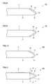
- a nitride semiconductor substrate 10a has an approximately circular shape as seen in plan view and has an orientation flat 12 formed by linearly processing a part of the edge of the outer periphery. Furthermore, on the edge of the outer periphery of nitride semiconductor substrate 10a, a topside chamfer 22 is formed which corresponds to a chamfered portion located on the main surface 11 side. Furthermore, on the outer periphery of a backside surface 21 on the side opposite to main surface 11, a backside chamfer 23 is formed which corresponds to a chamfered portion located on the backside surface 21 side.
- topside chamfer 22 has a width L2 greater than a width L1 of backside chamfer 23.
- Topside chamfer 22 extends in the direction intersecting at an angle ⁇ 2 with the direction in which main surface 11 extends. Furthermore, backside chamfer 23 extends in the direction intersecting at an angle ⁇ 1 with the direction in which backside surface 21 extends. Angles ⁇ 1 and ⁇ 2 may be the same value or a different value.
- a damaged layer 25 is formed on the surface layer of each of topside chamfer 22, backside chamfer 23 and edge face 24. As seen from Fig. 2 , damaged layer 25 formed in topside chamfer 22 has a thickness greater than that of damaged layer 25 formed in backside chamfer 23.
- Main surface 11 corresponds to a plane inclined at an angle of 71° or more and 79° or less with respect to the (0001) plane (c+ plane) toward the [1-100] direction (m+ axis direction) or a plane inclined at an angle of 71° or more and 79° or less with respect to the (000-1) plane (c- plane) toward the [-1100] direction (m- axis direction), and preferably corresponds to the (20-21) plane or the (-202-1) plane. It is to be noted that the plane orientation of main surface 11 may be inclined at a predetermined angle from the above-described plane orientation (20-21) or (-202-1).
- main surface 11 is inclined at an angle ⁇ with respect to the (0001) plane toward the [1-100] direction (m+ axis direction).
- main surface 11 is inclined at angle ⁇ with respect to the [0001] direction (c-axis direction) toward the [1-100] direction (m-axis direction).
- Angle ⁇ is 71° or more and 79° or less, preferably 73° or more and 77° or less, and more preferably 74° or more and 76° or less.
- the m- axis direction herein corresponds to the [-1100] direction.
- the yield of the semiconductor device (for example, a semiconductor laser device) fabricated using this nitride semiconductor substrate 10a can be improved (for example, 50% or more).
- angle ⁇ is 73° or more and 77° or less
- the yield of the semiconductor device (for example, a semiconductor laser device) fabricated using nitride semiconductor substrate 10a can be further improved (for example, 75% or more).
- angle ⁇ is 74° or more and 76° or less
- the yield of the semiconductor device (for example, a semiconductor laser device) fabricated using nitride semiconductor substrate 10a can be still further improved (for example, 80% or more).
- the chamfered portion is inclined at an angle of 5° or more and 45° or less with respect to one, which is adjacent to the chamfered portion, of main surface 11 and backside surface 21 on the side opposite to main surface 11 (angle ⁇ 1 or angle ⁇ 2 in Fig. 2 ).
- the chamfered portion is inclined at an angle of 5° or more and 45° or less with respect to one, which is adjacent to the chamfered portion, of main surface 11 and backside surface 21 on the side opposite to main surface 11 (angle ⁇ 1 or angle ⁇ 2 in Fig. 2 ).
- each of topside chamfer 22 and backside chamfer 23 in the chamfered portion (for example, width L1 and width L2 each corresponding to the chamfering amount) is different between main surface 11 and backside surface 21, main surface 11 and backside surface 21 can be distinguished from each other by visually examining the size of each chamfer.
- the thickness of damaged layer 25 on the main surface 11 side corresponding to the topside surface is different from the thickness of damaged layer 25 on the backside surface 21 side. Accordingly, the stability of the shape of nitride semiconductor substrate 10a can be improved.
- orientation flat 12 is obtained by cutting out a part of the outer periphery of nitride semiconductor substrate 10a in an arcuate shape in order to show the crystal orientation of nitride semiconductor substrate 10a.
- orientation flat 12 corresponds to a linear area formed in a part of the circle of main surface 11 as seen from above.
- the inventors first found that, when the main surface corresponds to the (20-21) plane inclined at an angle of 75° with respect to the (0001) plane toward the [1-100] direction or the (-202-1) plane inclined at an angle of 75° with respect to the (000-1) plane toward the [-1100] direction, cleavage readily occurs at and near the (-1017) plane or the (10-1-7) plane approximately orthogonal to the main surface.
- orientation flat 12 corresponds to the (-1017) plane, the (10-1-7) plane or the plane inclined at angle of-0.5° or more and 0.5° or less from these planes, more preferably corresponds to the (-1017) plane, the (10-1-7) plane or the plane inclined at an angle of -0.2° or more and 0.2° or less from these planes, and most preferably corresponds to the (-1017) plane or the (10-1-7) plane.
- orientation flat 12 is at and near the (-1017) plane or the (10-1-7) plane.
- the (-1017) plane and the (10-1-7) plane are approximately orthogonal to the (20-21) plane or the (-202-1) plane (intersected at an angle of 90.10°). Accordingly, orientation flat 12 is approximately orthogonal to main surface 11.
- These (-1017) plane and (10-1-7) plane each are different from the conventional cleavage plane such as the conventional c-plane, m-plane or a-plane.
- the direction of the normal to the (-1017) plane or the (10-1-7) plane extends approximately in the [-1014] direction or the [10-1-4] direction.
- orientation flat 12 can be readily formed in the plane orthogonal to the [-1014] direction corresponding to the direction of the normal to the (-1017) plane when the main surface is inclined at an angle of 71° or more and 79° or less with respect to the (0001) plane toward the [1-100] direction, or in the plane orthogonal to the [10-1-4] direction corresponding to the direction of the normal to the (10-1-7) plane when the main surface is inclined at an angle of 71° or more and 79° or less with respect to the (000-1) plane toward the [-1100] direction.
- orientation flat 12 can be readily formed in the plane as described above. Furthermore, orientation flat 12 can be readily formed in the (-1017) plane, the (10-1-7) plane, or the plane inclined at an angle of-0.2° or more and 0.2° or less from these planes. In addition, orientation flat 12 may be formed in the (-1017) plane or the (10-1-7) plane.
- the c+ plane represents the (0001) plane having a Ga polarity
- the c- plane represents the (000-1) plane having an N polarity.
- the m-axis direction includes the [1-100] direction, the [10-10] direction, the [-1100] direction, the [-1010] direction, the [01-10] direction, the [0-110] direction, and the direction parallel to these directions.
- the (-1017) plane lies on the side opposite to the (10-1-7) plane.
- Nitride semiconductor substrate 10a is, for example, Al x InyGa (1-x-y) N (0 ⁇ x ⁇ 1,0 ⁇ y ⁇ 1, x + y ⁇ 1), preferably AlxGa (1-x) N (0 ⁇ x ⁇ 1), and more preferably GaN.
- the diameter is preferably 10 mm or more, more preferably 30 mm or more, further preferably 2 inches or more, and still further preferably 3 inches or more.
- the side length is preferably 10 mm or more, more preferably 18 mm or more, and further preferably 30 mm or more.
- the substrate has a thickness of 100 ⁇ m or more and 1000 ⁇ m or less.
- the substrate can be handled when the thickness is 100 ⁇ m or more, and can be cut when the thickness is 1000 ⁇ m or less. It is more preferable that the thickness is 300 ⁇ m or more and 400 ⁇ m or less.
- Fig. 4 the method for manufacturing the nitride semiconductor substrate shown in Figs. 1 and 2 will be described.
- the substrate preparing step (S10) is first carried out. Specifically, in the step (S10), a nitride semiconductor substrate fabricated, for example, by the vapor deposition method is prepared.
- the nitride semiconductor substrate can have an arbitrary planar shape, it may have a circular shape, for example. Furthermore, the nitride semiconductor substrate having a circular shape may have a diameter of 2 inches (approximately 50 mm), for example.
- the nitride semiconductor substrate can be configured to contain dopants to be rendered an arbitrary conductivity type (for example, an n-type). For example, silicon (Si) and oxygen (O) can be applied as dopants that are used for the substrate to be rendered n-type conductivity.
- this step (S10) it is possible to carry out the process step for setting the outer diameter of the ingot of the nitride semiconductor grown, for example, by the vapor deposition method to a predetermined value (for example, outer-periphery grinding step and core-drilling step), and the step of obtaining a wafer by slicing the processed ingot.
- a predetermined value for example, outer-periphery grinding step and core-drilling step
- the nitride semiconductor substrate prepared in this step (S10) may be manufactured by an arbitrary method.
- the nitride semiconductor substrate manufactured by the following method may be prepared.
- the underlying substrate to be prepared may be made of the material identical to or different from that of nitride semiconductor substrate 10a to be grown.
- a GaN substrate for example, a gallium arsenide (GaAs) substrate, a sapphire (Al 2 O 3 ) substrate, a zinc oxide (ZnO) substrate, a silicon carbide (SiC) substrate, and the like can be used.
- a nitride semiconductor crystal is formed on the underlying substrate.
- the method for growing a nitride semiconductor crystal is not particularly limited, but may include the vapor deposition method such as the sublimation method, the HVPE (hydride vapor phase epitaxy) method, the MOCVD (metal organic chemical vapor deposition) method, and the MBE (molecular beam epitaxy) method; and the liquid phase growth method such as the flux method and the ammonothermal method.
- a nitride semiconductor substrate is cut out from the nitride semiconductor crystal processed to achieve an outer diameter having a predetermined value.
- the nitride semiconductor substrate is cut out such that the main surface is inclined at an angle of 71 or more and 79° or less with respect to the (0001) plane toward the [1-100] direction.
- the nitride semiconductor substrate is cut out along the flat plane parallel to main surface 11 in Fig. 3 (the plane inclined at angle ⁇ with respect to the c+ plane toward the m+ axis direction).
- the (0001) plane is on the side opposite to the (000-1) plane, and accordingly, the bottom of the above-mentioned crystal corresponds to the (000-1) plane. Therefore, it is only necessary to cut out the nitride semiconductor substrate such that the main surface is inclined at an angle of 71° or more and 79° or less with respect to that plane toward the [-1100] direction.
- the method for cutting out the nitride semiconductor substrate is not particularly limited, and, for example, a mechanical removal method such as cutting may be employed.
- Cutting means that a slicer provided with an outer peripheral blade, a slicer provided with an inner peripheral blade, a wire saw or the like is used to mechanically cut out nitride semiconductor substrate 10a from the nitride semiconductor crystal.
- the underlying substrate may be removed, if necessary.
- the method for removing the underlying substrate is not particularly limited, for example, a method such as cutting, grinding and the like can be employed.
- Cutting means that a slicer provided with an outer peripheral blade made of an electrodeposited diamond wheel, a wire saw or the like is used to mechanically cut (slice) the interface between the nitride semiconductor crystal and the underlying substrate; to apply or spray a laser pulse or water molecules on the interface between the nitride semiconductor crystal and the underlying substrate; to cause cleavage along the crystal lattice plane, and to mechanically cut apart the nitride semiconductor crystal and the underlying substrate by the chemical method such as etching.
- grinding means that a grindstone is rotated to be brought into contact with the surface of the underlying substrate for scraping in the thickness direction.
- the underlying substrate is mechanically scraped off, for example, by the grinding apparatus provided with a diamond grindstone, and the like.
- the process of fabricating a nitride semiconductor substrate having a main surface inclined at an angle of 71 or more and 79° or less with respect to the (0001) plane toward the [1-100] direction or inclined at an angle of 71° or more and 79° or less with respect to the (000-1) plane toward the [-1100] direction is not limited to the process of cutting out the nitride semiconductor substrate at a desired angle from the nitride semiconductor crystal grown in the c-axis direction.
- a nitride semiconductor substrate can also be manufactured by further growing a nitride semiconductor crystal on the main surface of the nitride semiconductor substrate obtained as described above, cutting out the grown nitride semiconductor crystal along the plane parallel to the main surface of the crystal substrate to produce a nitride semiconductor substrate, and processing the main surface of the nitride semiconductor substrate in the same manner as described above.
- the number of nitride semiconductor substrates used as an underlying substrate for further growing (repeatedly growing) the above-mentioned nitride semiconductor crystal is not necessarily limited to one, but a plurality of crystal substrates of small size may be used.
- the substrates can be joined together during the repeated growth to fabricate a single crystal.
- the crystal substrate cut out from the nitride semiconductor crystal joined during the repeated growth may also be used as an underlying substrate for another repeated growth.
- the production costs can be reduced by repeatedly using and growing the nitride semiconductor crystal.
- a chamfer (chamfered portion) as shown in Fig. 2 is formed at the edge of the outer periphery of nitride semiconductor substrate 10a.
- a rubber grindstone 30 as shown in Figs. 5 and 6 is used to process the edge of the outer periphery of nitride semiconductor substrate 10a.
- rubber grindstone 30 having a surface 31 in the conical shape is used to grind the angular portion of the edge of the outer periphery of nitride semiconductor substrate 10a.
- the area where surface 31 of rubber grindstone 30 is in contact with the edge of nitride semiconductor substrate 10a is linearly formed.
- topside chamfer 22 shown in Fig. 2 is formed.
- rubber grindstone 30 shown in Fig. 5 is rotated, as shown by an arrow in Fig. 5 , about the axis connected to rubber grindstone 30.
- angle ⁇ 2 formed between the direction in which main surface 11 shown in Fig. 2 extends and the direction in which topside chamfer 22 extends can be arbitrarily changed by adjusting the angle formed between surface 31 of rubber grindstone 30 and main surface 11 of nitride semiconductor substrate 10a.
- backside chamfer 23 shown in Fig. 2 can be formed by bringing rubber grindstone 30 shown in Fig. 5 into contact with the edge of nitride semiconductor substrate 10a from the backside surface 21 side and grinding the edge.
- edge face 24 having a curved surface shown in Fig. 2 is obtained by bringing rubber grindstone 30 having a surface 32 formed in a curved shape into contact with the edge face of nitride semiconductor substrate 10a and grinding the edge face.
- rubber grindstone 30 having a grain size for example, of #300 to #3000 may be used.
- this chamfering processing step (S20) a microscope is used to detect the difference of the surface conditions between main surface 11 and backside surface 21 of nitride semiconductor substrate 10a for distinguishing between the topside surface and the backside surface. Then, in this step (S20), the processing amount in each of topside chamfer 22 and backside chamfer 23 is changed (for example, each chamfering amount and angles ⁇ 1 and ⁇ 2 are changed) to allow the topside surface and the backside surface of the substrate to be readily distinguished from each other in the subsequent steps.
- the backside surface grinding step (S30) is carried out.
- backside surface 21 of nitride semiconductor substrate 10a is ground.
- the conventionally well-known arbitrary methods can be employed.
- This step (S30) aims to form nitride semiconductor substrate 10a to have a thickness of a predetermined value.
- the backside surface etching step may be carried out after this step (S30) and before the topside surface grinding step (S40) described below.
- wet etching may be carried out, for example, using KOH as an etching solution. This is carried out in order to remove the damaged layer (for example, having a thickness of 1-30 ⁇ m) formed on the backside surface of the substrate in the step (S30) described above.
- the etching amount is selected as appropriate in accordance with the thickness of the damaged layer.
- the etching amount can be set at 1 ⁇ m or more and 30 ⁇ m or less.
- the topside surface grinding step (S40) is carried out. Specifically, in this step (S40), main surface 11 corresponding to the topside surface of nitride semiconductor substrate 10a is subjected to the grinding process. This grinding process is carried out as a pre-process of the polishing step described below. It is to be noted that the conventionally well-known arbitrary method can be employed in this topside surface grinding step (S40). Furthermore, the thickness of the damaged layer formed in this grinding step is, for example, 0.5 ⁇ m or more and 20 ⁇ m or less.
- the polishing step (S50) is carried out.
- main surface 11 is ground by an arbitrary method. Consequently, main surface 11 can be brought into a mirror-surface state.
- rough polishing and finish polishing may be carried out. This results in formation of a damaged layer on and around main surface 11 (topside surface).
- the thickness of the damaged layer may be 0.1 ⁇ m or more and 5 ⁇ m or less, though varying depending on the conditions.
- the etching step (S60) is carried out.
- this step (S60) at least a part of the damaged layer in each of main surface 11 and the chamfered portion of nitride semiconductor substrate 10a is removed by etching.
- An arbitrary method can be used as an etching method, and, for example, dry etching may be used.
- this step (S60) while the damaged layer of main surface 11 is completely removed, the damaged layer in the peripheral portion corresponding to the chamfered portion may be remained to have a thickness of 1 ⁇ m or more and 3 ⁇ m or less.
- this etching step (S60) is not necessarily carried out.
- the roughness of the main surface of the nitride semiconductor substrate is 10 nm or less in terms of Ra standards.
- the roughness of the backside surface is 10 ⁇ m or less in terms of Ra standards.
- the step of forming orientation flat 12 may be carried out before or after the step (S20).
- the method for forming orientation flat 12 is not particularly limited, the nitride semiconductor substrate is subjected, for example, to cutting, grinding and the like in order to expose the (-1017) plane, the (10-1-7) plane, or the plane inclined at an angle of -0.5° or more and 0.5° or less from these planes.
- nitride semiconductor substrate 10a shown in Figs. 1 and 2 can be obtained.
- nitride semiconductor substrate 10a shown in Figs. 1 and 2 is basically similar in structure to nitride semiconductor substrate 10a shown in Figs. 1 and 2 , but is different in shape of edge face 24.
- nitride semiconductor substrate 10a shown in Fig. 7 is provided with edge face 24 having a linear cross section as shown in Fig. 7 .
- the substrate having such a configuration also allows the effects similar to those of nitride semiconductor substrate 10a shown in Figs. 1 and 2 to be obtained.
- nitride semiconductor substrate 10a shown in Figs. 1 and 2 is basically similar in structure to nitride semiconductor substrate 10a shown in Figs. 1 and 2 , but is different in shape of damaged layer 25 in the chamfered portion.
- damaged layer 25 is formed only in topside chamfer 22.
- the substrate of such a configuration also allows the effects similar to those of nitride semiconductor substrate 10a shown in Figs. 1 and 2 to be obtained.
- Nitride semiconductor substrate 10a shown in Fig. 9 is basically similar in structure to nitride semiconductor substrate 10a shown in Figs. 1 and 2 , but is different in shape of the chamfered portion.
- the width of backside chamfer 23 (the chamfering amount) is greater than the width of topside chamfer 22 (the chamfering amount) forming a chamfered portion.
- the substrate of the above-described configuration also allows the effects similar to those of nitride semiconductor substrate 10a shown in Figs. 1 and 2 to be obtained.
- Nitride semiconductor substrate 10a shown in Fig. 10 is another modification of nitride semiconductor substrate 10a shown in Figs. 1 and 2 , but is different in shape of the chamfered portion from nitride semiconductor substrate 10a shown in Figs. 1 and 2 .
- the contour of the cross section of each of topside chamfer 22, backside chamfer 23 and edge face 24 constituting a chamfered portion has a curved shape.
- the substrate of the above-described configuration also allows the effects similar to those of nitride semiconductor substrate 10a shown in Figs. 1 and 2 to be obtained.
- Nitride semiconductor substrate 10a shown in Fig. 11 is basically similar in configuration to nitride semiconductor substrate 10a shown in Figs. 1 and 2 , but is different in shape of the chamfered portion from nitride semiconductor substrate 10a shown in Figs. 1 and 2 .
- topside chamfer 22 and backside chamfer 23 are almost equal in width.
- the substrate of the above-described configuration also allows the effects similar to those of nitride semiconductor substrate 10a shown in Fig. 1 to be obtained, for example, such as prevention of cracking and chipping occurring from the edge of the substrate.
- topside chamfer 22 and backside chamfer 23 are almost equal in width, the warpage of the nitride semiconductor substrate can be reduced.
- FIG. 12 and 13 another modification of the nitride semiconductor substrate shown in Figs. 1 and 2 will be described.
- a nitride semiconductor substrate 10b shown in Fig. 12 is basically similar in configuration to nitride semiconductor substrate 10a shown in Figs. 1 and 2 , but is different from nitride semiconductor substrate 10a in that nitride semiconductor substrate 10b further includes a second orientation flat 13.
- Second orientation flat 13 serves as an IF (identification flat) or a sub-orientation flat for providing an indication of an orientation and for distinguishing between the topside surface and the backside surface. Second orientation flat 13 is approximately orthogonal to orientation flat 12. Second orientation flat 13 corresponds to the (11-20) plane (a-plane) or the plane inclined at an angle of-0.5° or more and 0.5° or less from this plane, and more preferably, corresponds to the (11-20) plane.
- second orientation flat 13 is at or near the (11-20) plane.
- the (11-20) plane is approximately orthogonal to the (20-21) plane or the (-202-1) plane, and also approximately orthogonal to the (-1017) plane or the (10-1-7) plane.
- Second orientation flat 13 also allows the (11-20) plane or the plane inclined at an angle of-0.5° or more and 0.5° or less from this plane to be specified. It also allows the topside surface and the backside surface of nitride semiconductor substrate 10b to be readily distinguished from each other. Furthermore, cleavage readily occurs at and near the (11-20) plane where second orientation flat 13 can therefore readily be provided. In the case where second orientation flat 13 is at or near the (11-20) plane, the yield of the semiconductor device can be further improved.
- the a-plane as described above includes and is equivalent to the (11-20) plane, the (1-210) plane, the (-2110) plane, the (-1-120) plane, the (-12-10) plane, the (2-1-10) plane, and the plane parallel to these planes.
- the [1-210] direction and the [-12-10] direction in Fig. 3 extend in the a-axis direction.
- the a-axis direction includes the [11-20] direction, the [1-210] direction, the [-2110] direction, the [-1-120] direction, the [-12-10] direction, the [2-1-10] direction, and the direction parallel to these directions.
- a length L12 of orientation flat 12 is different from a length L13 of second orientation flat 13. It is more preferable that these lengths are different enough to allow the difference between the lengths to be visually distinguished.
- orientation flat 12 has length L12 of, for example, 2 mm or more and 30 mm or less
- second orientation flat 13 has length L13 shorter than length L12 and of 2 mm or more and 20 mm or less, for example.
- lengths L12 and L13 of orientation flat 12 and second orientation flat 13, respectively, correspond to each length of the linear areas in nitride semiconductor substrate 10b as seen from above.
- the method for manufacturing the nitride semiconductor substrate shown in Fig. 12 is basically similar in configuration to the method for manufacturing the nitride semiconductor substrate shown in Figs. 1 and 2 , but is different in that it further includes the step of forming second orientation flat 13. Specifically, second orientation flat 13 corresponding to the (11-20) plane or the plane inclined at an angle of-0.5° or more and 0.5° or less from this plane is formed before, after or at the same time as formation of orientation flat 12.
- nitride semiconductor substrate 10b according to the present embodiment further includes second orientation flat 13 corresponding to the (11-20) plane or the plane inclined at an angle of -0.5° or more and 0.5° or less from this plane.
- Cleavage tends to occur in the plane (11-20) or the plane inclined at an angle of -0.5° or more and 0.5° or less from this plane, where second orientation flat 13 can therefore readily be formed. This also allows the topside surface and the backside surface of nitride semiconductor substrate 10b to be distinguished from each other.
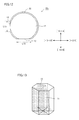
- a nitride semiconductor substrate 10c shown in Figs. 14 and 15 is basically similar in configuration to nitride semiconductor substrate 10a shown in Figs. 1 and 2 , but is different in that it includes a notch 15 as an indicator.
- Notch 15 is a cutout portion provided at the outer periphery of nitride semiconductor substrate 10c. As shown in Figs. 14 and 15 , notch 15 is provided in order to specify the (-1017) plane, the (-1017) plane, or the plane inclined at an angle of-0.5° or more and 0.5° or less from these planes. Specifically, as shown in Fig. 15 , when three points A, B and C are positioned in notch 15, the direction extending from the intermediate point between points B and C to point A corresponds to the [-1014] direction or the [10-1-4] direction.
- a depth H of notch 15 is, for example, 2 mm or more and 10 mm or less, and an angle ⁇ is 30° or more and 120° or less.
- an angle ⁇ is 30° or more and 120° or less.
- the area of main surface 11 of nitride semiconductor substrate 10c can be prevented from being reduced.
- notch 15 can readily be identified.
- the method for manufacturing nitride semiconductor substrate 10c shown in Figs. 14 and 15 is basically similar in configuration to the method for manufacturing nitride semiconductor substrate 10a shown in Figs. 1 and 2 , but is different in that notch 15 is provided in place of orientation flat 12.
- the method for providing notch 15 is not particularly limited, but notch 15 can be provided by cutting, grinding, polishing, and the like.
- FIG. 16 another modification of the nitride semiconductor substrate shown in Figs. 1 and 2 will be hereinafter described.
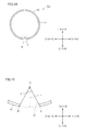
- a nitride semiconductor substrate 10d shown in Fig. 16 is basically similar in structure to nitride semiconductor substrate 10c shown in Figs. 14 and 15 , but is different from nitride semiconductor substrate 10c shown in Figs. 14 and 15 in that a second notch 16 is provided.
- Second notch 16 is provided in order to provide an indication of an orientation and to distinguish between the topside surface and the backside surface.
- the direction of second notch 16 is approximately orthogonal to the direction of notch 15.
- Second notch 16 serves to indicate the (11-20) plane or the plane inclined at an angle of-0.5° or more and 0.5° or less from this plane, and more preferably, serves to indicate the (11-20) plane.
- notch 15 and second notch 16 can be distinguished from each other in that notch 15 corresponds to a main notch and second notch 16 corresponds to a sub-notch.
- notch 15 may be greater than second notch 16 for the purpose of distinguishing them from each other.
- the method for manufacturing nitride semiconductor substrate 10d shown in Fig. 16 is basically similar in configuration to the method for manufacturing nitride semiconductor substrate 10c shown in Figs. 14 and 15 , but is different in that second notch 16 is further provided.
- a nitride semiconductor substrate 10e shown in Fig. 17 is basically similar in configuration to nitride semiconductor substrate 10a shown in Figs. 1 and 2 , but is different in that a mark 17 is provided as an indicator.
- Mark 17 is provided, for example, by application of a laser beam or by scratching by a diamond pen. Mark 17 is provided such that the (-1017) plane, the (10-1-7) plane, or the plane inclined at an angle of-0.5° or more and 0.5° or less from these planes can be specified. For example, a plurality of marks 17 are provided in parallel with the [10-1-4] direction, the [-1014] direction or the direction inclined at an angle of -0.5° or more and 0.5° or less from these directions.
- mark 17 is provided so as to allow the (11-20) plane or the plane inclined at an angle of -0.5° or more and 0.5° or less from this plane to be specified.
- mark 17 in the [-1014] or [10-1-4] direction is provided to vary in size, number and the like from mark 17 in the [11-20] direction.
- the number of marks 17 is greater in the [11-20] direction than in the [-1014] direction. Consequently, the [-1014] direction and the [11-20] direction can be identified.
- marks 17 are provided in one place as a plurality of dots in Fig. 17 , marks 17 may be provided in two or more regions, a single mark 17 may be provided, and mark 17 may have a shape other than a dot.
- mark 17 is provided in the plane on the side opposite to the plane used for epitaxial growth in nitride semiconductor substrate 10e. Even in the case where mark 17 is provided in the backside surface and an impermeable metal film and the like are formed, since the nitride semiconductor has light transmissivity, its main surface is subjected to the polishing process to thereby allow mark 17 provided in the backside surface to be readily recognized.
- the method for manufacturing nitride semiconductor substrate 10e according to the present embodiment is basically similar in configuration to nitride semiconductor substrate 10a shown in Figs. 1 and 2 , but is different in that mark 17 is provided in place of orientation flat 12.
- mark 17 is not particularly limited, for example, the method for providing a laser beam irradiation mark by applying a laser beam or the method for providing a mark made by scratching by a diamond pen may be employed. Consequently, mark 17 can readily be provided. Mark 17 can also be provided with an improved processing accuracy.
- orientation flat 12, notch 15 and mark 17 have been described by way of an example of an indicator with regard to the above-described nitride semiconductor substrates 10a-10e, the indicator of the nitride semiconductor substrate of the present invention is not particularly limited thereto. Furthermore, the nitride semiconductor substrate of the present invention may include an orientation flat, a notch, a mark, and the like in combination.
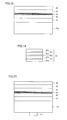
- the light emitting element includes a nitride semiconductor substrate 10a corresponding to a GaN substrate of n-type conductivity, an n-type GaN layer 41, an AlGaN layer 42 formed on n-type GaN layer 41, a light emitting layer 43 formed on AlGaN layer 42, a p-type AlGaN layer 44 formed on light emitting layer 43, and a p-type GaN layer 45 formed on p-type AlGaN layer 44.
- Nitride semiconductor substrate 10a which is an n-type GaN substrate exhibits characteristics, for example, having a resistance value of 1 ⁇ 10 -2 ⁇ cm and a concentration of the n-type conductive impurities of 3 ⁇ 10 18 /cm 3
- n-type GaN layer 41 can be configured to have a thickness of 1 ⁇ m.
- silicon (Si) can be used as conductive impurities contained in this n-type GaN layer.
- n-type AlGaN layer 42 can be configured to have a thickness of 150 nm.
- silicon can be used as conductive impurities contained in this n-type AlGaN layer 42.
- AlGaN layer 42 may have composition of Al 0 . 1 Ga 0 . 9 N, for example.
- light emitting layer 43 may have a multilayer structure obtained by alternately laminating GaN layer 43 a and GaInN layer 43b.
- GaN layer 43a and GaInN layer 43b may be configured to have thicknesses of 10 nm and 3 nm, respectively.
- Ga 0 . 85 In 0 . 15 N can be used as composition of the GaInN layer.
- P-type AlGaN layer 44 located on this light emitting layer 43 can be configured to have a thickness of 20 nm. Furthermore, magnesium (Mg) can be used as conductive impurities contained in this p-type AlGaN layer. For example, Al 0.2 Ga 0.8 N can be used as composition of this p-type AlGaN layer 44.
- p-type GaN layer 45 can be configured to have a thickness of 150 nm. Also, magnesium can be used as conductive impurities contained in this p-type GaN layer 45.
- the semiconductor element shown in Figs. 18 and 19 can be formed by carrying out the steps of preparing one of nitride semiconductor substrates 10a-10e according to the present invention by using the method for manufacturing the substrate shown in Fig. 4 , and then, epitaxially growing a predetermined film on main surface 11 of one of nitride semiconductor substrates 10a-10e.
- an electrode is formed on the topside surface and the backside surface of the semiconductor element shown in Figs. 18 and 19 .
- a p-side electrode 46 is formed on p-type GaN layer 45.
- the electrode having a laminated structure of nickel (Ni) and gold (Au) can be used as this p-side electrode 46.
- an electrode having a laminated structure made of titanium (Ti)/aluminum (Al)/titanium (Ti)/gold (Au) can be used as an n-side electrode 47, as shown in Fig. 20 .
- N-side electrode 47 is located approximately in the center of the surface of nitride semiconductor substrate 10a.
- P-side electrode 46 is formed so as to cover the surface of p-type GaN layer 45.
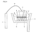
- the light emitting element fabricated in this way is attached to a stem as shown in Fig. 21 to allow formation of a light emitting device.
- p-side electrode 46 of the light emitting element shown in Fig. 20 is fixedly connected to a stem 52 by solder 53.
- n-side electrode 47 is electrically connected to a lead pin 51 through a wire 54.
- the GaN substrate also has a high heat conductivity, which causes heat to be dissipated also from the substrate side.
- the light emitting element can be configured to have a light emission wavelength of 430 nm to 550 nm.
- the light emission wavelength can be adjusted by the In composition of the light emitting layer.
- the efficiency of taking in of In during the epitaxial growth can be improved, and thus, an excellent light emitting property can be achieved at a light emission wavelength of 500 nm to 550 nm in the green region.
- Nitride semiconductor substrates 10a-10e includes main surface 11 inclined at an angle of 71° or more and 79° or less with respect to the (0001) plane toward the [1-100] direction or inclined at an angle of 71° or more and 79° or less with respect to the (000-1) plane toward the [-1100] direction; and a chamfered portion located at the edge of the outer periphery of main surface 11.
- the chamfered portion is inclined at an angle ( ⁇ 1 or ⁇ 2) of 5° or more and 45° or less with respect to one, which is adjacent to the chamfered portion, of main surface 11 and backside surface 21 on the side opposite to main surface 11.
- Nitride semiconductor substrates 10a-10e according to the present invention each have main surface 11 which allows the yield to be improved at the time when a semiconductor device is fabricated.
- cracking and chipping occurring from the edge of the outer periphery of nitride semiconductor substrates 10a-10e can be suppressed. Consequently, defects occurring in nitride semiconductor substrates 10a-10e resulting from the above-mentioned cracking and chipping can be suppressed, and the yield of nitride semiconductor substrates 10a-10e can also be improved.
- main surface 11 is inclined at an angle of 71° or more and 79° or less with respect to the (0001) plane toward the [1-100] direction or inclined at an angle of 71° or more and 79° or less with respect to the (000-1) plane toward the [-1100] direction as described above since the yield of the semiconductor device can be improved particularly in this angle range. Furthermore, the lower limit of inclination angle ⁇ 1 or ⁇ 2 of the chamfered portion is set at 5°.
- the angle is smaller than this lower limit, the resultant angular portion at the edge of the outer periphery of the substrate is almost the same as that obtained in the case where no chamfered portion is substantially formed, with the result that no effect of suppressing cracking and chipping can be achieved.
- the upper limit of the inclination angle is set at 45°. This is because, when the angle is greater than this upper limit, the resultant angular portion of the interface between the chamfered portion and the main surface shows an angle smaller than 135°, which produces a problem of cracking and chipping in this angular portion.
- the inclination angle of the chamfered portion as described above is preferably 15° or more and 35° or less, and more preferably, 17° or more and 25° or less.
- the reason why the value range is set as described above is that it can increase the probability of preventing cracking, fracturing and chipping occurring in the subsequent steps (the topside surface grinding and backside surface grinding steps).
- main surface 11 may be inclined at an angle of -0.5° or more and 0.5° or less from the (20-21) plane or the (-202-1) plane.
- each of nitride semiconductor substrates 10a-10e having the above-mentioned plane as main surface 11 is used to fabricate a semiconductor device, which allows its characteristics to be particularly improved.
- a damaged layer 25 having an average thickness of 0.5 ⁇ m or more and 10 ⁇ m or less may be formed on the surface layer of the chamfered portion.
- damaged layer 25 is formed at the edge of the outer periphery of each of nitride semiconductor substrates 10a-10e to thereby allow the region having remaining stress to be provided at the edge of the outer periphery. Consequently, the effects of reducing defects in shape such as warpage of nitride semiconductor substrates 10a-10e can be achieved by adjusting the thickness of damaged layer 25 as appropriate.
- the average thickness of damaged layer 25 can be measured by a TEM (transmission electron microscope).
- the lower limit of the average thickness is set at 0.5 ⁇ m since, when forming a chamfered portion by polishing and grinding, the damaged layer having a thickness less than 0.5 ⁇ m causes reduction in effects of suppressing warpage, which leads to a decrease in the yield of the device.
- the upper limit of the average thickness is set at 10 ⁇ m since the damaged layer formed to have a thickness greater than 10 ⁇ m causes an increase in probability of occurrence of cracking and fracturing, which leads to a further decrease in the yield of the device.
- the average thickness of damaged layer 25 is preferably 1 ⁇ m or more and 5 ⁇ m or less.
- the reason why the value range is set as described above is that the grindstone of a large grain size is used in the process where the average thickness is 1 ⁇ m or less, which increases the processing time to cause an increase in manufacturing costs, and that the grindstone of a small grain size (coarser) is used in the process where the average thickness is 5 ⁇ m or more, which causes a decrease in the yield of the device due to problems such as generation of particles.
- the chamfering amount of the chamfered portion may be 0.02 mm or more and 0.5 mm or less. In this case, the effects of suppressing cracking and chipping occurring from the edge of the outer periphery of each of nitride semiconductor substrates 10a-10e can be reliably achieved.
- the lower limit of the chamfering amount is set at 0.02 mm. This is because, when the value is smaller than this lower limit, the resultant angular portion at the edge of the outer periphery of the substrate is almost the same as that obtained in the case where no chamfered portion is substantially formed, with the result that no effect of suppressing cracking and chipping can be achieved.
- the upper limit of the chamfering amount is set at 0.5 mm. This is because, when the chamfering amount is greater than this upper limit, the area of the chamfered portion is excessively increased in the main surface of the substrate to thereby cause a decrease in the number of semiconductor devices obtained from the substrate, which results in an increase in manufacturing costs of the semiconductor device.
- the above-described chamfering amount is preferably 0.05 mm or more and 0.3 mm or less, and more preferably, 0.05 mm or more and 0.2 mm or less.
- the reason why the value range is set as described above is that a greater chamfering amount (leading to an increase in the grinding amount) causes an increased load to be applied to the substrate during processing, which leads to an increase in the probability of occurrence of defects such as cracking and the like.
- the arithmetical mean roughness (Ra) in the topside surface of the chamfered portion may be 0.07 ⁇ m or more and 3 ⁇ m or less.
- the lower limit of the above-mentioned surface roughness is set at 0.07 ⁇ m in terms of Ra since it is difficult to reduce the surface roughness below this lower limit at reasonable costs.
- the upper limit of the above-mentioned surface roughness is set at 3 ⁇ m in terms of Ra since the value greater than this upper limit causes an increased probability of occurrence of problems such as generation of particles.
- the above-mentioned surface roughness is, in terms of Ra, preferably 0.07 ⁇ m or more and 1 ⁇ m or less, and more preferably, 0.07 ⁇ m or more and 0.5 ⁇ m or less.
- the reason why the value range is set as described above is that the smaller the Ra is, the finer the particles (impurities) can be suppressed from occurring, which leads to an increase in the yield of the device element.
- main surface 11 may be subjected to mirror-surface processing.
- the surface roughness of main surface 11 may be 0.2 nm or more and 4 nm or less in terms of the root mean square roughness (RMS).
- the lower limit of the surface roughness of main surface 11 is set at the above-described values since it is difficult to set the surface roughness below the above-described values at industrially reasonable costs. Furthermore, the upper limit of the above-described surface roughness is set at the above-described values since the value greater than the above-described values causes an increased probability of occurrence of formation defects in the epitaxial film.
- the above-described surface roughness of main surface 11 is preferably 1 nm or more and 3 nm or less in terms of RMS.
- the reason why the value range is set as described above is that this value range is preferable in terms of costs and quality as with the reasons described above.
- An indicator (orientation flats 12 and 13, notches 15 and 16, mark 17) indicating a predetermined plane may be provided in the above-described nitride semiconductor substrates 10a-10e.
- nitride semiconductor substrates 10a-10e are treated or when nitride semiconductor substrates 10a-10e are used to manufacture a semiconductor device (see Figs. 18-21 ), the plane orientation of each of nitride semiconductor substrates 10a-10e can be reliably recognized.
- the predetermined plane indicated by the indicator may be the (-1017) plane, the (10-1-7) plane, or the plane inclined at an angle of -0.5° or more and 0.5° or less from these planes, or may be the (11-20) plane or the plane inclined at an angle of -0.5° or more and 0.5° or less from this plane.
- Nitride semiconductor substrates 10a-10e according to the present invention each have main surface 11 that allows the yield to be improved when a semiconductor device is fabricated.
- the inventors of the present invention found that the (-1017) plane and the (10-1-7) plane and their vicinities tend to readily cleave. Then, the inventors first revealed that the (-1017) plane, the (10-1-7) plane, or the plane inclined at an angle of -0.5° or more and 0.5° or less from these planes is identified by the indicator.
- This indicator allows the plane to be specified, which is readily cleaved when fabricating a semiconductor device using nitride semiconductor substrates 10a-10e each having this main surface 11. Accordingly, the crystal orientation can be aligned or distinguished by using the plane that is readily cleaved. Thus, a semiconductor device exhibiting improved characteristics can be fabricated by using nitride semiconductor substrates 10a-10e according to the present invention. Therefore, nitride semiconductor substrates 10a-10e according to the present invention can be used for a semiconductor device.
- the method for manufacturing a nitride semiconductor substrate according to the present invention includes the step (S10) of preparing a nitride semiconductor substrate having a main surface inclined at an angle of 71° or more and 79° or less with respect to the (0001) plane toward the [1-100] direction or inclined at an angle of 71° or more and 79° or less with respect to the (000-1) plane toward the [-1100] direction; and the step (S20) of chamfering the edge of the outer periphery of the main surface of the nitride semiconductor substrate.
- the step (S20) of chamfering the edge includes the step of forming a chamfered portion inclined at an angle ( ⁇ 1 or ⁇ 2) of 5° or more and 45° or less with respect to one, which is adjacent to the chamfered portion, of main surface 11 and backside surface 21 on the side opposite to main surface 11.
- ⁇ 1 or ⁇ 2 an angle of 5° or more and 45° or less with respect to one, which is adjacent to the chamfered portion, of main surface 11 and backside surface 21 on the side opposite to main surface 11.
- the semiconductor device according to the present invention is fabricated using each of the above-described nitride semiconductor substrates 10a-10e, as shown in Figs. 18-21 .
- a semiconductor device exhibiting a high manufacturing yield can be implemented.
- the method for manufacturing a semiconductor device includes the steps of preparing nitride semiconductor substrates 10a-10e using the method for manufacturing the above-described nitride semiconductor substrate as shown in Fig. 4 ; and forming an epitaxial layer on main surface 11 of each of nitride semiconductor substrates 10a-10e.
- a semiconductor device exhibiting a high manufacturing yield can be implemented.
- the usability of the GaN substrate cut out from the (0001) GaN ingot in the [1-100] direction at an angle ⁇ in the range between 68° and 82° was examined (Test 1). Specifically, the substrate with an angle different from angle ⁇ was used to form an element of a semiconductor laser device and measure the oscillation yield of the element. Furthermore, an examination was made with regard to the effects of the inclination angle ( ⁇ 1 or ⁇ 2) of the chamfered portion with respect to adjacent one of main surface 11 and backside surface 21 on the side opposite to main surface 11 (Test 2).
- the (0001) GaN ingot thickly grown by the HVPE method was cut at an angle ⁇ in the range between 68° and 82° in the [1-100] direction using a wafer slicing apparatus to fabricate a GaN substrate (sample IDs in Table 1 set forth below: I-1 to I-9) in which an inclination angle ⁇ formed between the [0001] direction and the [1-100] direction has a desired off angle in the range between 68° and 82°.
- a GaN substrate having the (20-21) plane as a main surface was obtained. This main surface corresponds to main surface 11 in the hexagonal crystal lattice in Fig. 3 .
- a chamfered portion was formed at its edge of the outer periphery.
- fracturing or cracking may occur from the outer periphery of the GaN substrate.
- a rubber grindstone was used for processing in order to prevent fracturing and cracking.
- the outer periphery was ground using a grindstone in which a mixture of 40 wt% of diamond abrasive grains having a grain size of #1000 and 60 wt% of Fe 2 O 3 abrasive grains was fixed to the base with CR (chloroprene rubber).
- the arithmetical mean roughness (Ra) of the topside surface was 0.1 ⁇ m.
- the rubber grindstone has a porosity of 0% and has a thickness equal to that of the substrate.
- the shape of the chamfered portion was formed based on the shape shown in Fig. 11 in which the shapes on the topside and the backside were symmetrical to each other.
- the angle of the chamfer was uniformly set at 20°, and the chamfering amount was uniformly set at 0.2 mm.
- the remaining length is also determined, and accordingly, the chamfers can be connected to each other by a smooth curved surface.
- the GaN substrate was used to form a semiconductor laser device by the metal organic chemical vapor deposition method.
- a resultant semiconductor laser device 100 has a configuration shown in Figs. 22 and 23 .
- the materials used in the metal organic chemical vapor deposition method include trimethyl gallium (TMGa), trimethyl aluminum (TMAl), trimethyl indium (TMIn), ammonia (NH 3 ), and silane (SiH 4 ).
- n-type GaN having a thickness of 1000 nm was grown as an n-type buffer layer 102 on the main surface of nitride semiconductor substrate 10a (GaN substrate).
- an n-type InAlGaN cladding layer having a thickness of 1200 nm was grown as an n-type cladding layer 103.
- an n-type GaN guide layer having a thickness of 200 nm as an n-type guide layer 104 and an undoped InGaN guide layer having a thickness of 65 nm as an undoped guide layer 105 were grown.
- a 3-cycle MQW structure made of GaN having a thickness of 15 nm and InGaN having a thickness of 3 nm was grown as an active layer 106.
- an undoped InGaN guide layer having a thickness of 65 nm as an undoped guide layer 107, a p-type AlGaN block layer having a thickness of 20 nm as a p-type block layer 108, and a p-type GaN guide layer having a thickness of 200 nm as a p-type guide layer 109 were grown.
- a p-type InAlGaN cladding layer having a thickness of 400 nm was grown as a p-type cladding layer 110.
- a p-type GaN contact layer having a thickness of 50 nm was grown as a p-type contact layer 111.
- the photolithography method was used to provide a stripe window having a width of 10 ⁇ m in insulation film 112 by wet etching.
- the direction of the laser stripe was inclined at an angle of -0.5° or more and 0.5° or less from the [-1014] direction, as shown in Fig. 23 .
- the orientation of a waveguide 100c of semiconductor laser device 100 is in the [-1014] direction or is inclined at an angle of -4° or more and 4° or less with respect to this direction toward the [1-100] direction, and is inclined at an angle of-0.5° or more and 0.5 ° or less in the direction orthogonal to the [1-100] direction, as shown in Fig. 23 .
- waveguide 100c is formed in the direction approximately vertical to end faces 100a and 100b (the (-1017) plane, the (10-1-7) plane, or the plane inclined at an angle of -4° or more and 4° or less with respect to these planes toward the [1-100] direction and inclined at an angle of-0.5° or more and 0.5° or less in the direction orthogonal to the [1-100] direction).
- a p-type electrode 113 made of Ni/Au and a pad electrode (not shown) made of Ti/Al were vapor-deposited.
- the backside surface of the GaN substrate (nitride semiconductor substrate 10a) was ground to achieve a substrate thickness of 100 ⁇ m or less which facilitates cleavage, and fabricate a substrate product having a backside surface in the mirror state.
- an n-type electrode 114 made of Ti/Al/Ti/Au was formed by vapor deposition.
- a resonator mirror for this laser stripe was fabricated using a laser scriber employing a YAG laser beam having a wavelength of 355 nm.
- the oscillation chip yield can be improved as compared to the case where the diamond scribe method is used.
- a scribe groove was formed on the conditions that the laser light output was set at 100 mW and the scanning speed was set at 5 mm/s.
- the resultant scribe groove had a length of 30 ⁇ m, a width of 10 ⁇ m and a depth of 40 ⁇ m.
- the scribe groove was formed by directly applying a laser light beam to the surface of the epitaxial layer at a pitch of 800 ⁇ m through an opening in the insulation film of the GaN substrate.
- the resonator length was set at 600 ⁇ m.
- a resonator mirror was fabricated by cutting using a blade. The blade was pressed against the underside of the GaN substrate to cut the substrate product, thereby fabricating a laser bar. More specifically, as shown in Fig. 24 , end faces 100a and 100b for a laser resonator correspond to the (-1017) plane and the (10-1-7) plane, respectively. Main surface 11, end faces 100a and 100b are different from the conventional cleavage plane such as the conventional c-plane, m-plane and a-plane, respectively.
- the degree of flatness of the plane obtained by cutting is 20 nm or less. Furthermore, the vertical degree with respect to the sample surface of the above-described plane fell within a range of ⁇ 5°.
- the end face of the laser bar was coated with a dielectric multilayer film by the vacuum deposition method.
- the dielectric multilayer film was formed by alternately laminating SiO 2 (silicon oxide) and TiO 2 (titanium dioxide). The film thickness was adjusted to fall within a range of 50 nm or more and 100 nm or less, to design the center wavelength of the reflectivity to fall within a range of 500 nm or more and 530 nm or less.
- the reflecting plane was set to 10 cycles and the design value of the reflectivity was set at about 95%.
- the reflecting plane was set to 6 cycles and the design value of the reflectivity was set at about 80%.
- Table 1 shows that excellent results were obtained in that the oscillation yield was 50% or more when inclination angle ⁇ of the GaN substrate formed between the [0001] direction and the [1-100] direction (the angle of the main surface described in Table 1) fell within a range of 71° or more and 79° or less.
- Test 2 an experiment was made basically with regard to the substrate having the above-described inclination angle ⁇ (the angle of the main surface) of 75°. Specifically, the element yield and the substrate yield were examined with the topside and backside surfaces at different angles.
- the substrate yield which corresponds to the percentage by which the substrate suffers no cracking, fracturing and chipping, was defined as (the number of substrates suffering no cracking, fracturing and chipping observed by visual confirmation)/(the number of the measured substrates).
- Samples of the GaN substrate (sample IDs in Table 2 described below: II-1 to II-11) and samples of the semiconductor laser device were fabricated by the method basically similar to that used for fabricating the samples prepared in Test 1 as described above.
- the angle of the main surface (inclination angle ⁇ ) was set at 75°, 71° or 79°.
- the chamfered angle of the chamfered portion was changed in the range of 0° to 60°, as shown in Table 2.
- the grindstone having a grain size of #1000 was used for chamfering.
- the substrate having the same thickness was used.
- the shape of the chamfered portion (chamfer shape) was formed based on the shape shown in Fig. 11 in which the shapes on the topside and the backside were symmetrical to each other.
- the chamfering amount was uniformly set at 0.2 mm.
- the substrate yield was calculated by visually observing the situation in which defects such as cracking, fracturing and chipping occur. Furthermore, with regard to the semiconductor laser device fabricated using each sample of the GaN substrate, the oscillation yield (element yield) was measured in the same manner as in Test 1. The results are shown in Table 2.
- the excellent results were obtained in that the substrate yields was 50% or more when the chamfered angle was 5° or more and 45° or less. Furthermore, the similar results were obtained also when using the chamfered portion having the chamfering amount and the chamfered angle each different between the topside surface and the backside surface.
- the substrate having a damaged layer of a different thickness in the chamfered portion was used to examine the effects caused by the thickness of the damaged layer. Specifically, samples of the GaN substrate having a damaged layer of a different thickness in the chamfered portion were prepared. Then, a semiconductor laser device having the same structure as in Example 1 was fabricated using the GaN substrate, and the element yield was examined.
- Samples of the GaN substrate (sample IDs in Table 3 described below: III-1 to III-9) were fabricated basically by the same manufacturing method as that of the GaN substrate in Example 1.
- the thickness of the damaged layer was changed by adjusting the grain size and the like of the rubber grindstone used for chamfering processing.
- the GaN substrate was configured to have a main surface inclined at angle ⁇ (angle of the main surface) of 75° or 73° with respect to the (0001) plane toward the [1-100] direction.
- the resultant GaN substrate was used to fabricate a semiconductor laser device as in Example 1. Furthermore, the substrate having the same thickness was used, and the shape of the chamfered portion (chamfer shape) was formed based on the shape shown in Fig. 11 in which the shapes on the topside and the backside were symmetrical to each other.
- the chamfered angle was uniformly set at 20° and the chamfering amount was uniformly set at 0.2 mm.
- the excellent results were obtained in that the element yields was 50% or more when the average damaged layer thickness in the chamfer was 0.5 ⁇ m or more and 10 ⁇ m or less. Furthermore, the same results were obtained also when using the chamfered portion having the chamfering amount and the chamfered angle each different between the topside surface and the backside surface. Also with regard to the crystal grown by the flux method, the same results as those described above were obtained. Furthermore, the same results as those described above were obtained also when a plurality of GaN substrates were used for an underlying substrate to grow a single GaN crystal on the plurality of underlying substrates by the HVPE method.
- the substrate having a chamfered portion chamfered by a different amount was used to examine the effects caused by the chamfering amount.
- samples of the GaN substrate having a chamfered portion chamfered by a different amount were prepared to examine the substrate yield.
- Samples of the GaN substrate were fabricated basically by the same manufacturing method as that of the GaN substrate in Example 1.
- Inclination angle ⁇ of the main surface of the GaN substrate (angle of the main surface) with respect to the (0001) plane toward the [1-100] direction was set at 75° or 74°.
- the grindstone having a grain size of #1000 was used for chamfering.
- the substrate having the same thickness was used, and the shape of the chamfered portion (chamfer shape) was formed based on the shape shown in Fig. 11 in which the shapes on the topside and the backside were symmetrical to each other.
- the chamfered angle was uniformly set at 20°.
- the excellent results were obtained in that the substrate yields was 50% or more when the chamfering amount was 0.02 mm or more and 0.5 mm or less. Furthermore, the same results were obtained also when using the chamfered portion having the chamfering amount and the chamfered angle each different between the topside surface and the backside surface. Also with regard to the crystal grown by the flux method, the same results as those described above were obtained. Furthermore, the same results as those described above were obtained also when a plurality of GaN substrates were used for an underlying substrate to grow a single GaN crystal on the plurality of underlying substrates by the HVPE method.
- the substrate having a chamfered portion of a different surface roughness was used to examine the effects caused by the surface roughness.
- samples of the GaN substrate having a chamfered portion of a different surface roughness were prepared.
- the GaN substrate was then used to fabricate a semiconductor laser device having the same structure as that in Example 1, to examine the element yield.
- Samples of the GaN substrate were fabricated basically by the same manufacturing method as that of the GaN substrate in Example 1.
- the arithmetic mean roughness (Ra) of the surface of the chamfered portion was changed by adjusting the grain size and the like of the rubber grindstone used for chamfering processing.
- the GaN substrate was configured to have a main surface inclined at angle ⁇ (angle of the main surface) of 75° or 76° with respect to the (0001) plane toward the [1-100] direction.
- the substrate having the same thickness was used.
- the shape of the chamfered portion (chamfer shape) was formed based on the shape shown in Fig. 11 in which the shapes on the topside and the backside were symmetrical to each other.
- the chamfered angle was uniformly set at 20° and the chamfering amount was uniformly set at 0.2 mm.
- the resultant GaN substrate was used to fabricate a semiconductor laser device in the same manner as in Example 1.
- the excellent results were obtained in that the element yields was 50% or more when the surface roughness of the chamfered portion was 0.07 ⁇ m or more and 3 ⁇ m or less. Furthermore, the same results were obtained also when using the chamfered portion having the chamfering amount and the chamfered angle each different between the topside surface and the backside surface. Also with regard to the crystal grown by the flux method, the same results as those described above were obtained. Furthermore, the same results as those described above were obtained also when a plurality of GaN substrates were used for an underlying substrate to grow a single GaN crystal on the plurality of underlying substrates by the HVPE method.
- the present invention is particularly advantageously applied to a nitride semiconductor substrate having a main surface serving as a semipolar plane and a semiconductor device fabricated using this nitride semiconductor substrate.
Abstract
A nitride semiconductor substrate having a main surface serving as a semipolar plane and provided with a chamfered portion capable of effectively preventing cracking and chipping, a semiconductor device fabricated using the nitride semiconductor substrate, and a method for manufacturing the nitride semiconductor substrate and the semiconductor device are provided. The nitride semiconductor substrate (10a) includes a main surface (11) inclined at an angle of 71° or more and 79° or less with respect to the (0001) plane toward the [1-100] direction or inclined at an angle of 71° or more and 79° or less with respect to the (000-1) plane toward the [-1100] direction; and a chamfered portion located at an edge of an outer periphery of the main surface (11). The chamfered portion is inclined at an angle θ1 or θ2 of 5° or more and 45° or less with respect to adjacent one of the main surface (11) and a backside surface (21) on a side opposite to the main surface (11) Accordingly, cracking and chipping occurring from the edge of the outer periphery of the nitride semiconductor substrate (10a) can be effectively suppressed.
Description
- The present invention relates to a nitride semiconductor substrate, a semiconductor device and methods for manufacturing the nitride semiconductor substrate and the semiconductor device, and more particularly to a nitride semiconductor substrate having a main surface serving as a semipolar plane, a semiconductor device, and methods for manufacturing the nitride semiconductor substrate and the semiconductor device.
- A nitride semiconductor substrate such as a GaN substrate having an energy band gap of 3.4 eV and a high thermal conductivity has been attracting attention as material for a semiconductor device such as a power electronic device and an optical device of a short wavelength. In order to prevent chipping, cracking and the like of the substrate, it is proposed to provide a chamfered portion at the edge of the outer periphery in the GaN substrate which is an example of the above-described nitride semiconductor substrate (for example, see Japanese Patent Laying-Open No.
2004-319951 - However, Japanese Patent Laying-Open No.
2004-319951 - The present invention has been made in order to solve the above-described problems, and an object of the present invention is to provide a nitride semiconductor substrate having a main surface serving as a semipolar plane and provided with a chamfered portion capable of effectively preventing cracking and chipping; and a semiconductor device fabricated using the nitride semiconductor substrate, and methods for manufacturing the nitride semiconductor substrate and the semiconductor device.
- The inventors of the present invention have made an earnest study to discover that the nitride semiconductor substrate capable of improving the oscillation yield when fabricating a semiconductor laser device has a main surface inclined at an angle of 71° or more and 79° or less with respect to the (0001) plane toward the [1-100] direction, or a main surface inclined at an angle of 71° or more and 79° or less with respect to the (000-1) plane toward the [-1100] direction. The inventors also discovered the shape of the chamfered portion capable of effectively suppressing cracking and chipping occurring in the nitride semiconductor substrate during the process of manufacturing the semiconductor device and during handling of the nitride semiconductor substrate by employing the nitride semiconductor substrate having the above-described main surface for the semiconductor device.
- The nitride semiconductor substrate according to the present invention includes a main surface inclined at an angle of 71° or more and 79° or less with respect to a (0001) plane toward a [1-100] direction or inclined at an angle of 71° or more and 79° or less with respect to a (000-1) plane toward a [-1100] direction; and a chamfered portion located at an edge of an outer periphery of the main surface. The chamfered portion is inclined at an angle of 5° or more and 45° or less with respect to adjacent one of the main surface and a backside surface on a side opposite to the main surface.
- The nitride semiconductor substrate according to the present invention has a main surface which allows the yield to be improved when a semiconductor device is fabricated. Furthermore, cracking and chipping occurring from the edge of the outer periphery in the nitride semiconductor substrate can also be suppressed. Consequently, defects occurring in the nitride semiconductor substrate resulting from the above-mentioned cracking and chipping can be suppressed, to allow an increase in the yield of the nitride semiconductor substrate.
- A method for manufacturing a nitride semiconductor substrate according to the present invention includes the steps of: preparing a nitride semiconductor substrate having a main surface inclined at an angle of 71° or more and 79° or less with respect to a (0001) plane toward a [1-100] direction or inclined at an angle of 71° or more and 79° or less with respect to a (000-1) plane toward a [-1100] direction; and chamfering an edge of an outer periphery of the main surface of the nitride semiconductor substrate. The step of chamfering the edge includes the step of forming a chamfered portion inclined at an angle of 5° or more and 45° or less with respect to adjacent one of the main surface and a backside surface on a side opposite to the main surface.
- In this way, the nitride semiconductor substrate according to the present invention can be manufactured.
- The semiconductor device according to the present invention is a semiconductor device fabricated using the above-described nitride semiconductor substrate. In this case, since cracking and chipping of the nitride semiconductor substrate can be effectively suppressed, a semiconductor device providing a high manufacturing yield can be implemented.
- The method for manufacturing a semiconductor device according to the present invention includes the steps of preparing a nitride semiconductor substrate using the above-described method for manufacturing the nitride semiconductor substrate; and forming an epitaxial layer on the main surface of the nitride semiconductor substrate.
- In this case, since cracking and chipping of the nitride semiconductor substrate can be effectively suppressed, a semiconductor device providing a high manufacturing yield can be implemented.
- According to the present invention, cracking and chipping of the nitride semiconductor substrate can be effectively suppressed, with the result that a semiconductor device providing a high yield can be manufactured.
- The foregoing and other objects, features, aspects and advantages of the present invention will become more apparent from the following detailed description of the present invention when taken in conjunction with the accompanying drawings.
-
-
Fig. 1 is a schematic plan view of the first embodiment of a nitride semiconductor substrate according to the present invention. -
Fig. 2 is a schematic cross-sectional view taken along a line II-II inFig. 1 . -
Fig. 3 is a schematic diagram illustrating the plane orientation of each of the main surface and the orientation flat of the nitride semiconductor substrate shown inFigs. 1 and 2 . -
Fig. 4 is a flowchart illustrating a method for manufacturing the nitride semiconductor substrate shown inFigs. 1 and 2 . -
Figs. 5 and 6 are schematic diagrams each illustrating a chamfering processing step (S20) shown inFig. 4 . -
Fig. 7 is a partial cross-sectional schematic diagram showing a modification of the nitride semiconductor substrate shown inFigs. 1 and 2 . -
Figs. 8 to 11 are partial cross-sectional schematic diagrams each showing a modification of the nitride semiconductor substrate shown inFigs. 1 and 2 . -
Fig. 12 is a schematic plan view showing another modification of the nitride semiconductor substrate shown inFigs. 1 and 2 . -
Fig. 13 is a schematic diagram illustrating the crystal orientation of the main surface and the second orientation flat of the nitride semiconductor substrate shown inFig. 12 . -
Fig. 14 is a schematic plan view illustrating another modification of the nitride semiconductor substrate shown inFigs. 1 and 2 . -
Fig. 15 is an enlarged schematic diagram of a region R shown inFig. 14 . -
Figs. 16 and 17 are schematic plan views each illustrating another modification of the nitride semiconductor substrate shown inFigs. 1 and 2 . -
Fig. 18 is a schematic cross-sectional view of a light emitting element serving as a semiconductor device fabricated using the nitride semiconductor substrate according to the present invention. -
Fig. 19 is a schematic cross-sectional view illustrating a light emitting layer of the light emitting element shown inFig. 18 . -
Fig. 20 is a cross-sectional schematic diagram showing the configuration having an electrode formed in the light emitting element shown inFigs. 18 and 19 . -
Fig. 21 is a schematic diagram showing a light emitting device fabricated using the light emitting element shown inFig. 20 . -
Fig. 22 is a cross-sectional view schematically showing a semiconductor laser device fabricated in Example 1. -
Fig. 23 is a schematic diagram showing the position of a waveguide in the semiconductor laser device shown inFig. 21 as seen from above. -
Fig. 24 is a diagram schematically showing the crystal orientation in each of the end face of the semiconductor laser device shown inFig. 21 and the main surface of the nitride semiconductor substrate. - The embodiments of the present invention will be hereinafter described with reference to the accompanying drawings, in which the same or corresponding components are designated by the same reference characters, and description thereof will not be repeated. In addition, in this specification, each orientation is represented in square brackets "[]" and each plane is represented in round brackets "()". Although a negative index should be crystallographically represented to have a negative sign (a bar ("-")) attached on the figure, the negative sign ("-") is placed in front of the figure in this specification. It goes without saying that the specific orientation and direction in the description also include the orientation and direction having the relationship equivalent thereto.
- Referring to
Figs. 1-3 , the first embodiment of the nitride semiconductor substrate according to the present invention will be hereinafter described. - As shown in
Figs. 1 and 2 , anitride semiconductor substrate 10a according to the present invention has an approximately circular shape as seen in plan view and has an orientation flat 12 formed by linearly processing a part of the edge of the outer periphery. Furthermore, on the edge of the outer periphery ofnitride semiconductor substrate 10a, atopside chamfer 22 is formed which corresponds to a chamfered portion located on themain surface 11 side. Furthermore, on the outer periphery of abackside surface 21 on the side opposite tomain surface 11, abackside chamfer 23 is formed which corresponds to a chamfered portion located on thebackside surface 21 side. At the edge of the outer periphery ofnitride semiconductor substrate 10a, anedge face 24 having a curved surface is formed so as to connecttopside chamfer 22 andbackside chamfer 23. Thesetopside chamfer 22,backside chamfer 23 andedge face 24 constitute a chamfered portion (chamfer).Topside chamfer 22 has a width L2 greater than a width L1 ofbackside chamfer 23. -
Topside chamfer 22 extends in the direction intersecting at an angle θ2 with the direction in whichmain surface 11 extends. Furthermore,backside chamfer 23 extends in the direction intersecting at an angle θ1 with the direction in whichbackside surface 21 extends. Angles θ1 and θ2 may be the same value or a different value. A damagedlayer 25 is formed on the surface layer of each oftopside chamfer 22,backside chamfer 23 andedge face 24. As seen fromFig. 2 , damagedlayer 25 formed intopside chamfer 22 has a thickness greater than that of damagedlayer 25 formed inbackside chamfer 23. -
Main surface 11 corresponds to a plane inclined at an angle of 71° or more and 79° or less with respect to the (0001) plane (c+ plane) toward the [1-100] direction (m+ axis direction) or a plane inclined at an angle of 71° or more and 79° or less with respect to the (000-1) plane (c- plane) toward the [-1100] direction (m- axis direction), and preferably corresponds to the (20-21) plane or the (-202-1) plane. It is to be noted that the plane orientation ofmain surface 11 may be inclined at a predetermined angle from the above-described plane orientation (20-21) or (-202-1). - The plane orientation of
main surface 11 will be hereinafter described with reference toFig. 3 . As shown inFig. 3 ,main surface 11 is inclined at an angle θ with respect to the (0001) plane toward the [1-100] direction (m+ axis direction). In other words,main surface 11 is inclined at angle θ with respect to the [0001] direction (c-axis direction) toward the [1-100] direction (m-axis direction). Angle θ is 71° or more and 79° or less, preferably 73° or more and 77° or less, and more preferably 74° or more and 76° or less. It is to be noted that the (20-21) plane or the (-202-1) plane is inclined at an angle of approximately 75° (= angle θ) with respect to the (0001) plane or the (000-1) plane toward the m+ axis direction or the m- axis direction. The m- axis direction herein corresponds to the [-1100] direction. - Furthermore, when the above-described angle θ is 71° or more and 79° or less, the yield of the semiconductor device (for example, a semiconductor laser device) fabricated using this
nitride semiconductor substrate 10a can be improved (for example, 50% or more). When angle θ is 73° or more and 77° or less, the yield of the semiconductor device (for example, a semiconductor laser device) fabricated usingnitride semiconductor substrate 10a can be further improved (for example, 75% or more). When angle θ is 74° or more and 76° or less, the yield of the semiconductor device (for example, a semiconductor laser device) fabricated usingnitride semiconductor substrate 10a can be still further improved (for example, 80% or more). - Furthermore, in
nitride semiconductor substrate 10a as described above, the chamfered portion is inclined at an angle of 5° or more and 45° or less with respect to one, which is adjacent to the chamfered portion, ofmain surface 11 and backside surface 21 on the side opposite to main surface 11 (angle θ1 or angle θ2 inFig. 2 ). In this way, cracking and chipping occurring from the edge of the outer periphery ofnitride semiconductor substrate 10a can be suppressed. Consequently, defects occurring innitride semiconductor substrate 10a resulting from the above-mentioned cracking and chipping can be suppressed, to thereby allow the processing yield ofnitride semiconductor substrate 10a to be improved. Furthermore, the yield of the semiconductor device (for example, a semiconductor laser device) fabricated usingnitride semiconductor substrate 10a can be improved. - Also, as shown in
Figs. 1 and 2 , since the size of each oftopside chamfer 22 andbackside chamfer 23 in the chamfered portion (for example, width L1 and width L2 each corresponding to the chamfering amount) is different betweenmain surface 11 andbackside surface 21,main surface 11 and backside surface 21 can be distinguished from each other by visually examining the size of each chamfer. - Furthermore, in the chamfered portion, the thickness of damaged
layer 25 on themain surface 11 side corresponding to the topside surface is different from the thickness of damagedlayer 25 on thebackside surface 21 side. Accordingly, the stability of the shape ofnitride semiconductor substrate 10a can be improved. - Furthermore, referring to
Fig. 1 , orientation flat 12 is obtained by cutting out a part of the outer periphery ofnitride semiconductor substrate 10a in an arcuate shape in order to show the crystal orientation ofnitride semiconductor substrate 10a. In other words, orientation flat 12 corresponds to a linear area formed in a part of the circle ofmain surface 11 as seen from above. It is to be noted that the inventors first found that, when the main surface corresponds to the (20-21) plane inclined at an angle of 75° with respect to the (0001) plane toward the [1-100] direction or the (-202-1) plane inclined at an angle of 75° with respect to the (000-1) plane toward the [-1100] direction, cleavage readily occurs at and near the (-1017) plane or the (10-1-7) plane approximately orthogonal to the main surface. Thus, orientation flat 12 corresponds to the (-1017) plane, the (10-1-7) plane or the plane inclined at angle of-0.5° or more and 0.5° or less from these planes, more preferably corresponds to the (-1017) plane, the (10-1-7) plane or the plane inclined at an angle of -0.2° or more and 0.2° or less from these planes, and most preferably corresponds to the (-1017) plane or the (10-1-7) plane. - The plane orientation of orientation flat 12 will be hereinafter described with reference to
Fig. 3 . As shown inFig. 3 , orientation flat 12 is at and near the (-1017) plane or the (10-1-7) plane. The (-1017) plane and the (10-1-7) plane are approximately orthogonal to the (20-21) plane or the (-202-1) plane (intersected at an angle of 90.10°). Accordingly, orientation flat 12 is approximately orthogonal tomain surface 11. These (-1017) plane and (10-1-7) plane each are different from the conventional cleavage plane such as the conventional c-plane, m-plane or a-plane. - The direction of the normal to the (-1017) plane or the (10-1-7) plane extends approximately in the [-1014] direction or the [10-1-4] direction.
- Therefore, it has been found for the first time that orientation flat 12 can be readily formed in the plane orthogonal to the [-1014] direction corresponding to the direction of the normal to the (-1017) plane when the main surface is inclined at an angle of 71° or more and 79° or less with respect to the (0001) plane toward the [1-100] direction, or in the plane orthogonal to the [10-1-4] direction corresponding to the direction of the normal to the (10-1-7) plane when the main surface is inclined at an angle of 71° or more and 79° or less with respect to the (000-1) plane toward the [-1100] direction.
- Furthermore, the present inventors have made an earnest study to find out that, from a different point of view, the (-1017) plane, the (10-1-7) plane, or the plane inclined at an angle of -0.5° or more and 0.5° or less from these planes has a tendency to easily cleave. Accordingly, orientation flat 12 can be readily formed in the plane as described above. Furthermore, orientation flat 12 can be readily formed in the (-1017) plane, the (10-1-7) plane, or the plane inclined at an angle of-0.2° or more and 0.2° or less from these planes. In addition, orientation flat 12 may be formed in the (-1017) plane or the (10-1-7) plane.
- It is to be noted that the c+ plane represents the (0001) plane having a Ga polarity, and the c- plane represents the (000-1) plane having an N polarity. The m-axis direction includes the [1-100] direction, the [10-10] direction, the [-1100] direction, the [-1010] direction, the [01-10] direction, the [0-110] direction, and the direction parallel to these directions.
- Furthermore, the (-1017) plane lies on the side opposite to the (10-1-7) plane.
-
Nitride semiconductor substrate 10a is, for example, AlxInyGa(1-x-y)N (0≤x≤1,0 ≤y≤1, x + y≤1), preferably AlxGa(1-x)N (0≤x≤1), and more preferably GaN. Furthermore, when the nitride semiconductor substrate is in the shape of a circle, the diameter is preferably 10 mm or more, more preferably 30 mm or more, further preferably 2 inches or more, and still further preferably 3 inches or more. Also, when the nitride semiconductor substrate has a quadrangular shape, the side length is preferably 10 mm or more, more preferably 18 mm or more, and further preferably 30 mm or more. It is preferable that the substrate has a thickness of 100 µm or more and 1000 µm or less. The substrate can be handled when the thickness is 100 µm or more, and can be cut when the thickness is 1000 µm or less. It is more preferable that the thickness is 300 µm or more and 400 µm or less. - Referring to
Fig. 4 , the method for manufacturing the nitride semiconductor substrate shown inFigs. 1 and 2 will be described. - Referring to
Fig. 4 , the substrate preparing step (S10) is first carried out. Specifically, in the step (S10), a nitride semiconductor substrate fabricated, for example, by the vapor deposition method is prepared. Although the nitride semiconductor substrate can have an arbitrary planar shape, it may have a circular shape, for example. Furthermore, the nitride semiconductor substrate having a circular shape may have a diameter of 2 inches (approximately 50 mm), for example. The nitride semiconductor substrate can be configured to contain dopants to be rendered an arbitrary conductivity type (for example, an n-type). For example, silicon (Si) and oxygen (O) can be applied as dopants that are used for the substrate to be rendered n-type conductivity. - In this step (S10), it is possible to carry out the process step for setting the outer diameter of the ingot of the nitride semiconductor grown, for example, by the vapor deposition method to a predetermined value (for example, outer-periphery grinding step and core-drilling step), and the step of obtaining a wafer by slicing the processed ingot.
- It is to be noted that the nitride semiconductor substrate prepared in this step (S10) may be manufactured by an arbitrary method. For example, the nitride semiconductor substrate manufactured by the following method may be prepared.
- An underlying substrate is prepared. The underlying substrate to be prepared may be made of the material identical to or different from that of
nitride semiconductor substrate 10a to be grown. As the above-described underlying substrate, for example, a GaN substrate, a gallium arsenide (GaAs) substrate, a sapphire (Al2O3) substrate, a zinc oxide (ZnO) substrate, a silicon carbide (SiC) substrate, and the like can be used. - Then, a nitride semiconductor crystal is formed on the underlying substrate. The method for growing a nitride semiconductor crystal is not particularly limited, but may include the vapor deposition method such as the sublimation method, the HVPE (hydride vapor phase epitaxy) method, the MOCVD (metal organic chemical vapor deposition) method, and the MBE (molecular beam epitaxy) method; and the liquid phase growth method such as the flux method and the ammonothermal method.
- Then, a nitride semiconductor substrate is cut out from the nitride semiconductor crystal processed to achieve an outer diameter having a predetermined value. In this case, the nitride semiconductor substrate is cut out such that the main surface is inclined at an angle of 71 or more and 79° or less with respect to the (0001) plane toward the [1-100] direction. For example, when the main surface of the underlying substrate corresponds to the c+ plane, the nitride semiconductor crystal grows in the c+ axis direction. For this reason, the nitride semiconductor substrate is cut out along the flat plane parallel to
main surface 11 inFig. 3 (the plane inclined at angle θ with respect to the c+ plane toward the m+ axis direction). When the nitride semiconductor substrate is cut out such that the main surface is inclined at an angle of 71° or more and 79° or less with respect to the (000-1) plane toward the [-1100] direction, the (0001) plane is on the side opposite to the (000-1) plane, and accordingly, the bottom of the above-mentioned crystal corresponds to the (000-1) plane. Therefore, it is only necessary to cut out the nitride semiconductor substrate such that the main surface is inclined at an angle of 71° or more and 79° or less with respect to that plane toward the [-1100] direction. - The method for cutting out the nitride semiconductor substrate is not particularly limited, and, for example, a mechanical removal method such as cutting may be employed. Cutting means that a slicer provided with an outer peripheral blade, a slicer provided with an inner peripheral blade, a wire saw or the like is used to mechanically cut out
nitride semiconductor substrate 10a from the nitride semiconductor crystal. - It is to be noted that the underlying substrate may be removed, if necessary. Although the method for removing the underlying substrate is not particularly limited, for example, a method such as cutting, grinding and the like can be employed. Cutting means that a slicer provided with an outer peripheral blade made of an electrodeposited diamond wheel, a wire saw or the like is used to mechanically cut (slice) the interface between the nitride semiconductor crystal and the underlying substrate; to apply or spray a laser pulse or water molecules on the interface between the nitride semiconductor crystal and the underlying substrate; to cause cleavage along the crystal lattice plane, and to mechanically cut apart the nitride semiconductor crystal and the underlying substrate by the chemical method such as etching. Furthermore, grinding means that a grindstone is rotated to be brought into contact with the surface of the underlying substrate for scraping in the thickness direction. In order to remove the underlying substrate by grinding, the underlying substrate is mechanically scraped off, for example, by the grinding apparatus provided with a diamond grindstone, and the like.
- The process of fabricating a nitride semiconductor substrate having a main surface inclined at an angle of 71 or more and 79° or less with respect to the (0001) plane toward the [1-100] direction or inclined at an angle of 71° or more and 79° or less with respect to the (000-1) plane toward the [-1100] direction is not limited to the process of cutting out the nitride semiconductor substrate at a desired angle from the nitride semiconductor crystal grown in the c-axis direction. Furthermore, a nitride semiconductor substrate can also be manufactured by further growing a nitride semiconductor crystal on the main surface of the nitride semiconductor substrate obtained as described above, cutting out the grown nitride semiconductor crystal along the plane parallel to the main surface of the crystal substrate to produce a nitride semiconductor substrate, and processing the main surface of the nitride semiconductor substrate in the same manner as described above. The number of nitride semiconductor substrates used as an underlying substrate for further growing (repeatedly growing) the above-mentioned nitride semiconductor crystal is not necessarily limited to one, but a plurality of crystal substrates of small size may be used. The substrates can be joined together during the repeated growth to fabricate a single crystal. Furthermore, the crystal substrate cut out from the nitride semiconductor crystal joined during the repeated growth may also be used as an underlying substrate for another repeated growth. Thus, the production costs can be reduced by repeatedly using and growing the nitride semiconductor crystal.
- Then, as shown in
Fig. 4 , the chamfering processing step (S20) is carried out. - In this step (S20), a chamfer (chamfered portion) as shown in
Fig. 2 is formed at the edge of the outer periphery ofnitride semiconductor substrate 10a. Specifically, for example, arubber grindstone 30 as shown inFigs. 5 and 6 is used to process the edge of the outer periphery ofnitride semiconductor substrate 10a. - For example, as shown in
Fig. 5 ,rubber grindstone 30 having asurface 31 in the conical shape is used to grind the angular portion of the edge of the outer periphery ofnitride semiconductor substrate 10a. In this case, the area wheresurface 31 ofrubber grindstone 30 is in contact with the edge ofnitride semiconductor substrate 10a is linearly formed. As a result,topside chamfer 22 shown inFig. 2 is formed. Also,rubber grindstone 30 shown inFig. 5 is rotated, as shown by an arrow inFig. 5 , about the axis connected torubber grindstone 30. Furthermore, angle θ2 formed between the direction in whichmain surface 11 shown inFig. 2 extends and the direction in which topsidechamfer 22 extends can be arbitrarily changed by adjusting the angle formed betweensurface 31 ofrubber grindstone 30 andmain surface 11 ofnitride semiconductor substrate 10a. - Furthermore,
backside chamfer 23 shown inFig. 2 can be formed by bringingrubber grindstone 30 shown inFig. 5 into contact with the edge ofnitride semiconductor substrate 10a from thebackside surface 21 side and grinding the edge. - Furthermore, edge face 24 having a curved surface shown in
Fig. 2 is obtained by bringingrubber grindstone 30 having asurface 32 formed in a curved shape into contact with the edge face ofnitride semiconductor substrate 10a and grinding the edge face. Although the conditions such as the grain size ofrubber grindstone 30 as described above can be selected as appropriate,rubber grindstone 30 having a grain size, for example, of #300 to #3000 may be used. - In this chamfering processing step (S20), a microscope is used to detect the difference of the surface conditions between
main surface 11 and backside surface 21 ofnitride semiconductor substrate 10a for distinguishing between the topside surface and the backside surface. Then, in this step (S20), the processing amount in each oftopside chamfer 22 andbackside chamfer 23 is changed (for example, each chamfering amount and angles θ1 and θ2 are changed) to allow the topside surface and the backside surface of the substrate to be readily distinguished from each other in the subsequent steps. - Then, the backside surface grinding step (S30) is carried out. In this step (S30), backside surface 21 of
nitride semiconductor substrate 10a is ground. In the grinding process, the conventionally well-known arbitrary methods can be employed. This step (S30) aims to formnitride semiconductor substrate 10a to have a thickness of a predetermined value. - It is to be noted that the backside surface etching step may be carried out after this step (S30) and before the topside surface grinding step (S40) described below. In this backside surface etching step, wet etching may be carried out, for example, using KOH as an etching solution. This is carried out in order to remove the damaged layer (for example, having a thickness of 1-30 µm) formed on the backside surface of the substrate in the step (S30) described above. Accordingly, the etching amount is selected as appropriate in accordance with the thickness of the damaged layer. For example, the etching amount can be set at 1 µm or more and 30 µm or less.
- Then, the topside surface grinding step (S40) is carried out. Specifically, in this step (S40),
main surface 11 corresponding to the topside surface ofnitride semiconductor substrate 10a is subjected to the grinding process. This grinding process is carried out as a pre-process of the polishing step described below. It is to be noted that the conventionally well-known arbitrary method can be employed in this topside surface grinding step (S40). Furthermore, the thickness of the damaged layer formed in this grinding step is, for example, 0.5 µm or more and 20 µm or less. - Then, the polishing step (S50) is carried out. In this step (S50),
main surface 11 is ground by an arbitrary method. Consequently,main surface 11 can be brought into a mirror-surface state. For example, in the polishing step (S50), rough polishing and finish polishing may be carried out. This results in formation of a damaged layer on and around main surface 11 (topside surface). The thickness of the damaged layer may be 0.1 µm or more and 5 µm or less, though varying depending on the conditions. - Then, the etching step (S60) is carried out. In this step (S60), at least a part of the damaged layer in each of
main surface 11 and the chamfered portion ofnitride semiconductor substrate 10a is removed by etching. An arbitrary method can be used as an etching method, and, for example, dry etching may be used. For example, in this step (S60), while the damaged layer ofmain surface 11 is completely removed, the damaged layer in the peripheral portion corresponding to the chamfered portion may be remained to have a thickness of 1 µm or more and 3 µm or less. It is to be noted that this etching step (S60) is not necessarily carried out. It is preferable that the roughness of the main surface of the nitride semiconductor substrate is 10 nm or less in terms of Ra standards. It is preferable that the roughness of the backside surface is 10 µm or less in terms of Ra standards. - It is to be noted that the step of forming orientation flat 12 may be carried out before or after the step (S20). Specifically, although the method for forming orientation flat 12 is not particularly limited, the nitride semiconductor substrate is subjected, for example, to cutting, grinding and the like in order to expose the (-1017) plane, the (10-1-7) plane, or the plane inclined at an angle of -0.5° or more and 0.5° or less from these planes.
- Consequently,
nitride semiconductor substrate 10a shown inFigs. 1 and 2 can be obtained. - Referring to
Figs. 7-11 , the modification of the nitride semiconductor substrate shown inFigs. 1 and 2 will then be described. - Referring to
Fig. 7 , the modification ofnitride semiconductor substrate 10a shown inFigs. 1 and 2 is basically similar in structure tonitride semiconductor substrate 10a shown inFigs. 1 and 2 , but is different in shape ofedge face 24. In other words,nitride semiconductor substrate 10a shown inFig. 7 is provided withedge face 24 having a linear cross section as shown inFig. 7 . The substrate having such a configuration also allows the effects similar to those ofnitride semiconductor substrate 10a shown inFigs. 1 and 2 to be obtained. - Referring to
Fig. 8 , another modification ofnitride semiconductor substrate 10a shown inFigs. 1 and 2 is basically similar in structure tonitride semiconductor substrate 10a shown inFigs. 1 and 2 , but is different in shape of damagedlayer 25 in the chamfered portion. In other words, innitride semiconductor substrate 10a shown inFig. 8 , damagedlayer 25 is formed only intopside chamfer 22. The substrate of such a configuration also allows the effects similar to those ofnitride semiconductor substrate 10a shown inFigs. 1 and 2 to be obtained. -
Nitride semiconductor substrate 10a shown inFig. 9 is basically similar in structure tonitride semiconductor substrate 10a shown inFigs. 1 and 2 , but is different in shape of the chamfered portion. In other words, innitride semiconductor substrate 10a shown inFig. 9 , the width of backside chamfer 23 (the chamfering amount) is greater than the width of topside chamfer 22 (the chamfering amount) forming a chamfered portion. The substrate of the above-described configuration also allows the effects similar to those ofnitride semiconductor substrate 10a shown inFigs. 1 and 2 to be obtained. -
Nitride semiconductor substrate 10a shown inFig. 10 is another modification ofnitride semiconductor substrate 10a shown inFigs. 1 and 2 , but is different in shape of the chamfered portion fromnitride semiconductor substrate 10a shown inFigs. 1 and 2 . In other words, innitride semiconductor substrate 10a shown inFig. 10 , the contour of the cross section of each oftopside chamfer 22,backside chamfer 23 and edge face 24 constituting a chamfered portion has a curved shape. The substrate of the above-described configuration also allows the effects similar to those ofnitride semiconductor substrate 10a shown inFigs. 1 and 2 to be obtained. -
Nitride semiconductor substrate 10a shown inFig. 11 is basically similar in configuration tonitride semiconductor substrate 10a shown inFigs. 1 and 2 , but is different in shape of the chamfered portion fromnitride semiconductor substrate 10a shown inFigs. 1 and 2 . In other words, innitride semiconductor substrate 10a shown inFig. 11 , topsidechamfer 22 andbackside chamfer 23 are almost equal in width. The substrate of the above-described configuration also allows the effects similar to those ofnitride semiconductor substrate 10a shown inFig. 1 to be obtained, for example, such as prevention of cracking and chipping occurring from the edge of the substrate. Furthermore, whentopside chamfer 22 andbackside chamfer 23 are almost equal in width, the warpage of the nitride semiconductor substrate can be reduced. - Referring to
Figs. 12 and 13 , another modification of the nitride semiconductor substrate shown inFigs. 1 and 2 will be described. - A
nitride semiconductor substrate 10b shown inFig. 12 is basically similar in configuration tonitride semiconductor substrate 10a shown inFigs. 1 and 2 , but is different fromnitride semiconductor substrate 10a in thatnitride semiconductor substrate 10b further includes a second orientation flat 13. - Second orientation flat 13 serves as an IF (identification flat) or a sub-orientation flat for providing an indication of an orientation and for distinguishing between the topside surface and the backside surface. Second orientation flat 13 is approximately orthogonal to orientation flat 12. Second orientation flat 13 corresponds to the (11-20) plane (a-plane) or the plane inclined at an angle of-0.5° or more and 0.5° or less from this plane, and more preferably, corresponds to the (11-20) plane.
- Referring to
Fig. 13 , the plane orientation of second orientation flat 13 will be hereinafter described. As shown inFig. 13 , second orientation flat 13 is at or near the (11-20) plane. The (11-20) plane is approximately orthogonal to the (20-21) plane or the (-202-1) plane, and also approximately orthogonal to the (-1017) plane or the (10-1-7) plane. - Second orientation flat 13 also allows the (11-20) plane or the plane inclined at an angle of-0.5° or more and 0.5° or less from this plane to be specified. It also allows the topside surface and the backside surface of
nitride semiconductor substrate 10b to be readily distinguished from each other. Furthermore, cleavage readily occurs at and near the (11-20) plane where second orientation flat 13 can therefore readily be provided. In the case where second orientation flat 13 is at or near the (11-20) plane, the yield of the semiconductor device can be further improved. - It is to be noted that the a-plane as described above includes and is equivalent to the (11-20) plane, the (1-210) plane, the (-2110) plane, the (-1-120) plane, the (-12-10) plane, the (2-1-10) plane, and the plane parallel to these planes. Furthermore, the [1-210] direction and the [-12-10] direction in
Fig. 3 extend in the a-axis direction. The a-axis direction includes the [11-20] direction, the [1-210] direction, the [-2110] direction, the [-1-120] direction, the [-12-10] direction, the [2-1-10] direction, and the direction parallel to these directions. - It is preferable that a length L12 of orientation flat 12 is different from a length L13 of second orientation flat 13. It is more preferable that these lengths are different enough to allow the difference between the lengths to be visually distinguished. Giving an example of the size of each of orientation flat 12 and second orientation flat 13, when the diameter of
main surface 11 ofnitride semiconductor substrate 10b is, for example, 50 mm, orientation flat 12 has length L12 of, for example, 2 mm or more and 30 mm or less, and second orientation flat 13 has length L13 shorter than length L12 and of 2 mm or more and 20 mm or less, for example. - It is to be noted that the relative relationship between length L12 of orientation flat 12 and length L13 of second orientation flat 13 is not taken into consideration.
- As shown in
Fig. 12 , lengths L12 and L13 of orientation flat 12 and second orientation flat 13, respectively, correspond to each length of the linear areas innitride semiconductor substrate 10b as seen from above. - The method for manufacturing the nitride semiconductor substrate shown in
Fig. 12 is basically similar in configuration to the method for manufacturing the nitride semiconductor substrate shown inFigs. 1 and 2 , but is different in that it further includes the step of forming second orientation flat 13. Specifically, second orientation flat 13 corresponding to the (11-20) plane or the plane inclined at an angle of-0.5° or more and 0.5° or less from this plane is formed before, after or at the same time as formation of orientation flat 12. - As described above,
nitride semiconductor substrate 10b according to the present embodiment further includes second orientation flat 13 corresponding to the (11-20) plane or the plane inclined at an angle of -0.5° or more and 0.5° or less from this plane. - Cleavage tends to occur in the plane (11-20) or the plane inclined at an angle of -0.5° or more and 0.5° or less from this plane, where second orientation flat 13 can therefore readily be formed. This also allows the topside surface and the backside surface of
nitride semiconductor substrate 10b to be distinguished from each other. - Referring to
Figs. 14 and 15 , another modification of the nitride semiconductor substrate shown inFigs. 1 and 2 will be hereinafter described. Anitride semiconductor substrate 10c shown inFigs. 14 and 15 is basically similar in configuration tonitride semiconductor substrate 10a shown inFigs. 1 and 2 , but is different in that it includes anotch 15 as an indicator. -
Notch 15 is a cutout portion provided at the outer periphery ofnitride semiconductor substrate 10c. As shown inFigs. 14 and 15 ,notch 15 is provided in order to specify the (-1017) plane, the (-1017) plane, or the plane inclined at an angle of-0.5° or more and 0.5° or less from these planes. Specifically, as shown inFig. 15 , when three points A, B and C are positioned innotch 15, the direction extending from the intermediate point between points B and C to point A corresponds to the [-1014] direction or the [10-1-4] direction. - As shown in
Fig. 15 , a depth H ofnotch 15 is, for example, 2 mm or more and 10 mm or less, and an angle α is 30° or more and 120° or less. In the case where depth H is 10 mm or less and angle α is 120° or less, the area ofmain surface 11 ofnitride semiconductor substrate 10c can be prevented from being reduced. In the case where depth H is 2 mm or more and angle α is 30° or more, notch 15 can readily be identified. - The method for manufacturing
nitride semiconductor substrate 10c shown inFigs. 14 and 15 is basically similar in configuration to the method for manufacturingnitride semiconductor substrate 10a shown inFigs. 1 and 2 , but is different in thatnotch 15 is provided in place of orientation flat 12. The method for providingnotch 15 is not particularly limited, but notch 15 can be provided by cutting, grinding, polishing, and the like. - Referring to
Fig. 16 , another modification of the nitride semiconductor substrate shown inFigs. 1 and 2 will be hereinafter described. - A
nitride semiconductor substrate 10d shown inFig. 16 is basically similar in structure tonitride semiconductor substrate 10c shown inFigs. 14 and 15 , but is different fromnitride semiconductor substrate 10c shown inFigs. 14 and 15 in that asecond notch 16 is provided. -
Second notch 16 is provided in order to provide an indication of an orientation and to distinguish between the topside surface and the backside surface. The direction ofsecond notch 16 is approximately orthogonal to the direction ofnotch 15.Second notch 16 serves to indicate the (11-20) plane or the plane inclined at an angle of-0.5° or more and 0.5° or less from this plane, and more preferably, serves to indicate the (11-20) plane. - It is preferable that
notch 15 andsecond notch 16 can be distinguished from each other in thatnotch 15 corresponds to a main notch andsecond notch 16 corresponds to a sub-notch. For example, notch 15 may be greater thansecond notch 16 for the purpose of distinguishing them from each other. - The method for manufacturing
nitride semiconductor substrate 10d shown inFig. 16 is basically similar in configuration to the method for manufacturingnitride semiconductor substrate 10c shown inFigs. 14 and 15 , but is different in thatsecond notch 16 is further provided. - Referring to
Fig. 17 , another modification of the nitride semiconductor substrate shown inFigs. 1 and 2 will be hereinafter described. Anitride semiconductor substrate 10e shown inFig. 17 is basically similar in configuration tonitride semiconductor substrate 10a shown inFigs. 1 and 2 , but is different in that amark 17 is provided as an indicator. -
Mark 17 is provided, for example, by application of a laser beam or by scratching by a diamond pen.Mark 17 is provided such that the (-1017) plane, the (10-1-7) plane, or the plane inclined at an angle of-0.5° or more and 0.5° or less from these planes can be specified. For example, a plurality ofmarks 17 are provided in parallel with the [10-1-4] direction, the [-1014] direction or the direction inclined at an angle of -0.5° or more and 0.5° or less from these directions. - Furthermore, it is preferable that
mark 17 is provided so as to allow the (11-20) plane or the plane inclined at an angle of -0.5° or more and 0.5° or less from this plane to be specified. For example,mark 17 in the [-1014] or [10-1-4] direction is provided to vary in size, number and the like frommark 17 in the [11-20] direction. Innitride semiconductor substrate 10e shown inFig. 17 , the number ofmarks 17 is greater in the [11-20] direction than in the [-1014] direction. Consequently, the [-1014] direction and the [11-20] direction can be identified. - Although
marks 17 are provided in one place as a plurality of dots inFig. 17 , marks 17 may be provided in two or more regions, asingle mark 17 may be provided, and mark 17 may have a shape other than a dot. - It is preferable that
mark 17 is provided in the plane on the side opposite to the plane used for epitaxial growth innitride semiconductor substrate 10e. Even in the case wheremark 17 is provided in the backside surface and an impermeable metal film and the like are formed, since the nitride semiconductor has light transmissivity, its main surface is subjected to the polishing process to thereby allowmark 17 provided in the backside surface to be readily recognized. - The method for manufacturing
nitride semiconductor substrate 10e according to the present embodiment is basically similar in configuration tonitride semiconductor substrate 10a shown inFigs. 1 and 2 , but is different in thatmark 17 is provided in place of orientation flat 12. - Although the method for providing
mark 17 is not particularly limited, for example, the method for providing a laser beam irradiation mark by applying a laser beam or the method for providing a mark made by scratching by a diamond pen may be employed. Consequently, mark 17 can readily be provided.Mark 17 can also be provided with an improved processing accuracy. - Although orientation flat 12,
notch 15 and mark 17 have been described by way of an example of an indicator with regard to the above-describednitride semiconductor substrates 10a-10e, the indicator of the nitride semiconductor substrate of the present invention is not particularly limited thereto. Furthermore, the nitride semiconductor substrate of the present invention may include an orientation flat, a notch, a mark, and the like in combination. - Referring to
Figs. 18 and 19 , a light emitting element fabricated using the nitride semiconductor substrate according to the present invention will then be described. - Referring to
Fig. 18 , the light emitting element includes anitride semiconductor substrate 10a corresponding to a GaN substrate of n-type conductivity, an n-type GaN layer 41, anAlGaN layer 42 formed on n-type GaN layer 41, alight emitting layer 43 formed onAlGaN layer 42, a p-type AlGaN layer 44 formed on light emittinglayer 43, and a p-type GaN layer 45 formed on p-type AlGaN layer 44.Nitride semiconductor substrate 10a which is an n-type GaN substrate exhibits characteristics, for example, having a resistance value of 1 × 10⁻² Ωcm and a concentration of the n-type conductive impurities of 3 × 10¹⁸/cm3 For example, n-type GaN layer 41 can be configured to have a thickness of 1 µm. Furthermore, silicon (Si) can be used as conductive impurities contained in this n-type GaN layer. For example, n-type AlGaN layer 42 can be configured to have a thickness of 150 nm. For example, silicon can be used as conductive impurities contained in this n-type AlGaN layer 42.AlGaN layer 42 may have composition of Al0.1Ga0.9N, for example. - Furthermore, a multiple quantum well structure, for example, as shown in
Fig. 19 can be used as light emittinglayer 43. Specifically, light emittinglayer 43 may have a multilayer structure obtained by alternately laminatingGaN layer 43 a andGaInN layer 43b. In this case, for example,GaN layer 43a andGaInN layer 43b may be configured to have thicknesses of 10 nm and 3 nm, respectively. Furthermore, for example, Ga0.85In0.15N can be used as composition of the GaInN layer. - P-
type AlGaN layer 44 located on thislight emitting layer 43 can be configured to have a thickness of 20 nm. Furthermore, magnesium (Mg) can be used as conductive impurities contained in this p-type AlGaN layer. For example, Al0.2Ga0.8N can be used as composition of this p-type AlGaN layer 44. - Furthermore, p-
type GaN layer 45 can be configured to have a thickness of 150 nm. Also, magnesium can be used as conductive impurities contained in this p-type GaN layer 45. - The semiconductor element shown in
Figs. 18 and 19 can be formed by carrying out the steps of preparing one ofnitride semiconductor substrates 10a-10e according to the present invention by using the method for manufacturing the substrate shown inFig. 4 , and then, epitaxially growing a predetermined film onmain surface 11 of one ofnitride semiconductor substrates 10a-10e. - Then, as shown in
Fig. 20 , an electrode is formed on the topside surface and the backside surface of the semiconductor element shown inFigs. 18 and 19 . Specifically, referring toFig. 20 , a p-side electrode 46 is formed on p-type GaN layer 45. For example, the electrode having a laminated structure of nickel (Ni) and gold (Au) can be used as this p-side electrode 46. Furthermore, on the surface ofnitride semiconductor substrate 10a made of n-type GaN, an electrode having a laminated structure made of titanium (Ti)/aluminum (Al)/titanium (Ti)/gold (Au) can be used as an n-side electrode 47, as shown inFig. 20 . N-side electrode 47 is located approximately in the center of the surface ofnitride semiconductor substrate 10a. P-side electrode 46 is formed so as to cover the surface of p-type GaN layer 45. - Then, the light emitting element fabricated in this way is attached to a stem as shown in
Fig. 21 to allow formation of a light emitting device. Referring toFig. 21 , p-side electrode 46 of the light emitting element shown inFig. 20 is fixedly connected to astem 52 bysolder 53. On the other hand, n-side electrode 47 is electrically connected to alead pin 51 through awire 54. Thus, since the light emitting element mounted onstem 52 in the epi-down configuration (configuration in which the epitaxial layer side formed onnitride semiconductor substrate 10a is connected toward stem 52) has a transparent n-type GaN substrate corresponding to nitridesemiconductor substrate 10a (seeFig. 20 ), light can be emitted also from this substrate side to the outside. Furthermore, since light emittinglayer 43 is positioned in the vicinity ofstem 52, the heat generated from the light emitting layer is readily transmitted to stem 52, which improves the heat dissipation performance. It is to be noted that the GaN substrate also has a high heat conductivity, which causes heat to be dissipated also from the substrate side. - The light emitting element can be configured to have a light emission wavelength of 430 nm to 550 nm. The light emission wavelength can be adjusted by the In composition of the light emitting layer. According to the nitride semiconductor substrate of the present invention, the efficiency of taking in of In during the epitaxial growth can be improved, and thus, an excellent light emitting property can be achieved at a light emission wavelength of 500 nm to 550 nm in the green region.
- A characteristic configuration of the present invention will be hereinafter described, though partially overlapping the above-described embodiments.
-
Nitride semiconductor substrates 10a-10e according to the present invention includesmain surface 11 inclined at an angle of 71° or more and 79° or less with respect to the (0001) plane toward the [1-100] direction or inclined at an angle of 71° or more and 79° or less with respect to the (000-1) plane toward the [-1100] direction; and a chamfered portion located at the edge of the outer periphery ofmain surface 11. The chamfered portion is inclined at an angle (θ1 or θ2) of 5° or more and 45° or less with respect to one, which is adjacent to the chamfered portion, ofmain surface 11 and backside surface 21 on the side opposite tomain surface 11. -
Nitride semiconductor substrates 10a-10e according to the present invention each havemain surface 11 which allows the yield to be improved at the time when a semiconductor device is fabricated. In addition, cracking and chipping occurring from the edge of the outer periphery ofnitride semiconductor substrates 10a-10e can be suppressed. Consequently, defects occurring innitride semiconductor substrates 10a-10e resulting from the above-mentioned cracking and chipping can be suppressed, and the yield ofnitride semiconductor substrates 10a-10e can also be improved. - It is to be noted that
main surface 11 is inclined at an angle of 71° or more and 79° or less with respect to the (0001) plane toward the [1-100] direction or inclined at an angle of 71° or more and 79° or less with respect to the (000-1) plane toward the [-1100] direction as described above since the yield of the semiconductor device can be improved particularly in this angle range. Furthermore, the lower limit of inclination angle θ1 or θ2 of the chamfered portion is set at 5°. This is because, when the angle is smaller than this lower limit, the resultant angular portion at the edge of the outer periphery of the substrate is almost the same as that obtained in the case where no chamfered portion is substantially formed, with the result that no effect of suppressing cracking and chipping can be achieved. In addition, the upper limit of the inclination angle is set at 45°. This is because, when the angle is greater than this upper limit, the resultant angular portion of the interface between the chamfered portion and the main surface shows an angle smaller than 135°, which produces a problem of cracking and chipping in this angular portion. - It is to be noted that the inclination angle of the chamfered portion as described above is preferably 15° or more and 35° or less, and more preferably, 17° or more and 25° or less. The reason why the value range is set as described above is that it can increase the probability of preventing cracking, fracturing and chipping occurring in the subsequent steps (the topside surface grinding and backside surface grinding steps).
- In the above-described
nitride semiconductor substrates 10a-10e,main surface 11 may be inclined at an angle of -0.5° or more and 0.5° or less from the (20-21) plane or the (-202-1) plane. In this case, each ofnitride semiconductor substrates 10a-10e having the above-mentioned plane asmain surface 11 is used to fabricate a semiconductor device, which allows its characteristics to be particularly improved. - In the above-described
nitride semiconductor substrates 10a-10e, a damagedlayer 25 having an average thickness of 0.5 µm or more and 10 µm or less may be formed on the surface layer of the chamfered portion. - In this case, damaged
layer 25 is formed at the edge of the outer periphery of each ofnitride semiconductor substrates 10a-10e to thereby allow the region having remaining stress to be provided at the edge of the outer periphery. Consequently, the effects of reducing defects in shape such as warpage ofnitride semiconductor substrates 10a-10e can be achieved by adjusting the thickness of damagedlayer 25 as appropriate. - It is to be noted that the average thickness of damaged
layer 25 can be measured by a TEM (transmission electron microscope). The lower limit of the average thickness is set at 0.5 µm since, when forming a chamfered portion by polishing and grinding, the damaged layer having a thickness less than 0.5 µm causes reduction in effects of suppressing warpage, which leads to a decrease in the yield of the device. Furthermore, the upper limit of the average thickness is set at 10 µm since the damaged layer formed to have a thickness greater than 10 µm causes an increase in probability of occurrence of cracking and fracturing, which leads to a further decrease in the yield of the device. - It is to be noted that the average thickness of damaged
layer 25 is preferably 1 µm or more and 5 µm or less. The reason why the value range is set as described above is that the grindstone of a large grain size is used in the process where the average thickness is 1 µm or less, which increases the processing time to cause an increase in manufacturing costs, and that the grindstone of a small grain size (coarser) is used in the process where the average thickness is 5 µm or more, which causes a decrease in the yield of the device due to problems such as generation of particles. - In the above-described
nitride semiconductor substrates 10a-10e, the chamfering amount of the chamfered portion (widths L1 and L2 inFig. 2 ) may be 0.02 mm or more and 0.5 mm or less. In this case, the effects of suppressing cracking and chipping occurring from the edge of the outer periphery of each ofnitride semiconductor substrates 10a-10e can be reliably achieved. - In addition, the lower limit of the chamfering amount is set at 0.02 mm. This is because, when the value is smaller than this lower limit, the resultant angular portion at the edge of the outer periphery of the substrate is almost the same as that obtained in the case where no chamfered portion is substantially formed, with the result that no effect of suppressing cracking and chipping can be achieved. Furthermore, the upper limit of the chamfering amount is set at 0.5 mm. This is because, when the chamfering amount is greater than this upper limit, the area of the chamfered portion is excessively increased in the main surface of the substrate to thereby cause a decrease in the number of semiconductor devices obtained from the substrate, which results in an increase in manufacturing costs of the semiconductor device.
- It is to be noted that the above-described chamfering amount is preferably 0.05 mm or more and 0.3 mm or less, and more preferably, 0.05 mm or more and 0.2 mm or less. The reason why the value range is set as described above is that a greater chamfering amount (leading to an increase in the grinding amount) causes an increased load to be applied to the substrate during processing, which leads to an increase in the probability of occurrence of defects such as cracking and the like.
- In the above-described
nitride semiconductor substrates 10a-10e, the arithmetical mean roughness (Ra) in the topside surface of the chamfered portion may be 0.07 µm or more and 3 µm or less. - In this case, it can be possible to prevent problems from occurring (for example, generation of particles) due to excessive roughness of the surface of the chamfered portion. It is to be noted that the lower limit of the above-mentioned surface roughness is set at 0.07 µm in terms of Ra since it is difficult to reduce the surface roughness below this lower limit at reasonable costs. Furthermore, the upper limit of the above-mentioned surface roughness is set at 3 µm in terms of Ra since the value greater than this upper limit causes an increased probability of occurrence of problems such as generation of particles.
- Furthermore, the above-mentioned surface roughness is, in terms of Ra, preferably 0.07 µm or more and 1 µm or less, and more preferably, 0.07 µm or more and 0.5 µm or less. The reason why the value range is set as described above is that the smaller the Ra is, the finer the particles (impurities) can be suppressed from occurring, which leads to an increase in the yield of the device element.
- In the above-described
nitride semiconductor substrates 10a-10e,main surface 11 may be subjected to mirror-surface processing. The surface roughness ofmain surface 11 may be 0.2 nm or more and 4 nm or less in terms of the root mean square roughness (RMS). - In this case, when an epitaxial film is formed on
main surface 11, formation defects in the epitaxial film can be suppressed. - It is to be noted that the lower limit of the surface roughness of
main surface 11 is set at the above-described values since it is difficult to set the surface roughness below the above-described values at industrially reasonable costs. Furthermore, the upper limit of the above-described surface roughness is set at the above-described values since the value greater than the above-described values causes an increased probability of occurrence of formation defects in the epitaxial film. - Furthermore, the above-described surface roughness of
main surface 11 is preferably 1 nm or more and 3 nm or less in terms of RMS. The reason why the value range is set as described above is that this value range is preferable in terms of costs and quality as with the reasons described above. - An indicator (
orientation flats notches nitride semiconductor substrates 10a-10e. - In this case, when
nitride semiconductor substrates 10a-10e are treated or whennitride semiconductor substrates 10a-10e are used to manufacture a semiconductor device (seeFigs. 18-21 ), the plane orientation of each ofnitride semiconductor substrates 10a-10e can be reliably recognized. - In the above-described
nitride semiconductor substrates 10a-10e, the predetermined plane indicated by the indicator may be the (-1017) plane, the (10-1-7) plane, or the plane inclined at an angle of -0.5° or more and 0.5° or less from these planes, or may be the (11-20) plane or the plane inclined at an angle of -0.5° or more and 0.5° or less from this plane. -
Nitride semiconductor substrates 10a-10e according to the present invention each havemain surface 11 that allows the yield to be improved when a semiconductor device is fabricated. As a result of an earnest study to specify the plane orientation for the purpose of applyingnitride semiconductor substrates 10a-10e each havingmain surface 11 to a semiconductor device, the inventors of the present invention found that the (-1017) plane and the (10-1-7) plane and their vicinities tend to readily cleave. Then, the inventors first revealed that the (-1017) plane, the (10-1-7) plane, or the plane inclined at an angle of -0.5° or more and 0.5° or less from these planes is identified by the indicator. This indicator allows the plane to be specified, which is readily cleaved when fabricating a semiconductor device usingnitride semiconductor substrates 10a-10e each having thismain surface 11. Accordingly, the crystal orientation can be aligned or distinguished by using the plane that is readily cleaved. Thus, a semiconductor device exhibiting improved characteristics can be fabricated by usingnitride semiconductor substrates 10a-10e according to the present invention. Therefore,nitride semiconductor substrates 10a-10e according to the present invention can be used for a semiconductor device. - The method for manufacturing a nitride semiconductor substrate according to the present invention includes the step (S10) of preparing a nitride semiconductor substrate having a main surface inclined at an angle of 71° or more and 79° or less with respect to the (0001) plane toward the [1-100] direction or inclined at an angle of 71° or more and 79° or less with respect to the (000-1) plane toward the [-1100] direction; and the step (S20) of chamfering the edge of the outer periphery of the main surface of the nitride semiconductor substrate. The step (S20) of chamfering the edge includes the step of forming a chamfered portion inclined at an angle (θ1 or θ2) of 5° or more and 45° or less with respect to one, which is adjacent to the chamfered portion, of
main surface 11 and backside surface 21 on the side opposite tomain surface 11. In this way,nitride semiconductor substrates 10a-10e according to the present invention can be manufactured. - The semiconductor device according to the present invention is fabricated using each of the above-described
nitride semiconductor substrates 10a-10e, as shown inFigs. 18-21 . In this case, since cracking and chipping occurring innitride semiconductor substrates 10a-10e can be effectively suppressed, a semiconductor device exhibiting a high manufacturing yield can be implemented. - The method for manufacturing a semiconductor device according to the present invention includes the steps of preparing
nitride semiconductor substrates 10a-10e using the method for manufacturing the above-described nitride semiconductor substrate as shown inFig. 4 ; and forming an epitaxial layer onmain surface 11 of each ofnitride semiconductor substrates 10a-10e. In this case, since cracking and chipping occurring innitride semiconductor substrates 10a-10e are effectively suppressed, a semiconductor device exhibiting a high manufacturing yield can be implemented. - In this example, the usability of the GaN substrate cut out from the (0001) GaN ingot in the [1-100] direction at an angle θ in the range between 68° and 82° was examined (Test 1). Specifically, the substrate with an angle different from angle θ was used to form an element of a semiconductor laser device and measure the oscillation yield of the element. Furthermore, an examination was made with regard to the effects of the inclination angle (θ1 or θ2) of the chamfered portion with respect to adjacent one of
main surface 11 and backside surface 21 on the side opposite to main surface 11 (Test 2). - First, the (0001) GaN ingot thickly grown by the HVPE method was cut at an angle θ in the range between 68° and 82° in the [1-100] direction using a wafer slicing apparatus to fabricate a GaN substrate (sample IDs in Table 1 set forth below: I-1 to I-9) in which an inclination angle θ formed between the [0001] direction and the [1-100] direction has a desired off angle in the range between 68° and 82°. For example, when the ingot was cut at angle θ of 75°, a GaN substrate having the (20-21) plane as a main surface was obtained. This main surface corresponds to
main surface 11 in the hexagonal crystal lattice inFig. 3 . - In the GaN substrate, a chamfered portion was formed at its edge of the outer periphery. In addition, when a resin bond grindstone is used for chamfering processing, fracturing or cracking may occur from the outer periphery of the GaN substrate. Thus, in the present example, a rubber grindstone was used for processing in order to prevent fracturing and cracking. Specifically, the outer periphery was ground using a grindstone in which a mixture of 40 wt% of diamond abrasive grains having a grain size of #1000 and 60 wt% of Fe2O3 abrasive grains was fixed to the base with CR (chloroprene rubber). In this case, the arithmetical mean roughness (Ra) of the topside surface was 0.1 µm. The rubber grindstone has a porosity of 0% and has a thickness equal to that of the substrate. The shape of the chamfered portion (chamfer shape) was formed based on the shape shown in
Fig. 11 in which the shapes on the topside and the backside were symmetrical to each other. The angle of the chamfer (chamfered angle) was uniformly set at 20°, and the chamfering amount was uniformly set at 0.2 mm. It is to be noted that when the substrate thickness, the chamfered angle of the topside and backside surfaces, and the chamfering amount are determined, the remaining length is also determined, and accordingly, the chamfers can be connected to each other by a smooth curved surface. - Furthermore, an orientation flat corresponding to the (-1017) plane was formed in this GaN substrate.
- Then, the GaN substrate was used to form a semiconductor laser device by the metal organic chemical vapor deposition method. A resultant
semiconductor laser device 100 has a configuration shown inFigs. 22 and23 . Furthermore, the materials used in the metal organic chemical vapor deposition method include trimethyl gallium (TMGa), trimethyl aluminum (TMAl), trimethyl indium (TMIn), ammonia (NH3), and silane (SiH4). - Specifically, after the GaN substrate was placed as
nitride semiconductor substrate 10a on the susceptor in the reactor, an epitaxial layer was grown in the following growth process. First, referring toFig. 22 , n-type GaN having a thickness of 1000 nm was grown as an n-type buffer layer 102 on the main surface ofnitride semiconductor substrate 10a (GaN substrate). Then, an n-type InAlGaN cladding layer having a thickness of 1200 nm was grown as an n-type cladding layer 103. Then, an n-type GaN guide layer having a thickness of 200 nm as an n-type guide layer 104 and an undoped InGaN guide layer having a thickness of 65 nm as anundoped guide layer 105 were grown. Then, a 3-cycle MQW structure made of GaN having a thickness of 15 nm and InGaN having a thickness of 3 nm was grown as anactive layer 106. Then, an undoped InGaN guide layer having a thickness of 65 nm as anundoped guide layer 107, a p-type AlGaN block layer having a thickness of 20 nm as a p-type block layer 108, and a p-type GaN guide layer having a thickness of 200 nm as a p-type guide layer 109 were grown. Then, a p-type InAlGaN cladding layer having a thickness of 400 nm was grown as a p-type cladding layer 110. Finally, a p-type GaN contact layer having a thickness of 50 nm was grown as a p-type contact layer 111. - Then, after forming an
insulation film 112 made of SiO2 on p-type contact layer 111, the photolithography method was used to provide a stripe window having a width of 10 µm ininsulation film 112 by wet etching. In this case, since the [-1014] direction can be specified in the above-described epitaxial layer by orientation flat 12, the direction of the laser stripe was inclined at an angle of -0.5° or more and 0.5° or less from the [-1014] direction, as shown inFig. 23 . - Since an opening (stripe window) of
insulation film 112 is provided in the above-described direction, the orientation of awaveguide 100c ofsemiconductor laser device 100 is in the [-1014] direction or is inclined at an angle of -4° or more and 4° or less with respect to this direction toward the [1-100] direction, and is inclined at an angle of-0.5° or more and 0.5 ° or less in the direction orthogonal to the [1-100] direction, as shown inFig. 23 . In other words,waveguide 100c is formed in the direction approximately vertical to endfaces - Then, after providing the stripe window, a p-
type electrode 113 made of Ni/Au and a pad electrode (not shown) made of Ti/Al were vapor-deposited. Then, by using the diamond slurry, the backside surface of the GaN substrate (nitride semiconductor substrate 10a) was ground to achieve a substrate thickness of 100 µm or less which facilitates cleavage, and fabricate a substrate product having a backside surface in the mirror state. On the backside surface (polishing surface) of the GaN substrate, an n-type electrode 114 made of Ti/Al/Ti/Au was formed by vapor deposition. - A resonator mirror for this laser stripe was fabricated using a laser scriber employing a YAG laser beam having a wavelength of 355 nm. When the laser scriber is used for cutting, the oscillation chip yield can be improved as compared to the case where the diamond scribe method is used. A scribe groove was formed on the conditions that the laser light output was set at 100 mW and the scanning speed was set at 5 mm/s. For example, the resultant scribe groove had a length of 30 µm, a width of 10 µm and a depth of 40 µm. The scribe groove was formed by directly applying a laser light beam to the surface of the epitaxial layer at a pitch of 800 µm through an opening in the insulation film of the GaN substrate. The resonator length was set at 600 µm.
- A resonator mirror was fabricated by cutting using a blade. The blade was pressed against the underside of the GaN substrate to cut the substrate product, thereby fabricating a laser bar. More specifically, as shown in
Fig. 24 , end faces 100a and 100b for a laser resonator correspond to the (-1017) plane and the (10-1-7) plane, respectively.Main surface 11, end faces 100a and 100b are different from the conventional cleavage plane such as the conventional c-plane, m-plane and a-plane, respectively. - As a result of observation, with a scanning electron microscope, of the plane provided by cutting, noticeable projections and depressions were not observed. Accordingly, it is presumed that the degree of flatness of the plane obtained by cutting (size of projections and depressions) is 20 nm or less. Furthermore, the vertical degree with respect to the sample surface of the above-described plane fell within a range of ± 5°.
- Then, the end face of the laser bar was coated with a dielectric multilayer film by the vacuum deposition method. The dielectric multilayer film was formed by alternately laminating SiO2 (silicon oxide) and TiO2 (titanium dioxide). The film thickness was adjusted to fall within a range of 50 nm or more and 100 nm or less, to design the center wavelength of the reflectivity to fall within a range of 500 nm or more and 530 nm or less. On one side, the reflecting plane was set to 10 cycles and the design value of the reflectivity was set at about 95%. On the other side, the reflecting plane was set to 6 cycles and the design value of the reflectivity was set at about 80%.
- With regard to the semiconductor laser device fabricated as described above, the relationship between inclination angle θ of the main surface of the GaN substrate (angle of the main surface) with respect to the (0001) plane toward the [1-100] direction and the oscillation yield was examined. In the present example, the oscillation yield was defined as (the number of oscillation chips)/(the number of measurement chips). The results are shown in Table 1.
[Table 1] ID I-1 I-2 I-3 I-4 I-5 I-6 I-7 I-8 I-9 Angle of Main Surface (°) 82 79 77 76 75 74 73 71 68 Angle of Chamfer (°) 20 20 20 20 20 20 20 20 20 Element Yield (%) 15 51 77 84 85 82 75 50 10 - Table 1 shows that excellent results were obtained in that the oscillation yield was 50% or more when inclination angle θ of the GaN substrate formed between the [0001] direction and the [1-100] direction (the angle of the main surface described in Table 1) fell within a range of 71° or more and 79° or less.
- In Test 2, an experiment was made basically with regard to the substrate having the above-described inclination angle θ (the angle of the main surface) of 75°. Specifically, the element yield and the substrate yield were examined with the topside and backside surfaces at different angles. The substrate yield, which corresponds to the percentage by which the substrate suffers no cracking, fracturing and chipping, was defined as (the number of substrates suffering no cracking, fracturing and chipping observed by visual confirmation)/(the number of the measured substrates).
- Samples of the GaN substrate (sample IDs in Table 2 described below: II-1 to II-11) and samples of the semiconductor laser device were fabricated by the method basically similar to that used for fabricating the samples prepared in
Test 1 as described above. However, as shown in Table 2 describe below, the angle of the main surface (inclination angle θ) was set at 75°, 71° or 79°. Furthermore, with regard to each sample, the chamfered angle of the chamfered portion was changed in the range of 0° to 60°, as shown in Table 2. In this case, the grindstone having a grain size of #1000 was used for chamfering. Furthermore, the substrate having the same thickness was used. The shape of the chamfered portion (chamfer shape) was formed based on the shape shown inFig. 11 in which the shapes on the topside and the backside were symmetrical to each other. The chamfering amount was uniformly set at 0.2 mm. - With regard to the samples of the GaN substrate fabricated as described above, the substrate yield was calculated by visually observing the situation in which defects such as cracking, fracturing and chipping occur. Furthermore, with regard to the semiconductor laser device fabricated using each sample of the GaN substrate, the oscillation yield (element yield) was measured in the same manner as in
Test 1. The results are shown in Table 2.[Table 2] ID II-1 II-2 II-3 II-4 II-5 II-6 II-7 II-8 II-9 II-10 II-11 Angle of Main Surface (°) 75 75 75 75 75 75 75 71 71 79 79 Angle of Chamfer (°) 0 5 15 25 35 45 60 5 45 5 45 Element Yield (%) 85 84 83 84 85 84 83 51 50 52 51 Substrate Yield (%) 11 65 72 90 69 60 25 59 60 62 61 - As shown in Table 2, the excellent results were obtained in that the substrate yields was 50% or more when the chamfered angle was 5° or more and 45° or less. Furthermore, the similar results were obtained also when using the chamfered portion having the chamfering amount and the chamfered angle each different between the topside surface and the backside surface.
- Furthermore, the similar results were obtained also when the angle of the main surface (inclination angle θ) fell within the range of 71° and 79°. Also with regard to the crystal grown by the flux method, the same results as those described above were obtained. Furthermore, the same results as those described above were obtained also when a plurality of GaN substrates were used for an underlying substrate to grow a single GaN crystal on the plurality of underlying substrates by the HVPE method.
- In the present example, under different processing conditions for the chamfered portion (chamfering processing conditions), the substrate having a damaged layer of a different thickness in the chamfered portion was used to examine the effects caused by the thickness of the damaged layer. Specifically, samples of the GaN substrate having a damaged layer of a different thickness in the chamfered portion were prepared. Then, a semiconductor laser device having the same structure as in Example 1 was fabricated using the GaN substrate, and the element yield was examined.
- Samples of the GaN substrate (sample IDs in Table 3 described below: III-1 to III-9) were fabricated basically by the same manufacturing method as that of the GaN substrate in Example 1. The thickness of the damaged layer was changed by adjusting the grain size and the like of the rubber grindstone used for chamfering processing. Furthermore, the GaN substrate was configured to have a main surface inclined at angle θ (angle of the main surface) of 75° or 73° with respect to the (0001) plane toward the [1-100] direction.
- Then, the resultant GaN substrate was used to fabricate a semiconductor laser device as in Example 1. Furthermore, the substrate having the same thickness was used, and the shape of the chamfered portion (chamfer shape) was formed based on the shape shown in
Fig. 11 in which the shapes on the topside and the backside were symmetrical to each other. The chamfered angle was uniformly set at 20° and the chamfering amount was uniformly set at 0.2 mm. - With regard to the manufactured semiconductor laser device, an oscillation experiment was conducted to examine the relationship between the thickness of the damaged layer in the chamfered portion (the average damaged layer thickness) and the oscillation yield (element yield). The results are shown in Table 3.
[Table 3] ID III-1 III-2 III-3 III-4 III-5 III-6 III-7 III-8 III-9 Angle of Main Surface (°) 75 75 75 75 75 75 75 73 73 Thickness of Damaged layer in Chamfer(µm) 0.5 1 3 5 7 9 11 1 11 Element Yield (%) 50 85 86 84 53 51 13 73 11 - As shown in Table 3, the excellent results were obtained in that the element yields was 50% or more when the average damaged layer thickness in the chamfer was 0.5 µm or more and 10 µm or less. Furthermore, the same results were obtained also when using the chamfered portion having the chamfering amount and the chamfered angle each different between the topside surface and the backside surface. Also with regard to the crystal grown by the flux method, the same results as those described above were obtained. Furthermore, the same results as those described above were obtained also when a plurality of GaN substrates were used for an underlying substrate to grow a single GaN crystal on the plurality of underlying substrates by the HVPE method.
- In the present example, under different processing conditions for the chamfered portion (chamfering processing condition), the substrate having a chamfered portion chamfered by a different amount was used to examine the effects caused by the chamfering amount. Specifically, samples of the GaN substrate having a chamfered portion chamfered by a different amount were prepared to examine the substrate yield.
- Samples of the GaN substrate (sample IDs in Table 4 described below: IV-1 to IV-9) were fabricated basically by the same manufacturing method as that of the GaN substrate in Example 1. Inclination angle θ of the main surface of the GaN substrate (angle of the main surface) with respect to the (0001) plane toward the [1-100] direction was set at 75° or 74°. In this case, the grindstone having a grain size of #1000 was used for chamfering. Furthermore, the substrate having the same thickness was used, and the shape of the chamfered portion (chamfer shape) was formed based on the shape shown in
Fig. 11 in which the shapes on the topside and the backside were symmetrical to each other. The chamfered angle was uniformly set at 20°. - With regard to the samples of the GaN substrate fabricated as described above, the substrate yield was calculated by visually observing the situation in which defects such as cracking, fracturing and chipping occur. The results are shown in Table 4.
[Table 4] ID IV-1 IV-2 IV-3 IV-4 IV-5 IV-6 IV-7 IV-8 IV-9 Angle of Main Surface (°) 75 75 75 75 75 75 75 74 74 Chamfering Amount (mm) 0 0.02 0.05 0.1 0.2 0.5 0.6 0.1 0.6 Substrate Yield (%) 8 65 80 90 89 53 25 88 20 - As shown in Table 4, the excellent results were obtained in that the substrate yields was 50% or more when the chamfering amount was 0.02 mm or more and 0.5 mm or less. Furthermore, the same results were obtained also when using the chamfered portion having the chamfering amount and the chamfered angle each different between the topside surface and the backside surface. Also with regard to the crystal grown by the flux method, the same results as those described above were obtained. Furthermore, the same results as those described above were obtained also when a plurality of GaN substrates were used for an underlying substrate to grow a single GaN crystal on the plurality of underlying substrates by the HVPE method.
- In the present example, under different processing conditions for the chamfered portion (chamfering processing condition), the substrate having a chamfered portion of a different surface roughness was used to examine the effects caused by the surface roughness. Specifically, samples of the GaN substrate having a chamfered portion of a different surface roughness were prepared. The GaN substrate was then used to fabricate a semiconductor laser device having the same structure as that in Example 1, to examine the element yield.
- Samples of the GaN substrate (sample IDs in Table 5 described below: V-1 to V-9) were fabricated basically by the same manufacturing method as that of the GaN substrate in Example 1. In addition, the arithmetic mean roughness (Ra) of the surface of the chamfered portion was changed by adjusting the grain size and the like of the rubber grindstone used for chamfering processing. Furthermore, the GaN substrate was configured to have a main surface inclined at angle θ (angle of the main surface) of 75° or 76° with respect to the (0001) plane toward the [1-100] direction. The substrate having the same thickness was used. The shape of the chamfered portion (chamfer shape) was formed based on the shape shown in
Fig. 11 in which the shapes on the topside and the backside were symmetrical to each other. The chamfered angle was uniformly set at 20° and the chamfering amount was uniformly set at 0.2 mm. - Then, the resultant GaN substrate was used to fabricate a semiconductor laser device in the same manner as in Example 1.
- With regard to the manufactured semiconductor laser device, an oscillation experiment was conducted to examine the relationship between the surface roughness of the chamfered portion (roughness of the chamfer) and the oscillation yield (element yield). The results are shown in Table 5.
[Table 5] ID V-1 V-2 V-3 V-4 V-5 V-6 V-7 V-8 V-9 Angle of Main Surface (°) 75 75 75 75 75 75 75 76 76 Roughness of Chamfer Ra (µm) 0.07 0.1 0.5 0.5 1 2 3 4 0.1 3 Element Yield (%) 91 88 86 62 55 52 12 90 51 - As shown in Table 5, the excellent results were obtained in that the element yields was 50% or more when the surface roughness of the chamfered portion was 0.07 µm or more and 3 µm or less. Furthermore, the same results were obtained also when using the chamfered portion having the chamfering amount and the chamfered angle each different between the topside surface and the backside surface. Also with regard to the crystal grown by the flux method, the same results as those described above were obtained. Furthermore, the same results as those described above were obtained also when a plurality of GaN substrates were used for an underlying substrate to grow a single GaN crystal on the plurality of underlying substrates by the HVPE method.
- The present invention is particularly advantageously applied to a nitride semiconductor substrate having a main surface serving as a semipolar plane and a semiconductor device fabricated using this nitride semiconductor substrate.
- Although the present invention has been described and illustrated in detail, it is clearly understood that the same is by way of illustration and example only and is not to be taken by way of limitation, the scope of the present invention being interpreted by the terms of the appended claims.
Claims (7)
- A nitride semiconductor substrate (10a-10e) comprising:a main surface (11) inclined at an angle of 71° or more and 79° or less with respect to a (0001) plane toward a [1-100] direction or inclined at an angle of 71° or more and 79° or less with respect to a (000-1) plane toward a [-1100] direction; anda chamfered portion located at an edge of an outer periphery of said main surface (11),said chamfered portion being inclined at an angle of 5° or more and 45° or less with respect to adjacent one of said main surface (11) and a backside surface (21) on a side opposite to said main surface (11).
- The nitride semiconductor substrate (10a-10e) according to claim 1, wherein a damaged layer (25) having an average thickness of 0.5 µm or more and 10 µm or less is formed on a surface layer of said chamfered portion.
- The nitride semiconductor substrate (10a-10e) according to claim 1, wherein a chamfering amount of said chamfered portion is 0.02 mm or more and 0.5 mm or less.
- The nitride semiconductor substrate (10a-10e) according to claim 1, wherein a surface roughness of said chamfered portion is 0.07 µm or more and 3 µm or less in terms of Ra.
- A semiconductor device fabricated using the nitride semiconductor substrate (10a-10e) according to claim 1.
- A method for manufacturing a nitride semiconductor substrate, comprising the steps of:preparing a nitride semiconductor substrate having a main surface (11) inclined at an angle of 71° or more and 79° or less with respect to a (0001) plane toward a [1-100] direction or inclined at an angle of 71° or more and 79° or less with respect to a (000-1) plane toward a [-1100] direction (S10); andchamfering an edge of an outer periphery of said main surface of said nitride semiconductor substrate (S20),said step of chamfering the edge (S20) includes the step of forming a chamfered portion inclined at an angle of 5° or more and 45° or less with respect to adjacent one of said main surface (11) and a backside surface (21) on a side opposite to said main surface (11).
- A method for manufacturing a semiconductor device, comprising the steps of:preparing a nitride semiconductor substrate (10a-10e) using the method for manufacturing a nitride semiconductor substrate according to claim 6; andforming an epitaxial layer on said main surface of said nitride semiconductor substrate (10a-10e).
Applications Claiming Priority (1)
| Application Number | Priority Date | Filing Date | Title |
|---|---|---|---|
| JP2009218890A JP5040977B2 (en) | 2009-09-24 | 2009-09-24 | Nitride semiconductor substrate, semiconductor device and manufacturing method thereof |
Publications (1)
| Publication Number | Publication Date |
|---|---|
| EP2302113A1 true EP2302113A1 (en) | 2011-03-30 |
Family
ID=43217049
Family Applications (1)
| Application Number | Title | Priority Date | Filing Date |
|---|---|---|---|
| EP20100168041 Withdrawn EP2302113A1 (en) | 2009-09-24 | 2010-07-01 | Nitride semiconductor substrate, semiconductor device, and methods for manufacturing nitride semiconductor substrate and semiconductor device |
Country Status (5)
| Country | Link |
|---|---|
| US (2) | US8471365B2 (en) |
| EP (1) | EP2302113A1 (en) |
| JP (1) | JP5040977B2 (en) |
| CN (1) | CN102034853A (en) |
| TW (1) | TWI550903B (en) |
Cited By (2)
| Publication number | Priority date | Publication date | Assignee | Title |
|---|---|---|---|---|
| EP3246433A3 (en) * | 2016-05-18 | 2017-12-27 | Panasonic Intellectual Property Management Co., Ltd. | Device including semiconductor substrate containing gallium nitride and method for producing the same |
| EP2305860B1 (en) * | 2009-09-30 | 2019-06-26 | Sumitomo Electric Industries, Ltd. | Gallium nitride substrate |
Families Citing this family (19)
| Publication number | Priority date | Publication date | Assignee | Title |
|---|---|---|---|---|
| JP6031733B2 (en) * | 2010-09-27 | 2016-11-24 | 住友電気工業株式会社 | GaN crystal manufacturing method |
| JP5808208B2 (en) * | 2011-09-15 | 2015-11-10 | 株式会社サイオクス | Manufacturing method of nitride semiconductor substrate |
| US8471366B2 (en) * | 2011-11-30 | 2013-06-25 | Sumitomo Electric Industries, Ltd. | Nitride semiconductor substrate |
| JP5451724B2 (en) * | 2011-12-08 | 2014-03-26 | ソニー株式会社 | Manufacturing method of semiconductor laser device |
| JP5982971B2 (en) * | 2012-04-10 | 2016-08-31 | 住友電気工業株式会社 | Silicon carbide single crystal substrate |
| CN103374754A (en) * | 2012-04-17 | 2013-10-30 | 鑫晶钻科技股份有限公司 | Sapphire material and preparation method thereof |
| US9040421B2 (en) * | 2013-05-03 | 2015-05-26 | GlobalFoundries, Inc. | Methods for fabricating integrated circuits with improved contact structures |
| JP5950070B1 (en) * | 2014-12-16 | 2016-07-13 | 三菱化学株式会社 | GaN substrate |
| TWI697941B (en) * | 2016-04-20 | 2020-07-01 | 晶元光電股份有限公司 | Substrate wafer and manufacturing method of ⅲ nitride semiconductor device |
| CN107623028B (en) | 2016-07-13 | 2021-02-19 | 环球晶圆股份有限公司 | Semiconductor substrate and processing method thereof |
| TWI626340B (en) * | 2016-07-13 | 2018-06-11 | 環球晶圓股份有限公司 | Semiconductor substrate and manufacturing method thereof |
| JP6149988B2 (en) * | 2016-08-01 | 2017-06-21 | 住友電気工業株式会社 | Silicon carbide single crystal substrate |
| US10186630B2 (en) * | 2016-08-02 | 2019-01-22 | QMAT, Inc. | Seed wafer for GaN thickening using gas- or liquid-phase epitaxy |
| TWI636165B (en) * | 2017-08-04 | 2018-09-21 | 財團法人工業技術研究院 | Epitaxial wafer |
| US10505087B2 (en) * | 2017-08-24 | 2019-12-10 | Soko Kagaku Co., Ltd. | Method for manufacturing nitride semiconductor ultraviolet light-emitting element and nitride semiconductor ultraviolet light-emitting element |
| DE112021003545T5 (en) * | 2020-09-17 | 2023-04-20 | Ngk Insulators, Ltd. | Group III nitride semiconductor substrate |
| CN112820633B (en) * | 2021-01-14 | 2024-01-16 | 镓特半导体科技(上海)有限公司 | Gallium nitride layer and homoepitaxial growth method thereof |
| JP7150199B1 (en) * | 2021-06-30 | 2022-10-07 | 京セラ株式会社 | METHOD FOR MANUFACTURING GALLIUM NITRIDE SINGLE CRYSTAL SUBSTRATE AND METHOD FOR MANUFACTURING GROUP 13 NITRIDE NITORIED SINGLE CRYSTAL SUBSTRATE OF PERIODIC TABLE |
| WO2023176128A1 (en) * | 2022-03-14 | 2023-09-21 | 日本碍子株式会社 | Group iii element nitride semiconductor substrate and laminated substrate |
Citations (4)
| Publication number | Priority date | Publication date | Assignee | Title |
|---|---|---|---|---|
| JP2002222746A (en) * | 2001-01-23 | 2002-08-09 | Matsushita Electric Ind Co Ltd | Nitride semiconductor wafer and its manufacturing method |
| JP2004319951A (en) | 2003-04-02 | 2004-11-11 | Sumitomo Electric Ind Ltd | EDGE POLISHED NITRIDE SEMICONDUCTOR SUBSTRATE, EDGE POLISHED GaN FREE-STANDING SUBSTRATE, AND EDGE PROCESSING METHOD OF NITRIDE SEMICONDUCTOR SUBSTRATE |
| JP2008060375A (en) * | 2006-08-31 | 2008-03-13 | Sanyo Electric Co Ltd | Nitride semiconductor light-emitting device and method of manufacturing the same |
| WO2009107567A1 (en) * | 2008-02-27 | 2009-09-03 | 住友電気工業株式会社 | Method for machining nitride semiconductor wafer, nitride semiconductor wafer, process for producing nitride semiconductor device, and nitride semiconductor device |
Family Cites Families (10)
| Publication number | Priority date | Publication date | Assignee | Title |
|---|---|---|---|---|
| US5018574A (en) * | 1989-11-15 | 1991-05-28 | Atlantic Richfield Company | Tubing conveyed wellbore fluid flow measurement apparatus |
| JPH04333820A (en) | 1991-05-10 | 1992-11-20 | Sony Corp | Characteristic evaluation device for two-dimensional display element |
| JP4595198B2 (en) * | 2000-12-15 | 2010-12-08 | ソニー株式会社 | Semiconductor light emitting device and method for manufacturing semiconductor light emitting device |
| JP2002356398A (en) * | 2001-06-01 | 2002-12-13 | Sumitomo Electric Ind Ltd | Gallium nitride wafer |
| JP2003077847A (en) * | 2001-09-06 | 2003-03-14 | Sumitomo Chem Co Ltd | Manufacturing method of 3-5 compound semiconductor |
| US6756426B2 (en) * | 2001-12-20 | 2004-06-29 | I-Tek, Inc. | Lightweight composite material for protective pads, cushions, supports or the like and method |
| JP4232605B2 (en) * | 2003-10-30 | 2009-03-04 | 住友電気工業株式会社 | Nitride semiconductor substrate manufacturing method and nitride semiconductor substrate |
| US20070221932A1 (en) * | 2006-03-22 | 2007-09-27 | Sanyo Electric Co., Ltd. | Method of fabricating nitride-based semiconductor light-emitting device and nitride-based semiconductor light-emitting device |
| CN101043121A (en) * | 2006-03-22 | 2007-09-26 | 三洋电机株式会社 | Method of fabricating nitride-based semiconductor light-emitting device and nitride-based semiconductor light-emitting device |
| JP4333820B1 (en) * | 2009-01-19 | 2009-09-16 | 住友電気工業株式会社 | Compound semiconductor substrate |
-
2009
- 2009-09-24 JP JP2009218890A patent/JP5040977B2/en active Active
-
2010
- 2010-06-30 TW TW099121576A patent/TWI550903B/en active
- 2010-07-01 EP EP20100168041 patent/EP2302113A1/en not_active Withdrawn
- 2010-07-09 US US12/833,145 patent/US8471365B2/en active Active
- 2010-07-16 CN CN2010102329617A patent/CN102034853A/en active Pending
-
2013
- 2013-05-16 US US13/895,924 patent/US20130252401A1/en not_active Abandoned
Patent Citations (5)
| Publication number | Priority date | Publication date | Assignee | Title |
|---|---|---|---|---|
| JP2002222746A (en) * | 2001-01-23 | 2002-08-09 | Matsushita Electric Ind Co Ltd | Nitride semiconductor wafer and its manufacturing method |
| JP2004319951A (en) | 2003-04-02 | 2004-11-11 | Sumitomo Electric Ind Ltd | EDGE POLISHED NITRIDE SEMICONDUCTOR SUBSTRATE, EDGE POLISHED GaN FREE-STANDING SUBSTRATE, AND EDGE PROCESSING METHOD OF NITRIDE SEMICONDUCTOR SUBSTRATE |
| JP2008060375A (en) * | 2006-08-31 | 2008-03-13 | Sanyo Electric Co Ltd | Nitride semiconductor light-emitting device and method of manufacturing the same |
| WO2009107567A1 (en) * | 2008-02-27 | 2009-09-03 | 住友電気工業株式会社 | Method for machining nitride semiconductor wafer, nitride semiconductor wafer, process for producing nitride semiconductor device, and nitride semiconductor device |
| EP2246877A1 (en) * | 2008-02-27 | 2010-11-03 | Sumitomo Electric Industries, Ltd. | Method for machining nitride semiconductor wafer, nitride semiconductor wafer, process for producing nitride semiconductor device, and nitride semiconductor device |
Cited By (4)
| Publication number | Priority date | Publication date | Assignee | Title |
|---|---|---|---|---|
| EP2305860B1 (en) * | 2009-09-30 | 2019-06-26 | Sumitomo Electric Industries, Ltd. | Gallium nitride substrate |
| EP3246433A3 (en) * | 2016-05-18 | 2017-12-27 | Panasonic Intellectual Property Management Co., Ltd. | Device including semiconductor substrate containing gallium nitride and method for producing the same |
| US10378124B2 (en) | 2016-05-18 | 2019-08-13 | Panasonic Intellectual Property Management Co., Ltd. | Device including semiconductor substrate containing gallium nitride and method for producing the same |
| US10526727B2 (en) | 2016-05-18 | 2020-01-07 | Panasonic Intellectual Property Management Co., Ltd. | Device including semiconductor substrate containing gallium nitride and method for producing the same |
Also Published As
| Publication number | Publication date |
|---|---|
| TW201121096A (en) | 2011-06-16 |
| TWI550903B (en) | 2016-09-21 |
| US20110068434A1 (en) | 2011-03-24 |
| CN102034853A (en) | 2011-04-27 |
| US8471365B2 (en) | 2013-06-25 |
| JP2011071180A (en) | 2011-04-07 |
| US20130252401A1 (en) | 2013-09-26 |
| JP5040977B2 (en) | 2012-10-03 |
Similar Documents
| Publication | Publication Date | Title |
|---|---|---|
| US8471365B2 (en) | Nitride semiconductor substrate, semiconductor device, and methods for manufacturing nitride semiconductor substrate and semiconductor device | |
| EP1736574B1 (en) | Nitride crystal, epilayer-containing nitride crystal substrate, semiconductor device and method of manufacturing the same | |
| JP4835749B2 (en) | Group III nitride crystal substrate, group III nitride crystal substrate with epi layer, and semiconductor device and method for manufacturing the same | |
| TWI433224B (en) | Method for processing nitride semiconductor wafers, nitride semiconductor wafers, fabrication of nitride semiconductor elements, and nitride semiconductor elements | |
| EP2003696B1 (en) | GaN substrate, substrate with epitaxial layer, semiconductor device and method of manufacturing GaN substrate | |
| US9499925B2 (en) | Group III nitride crystal substrate, epilayer-containing group III nitride crystal substrate, semiconductor device and method of manufacturing the same | |
| WO2010082366A1 (en) | Compound semiconductor substrate, semiconductor device, and process for producing the semiconductor device | |
| JP5024426B2 (en) | Group III nitride crystal substrate, group III nitride crystal substrate with epi layer, and semiconductor device and method for manufacturing the same | |
| US10612161B2 (en) | GaN substrate | |
| JP5233936B2 (en) | Nitride semiconductor substrate | |
| CN1894093A (en) | Vicinal gallium nitride substrate for high quality homoepitaxy | |
| US10113248B2 (en) | Group III nitride crystal substrate, epilayer-containing group III nitride crystal substrate, semiconductor device and method of manufacturing the same | |
| US8124969B2 (en) | Semiconductor light emitting element and method for manufacturing the same | |
| JP5141809B2 (en) | Semiconductor laser | |
| US20120223417A1 (en) | Group iii nitride crystal substrate, epilayer-containing group iii nitride crystal substrate, semiconductor device and method of manufacturing the same | |
| JP2004335645A (en) | GaN SUBSTRATE | |
| JP2017536326A (en) | Group III nitride substrate and method of manufacturing the same | |
| EP2305860B1 (en) | Gallium nitride substrate | |
| JP2011251909A (en) | Nitride semiconductor substrate | |
| JP5565396B2 (en) | Group III nitride crystal substrate, group III nitride crystal substrate with epi layer, and semiconductor device | |
| JP2014152076A (en) | Group 13 nitride crystal substrate | |
| JP2011108720A (en) | Group-iii nitride crystal substrate, group-iii nitride crystal substrate with epitaxial layer, semiconductor device and method of manufacturing thereof | |
| JP2013138259A (en) | Nitride semiconductor substrate |
Legal Events
| Date | Code | Title | Description |
|---|---|---|---|
| PUAI | Public reference made under article 153(3) epc to a published international application that has entered the european phase |
Free format text: ORIGINAL CODE: 0009012 |
|
| AK | Designated contracting states |
Kind code of ref document: A1 Designated state(s): AL AT BE BG CH CY CZ DE DK EE ES FI FR GB GR HR HU IE IS IT LI LT LU LV MC MK MT NL NO PL PT RO SE SI SK SM TR |
|
| AX | Request for extension of the european patent |
Extension state: BA ME RS |
|
| 17P | Request for examination filed |
Effective date: 20110928 |
|
| 17Q | First examination report despatched |
Effective date: 20121218 |
|
| STAA | Information on the status of an ep patent application or granted ep patent |
Free format text: STATUS: THE APPLICATION IS DEEMED TO BE WITHDRAWN |
|
| 18D | Application deemed to be withdrawn |
Effective date: 20150328 |