JP5031153B2 - Laminated electro-mechanical energy conversion element and vibration wave drive device - Google Patents
Laminated electro-mechanical energy conversion element and vibration wave drive device Download PDFInfo
- Publication number
- JP5031153B2 JP5031153B2 JP2001232254A JP2001232254A JP5031153B2 JP 5031153 B2 JP5031153 B2 JP 5031153B2 JP 2001232254 A JP2001232254 A JP 2001232254A JP 2001232254 A JP2001232254 A JP 2001232254A JP 5031153 B2 JP5031153 B2 JP 5031153B2
- Authority
- JP
- Japan
- Prior art keywords
- electrode
- mechanical energy
- energy conversion
- vibration wave
- conversion element
- Prior art date
- Legal status (The legal status is an assumption and is not a legal conclusion. Google has not performed a legal analysis and makes no representation as to the accuracy of the status listed.)
- Expired - Fee Related
Links
Images


Description
【0001】
【発明の属する技術分野】
本発明は、電気−機械エネルギ変換機能を有する材料の層と電極材料の層とを交互に複数の層を重ねて形成された積層電気−機械エネルギー変換素子および振動波駆動装置に係り、特に積層素子のスルーホールと繋がる表面電極に関し、振動波モータ等の振動波駆動装置に適したものである。
【0002】
【従来の技術】
振動波モータ等の振動波駆動装置を構成する振動体の、振動発生源としての素子の例としては以下のように、円柱状の金属やセラミックスからなるブロック間に素子を挟持しそのブロックに曲げ振動を起させ、この曲げ振動により生ずるブロック表面の任意の一点の円または楕円運動によりこのブロックに接する接触部材に回転運動を与える棒状の振動波モータの振動体の振動発生源としての素子、またリング状の弾性体の片面に例えば接着剤により素子を固定し2つの定在波の合成により回転運動を与えるリング状の振動体の振動発生源としての素子がある。
【0003】
さらに、具体的には棒状の振動波モータに使用される素子の例として、特開平3−40767号公報、特開平3−117384号公報等に記載されている圧電素子にあっては、図11に示す一板の板状の単板の圧電素子aのように、円形で表(おもて)面は分極方向が左右で逆向きの(+)、(−)である領域と一致する領域に電極材料の層(以下、電極層)l1 ,l2 をスリットSを介して圧電材a′の上に設けてあり、裏面は全面が電極層l3 を設けてある。この単板の圧電素子aを複数枚用いて図12に示す棒状の振動波モータの振動体eのように、複数のそして位置的に90度の位相差も一部の圧電素子には与えつつ圧電素子a1 〜a5 を外部電気回路と結ながっている金属製の電極板b1 〜b6 を挟んで積層化し金属やセラミックスからなるブロックd1 とd2 とボルトcによって組み付けて固定してある。
【0004】
この圧電素子a1 〜a4 が駆動用に、圧電素子a5 は制御用の信号を出力するセンサとして使用している。この圧電素子aは、一般に圧電性を有するセラミックス粉末をプレス法や押し出し法により成形し焼成してできる圧電材(圧電セラミックス)を一定厚さに加工し、円形状に加工後、蒸着法や印刷法により電極層l1 〜l3 を形成し、これらの電極層を利用して分極処理を行い、分極方向(+)、(−)を与えるようにして作られる。
【0005】
一方、最近圧電材料の層と電極材料の層を交互に重ね積層化して作った積層電気−機械エネルギー変換素子としての積層圧電素子が注目され、振動発生源の小型化や低電圧化が試みられており、例えば特開平8−213664号公報に記載されている。図13は棒状の振動波モータのために開発された積層圧電素子fであり、電極材料の層(以下、内部電極層)4と5を、電気機械エネルギ変換機能を有する材料である圧電材料の層の上に設け、交互に重ね、層間の導通を計る8本の層間配線2により接続した素子である。
【0006】
この層間配線2は、小穴を設けその中に導電金属を充填したいわゆるスルーホールと呼ばれている。また一方の端面である表(おもて)面には8本の層間配線2が露出して8個の表面電極3を形成して、積層圧電素子fの電極層4,5の4分割された領域の各々に電圧を印加できるようにしている。図14はこの積層圧電素子fを表面および裏面から見た図で、表面のみ表面電極3が露出している。
【0007】
図15は積層圧電素子fを組み込んだ振動波モータの断面図を示し、金属やセラミックスの弾性体からなるブロックd1 とd2 とにより挟持され、同時に配線基板gを用いて、積層圧電素子fの表面に露出した各々の表面電極3と外部電気回路(不図示)との導通を計りボルトcにより締めつけ固定して振動体hを作っている。
【0008】
【発明が解決しようとする課題】
前述の2つの従来例において、単板の圧電素子を複数枚用いた振動波モータの例である図12と、積層圧電素子を1個用いた振動波モータの例である図15の違いは2つある。
【0009】
一つは金属ブロックd1 ,d2 およびボルトcが図12の例では金属板b 1 〜b 6 を介して圧電素子の電気的なグランドと導通し同電位になっているのに対し、図15では積層圧電素子とは導通しておらず、金属ブロックd1 ,d2 とボルトcは電気的に浮いた状態すなわち絶縁された状態になっていた。そのため、図15の積層圧電素子を用いた振動波モータの場合は浮遊キャパシタンスなどの発生による電気的なノイズの発生が起こったりしていた。
【0010】
また、もう一つは図12の例では1枚の圧電素子a5 が制御用の信号を出力するセンサとして用いているが、図15の場合ではとくにセンサは設けておらず、センサを使わず振動波モータの制御を行っていたため、振動体の機械的な振動状態をセンジングしながら行う細かな制御は行えなかった。
【0011】
そこで、本願発明の目的は、金属ブロックと積層電気−機械エネルギー変換素子のグランドとが簡単に導通がとれ、また積層電気−機械エネルギー変換素子の内部電極層を使ってセンサとして利用できる積層電気−機械エネルギー変換素子およびこの電気−機械エネルギー変換素子を振動源とする振動波駆動装置を提供するものである。
【0015】
【課題を解決するための手段】
第1の発明は、第1の弾性体と第2の弾性体の間に積層電気−機械エネルギー変換素子を配置すると共に、前記第1の弾性体と前記第2の弾性体を締結手段で締結することにより、前記第1の弾性体と前記第2の弾性体の間に前記積層電気−機械エネルギー変換素子を固定した振動体を備えた振動波駆動装置において、前記積層電気−機械エネルギー変換素子の一方の端面と前記第1の弾性体との間に設けられた第1の回路基板と、前記積層電気−機械エネルギー変換素子の他方の端面と前記第2の弾性体との間に設けられた第2の回路基板と、を有し、前記積層電気−機械エネルギー変換素子は、電気−機械エネルギー変換機能を有する材料の層と電極材料の層が交互に複数重ねて積層化されたものであって、前記複数の電極材料の層の間の導通をはかる複数のスルーホールと、前記複数のスルーホール及び前記第1の回路基板と導通し、前記第1の回路基板に対向する面に形成された複数の第1の電極と、前記第2の回路基板に対向する面に形成された複数の第2の電極と、を有し、前記複数の第2の電極は、グランドとして用いられる電極と、前記積層電気−機械エネルギー変換素子内部に設けられ機械エネルギーを電気エネルギーに変換して得られる電気的な信号を発生する電極層と導通する電極と、を含み、前記グランドとして用いられる電極は、前記電気的な信号を発生する電極層と対向する電極層と導通しており、前記電気的な信号を発生する電極層と対向する電極層は、前記第1の電極のうちグランドとして用いられる電極と導通する電極層とは、絶縁されていることを特徴とする。
【0018】
第2の発明は、上記第1の発明で、前記複数の第1の電極は、高周波電圧が印加されるための電極含むことを特徴とする。
【0020】
【発明の実施の形態】
(第1の実施の形態)
図1は本発明の第1の実施の形態を示す。
【0021】
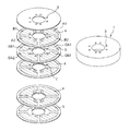
図1は積層電気−機械エネルギー変換素子としての積層圧電素子の分解斜視図および外観斜視図を示しており、本積層圧電素子1は、圧電層になる圧電セラミックスのグリーンシートにスルーホールになる直径0.1mmの穴を開け、その中に導電ペーストを充填しさらにグリーンシートの表面に内部電極層になる電極パターンを導電ペーストを印刷して設け、その後これらのグリーンシートを複数枚重ね加圧し積層化し、焼成してから分極処理を行い最終的に機械加工して得た。
【0022】
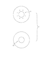
図中、積層圧電素子1は、図13の従来例の積層圧電素子fと同様に、8本のスルーホールによる層間配線2と、素子の一方の端面である表(おもて)面にスルーホールの露出した8個の表面電極3が形成されている。
【0023】
また、内部電極層4は従来例と同じ4分割された内部電極層A1,A2,B1,B2を形成しているが、内部電極層5も4分割された内部電極層GA1,GA2,GB1,GB2を形成している。具体的に積層圧電素子1は、外径10mm、内径2.8mm、厚さ約2.2mm、圧電材層の厚さ85μm、内部電極層の厚さ2〜3μm、内部電極層4と5の外径9.5mm、内部電極層の層数は24層である。振動波駆動装置としての振動波モータの駆動のために、電気的なグランドに相当する内部電極層GA1,GA2,GB1,GB2に対し各々内部電極層A1,A2に振動体の固有振動数にほぼ一致した高周波電圧が、内部電極層B1,B2にA1,A2と90゜の位相差を有する高周波電圧が印加される。
【0024】
また本実施の形態では、図2に示すように、振動波モータを駆動させるために回路基板gを介して電圧が供給される表面電極3のある端面(表面)とは異なるもう一方の端面(裏面)に、電気的なグランドである内部電極層GA1,GA2,GB1,GB2の各層と導通を計る4本のスルーホールが端面(裏面)上に露出し表面電極6が形成されている。この結果、図3に示すように、振動波モータの振動体hに組み込んだ場合には、弾性体である金属ブロックd1 と表面電極6とが接触し導通しており、さらに金属ブロックd1 を介してボルトc、金属ブロックd2 へも導通され、積層圧電素子と同電位となる。
【0025】
なお、本実施の形態では表面電極6は4ヶとしているが、これら4箇の表面電極は全てグランドで同等でもあるので、表面電極6は1ヶでも良い。
【0026】
具体的には内部電極層A1,A2とこれと90゜の位相差を有して内部電極層B1,B2に各々例えば高周波電圧Vp =7Vを印加すると、振動波モータの回転数600rpm、トルク25g・cmの性能が得られ、さらに金属ブロックボルトcも同電位になっているため、性能の安定性も増し前述の欠点であったノイズの問題は解消できた。また、積層圧電素子の製造にも、非常に簡単に表面電極は作れるのでコストの増加もほとんどなく製造可能であった。
【0027】
(第2の実施の形態)
第2の実施の形態は、積層圧電素子の機械的な振動を電気的な信号に変換して出力するため、すなわち、センサとしての制御用の出力を取り出すためのスルーホールの表面電極を設けたものである。
【0028】
振動波モータ駆動時に圧電素子に加わる圧力により発生する電圧を振動波モータの制御に用いることは従来より行なっており、従来例で言えば、図12において、圧電素子a5 が制御用のセンサとして用いられており、その出力は電極板としての金属板b6 を介して取り出すことができる。ただし、詳しくは、電極板b6 と金属ブロックd2 の間には絶縁シートを挟み絶縁を計ったり、高価ではあるが導通しないセラミックス製のブロックを使用している。
【0029】
本実施の形態の積層圧電素子1′は、図4に示すように、表面電極3を有する端面(表面)とは異なるもう一方の端面(裏面)側の一層の1/4の面積の部分にセンサ用の電極層7を設けている。センサ用の電極層7は、スルーホール8により図5に示す素子端面(裏面)に露出した表面電極10と導通している。ここで内部電極層の数はセンサ用の電極層を1層追加して合計25層であり、第1の実施の形態の積層圧電素子に電極層を1層追加した層数である。
【0030】
図6は本実施の形態の積層圧電素子1′を振動波モータの振動体に組み込んだ状態を示す。回路基板g′を使い表面電極10から振動波モータの機械的振動により内部電極層7に発生する電気的信号を外部の回路に取り出すことができる。
この際、センサ用の電極層である内部電極層7の対向する電極層(GA2)は積層圧電素子のグランドと同一であるから、外部回路において信号として電気的に処理されるときには積層圧電素子のグランドを使う。
【0031】
以上の結果、センサ用の電極層を、製造コストをほとんど上げることなく、簡単に追加することが可能で、また駆動用表面電極とは位置的にも離れているので電気的なノイズの影響を受けにくいメリットもあり、振動波モータの周波数制御も容易に可能となった。
【0032】
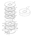
さらに上記した第1の実施の形態と第2の実施の形態とを併用した実施の形態を図7に示す。
【0033】
図7において、センサ用の電極層7の対向するグランド層GA2をスルーホール9により導通させており、このスルーホール9は、図8に示す表面電極11に導通させ、表面電極11は図6の回路基板g′に例えば導通の可能なスルーホールの穴をあけておき、直接金属ブロックd1と接着させ、一方、スルーホール8に繋がる表面電極10は同様に回路基板g′を使い外部回路と導通させることも可能である。
【0034】
以上の例はスルーホールを積層圧電素子の両端面である表面・裏面に露出させ表面電極としたが、露出した表面電極の周囲の表面に電極膜を設けより広い面積をもった電極としても良い。
【0035】
また、図5、図7ではセンサ用の電極層は内部電極層GA2に対向する1/4の面積の部分としたが、内部電極層GA1,GA2またはGB1,GB2に対向して一層の1/2の面積の部分に設けても良い。
【0036】
図9は図7の実施の形態の変形例を示し、この実施の形態の積層圧電素子1′−2が図7の積層圧電素子と異なるのは、電極層7´にスルーホール9” が形成され、該電極層7´を有するグランド層5の直ぐ上の圧電材層には、スルーホール9”に対応してスルーホールが形成されていない点にある。
【0037】
すなわち、センサ用の電極層7と対向するセンサ用のグランドである電極層7′を駆動用のグランド層5の電極層GA1、GB1、GB2とは独立(絶縁)させており、スルーホール9´を用いて図10に示す表面電極11′と導通させることで、表面電極10と11′間でセンサ用の信号電圧を取り出すことができる。
こうすることでセンサ信号は駆動用の電圧からの影響を受けることなく、純粋なセンサ信号のみを取り出すことが可能となる。
【0038】
以上の例では、裏面側のスローホールはグランド用やセンサ用であるが、
単に、駆動用の電圧を供給する際にも、表面ともう一方の面の両面を使ってスルーホールに繋がる表面電極を形成しても良い。将来、とくに小型の振動波モータにおいて、積層圧電素子も小径化しスルーホールを全て片面に設け基板との間で導通を図る際に配線パターンの面積が不足することも考えられ、このような時にも本発明は有効である。
【0039】
【発明の効果】
以上説明したように、本発明によれば非常に簡単に積層圧電素子等の積層電気−機械エネルギー変換素子のグランドを弾性体に電気的に落したり、センサの出力を取り出したりすることが可能であり、製造上もコストアップもほとんどないなどの利点も有する。
【0040】
特にセンサの出力端子として使う表面電極の場合は駆動電圧のノイズの影響が少なく、また必要に応じ従来の積層圧電素子の端面に追加するようなことが可能で振動波モータ等の振動波駆動装置用の積層圧電素子の設計も容易になった。
【0041】
将来、とくに小型の振動波モータにおいて、積層圧電素子も小径化しスルーホールを全て片面に設けると、基板との間で導通を図る配線パターンの面積が不足することも考えられ、このような小型の振動波モータで駆動用の電圧を供給する際にも、表面ともう一方の面の両面を使ってスルーホールに繋がる表面電極を形成した本発明の積層圧電素子は有効である。
【図面の簡単な説明】
【図1】本発明の第1の実施の形態における積層圧電素子の分解斜視図と外観斜視図
【図2】図1の積層圧電素子の両端面に露出した表面電極を示す図
【図3】図1の積層圧電素子を組み込んだ振動波モータの断面図
【図4】本発明の第2の実施の形態における積層圧電素子の分解斜視図と外観斜視図
【図5】図4の積層圧電素子の両端面に露出した表面電極を示す図
【図6】図4の積層圧電素子を組み込んだ振動波モータの断面図
【図7】本発明の第3の実施の形態における積層圧電素子の分解斜視図と外観斜視図
【図8】図7の積層圧電素子の両端面に露出した表面電極を示す図
【図9】本発明の第4の実施の形態における積層圧電素子の分解斜視図と外観斜視図
【図10】図9の積層圧電素子の両端面に露出した表面電極を示す図
【図11】(i)〜(iii)は従来の単板の圧電素子を示す図
【図12】図11の圧電素子を組み込んだ振動波モータの断面図
【図13】従来の積層圧電素子の分解斜視図と外観斜視図
【図14】図13の積層圧電素子の表面と裏面を示す図
【図15】図14の積層圧電素子を組み込んだ振動波モータの断面図
【符号の説明】
1,1′,1″ 本発明の積層圧電素子
3 表面電極
6,10,11 もう一方の端面の表面電極
c ボルト
d1、d2 ブロック
g 回路基板
h 振動体[0001]
BACKGROUND OF THE INVENTION
The present invention relates to a laminated electro-mechanical energy conversion element and a vibration wave driving device formed by alternately laminating a plurality of layers of a material layer having an electro-mechanical energy conversion function and an electrode material layer. The surface electrode connected to the through hole of the element is suitable for a vibration wave driving device such as a vibration wave motor.
[0002]
[Prior art]
As an example of an element as a vibration source of a vibration body constituting a vibration wave driving device such as a vibration wave motor, the element is sandwiched between blocks made of cylindrical metal or ceramic and bent into the block as follows. An element as a vibration generation source of a vibrating body of a rod-shaped vibration wave motor that causes vibration and rotationally moves a contact member in contact with the block by a circular or elliptical movement at any one point on the block surface caused by the bending vibration; There is an element as a vibration generation source of a ring-shaped vibrating body that fixes the element on one surface of a ring-shaped elastic body with, for example, an adhesive and applies a rotational motion by combining two standing waves.
[0003]
Further, as an example of an element used for a rod-like vibration wave motor, the piezoelectric elements described in Japanese Patent Laid-Open Nos. 3-40767 and 3-117384 are shown in FIG. A single plate-like single-plate piezoelectric element a shown in FIG. 2 is a circular region whose front surface coincides with regions (+) and (-) whose polarization directions are opposite in the left and right directions. The electrode material layers (hereinafter referred to as electrode layers) l 1 and l 2 are provided on the piezoelectric material a ′ through the slits S, and the entire back surface is provided with the electrode layer l 3 . Using a plurality of single-plate piezoelectric elements a, a plurality of and 90-degree phase differences are given to some of the piezoelectric elements as in the vibrating body e of a rod-shaped vibration wave motor shown in FIG. Piezoelectric elements a 1 to a 5 are laminated with metal electrode plates b 1 to b 6 connected to an external electric circuit, and assembled with blocks d 1 and d 2 made of metal or ceramics and bolts c. It is fixed.
[0004]
The piezoelectric elements a 1 to a 4 are used for driving, and the piezoelectric element a 5 is used as a sensor for outputting a control signal. In this piezoelectric element a, a piezoelectric material (piezoelectric ceramics), which is generally formed by firing a ceramic powder having piezoelectricity by pressing or extruding, is processed to a constant thickness, processed into a circular shape, and then deposited or printed. The electrode layers l 1 to l 3 are formed by the method, and polarization treatment is performed using these electrode layers to give polarization directions (+) and (−).
[0005]
On the other hand, recently, laminated piezoelectric elements as laminated electro-mechanical energy conversion elements made by alternately laminating piezoelectric material layers and electrode material layers have attracted attention, and attempts have been made to reduce the size and voltage of vibration sources. For example, it is described in JP-A-8-213664. FIG. 13 shows a laminated piezoelectric element f developed for a rod-shaped vibration wave motor. Electrode material layers (hereinafter referred to as internal electrode layers) 4 and 5 are made of a piezoelectric material that has an electromechanical energy conversion function. It is an element that is provided on a layer, stacked alternately, and connected by eight
[0006]
The
[0007]
FIG. 15 shows a cross-sectional view of a vibration wave motor incorporating a laminated piezoelectric element f. The laminated piezoelectric element f is sandwiched between blocks d 1 and d 2 made of an elastic body of metal or ceramics, and at the same time using a wiring board g. The vibrating body h is made by measuring the continuity between each
[0008]
[Problems to be solved by the invention]
In the above two conventional examples, the difference between FIG. 12 which is an example of a vibration wave motor using a plurality of single-plate piezoelectric elements and FIG. 15 which is an example of a vibration wave motor using one laminated piezoelectric element is 2 There is one.
[0009]
One is that the metal blocks d 1 and d 2 and the bolt c are electrically connected to the electrical ground of the piezoelectric element through the metal plates b 1 to b 6 and have the same potential in the example of FIG. No. 15 was not electrically connected to the laminated piezoelectric element, and the metal blocks d 1 and d 2 and the bolt c were in an electrically floating state, that is, in an insulated state. For this reason, in the case of the vibration wave motor using the laminated piezoelectric element shown in FIG. 15, electrical noise is generated due to the generation of floating capacitance or the like.
[0010]
In the example of FIG. 12, one piezoelectric element a 5 is used as a sensor for outputting a control signal, but in the case of FIG. 15, no sensor is provided and the sensor is not used. Since the vibration wave motor was controlled, the fine control performed while sensing the mechanical vibration state of the vibrating body could not be performed.
[0011]
Accordingly, an object of the present invention is to provide a laminated block which can be easily connected between the metal block and the ground of the laminated electro-mechanical energy conversion element and can be used as a sensor using the internal electrode layer of the laminated electro-mechanical energy conversion element. The present invention provides a mechanical energy conversion element and a vibration wave driving device using the electro-mechanical energy conversion element as a vibration source.
[0015]
[Means for Solving the Problems]
In the first invention, the laminated electro-mechanical energy conversion element is disposed between the first elastic body and the second elastic body, and the first elastic body and the second elastic body are fastened by fastening means. Accordingly, in the vibration wave driving apparatus including a vibrating body in which the laminated electro-mechanical energy conversion element is fixed between the first elastic body and the second elastic body, the laminated electro-mechanical energy conversion element A first circuit board provided between one end face of the first electrode and the first elastic body, and provided between the other end face of the laminated electro-mechanical energy conversion element and the second elastic body. The laminated electro-mechanical energy conversion element is formed by alternately laminating a plurality of layers of materials having an electro-mechanical energy conversion function and layers of electrode materials. Between the plurality of electrode material layers A plurality of through holes that tomb conduction, conduction with the plurality of through-holes and the first circuit board, a plurality of first electrodes formed on the surface opposite to the first circuit board, wherein A plurality of second electrodes formed on a surface facing the second circuit board , wherein the plurality of second electrodes are an electrode used as a ground, and the inside of the laminated electro-mechanical energy conversion element An electrode layer that is electrically connected to an electrode layer that generates electrical signals obtained by converting mechanical energy into electrical energy, and the electrode used as the ground is an electrode layer that generates the electrical signals The electrode layer that is electrically connected to the electrode layer that is electrically connected to the electrode layer that generates the electrical signal is insulated from the electrode layer that is electrically connected to the electrode used as the ground of the first electrode. and are And wherein the door.
[0018]
A second invention is the first aspect, wherein the plurality of first electrodes, and wherein the conductive Goku含 Mukoto for high-frequency voltage is applied.
[0020]
DETAILED DESCRIPTION OF THE INVENTION
(First embodiment)
FIG. 1 shows a first embodiment of the present invention.
[0021]
FIG. 1 shows an exploded perspective view and an external perspective view of a laminated piezoelectric element as a laminated electro-mechanical energy conversion element. The laminated
[0022]
In the figure, the laminated
[0023]
Further, the internal electrode layer 4 forms the same four-divided internal electrode layers A1, A2, B1, and B2 as in the conventional example, but the
[0024]
Further, in the present embodiment, as shown in FIG. 2, the other end surface (surface) different from the end surface (surface) having the
[0025]
In the present embodiment, the number of the surface electrodes 6 is four. However, since these four surface electrodes are all equivalent at the ground, the number of the surface electrodes 6 may be one.
[0026]
Specifically, when a high frequency voltage Vp = 7 V, for example, is applied to the internal electrode layers A1 and A2 and the internal electrode layers B1 and B2 with a phase difference of 90 ° from the internal electrode layers A1 and A2, the rotational speed of the vibration wave motor is 600 rpm and torque is 25 g. Since the performance of cm was obtained and the metal block bolt c was also at the same potential, the stability of the performance was increased and the noise problem which was the above-mentioned drawback could be solved. In addition, since the surface electrode can be made very easily in the production of the laminated piezoelectric element, it can be produced with almost no increase in cost.
[0027]
(Second Embodiment)
In the second embodiment, a surface electrode of a through hole is provided for converting the mechanical vibration of the laminated piezoelectric element into an electrical signal and outputting it, that is, for taking out a control output as a sensor. Is.
[0028]
Conventionally, the voltage generated by the pressure applied to the piezoelectric element when the vibration wave motor is driven is used for controlling the vibration wave motor. In the conventional example, in FIG. 12, the piezoelectric element a 5 is used as a control sensor. The output can be taken out through a metal plate b 6 as an electrode plate. However, in detail, an insulating sheet is sandwiched between the electrode plate b 6 and the metal block d 2 to measure insulation, or an expensive but non-conductive ceramic block is used.
[0029]
As shown in FIG. 4, the multilayer
[0030]
FIG. 6 shows a state in which the laminated
At this time, since the opposing electrode layer (GA2) of the
[0031]
As a result of the above, it is possible to easily add an electrode layer for a sensor with almost no increase in manufacturing cost, and since it is distant from the surface electrode for driving, the influence of electrical noise is reduced. There is also a merit that it is difficult to receive, and the frequency control of the vibration wave motor can be easily performed.
[0032]
Further, FIG. 7 shows an embodiment in which the first embodiment and the second embodiment described above are used in combination.
[0033]
In FIG. 7, the ground layer GA2 opposite to the
[0034]
In the above example, through holes are exposed on the front and back surfaces, which are both end faces of the laminated piezoelectric element, to form surface electrodes. However, an electrode film may be provided on the surface around the exposed surface electrode to form an electrode having a larger area. .
[0035]
In FIGS. 5 and 7, the sensor electrode layer is a portion having an area of 1/4 facing the internal electrode layer GA2. However, the sensor electrode layer is 1/1 layer facing the internal electrode layers GA1, GA2 or GB1, GB2. You may provide in the part of 2 area.
[0036]
FIG. 9 shows a modification of the embodiment of FIG. 7. The laminated
[0037]
That is, the
By doing so, the sensor signal is not affected by the driving voltage, and only a pure sensor signal can be extracted.
[0038]
In the above example, the slow hole on the back side is for ground or sensor,
When supplying a driving voltage, a surface electrode connected to the through hole may be formed using both the surface and the other surface. In the future, especially in small-sized vibration wave motors, it is considered that the laminated piezoelectric element is also reduced in diameter, and when the through-holes are all provided on one side and conduction with the substrate is attempted, the area of the wiring pattern will be insufficient. The present invention is effective.
[0039]
【Effect of the invention】
As described above, according to the present invention, it is possible to electrically drop the ground of a laminated electromechanical energy conversion element such as a laminated piezoelectric element to an elastic body or take out the output of the sensor. There is also an advantage that there is almost no increase in manufacturing and cost.
[0040]
In particular, in the case of a surface electrode used as an output terminal of a sensor, the influence of the noise of the driving voltage is small, and it can be added to the end face of a conventional multilayer piezoelectric element if necessary, and a vibration wave driving device such as a vibration wave motor The design of laminated piezoelectric elements for use has also become easier.
[0041]
In the future, especially in a small vibration wave motor, if the laminated piezoelectric element is also reduced in diameter and all the through holes are provided on one side, it is possible that the area of the wiring pattern that conducts with the substrate will be insufficient. Even when a driving voltage is supplied by a vibration wave motor, the multilayer piezoelectric element of the present invention in which the surface electrode connected to the through hole is formed using both the surface and the other surface is effective.
[Brief description of the drawings]
FIG. 1 is an exploded perspective view and an external perspective view of a multilayer piezoelectric element according to a first embodiment of the present invention. FIG. 2 is a diagram showing surface electrodes exposed on both end faces of the multilayer piezoelectric element of FIG. FIG. 4 is a cross-sectional view of a vibration wave motor incorporating the multilayer piezoelectric element of FIG. 1. FIG. 4 is an exploded perspective view and an external perspective view of the multilayer piezoelectric element in the second embodiment of the present invention. FIG. 6 is a cross-sectional view of a vibration wave motor incorporating the laminated piezoelectric element of FIG. 4; FIG. 7 is an exploded perspective view of the laminated piezoelectric element according to the third embodiment of the present invention. FIG. 8 is a perspective view of the multilayer piezoelectric element shown in FIG. 7. FIG. 9 is an exploded perspective view of the multilayer piezoelectric element according to the fourth embodiment of the present invention. FIG. 10 is a diagram showing surface electrodes exposed on both end faces of the multilayer piezoelectric element of FIG. FIG. 12 is a sectional view of a vibration wave motor incorporating the piezoelectric element of FIG. 11. FIG. 13 is an exploded perspective view of a conventional multilayer piezoelectric element. FIG. 14 is a perspective view of the multilayer piezoelectric element of FIG. 13. FIG. 15 is a sectional view of a vibration wave motor incorporating the multilayer piezoelectric element of FIG.
1,1 ′, 1 ″ Multilayer
Claims (2)
前記積層電気−機械エネルギー変換素子の一方の端面と前記第1の弾性体との間に設けられた第1の回路基板と、
前記積層電気−機械エネルギー変換素子の他方の端面と前記第2の弾性体との間に設けられた第2の回路基板と、を有し、
前記積層電気−機械エネルギー変換素子は、電気−機械エネルギー変換機能を有する材料の層と電極材料の層が交互に複数重ねて積層化されたものであって、
前記複数の電極材料の層の間の導通をはかる複数のスルーホールと、
前記複数のスルーホール及び前記第1の回路基板と導通し、前記第1の回路基板に対向する面に形成された複数の第1の電極と、
前記第2の回路基板に対向する面に形成された複数の第2の電極と、を有し
前記複数の第2の電極は、グランドとして用いられる電極と、前記積層電気−機械エネルギー変換素子内部に設けられ機械エネルギーを電気エネルギーに変換して得られる電気的な信号を発生する電極層と導通する電極と、を含み、
前記グランドとして用いられる電極は、前記電気的な信号を発生する電極層と対向する電極層と導通しており、
前記電気的な信号を発生する電極層と対向する電極層は、前記第1の電極のうちグランドとして用いられる電極と導通する電極層とは、絶縁されていることを特徴とする振動波駆動装置。A laminated electro-mechanical energy conversion element is disposed between the first elastic body and the second elastic body, and the first elastic body and the second elastic body are fastened by a fastening means, whereby the first In a vibration wave driving device including a vibrating body in which the laminated electro-mechanical energy conversion element is fixed between one elastic body and the second elastic body,
A first circuit board provided between one end face of the laminated electro-mechanical energy conversion element and the first elastic body;
A second circuit board provided between the other end face of the laminated electro-mechanical energy conversion element and the second elastic body,
The laminated electro-mechanical energy conversion element is formed by alternately laminating a plurality of layers of materials having an electro-mechanical energy conversion function and layers of electrode materials,
A plurality of through holes for conducting between the layers of the plurality of electrode materials;
A plurality of first electrodes formed on a surface that is electrically connected to the plurality of through-holes and the first circuit board and faces the first circuit board ;
Anda plurality of second electrodes formed on the surface facing the second circuit board
The plurality of second electrodes are electrically connected to an electrode that is used as a ground and an electrode layer that is provided inside the laminated electro-mechanical energy conversion element and generates an electrical signal obtained by converting mechanical energy into electrical energy. An electrode to be
The electrode used as the ground is electrically connected to the electrode layer facing the electrode layer that generates the electrical signal,
The vibration wave driving device characterized in that the electrode layer facing the electrode layer that generates the electrical signal is insulated from the electrode layer that is electrically connected to the electrode used as the ground in the first electrode. .
Priority Applications (1)
| Application Number | Priority Date | Filing Date | Title |
|---|---|---|---|
| JP2001232254A JP5031153B2 (en) | 2001-07-31 | 2001-07-31 | Laminated electro-mechanical energy conversion element and vibration wave drive device |
Applications Claiming Priority (1)
| Application Number | Priority Date | Filing Date | Title |
|---|---|---|---|
| JP2001232254A JP5031153B2 (en) | 2001-07-31 | 2001-07-31 | Laminated electro-mechanical energy conversion element and vibration wave drive device |
Publications (3)
| Publication Number | Publication Date |
|---|---|
| JP2003046156A JP2003046156A (en) | 2003-02-14 |
| JP2003046156A5 JP2003046156A5 (en) | 2008-09-18 |
| JP5031153B2 true JP5031153B2 (en) | 2012-09-19 |
Family
ID=19064200
Family Applications (1)
| Application Number | Title | Priority Date | Filing Date |
|---|---|---|---|
| JP2001232254A Expired - Fee Related JP5031153B2 (en) | 2001-07-31 | 2001-07-31 | Laminated electro-mechanical energy conversion element and vibration wave drive device |
Country Status (1)
| Country | Link |
|---|---|
| JP (1) | JP5031153B2 (en) |
Families Citing this family (4)
| Publication number | Priority date | Publication date | Assignee | Title |
|---|---|---|---|---|
| JP4576185B2 (en) * | 2004-09-22 | 2010-11-04 | オリンパス株式会社 | Ultrasonic transducer |
| JP4829495B2 (en) * | 2004-12-21 | 2011-12-07 | キヤノン株式会社 | Vibration wave drive |
| JP2006186099A (en) * | 2004-12-27 | 2006-07-13 | Canon Inc | Laminated piezoelectric element and oscillatory wave driving device |
| JP5074674B2 (en) * | 2005-07-04 | 2012-11-14 | キヤノン株式会社 | Multilayer piezoelectric element and vibration wave motor |
Family Cites Families (5)
| Publication number | Priority date | Publication date | Assignee | Title |
|---|---|---|---|---|
| JP3170634B2 (en) * | 1993-12-01 | 2001-05-28 | キヤノン株式会社 | Ultrasonic transducer and ultrasonic drive |
| JP3402816B2 (en) * | 1994-12-22 | 2003-05-06 | キヤノン株式会社 | Ultrasonic motor drive circuit |
| JP3432321B2 (en) * | 1995-01-31 | 2003-08-04 | 太平洋セメント株式会社 | Multilayer ceramic piezoelectric element |
| JP3867823B2 (en) * | 1998-03-13 | 2007-01-17 | キヤノン株式会社 | Manufacturing method of laminated piezoelectric element |
| JPH11252956A (en) * | 1998-03-02 | 1999-09-17 | Star Micronics Co Ltd | Laminated piezoelectric element and ultrasonic motor using the same |
-
2001
- 2001-07-31 JP JP2001232254A patent/JP5031153B2/en not_active Expired - Fee Related
Also Published As
| Publication number | Publication date |
|---|---|
| JP2003046156A (en) | 2003-02-14 |
Similar Documents
| Publication | Publication Date | Title |
|---|---|---|
| US7592738B2 (en) | Ultrasonic motor | |
| CN1538612B (en) | Ultrasonic vibrator and ultrosonic electric machine | |
| JP3311446B2 (en) | Ultrasonic motor | |
| JP5665522B2 (en) | Vibrating body and vibration type driving device | |
| US6114798A (en) | Stacked element and vibration drive device | |
| US9135906B2 (en) | Ultrasonic generator | |
| JP5298999B2 (en) | Multilayer piezoelectric element | |
| JP2001352768A (en) | Multilayer electromechanical energy conversion element and oscillation wave driver | |
| US5448127A (en) | Vibration wave driven motor | |
| JP5031153B2 (en) | Laminated electro-mechanical energy conversion element and vibration wave drive device | |
| JP2003009555A (en) | Laminated electrical energy-mechanical energy transducer and vibration wave drive device | |
| JP3416233B2 (en) | Laminated piezoelectric element, polarization processing method for laminated piezoelectric element, ultrasonic motor, and apparatus equipped with ultrasonic motor | |
| JP4666578B2 (en) | Ultrasonic vibration element and ultrasonic actuator using the same | |
| JP3311034B2 (en) | Laminated piezoelectric element, method for manufacturing laminated piezoelectric element, vibration wave driving device, and apparatus equipped with vibration wave driving device | |
| JPH08308268A (en) | Laminated type piezoelectric element and its polarization treatment method, oscillatory wave motor, and driver | |
| JP3313782B2 (en) | Multilayer piezoelectric element, method of manufacturing the same, method of polarization, vibration wave driving device, and equipment equipped with vibration wave driving device | |
| JP2003046156A5 (en) | ||
| JP2006320119A (en) | Ultrasonic motor | |
| JPH11307835A (en) | Manufacture of sheared piezoelectric element of laminating structure | |
| KR20130087478A (en) | Ultrasound probe | |
| JP2019216203A (en) | Piezoelectric element, vibration waveform sensor, and vibration waveform sensor module | |
| WO2020179731A1 (en) | Vibration sensor | |
| JP2011155126A (en) | Piezoelectric laminated component | |
| JP2005223968A (en) | Oscillator and oscillatory wave driver | |
| JPH0628951Y2 (en) | Piezoelectric actuator |
Legal Events
| Date | Code | Title | Description |
|---|---|---|---|
| A521 | Request for written amendment filed |
Free format text: JAPANESE INTERMEDIATE CODE: A523 Effective date: 20080731 |
|
| A621 | Written request for application examination |
Free format text: JAPANESE INTERMEDIATE CODE: A621 Effective date: 20080731 |
|
| RD01 | Notification of change of attorney |
Free format text: JAPANESE INTERMEDIATE CODE: A7421 Effective date: 20081031 |
|
| RD04 | Notification of resignation of power of attorney |
Free format text: JAPANESE INTERMEDIATE CODE: A7424 Effective date: 20100201 |
|
| RD01 | Notification of change of attorney |
Free format text: JAPANESE INTERMEDIATE CODE: A7421 Effective date: 20100630 |
|
| A977 | Report on retrieval |
Free format text: JAPANESE INTERMEDIATE CODE: A971007 Effective date: 20120105 |
|
| A131 | Notification of reasons for refusal |
Free format text: JAPANESE INTERMEDIATE CODE: A131 Effective date: 20120117 |
|
| A521 | Request for written amendment filed |
Free format text: JAPANESE INTERMEDIATE CODE: A523 Effective date: 20120314 |
|
| A131 | Notification of reasons for refusal |
Free format text: JAPANESE INTERMEDIATE CODE: A131 Effective date: 20120403 |
|
| A521 | Request for written amendment filed |
Free format text: JAPANESE INTERMEDIATE CODE: A523 Effective date: 20120604 |
|
| TRDD | Decision of grant or rejection written | ||
| A01 | Written decision to grant a patent or to grant a registration (utility model) |
Free format text: JAPANESE INTERMEDIATE CODE: A01 Effective date: 20120626 |
|
| A01 | Written decision to grant a patent or to grant a registration (utility model) |
Free format text: JAPANESE INTERMEDIATE CODE: A01 |
|
| A61 | First payment of annual fees (during grant procedure) |
Free format text: JAPANESE INTERMEDIATE CODE: A61 Effective date: 20120627 |
|
| FPAY | Renewal fee payment (event date is renewal date of database) |
Free format text: PAYMENT UNTIL: 20150706 Year of fee payment: 3 |
|
| LAPS | Cancellation because of no payment of annual fees |